

Samsung SGH-J600 Service Manual
Specification
1.
GSM/DCS1800/PCS1900 General Specification
1-1.
EGSM 900
Phase 2
Freq. Band[MHz]
Uplink/Downlink
ARFCN range 0~124 & 975~1023 512~885 512~810
Tx/Rx spacing 45
Mod. Bit rate/
Bit Period
Time Slot
Period/Frame
Period
Modulation 0.3
880~915
925~960
270.833
3.692
576.9
4.615
GMSK
MHz
kbps
us
us
ms
DCS1800
Phase 1
1710~1785
1805~1880
MHz
95
270.833
3.692
576.9
4.615
GMSK
0.3
kbps
us
us
ms
PCS1900
1850~1910
1930~1990
80
270.833
3.692
576.9
4.615
GMSK
0.3
MHz
kbps
us
us
ms
MS Power 33
Power Class 5
Sensitivity -102
TDMA Mux 8 8 8
Cell Radius 35
dBm~5 dBm
pcl
~19
dBm
Km
pcl
dBm~0 dBm
30
pcl
0
~15
-100
2
dBm
Km
pcl
dBm~0 dBm
30
pcl
0
-100
~15
dBm
-
pcl
1-1
SAMSUNG Proprietary-Contents may change without notice
This Document can not be used without Samsung's authorization
Specification
GSM TX power class
1-2.
TX Power
control level
EGSM900
533±2
631±2
729±2
827±2
925±2
10 23±2
11 21±2
dBm
dBm
dBm
dBm
dBm
dBm
dBm
TX Power
DCS1800
control level
030±3
128±3
226±3
324±3
422±3
520±3
618±3
dBm
dBm
dBm
dBm
dBm
dBm
dBm
TX Power
control level
PCS1900
030±3
128±3
226±3
324±3
422±3
520±3
618±3
dBm
dBm
dBm
dBm
dBm
dBm
dBm
12 19±2
13 17±2
14 15±2
15 13±2
16 11±3
17 9± 3
18 7±3
19 5±3
dBm
dBm
dBm
dBm
dBm
dBm
dBm
dBm
716±3
814±3
912±4
10 10±4
11 8±4
12 6±4
13 4±4
14 2±5
dBm
dBm
dBm
dBm
dBm
dBm
dBm
dBm
716±3
814±3
912±4
10 10±4
11 8±4
12 6±4
13 4±4
14 2±5
dBm
dBm
dBm
dBm
dBm
dBm
dBm
dBm
15 0±5
1-2
SAMSUNG Proprietary-Contents may change without notice
This Document can not be used without Samsung's authorization
dBm
15 0±5
dBm
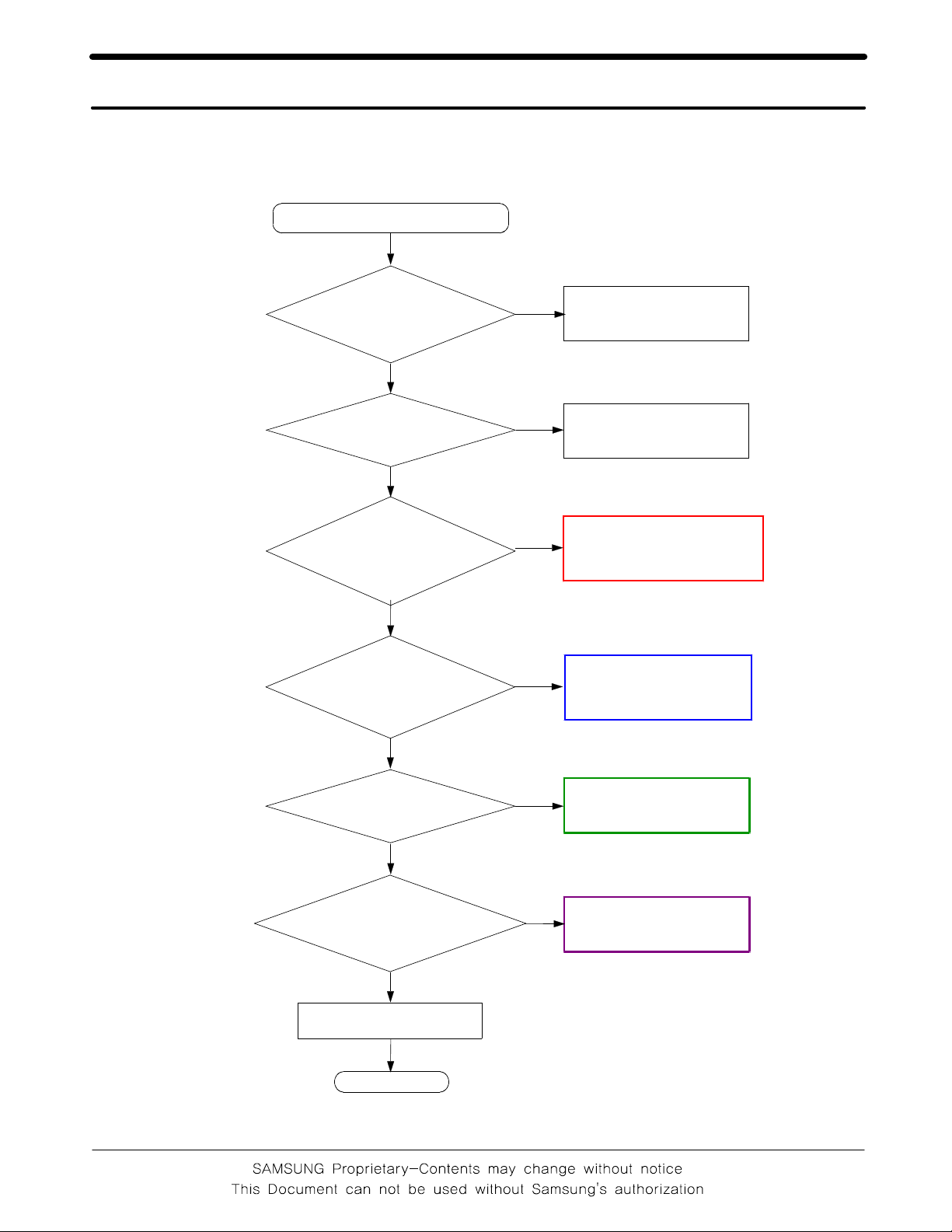
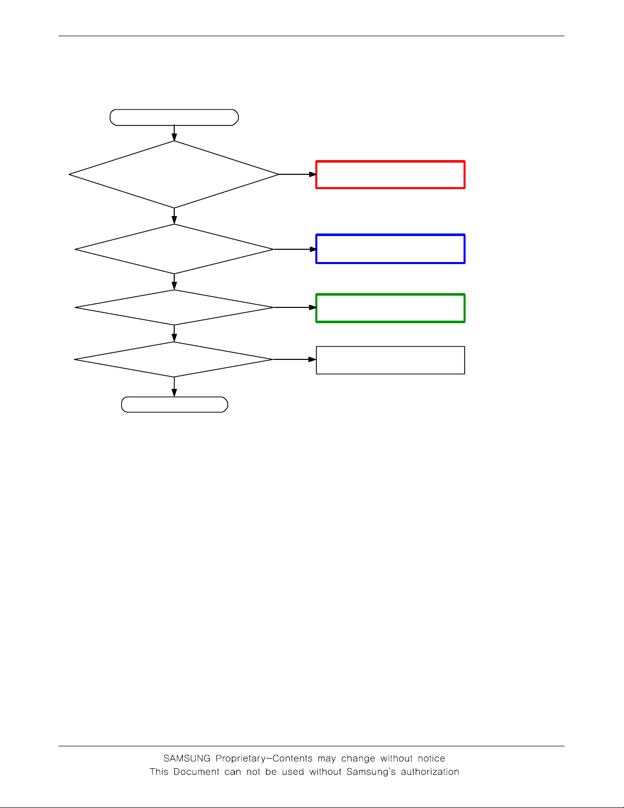
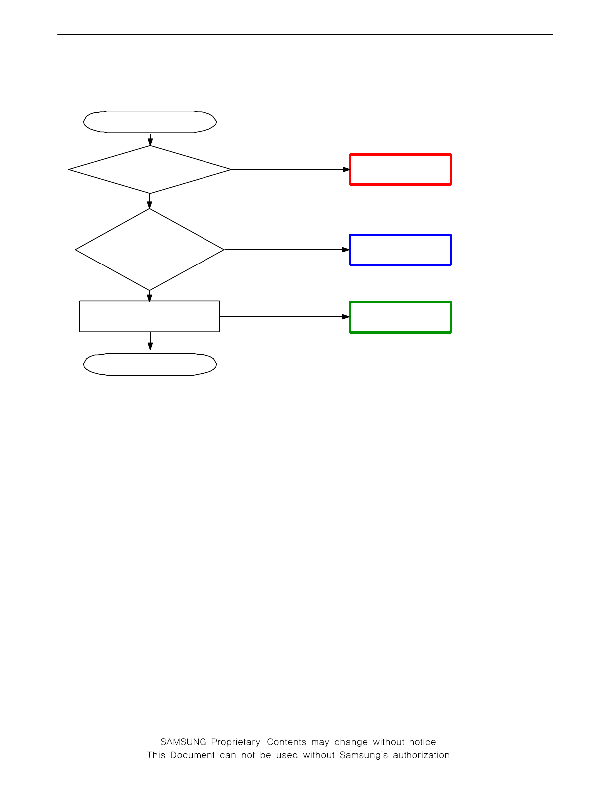
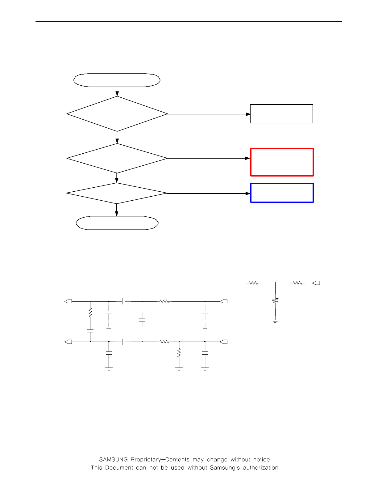
3. Flow Chart of Troubleshooting
BASEBAND
3-1
3-1-1.
Power ON
Power On' does not work
'
Yes
Check the current
consumption more
than
Check the VBAT
more than
CCD_
V
VCCD_1.8V
ofUCD
100
Yes
Yes
Check the
1.2V_C ,
is more
300
than
1.2V
Yes
mA
3.3V
No
No
No
Download again
Charge the Battery
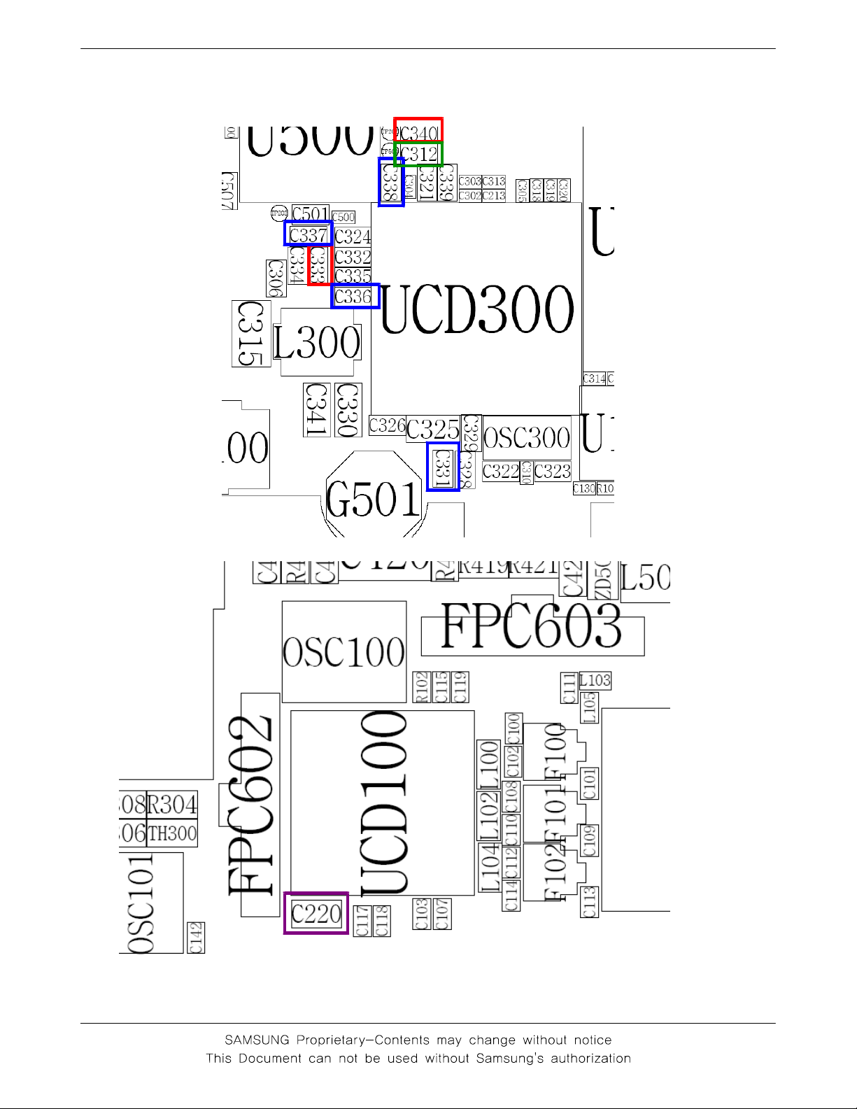
①
CheckUCD
C3
33 ,
300
C340
and
VCCD_1.2V_B/A
VCCD_2.9V
VCCA_2.8V
Check VRF of
UCD300=2.9V
Check C220
Freq
Vp-p
Check the initial operation
Yes
Yes
=26
>0.8V
Yes
Yes
END
=1.2V
=2.9V
=2.8V
MHz
UCD30
Check
No
No
No
②
CheckUCD300 and
C334/C335,C339,C338
③
CheckUCD
and C3
300
12
④
Check the clock C220
3-1
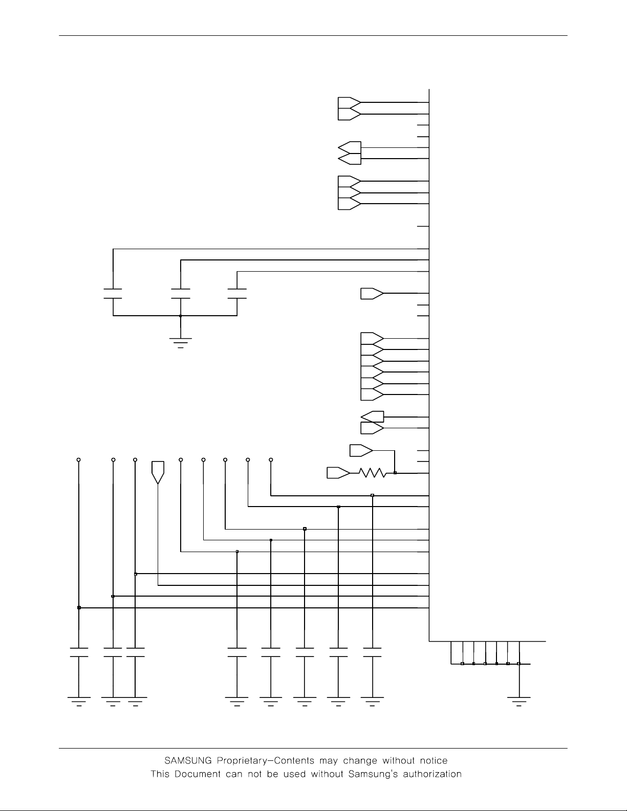
Flow Chart of Troubleshooting
C318
C
_
V
2
.
1
_
D
C
C
V
3
3
3
C
4
3
3
C
C319
B
A
_
_
V
V
2
2
.
.
1
1
_
_
D
D
C
C
C
C
V
V
K15
RADIO_L
RADIO_R
STEREO_OUT_L
STEREO_OUT_R
PWR_KEEP
JIG_ON
PWR_ON
C320
KEY_BACKLIGHT
RXTX_DATA
RXTX_EN
S
_
A
E
R
O
C
_
O
D
L
V
V
V
8
9
.
V
V
8
8
.
.
2
1
_
_
T
D
B
S
V
V
.
2
2
_
_
A
D
C
C
C
C
V
V
RXTX_I_N
RXTX_I_P
RXTX_Q_N
V
RXTX_Q_P
8
.
1
_
D
C
C
V
TXPSTB
VEXT_ABB
VAPC
USB_5V
R309
5
3
3
C
6
3
3
C
7
3
3
C
8
3
3
C
9
3
3
C
0
4
3
C
STEREO1_IN_L
K14
STEREO1_IN_R
H11
STEREO2_IN_L/M
J12
STEREO2_IN_R/M
M14
STEREO_OUT_L
M13
STEREO_OUT_R
P6
PWR_KEEP
E5
PWR_SW2
C4
PWR_SW1N
F14
MIC_B_D
J5
RAREF1
H6
RAREF2
J6
RAREF3
D7
LED1_DRV
C7
LED2_DRV
D9
LED3_DRV
N2
RXTXDATA
R2
RXTXEN
J4
RXTXIN
J3
RXTXIP
K3
RXTXQN
K4
RXTXQP
H5
TXP
L5
TXPSTB
P13
USB_CARKIT_D_N
P12
USB_CARKIT_D_P
C10
USB_CHRG
A6
VLDO_1
D6
VLDO_2
E14
VLDO_AUD
F12
VLDO_AUX1
D14
VLDO_AUX2
C15
VLDO_COREA
B15
VLDO_COREA_S
C12
VLDO_COREB
D13
VLDO_COREC
6
K
D
S
Q
S
S
S
V
V
8
K
N
N
S
V
G
G
1
9
1
1
K
K
N
B
D
D
S
S
S
D
D
D
N
N
N
G
G
G
0
4
6
1
F
F
E
3-2
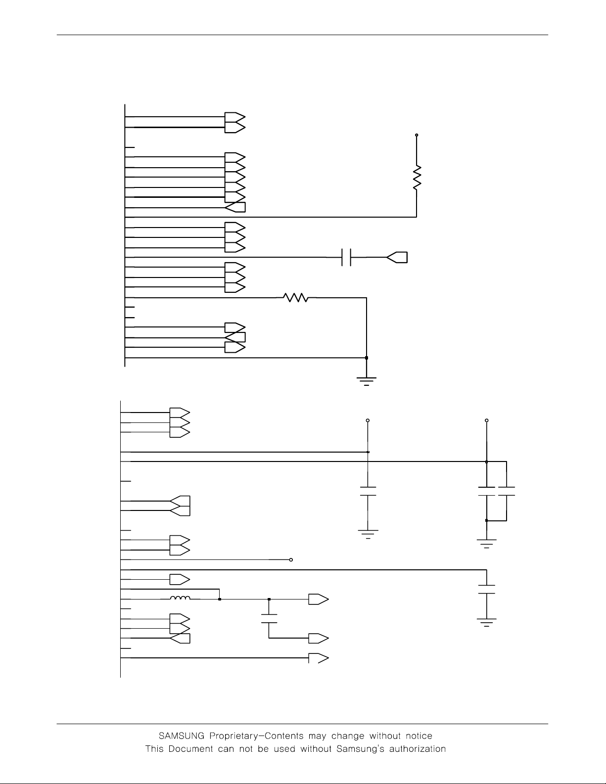
Flow Chart of Troubleshooting
RXTXDAT
RXTXEN
DQ
WEN
OEN
IOBIT_0_RTCK
FLASHRSTN
PWRKEEP
RESETN
RFVDDSEL
SCUSTB
SMADDRVALID
SMCLK
SYSCLK
TCK
TDI
TDO
TEST_0
TEST_1
TEST_2
TMS
TRSTN
TXPSTB
UART0VDDSEL
K15
M18
A14
F5
H1
H16
T2
R12
R15
H18
M17
A1
B4
F17
U13
V13
T14
V14
R10
W17
U12
W14
K18
T16
RXTX_DATA
RXTX_EN
CP_WEN
CP_OEN
RTCK
FLASH_RST
PWR_KEEP
TI_RST
SCUSTB
SM_ADDR_VALID
SM_CLK
TCK
TDI
TDO
R218
TMS
TRSTN
TXPSTB
VCCD_1.8V
R211
CLK26M_DBB
C220
UP_CLK
UP_IO
UP_RST
VRFLDO_1
VRFLDO_2
VREF
CNTL_DAT_CSP
CNTL_EN_CSP
HV_CHRG
AFC
AINT
BATKELV
CREF
DINT
FBSW
LX
NC1
PSW1_BUF
RTC_CLK
SCUSTB
VACC
VEXT
N5
L6
M6
E3
F3
F2
P1
N9
D10
G5
N7
B11
F1
L9
B12
B13
D3
L10
R3
P3
C9
A12
F5
L300
SIMCLK
SIMDATA
SIMRST
CNTL_DAT_CSP
CNTL_EN_CSP
AFC
AINT
DINT
PSW1_BUF
RTC_CLK
SCUSTB
VBAT
C315
VSYN_2.8V
DCDC_OUT
GND_SW
VEXT_ABB
C312
VRF_2.9V
C313C310
C314
3-3
Flow Chart of Troubleshooting
3-4
Flow Chart of Troubleshooting
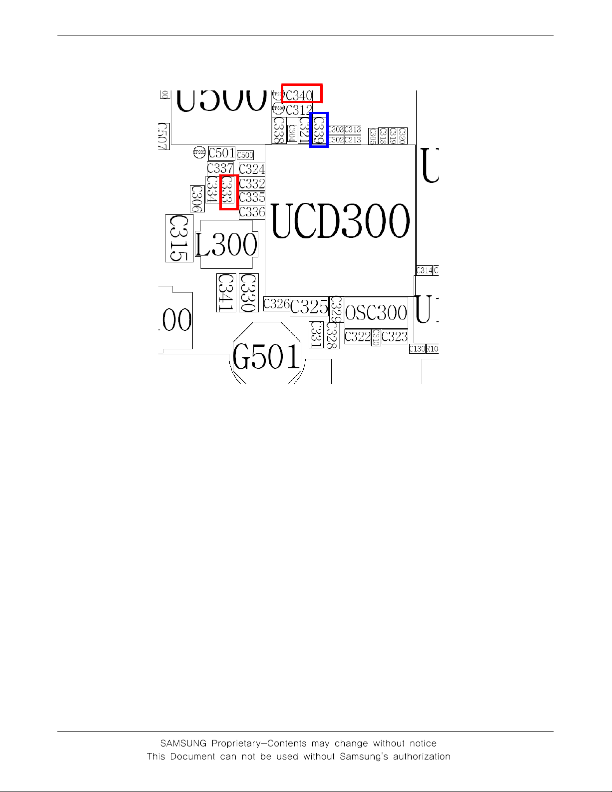
3-1-2.
Initial
Initial Failure
Check VCCD_1.2V_C,
VCCD_1.8V of UCD300
"High" when the phone
is boot on`
Check
the VCCD_2.9V of
UCD300 is "High"
LCD display is O.K?
Sound is O.K?
Yes
Yes
Yes
Yes
Yes
No
No
No
No
①
Chec k UCD300 and
C333 , C340
②
Check UCD300 and C339
③
Check HEA601 and LCD par t
Chec k audi o part
END
3-5
Flow Chart of Troubleshooting
C318
3
3
3
C
C319
A
B
C
_
_
_
V
V
V
2
2
2
.
.
.
1
1
1
_
_
_
D
D
D
C
C
C
C
C
C
V
V
V
4
3
3
C
C320
S
_
A
E
R
V
O
8
C
.
_
1
_
O
T
D
B
L
V
V
5
3
3
C
STEREO_OUT_L
STEREO_OUT_R
V
8
.
V
2
8
.
_
2
A
_
C
D
C
S
V
V
6
3
3
C
RADIO_L
RADIO_R
PWR_KEEP
JIG_ON
PWR_ON
KEY_BACKLIGHT
RXTX_DATA
RXTX_EN
RXTX_I_N
RXTX_I_P
RXTX_Q_N
V
V
RXTX_Q_P
8
9
.
.
1
2
_
_
D
D
C
C
V
C
C
V
VEXT_ABB
TXPSTB
USB_5V
7
8
3
3
3
3
C
C
VAPC
9
3
3
C
R309
K15
STEREO1_IN_L
K14
STEREO1_IN_R
H11
STEREO2_IN_L/M
J12
STEREO2_IN_R/M
M14
STEREO_OUT_L
M13
STEREO_OUT_R
P6
PWR_KEEP
E5
PWR_SW2
C4
PWR_SW1N
F14
MIC_B_D
J5
RAREF1
H6
RAREF2
J6
RAREF3
D7
LED1_DRV
C7
LED2_DRV
D9
LED3_DRV
N2
RXTXDATA
R2
RXTXEN
J4
RXTXIN
J3
RXTXIP
K3
RXTXQN
K4
RXTXQP
H5
TXP
L5
TXPSTB
P13
USB_CARKIT_D_N
P12
USB_CARKIT_D_P
C10
USB_CHRG
A6
VLDO_1
D6
VLDO_2
E14
VLDO_AUD
F12
VLDO_AUX1
D14
VLDO_AUX2
C15
VLDO_COREA
B15
VLDO_COREA_S
C12
VLDO_COREB
D13
0
4
3
C
VLDO_COREC
S
S
V
6
K
Q
S
D
S
B
D
D
D
D
D
S
S
N
N
N
N
N
S
S
V
V
G
G
G
G
G
1
0
9
8
1
6
4
1
1
F
F
K
K
K
E
N
LCD_DO(1)
LCD_DO(3)
LCD_DO(5)
LCD_DO(7)
LCD_RS_O
LCD_WEN_O
LCD_CS_O
PCLK
CAM_Y(7)
CAM_Y(5)
CAM_Y(3)
CAM_SCL
CAM_RST
TOUCH_SDA
TOUCH_EN
KEY_COL(0)
KEY_COL(1)
KEY_COL(2)
KEY_ROW(5)
KEY_ROW(4)
VCCD_2.9V
C600
HEA601
22
11
55
66
77 88
99
10
12
11
11
13 14
13
15 16
15
17 18
17
20
19
19
21 22
21
23 24
23
252526
27 28
27
293330
29
31 32
31
34
33
33
35 36
35
37 38
37
394440
39
41
42
41 42
43
44
43 44
45
46
45 46
47
48
47 48
49
50
49
VBAT
LCD_DO(0)
LCD_DO(2)
LCD_DO(4)
10
12
14
16
18
20
22
24
26
28
30
32
34
36
38
40
LCD_DO(6)
LCD_BL_EN
LCD_REN_O
VSYNC
HSYNC
MCLK
CAM_Y(6)
CAM_Y(4)
CAM_Y(2)
CAM_Y(0)CAM_Y(1)
CAM_SDA
CAMPWR_EN
TOUCH_SCL
TOUCH_IRQ
MOTOR_EN
SPK+
50
SPK-
3-6
Flow Chart of Troubleshooting
3-7
Flow Chart of Troubleshooting
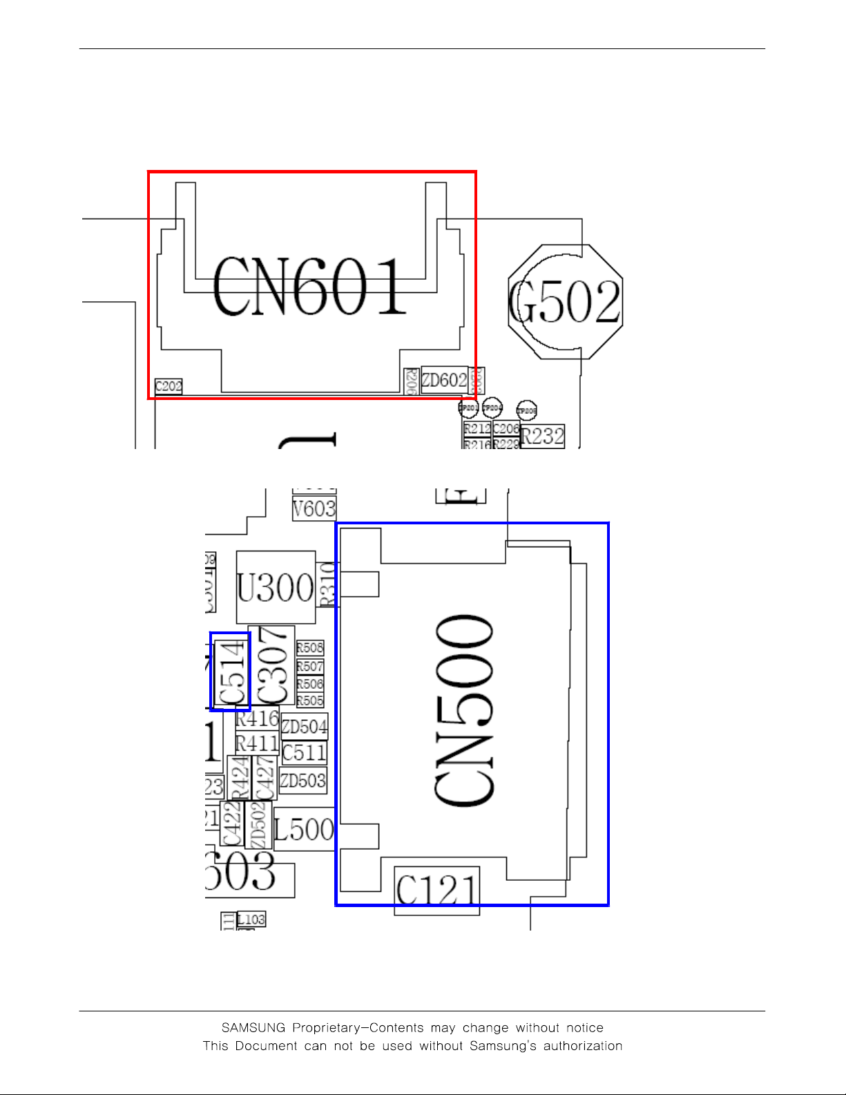
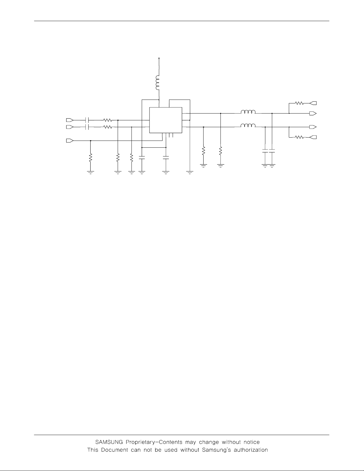
3-1-3.
Sim Part
Phone can't access
SIM card
Check the pin 1 of
CN602( SIM)
Volt ag e = 3V
Check the SIM
connec tor' s
(CN602)
connec tor' s to SIM
card
Check the circuit aroun d CN60 2
input circuitry
END
YES
YES
YES
NO
NO
NO
①
Check the circuit related to
CN602
②
resolder or change
CN602
③
Check the relate d circuit of
CN602
3-8
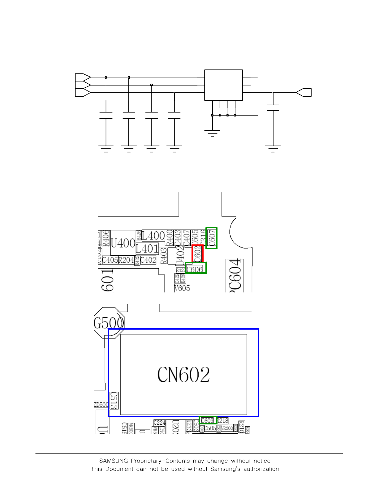
VSIM
SIM_RST
CN602
11
22
3
3
Flow Chart of Troubleshooting
6
6
5
5
4
4
7GG89GG10
SIM_IOSIM_CLK
C603
C605
C606 C607C602
3-9
Flow Chart of Troubleshooting
3-1-4.
Charging Part
Abn or mal charging part
Yes
The pin #19,#20 of
IFC501 = 5V?
Yes
The pin #4 of U300 is
Low?
Yes
The pin #8 of U300 is
3.5 ~ 4.2V?
Yes
The pin #4 of U301 is
HIGH?
Yes
END
No
No
No
No
①
Check TA & IFC 501
②
Chec k th e R313 & U300
Chec k th e U300
Chec k th e U301
3-10
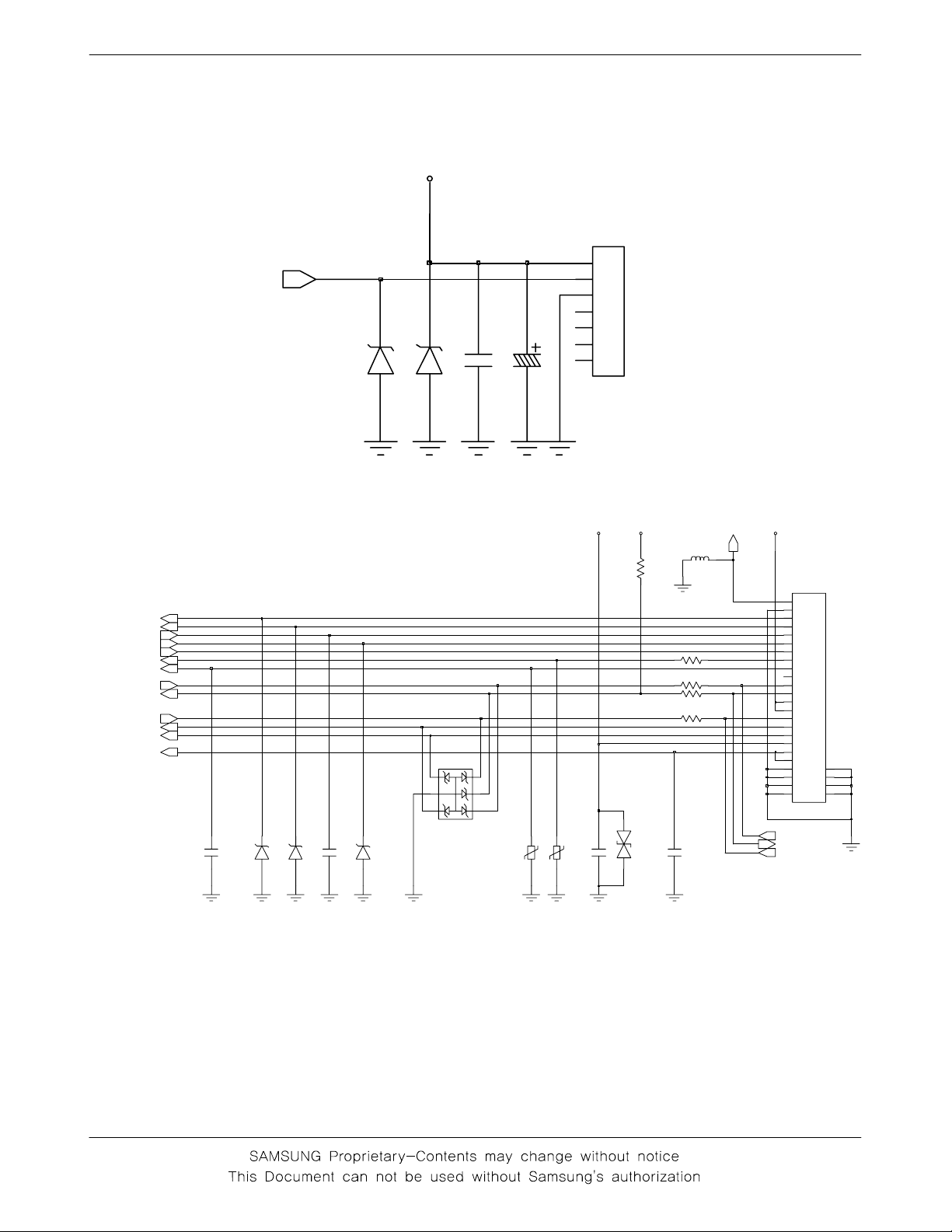
BATT_OPEN_CHECK
Flow Chart of Troubleshooting
VBAT
CN601
1
1
2
2
3
3
4
NC
5
NC
6
NC
7
NC
2
0
6
D
Z
3
0
6
D
Z
EAR_MIC+
EAR_MIC-
EAR_R
EAR_COMN
EAR_L
EAR_SWITCH
EAR_JACK_IN
SDS_TXD
SDS_RXD
JIG_ON
USB_D+
USB_D-
VEXT_5V
C515
ZD502
ZD503
C511
NC
ZD504
C604
U501
6
1
5
2
34
C601
0
0
5
R
V
USB_5V
R504
ZD500
1
C513
0
5
R
V
C514
R505
R506
R507
R508
RADIO_ANT
L500
VBATVCCD_1.8V
10
11
12
13
14
15
16
17
18
19
20
21
22
23
24
SDS_TXD_J
SDS_RXD_J
JIG_ON_J
CN500
1
1
2
2
3
3
4
4
5
5
6
6
7
7
8
8
9
9
10
11
12
13
14
15
16
17
18
19
20
NC
NC
NC
NC
25
NC
26
NC
27
NC
28
NC
3-11
Flow Chart of Troubleshooting
3-12
Flow Chart of Troubleshooting
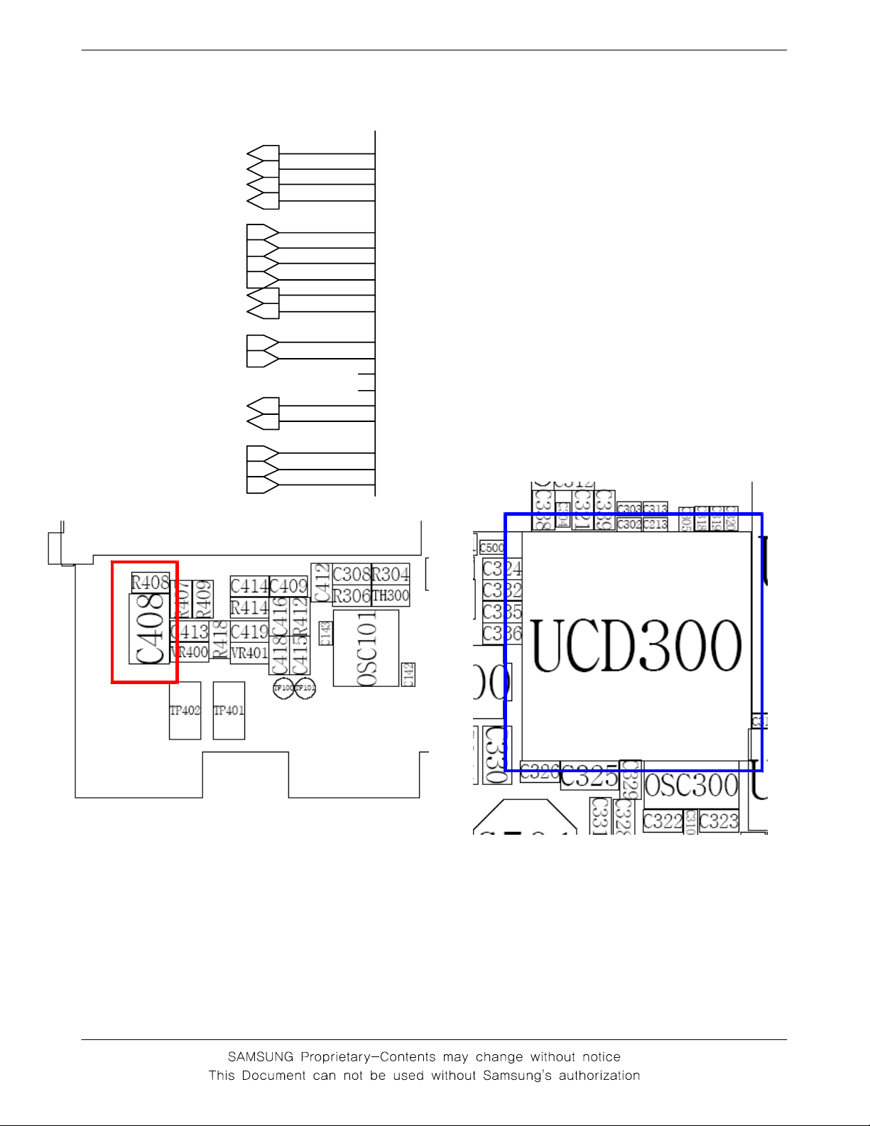
3-1-5.
Microphone Part
M icropho ne doe s not work
Check the
assembled status of
microphone.
Ch eck the referenc e
volta ge on mic pat h
R408=2.4V
Is microphone ok?
END
YES
YES
YES
NO
NO
NO
Rea sse m bl age microp hone
①
resolder or change
(R408, C408)
Check UCD300
MONO1_IN_P
MONO1_IN_N
R412
22K
C415
1000nF
10V
C418
NC
C412
NC
C409
68NF 10V
C414
120PF
50V
C416
68NF
10V
R409
0
R414
0
R418
2.2K,1%
3-13
C413
120PF
50V
C419
120PF
50V
MIC+
MIC-
R407
2.2K,1%
6.3V
33uF
C408
R408
680
VAMICREF
HI_MONO_OUT_N
HI_MONO_OUT_P
LO_MONO_OUT_N
LO_MONO_OUT_P
MONO1_IN_N
MONO1_IN_P
MONO2_IN_N
MONO2_IN_P
MONO_OUT_N
MONO_OUT_P
RADIO_L
RADIO_R
STEREO_OUT_L
STEREO_OUT_R
PWR_KEEP
JIG_ON
PWR_ON
R13
HI_MONO_OUT_N
R14
HI_MONO_OUT_P
R12
LO_MONO_OUT_N
P11
LO_MONO_OUT_P
G13
MONO1_IN_N
J13
MONO1_IN_P
G12
MONO2_IN_N
G11
MONO2_IN_P
N15
MONO_OUT_N
L13
MONO_OUT_P
K15
STEREO1_IN_L
K14
STEREO1_IN_R
H11
STEREO2_IN_L/M
J12
STEREO2_IN_R/M
M14
STEREO_OUT_L
M13
STEREO_OUT_R
P6
PWR_KEEP
E5
PWR_SW2
C4
PWR_SW1N
Flow Chart of Troubleshooting
3-14
Flow Chart of Troubleshooting
3-1-6.
Speaker Part
Speaker does not work
Is th e terminal of
Speaker OK?
YES
Check the
SPK_P & SPK_N
"HIGH"
YES
Check the output c ircuit
of U400(Aud io AMP)
YES
NO
NO
NO
ch eck the sp ecker FPCB
①
Resolder
SPK_P & SPK_N
②
Change or resolder
around U400
③
Check the input c ircu it of
U400(A ud io AMP)
YES
Is speaker OK?
YES
END
NO
Change or resolder
around U400
Change speakerNO
3-15
L403
Flow Chart of Troubleshooting
VBAT
HI_MONO_OUT_P
AMP_EN
C400
C401
R428
R401
R402
R406
R404
A1
VIP
C1 VIM
C404
B1
VDD
U400
A2
VSS
A3VOM
PVSS B3
D
VOP
C3
D
V
N
C
C
P
E
N
N
2
2
12
B
C
R425
C405
R426
L400
L401
C402
C403
R400
R403
RCV-
SPK-
SPK+HI_MONO_OUT_N
RCV+
3-16
 Loading...