How it Works
Log In / Sign Up
Buy Points
How it Works
FAQ
Contact Us
Questions and Suggestions
Users
Samsung
Loading...
S
SGH-I637
4
SGH-I637 Jack
SGH-i637 Series
SGH-i640
SGH-I640V
2
SGH-I667UWAATT
2
SGH-I677
3
SGH-I677DAAATT
SGH-i700
12
SGH-i700 Series
2
SGH-i710
6
SGH-i710 Series
SGH-i7110
10
SGH-i717
5
SGH-I717M
2
SGH-I717R
SGH-I717RWAATT
4
SGH-I717RWZATT
4
SGH-I717ZBAATT
4
SGH-I717ZBZATT
4
SGH-i718
4
SGH-I718 Series
SGH-I727
4
SGH-I727DAAATT
3
SGH-I727MSAATT
3
SGH-I727R
2
SGH-I727ZWAATT
3
SGH-i740
2
SGH-i740c
3
SGH-I747
2
SGH-I747 Galaxy S III
SGH-I747M
4
SGH-I747MBAATT
4
SGH-I747MBBATT
6
SGH-I747MBNATT
5
SGH-I747RWAATT
4
SGH-I747RWBATT
5
SGH-I747ZRBATT
4
SGH-i7500
4
SGH-I750 Series
2
SGH-I757M
SGH-i777
8
SGH-I777ZKAATT
4
SGH-I777ZKZATT
4
SGH-i780
30
SGH-i788
3
SGH-I8000
7
SGH-i8262D
SGH-I827D
SGH-I827ZSAATT
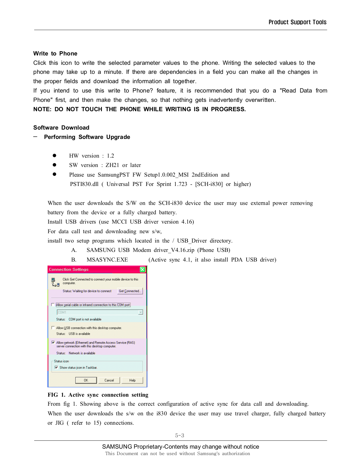
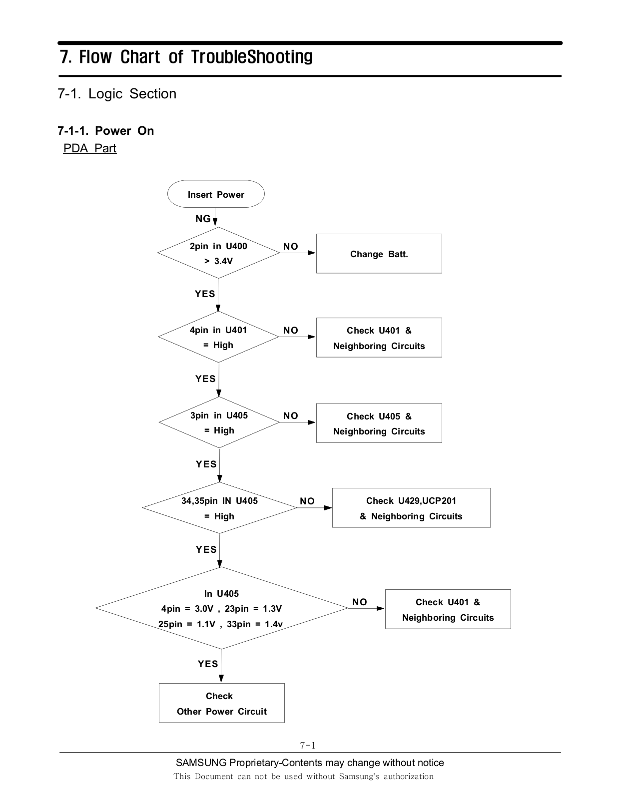
SGH-i830
SGH-I847ZKAATT
SGH-i8510
10
SGH-I857
3
SGH-I857ZAAATT
SGH-I857ZWAATT
SGH-i858 Series
SGH-i8910
8
SGH-I896
2
SGH-I897
3
SGH-I897ZKAATT
2
SGH-I897ZKMATT
SGH-I897ZKZATT
SGH-I900
43
SGH-i9000B
7
SGH-I900C
27
SGH-I900L
3
SGH-I900V
15
SGH-I900 WITU
SGH-I907
8
SGH-i907 Series
2
SGH-I907ZKAATT
2
SGH-i908
2
SGH-i908E
2
SGH-i908L
SGH-I917ZKAATT
SGH-I917ZKBATT
SGH-i9192
SGH-I927R
SGH-I927ZKAATT
2
SGH-I937OKAATT
SGH-I957
3
SGH-I957M
3
SGH-I957ZKAATT
2
SGH-I987
3
SGH-I987ZKAATT
SGH-I997R
SGH-I997ZKAATT
2
SGH-I997ZKMATT
2
SGH-J150
20
SGH-J200
11
SGH-J208
2
SGH-J218
SGH-J400
12
SGH-J408
SGH-J600
11
SGH-J600E
12
SGH-J600G
7
SGH-J600V
SGH-J608
3
Loading...
Loading...
Nothing found
SGH-i830
Service Manual
103 pgs
7.67 Mb
0
Table of contents
Loading...
Samsung SGH-i830 Service Manual
...
Samsung Service Manual
Download
Specifications and Main Features
Frequently Asked Questions
User Manual
Download
Loading...
+
73
hidden pages
Unhide
You need points to download manuals.
1 point = 1 manual.
You can buy points or you can get point for every manual you upload.
Buy points
Upload your manuals
 Loading...