

Samsung SGH-i7110, GT-i7110 Troubleshooting
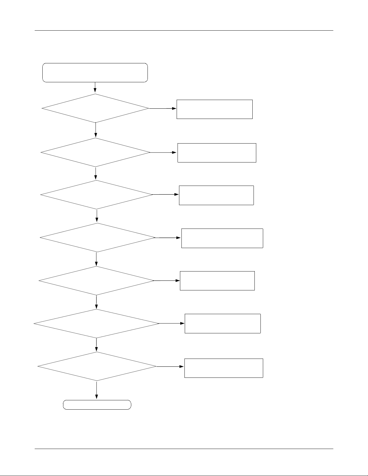
Flow Chart of TroubleShooting
9.
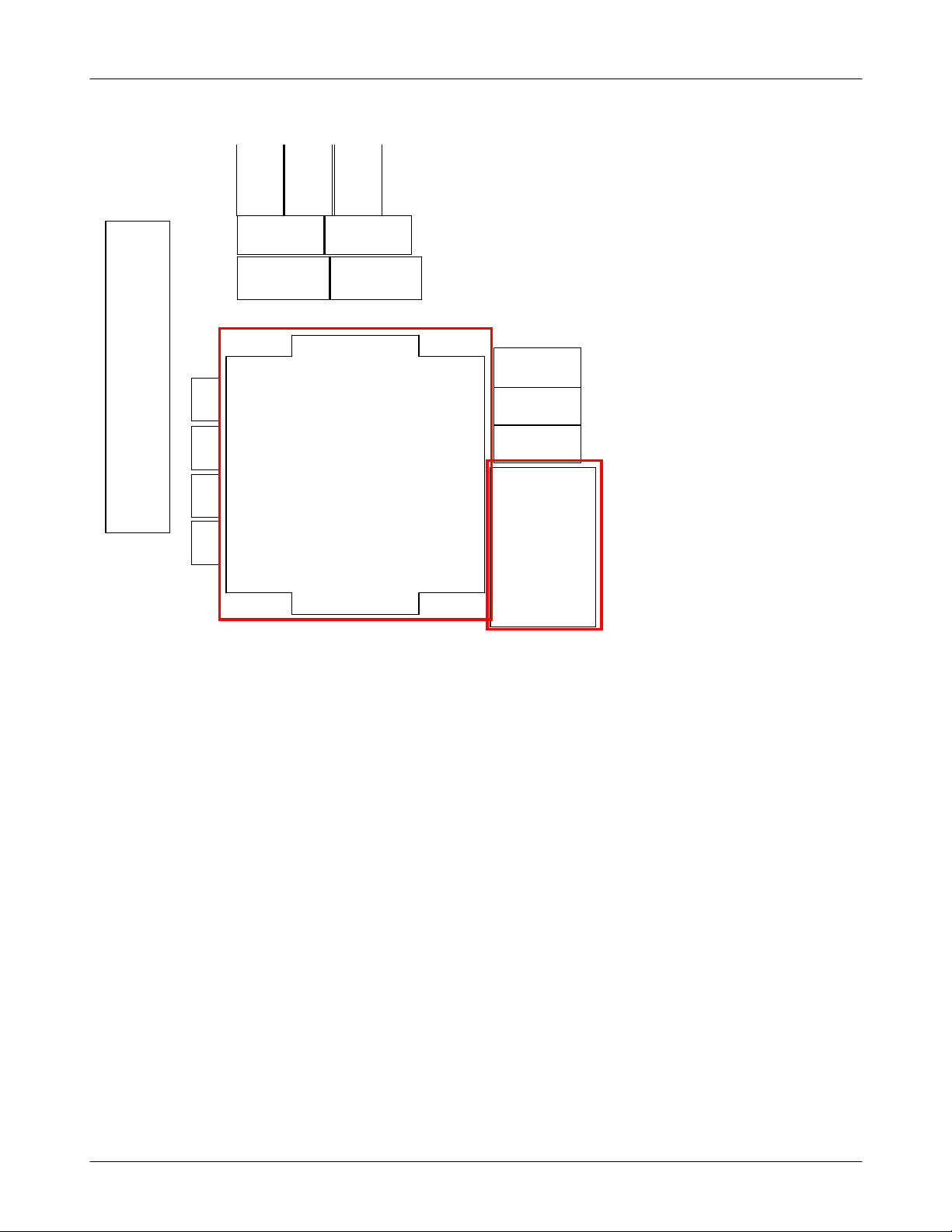
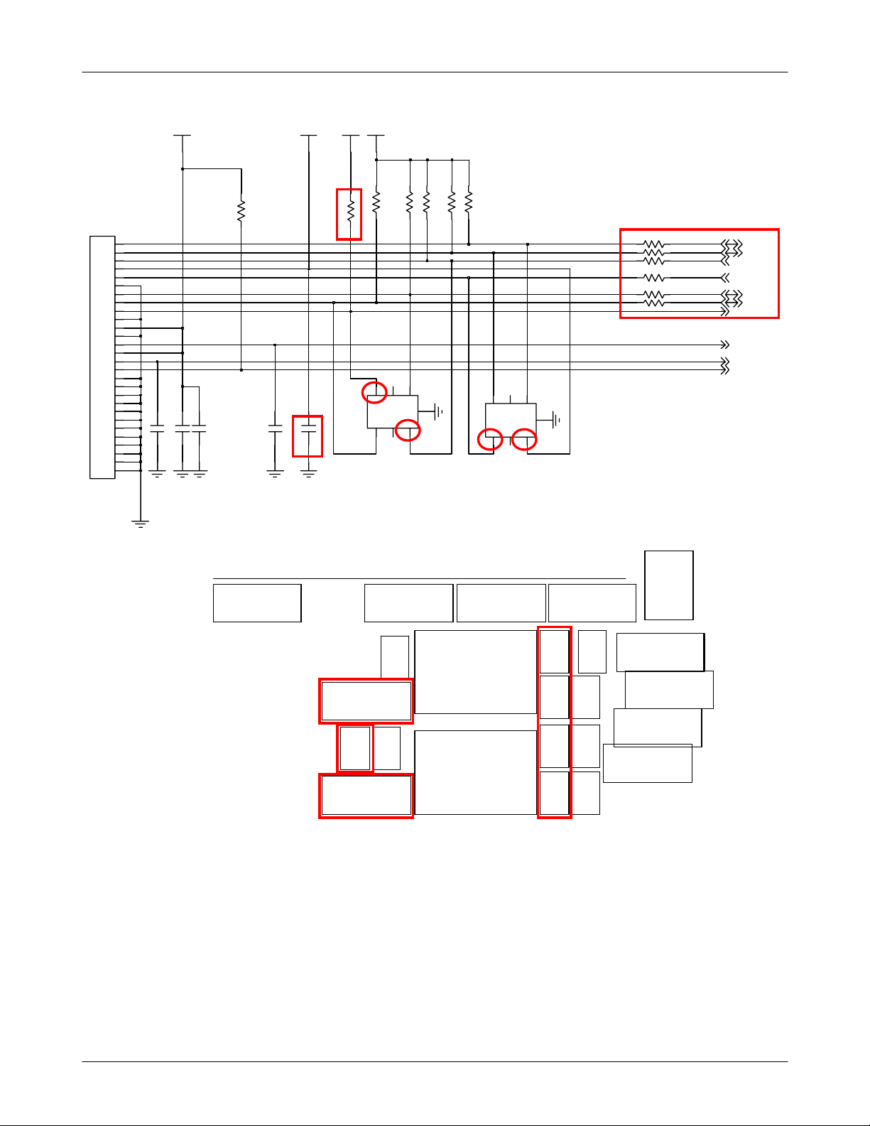
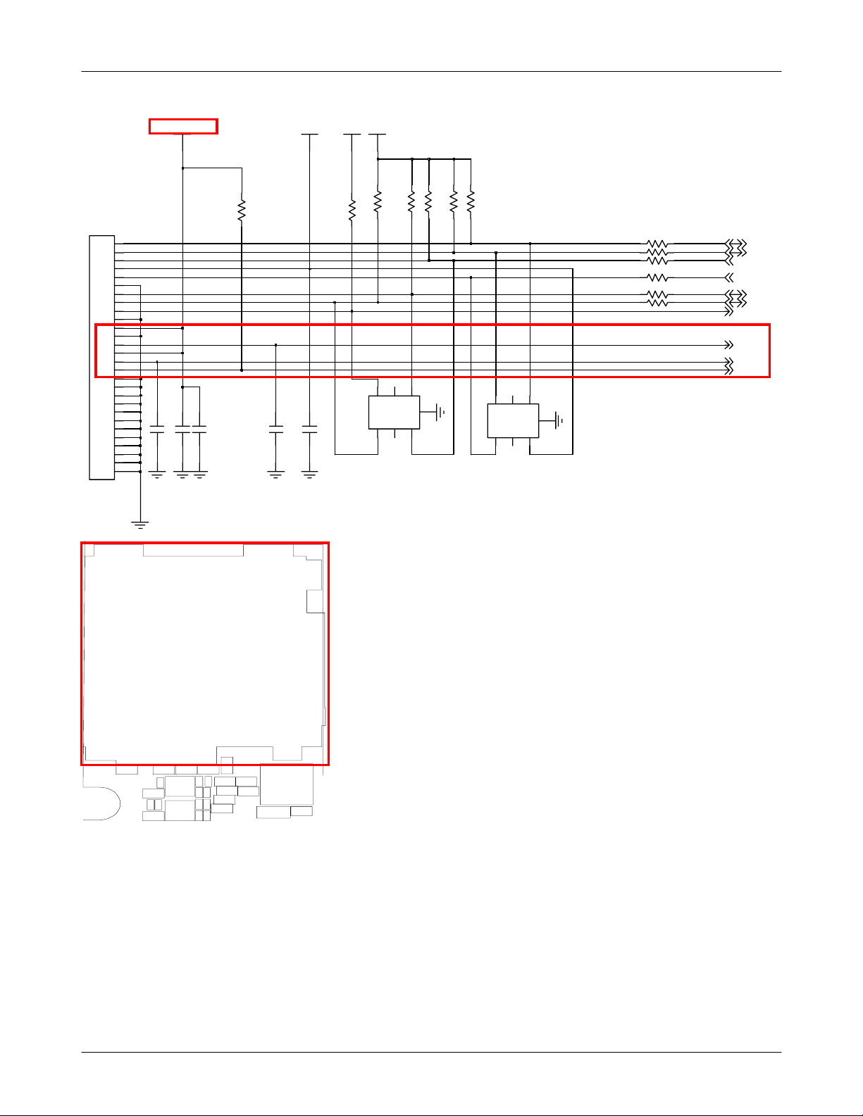
Logic Section
9-1.
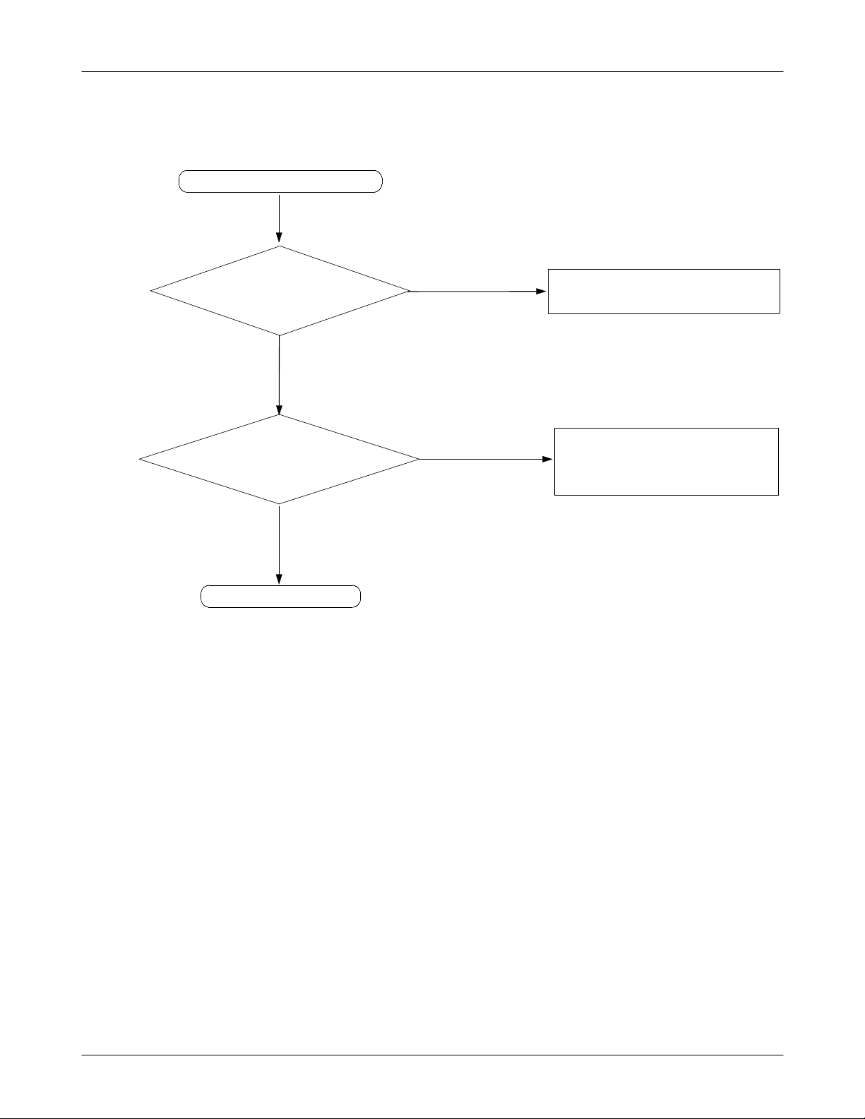
9-1-1 :
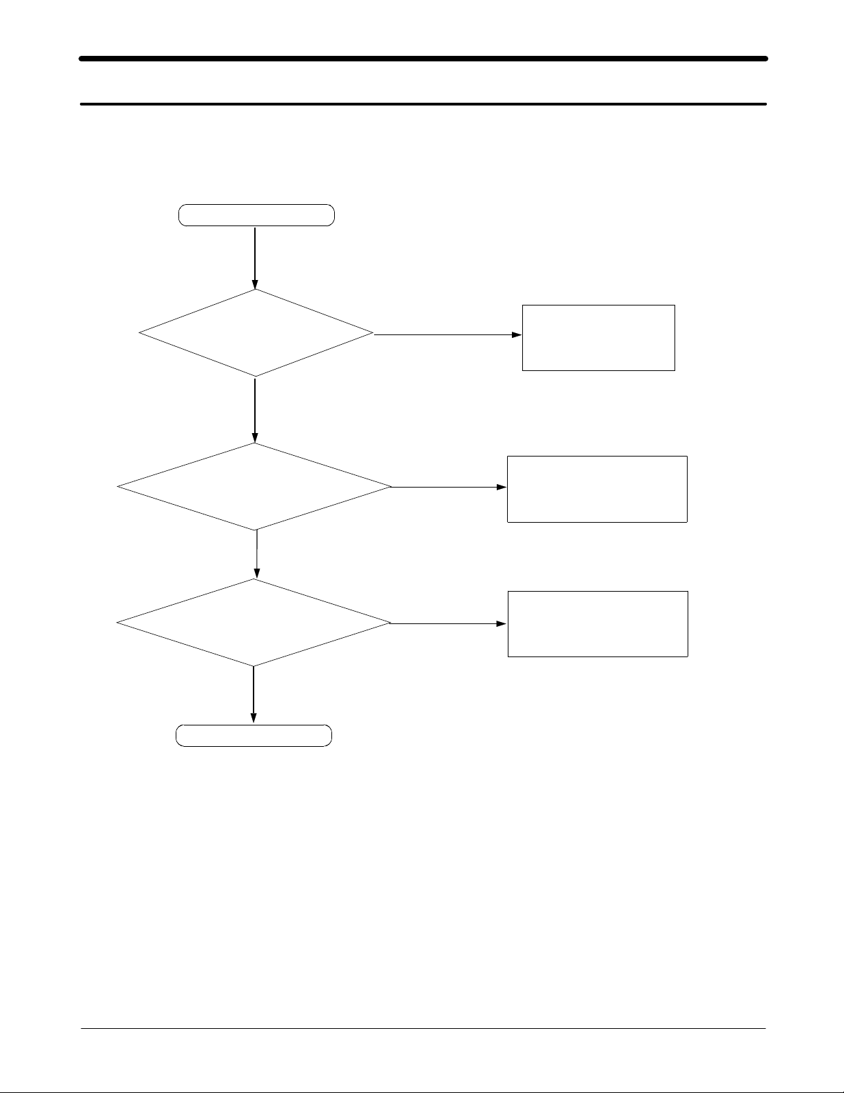
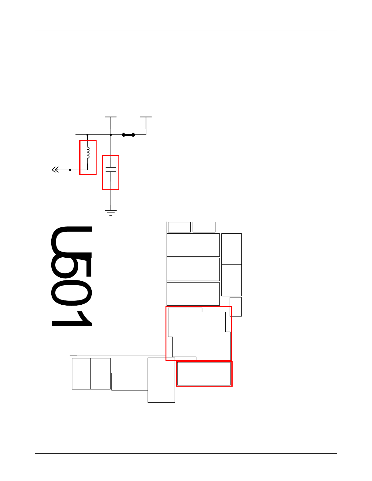
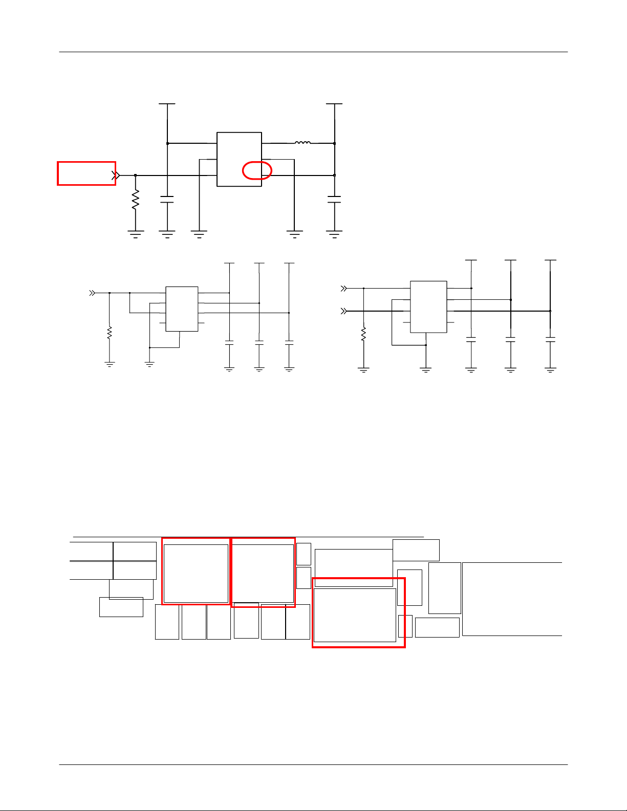
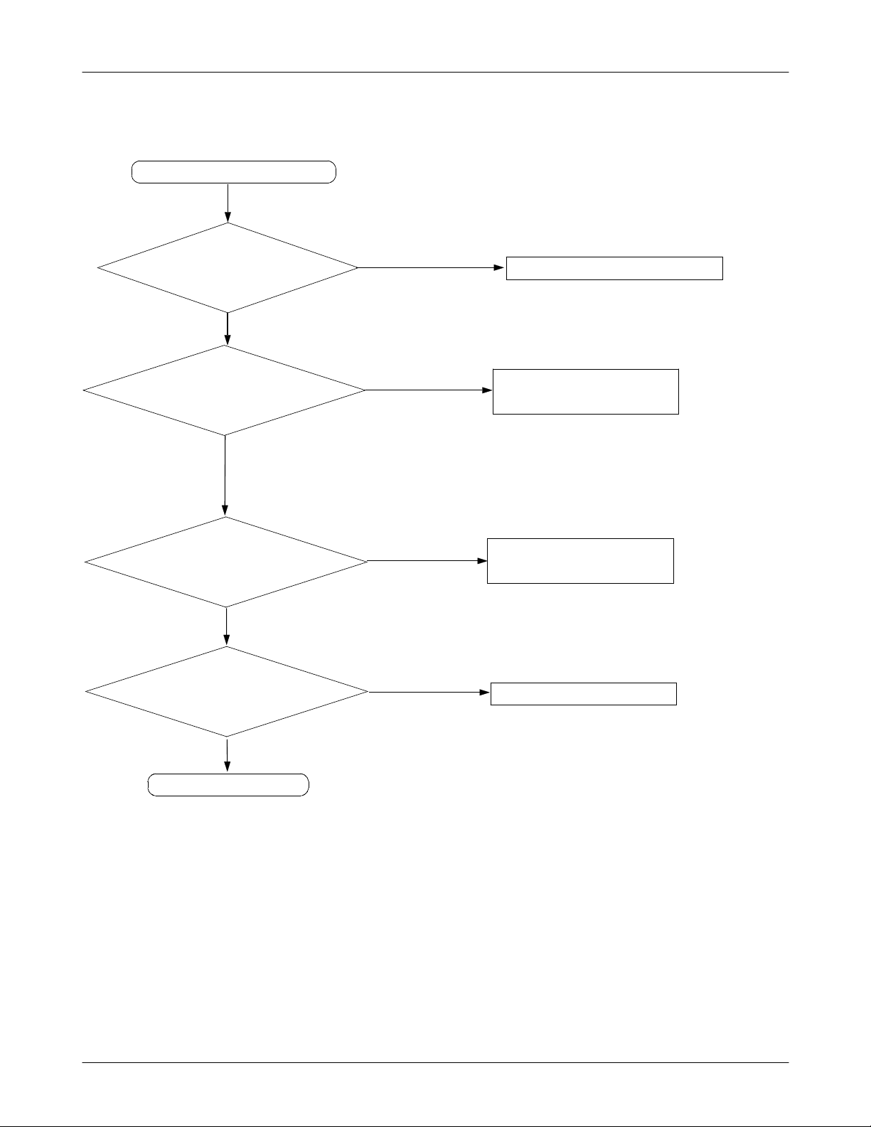
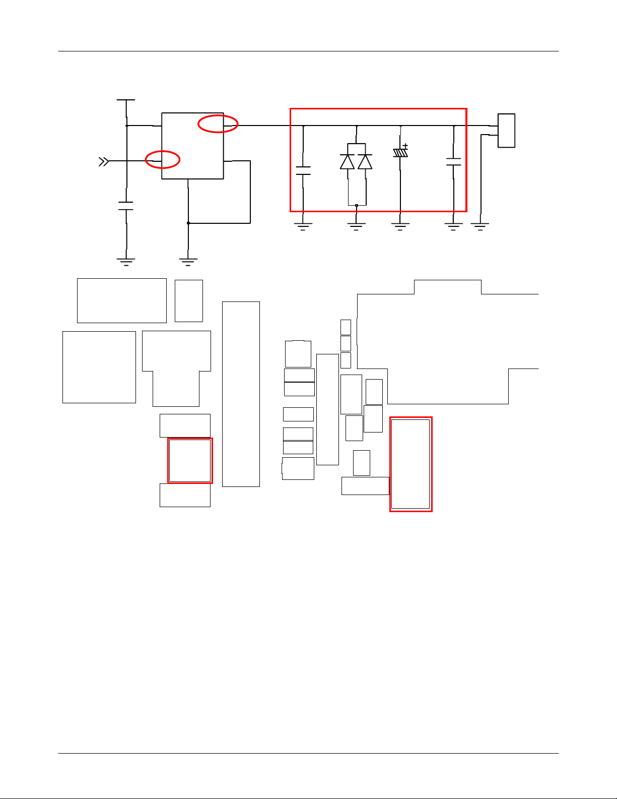
No Power
Press PWR KEY
pin4
U408
output high?
YES
D403 pi
output highV?
n2
NO
NO
Check pin
if One of them is low,
replace board
neighboring circuits or
Replace D403
#1
and
#2
U409 pin
output
>3.5
END
3
V?
YES
NO
neighboring circuits or
Replace U409
9-1
SAMSUNG Proprietary-Contents may change without notice
This Document can not be used without Samsung's authorization
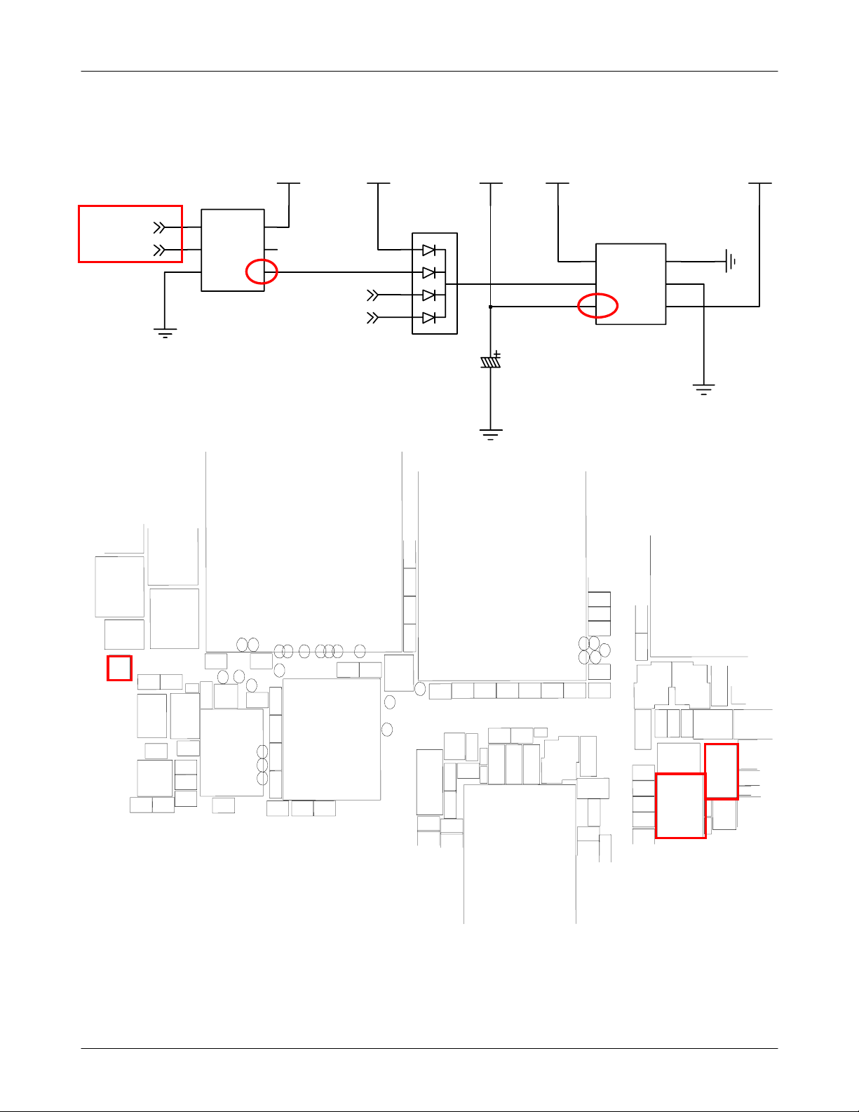
Flow Chart of Troubleshooting
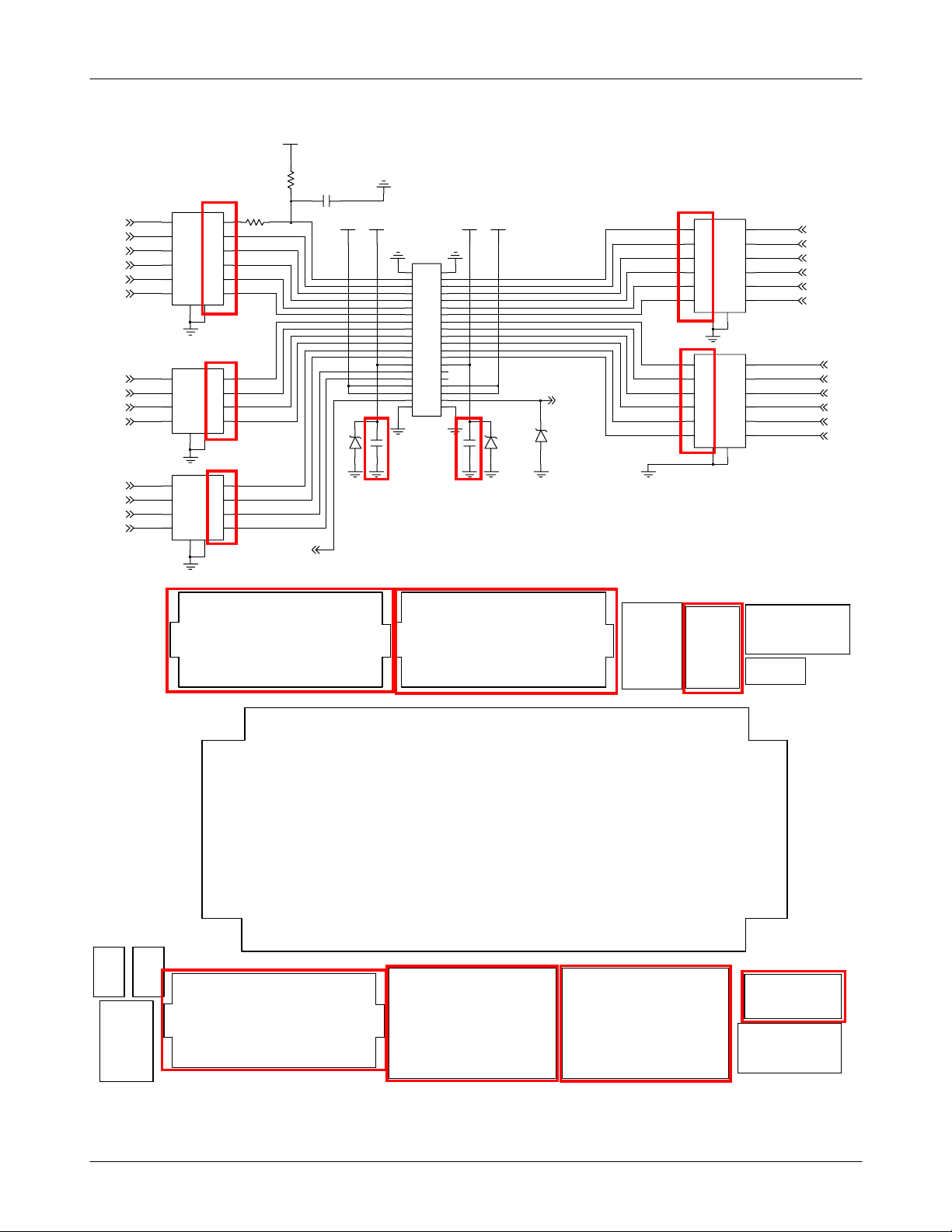
PS_HOLD_PU30
SYSEN30
C
7
1
9
4
8
U
0
C
3
0
7
L
C
U
6
1
0
9
0
4
6
1
4
R
3
2
4
R
0
0
4
L
C
3
4
C
Q
R
R
5
0
4
U
V_BAT
C
C
R
R
0
4
0
4
4
3
3
3
4
4
1
0
4
4
0
1
1
4
C
8
0
4
C
4
4
0
4
U
2
U
3
C
6
1
1
0
9
5
3
C
5
C
C
1
S
4
5
O
C
4
4
5
C
1
3
5
C
VBAT
C
P
1
3
0
C
1
1
5
0
0
3
3
U
R
9
5
2
U
9
C
8
0
5
R
6
0
5
R
3
3
C
4
5
5
C435
5
0
5
C
7
4
5
C
0
3
R
0
3
5
0
4
5
C
0
4
1
5
C
0
0
3
C
7
2
3
4
5
C
1
1
3
C
1
C2
2
C1
3
OUT VIN
C
0
3
C
0
3
C
0
3
R
3
3
C
1
3
R
1
2
0
0
3
3
E
E
D
D
O
O
M
M
0
0
0
3
0
E
3
D
P
O
T
M
1
3
C
0
3
R
3
0
9
7
6
0
5
5
C
L
5
C
5
3
2
5
C
3
6
5
C
U409
6
GND
5
C3
4
1
3
3
3
4
0
4
4
2
UT
O
_
X
U
M
A
6
8
0
4
C
7
0
4
C
5
2
U
4
C
1
1
4
R
8
1
4
0
0
4
L
7
1
4
C
4
L
4
9
1
4
C
0
0
4
1
4
C
C
2
4
C
C
4
3
5
2
5
4
8
3
3
5
C
C
8
5
6
C
7
5
0
C
U
1
5
1
C
6
7
5
3
C
1
5
C
5
1
5
C
4
0
D
9
ON_SW
0
0
3
S
C
_
D
S
9
0
R
9
V_EXT_FET
0
0
3
E
M
U
E
0
W
0
_
3
D
S
A
7
0
9
R
2
0
5
D403
1
3
4
5
2
1
3
C
7
1
3
C
7
1
3
R
0
1
2
0
3
P
T
0
R
9
3
R
4
3
0
0
U
M
A
R
P
D
_
T
N
I
n
E
V
I
T
C
A
_
A
D
P
M
A
R
P
D
_
S
C
n
3
R
8
C
5
1
8
C
5
4
V2DD6_100 VREG_TCXO_2.85V
U408
1
A
2
B
3
GND
VCC
NC
6
5
4
Y
IF_CON_SENSE
2
0
7
U
2
0
7
L
3
R
6
0
6
C
0
7
6
6
0
C
6
0
R
1
2
0
6
R
4
0
6
1
U
0
0
6
C
5
0
2
U
1
1
6
C
0
6
0
0
6
R
U
0
6
C
9
1
6
0
C
5
1
4
1
9
R
9
9
NC
Y
S
_
M
C
P
1
1
0
4
Q
0
0
E
L
A
_
D
N
A
N
E
R
_
D
N
A
N
C
N
I
D
_
M
C
P
9
C
5
_N
T
U
O
S
E
R
2
3
1
1
U
T
O
D
_
M
C
P
K
L
C
_
M
C
P
E
V
I
T
C
A
_
E
N
O
H
P
S
S
3
A
A
0
C
R
3
_
_
P
D
D
T
S
S
8
7
0
7
P
T
2
0
9
C
1
0
9
C
3C
0
9
U
C
4
0
9
0
3
9
R
6
0
9
R
9-2
SAMSUNG Proprietary-Contents may change without notice
This Document can not be used without Samsung's authorization
Flow Chart of Troubleshooting
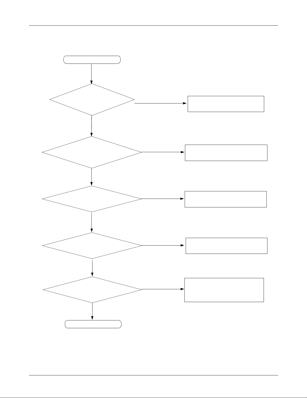
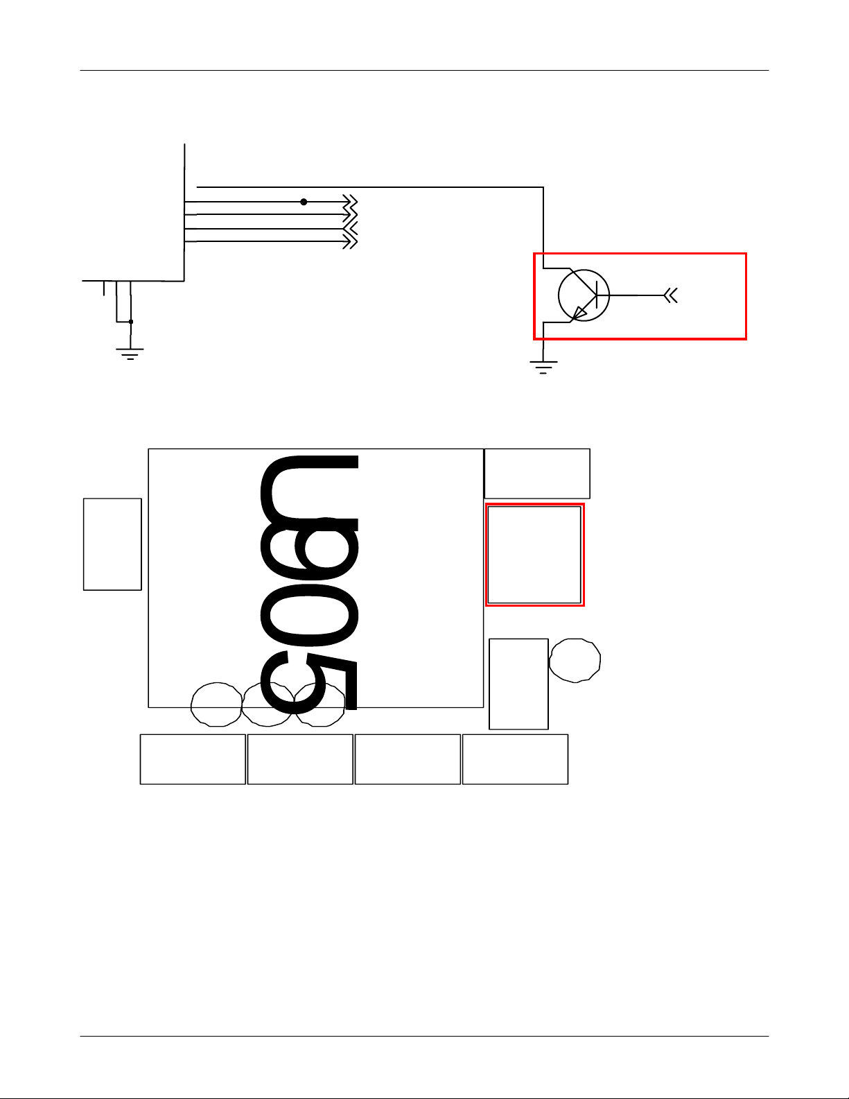
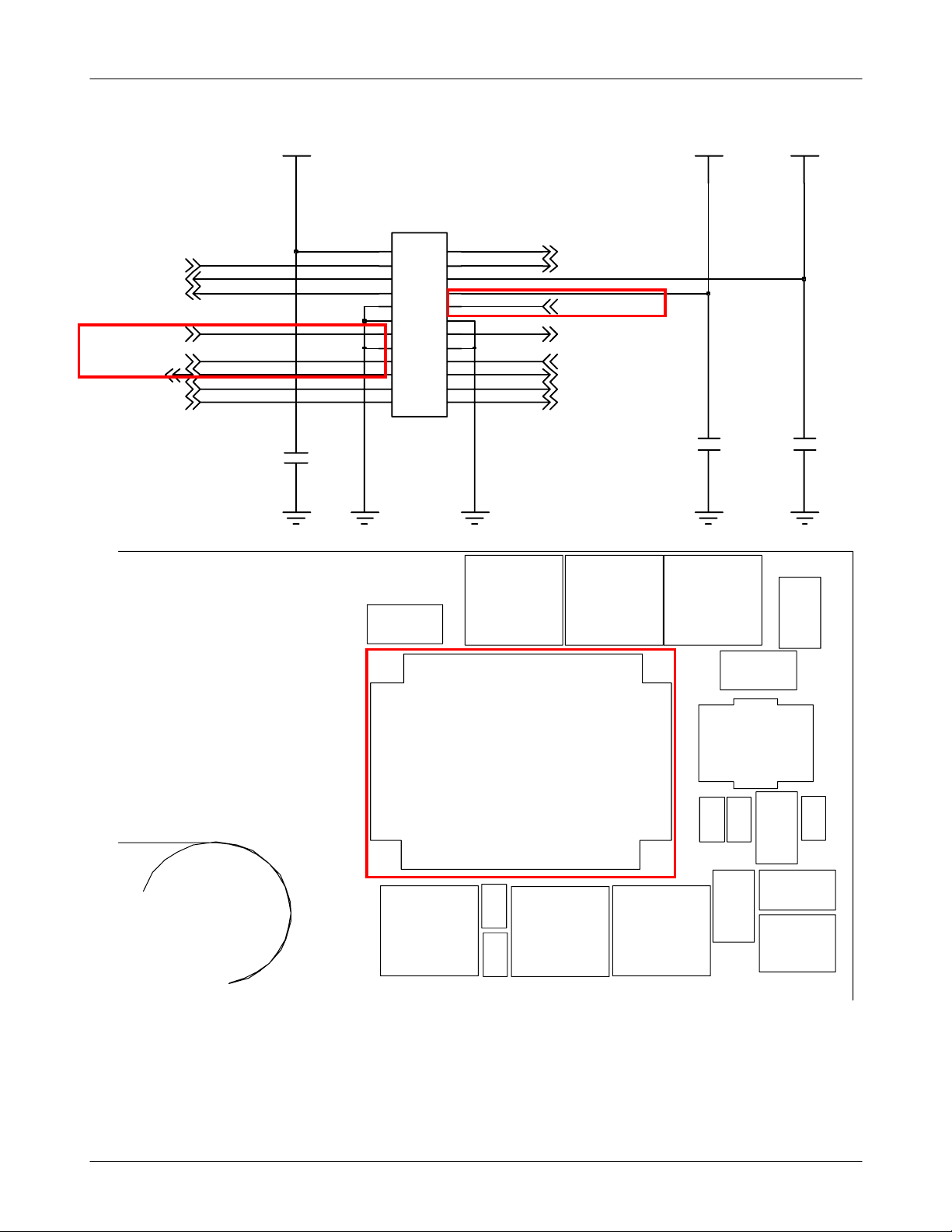
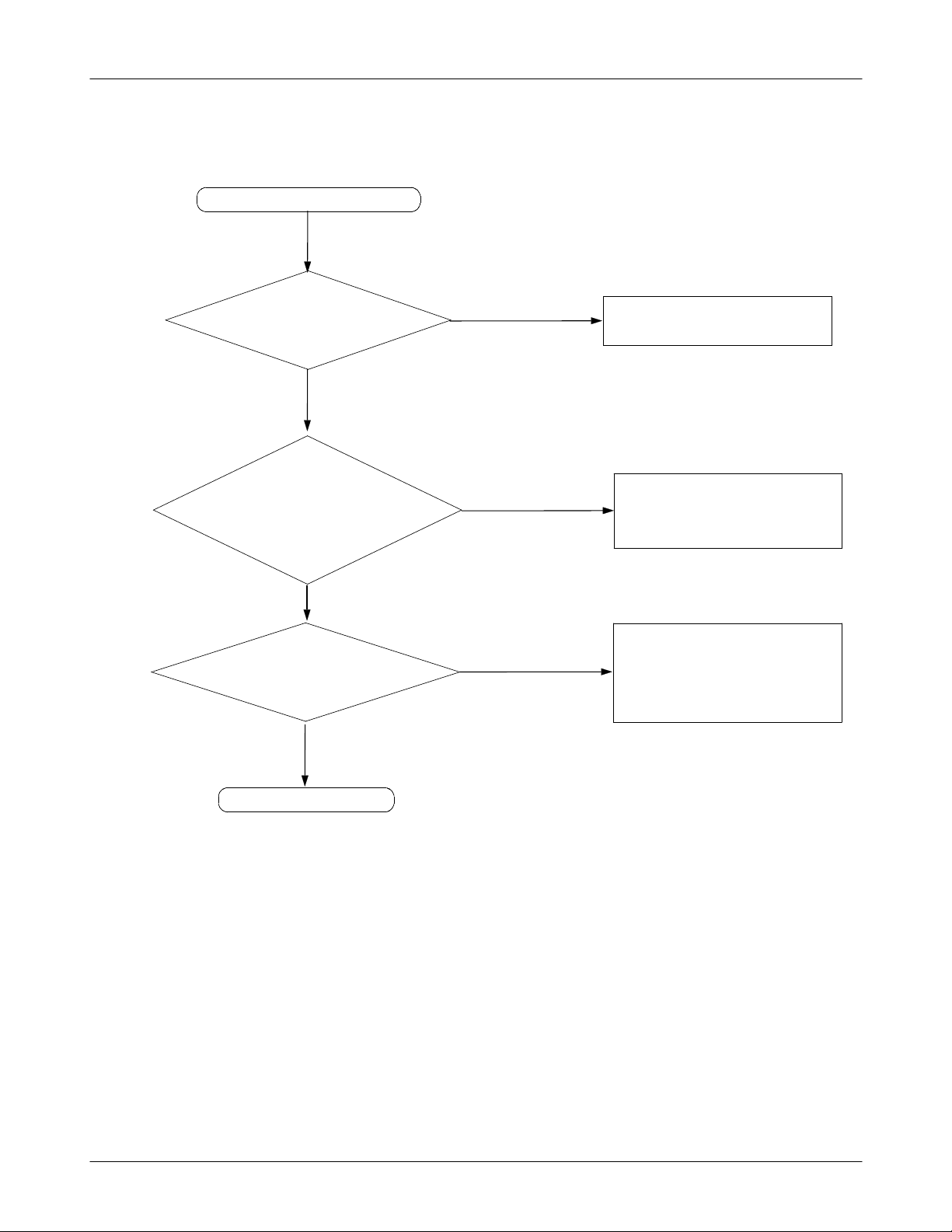
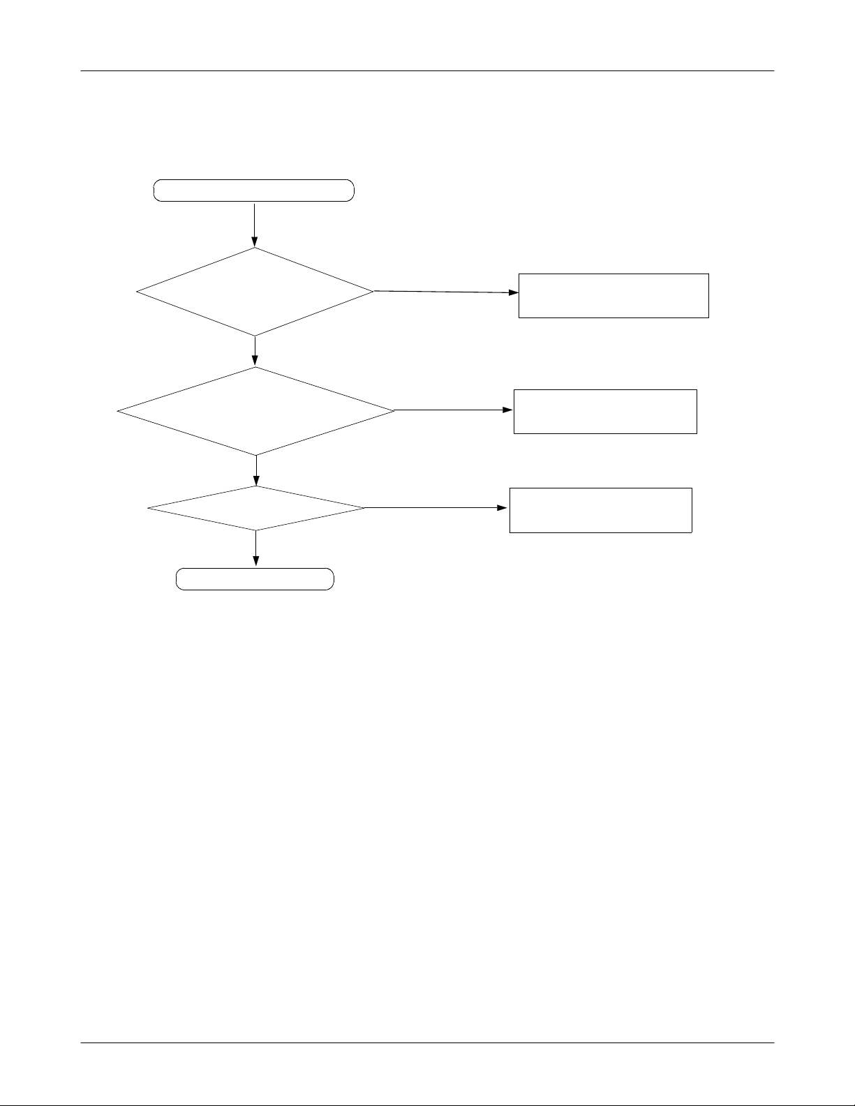
9-1-2 :
Abnormal initial operation(Normal
Press PWR KEY
MOD200 pin
is exist?
voltage level
C552
= 1.1~1.3
voltage level
C569
=1.8
40
YES
V?
YES
V?
+4.0V
NO
NO
NO
voltage source)
Check OSC
neighboring circuits
Check
Check
and neighboring
L504
circuits
and neighboring
L507
circuits
501
and
YES
Q401 pin3
output isasserted?
YES
pin4
U301
output isasserted?
YES
END
NO
NO
Check Q401
and neighboring circuits
Check
and neighboring circuits
if necessary change the board
U301
9-3
SAMSUNG Proprietary-Contents may change without notice
This Document can not be used without Samsung's authorization
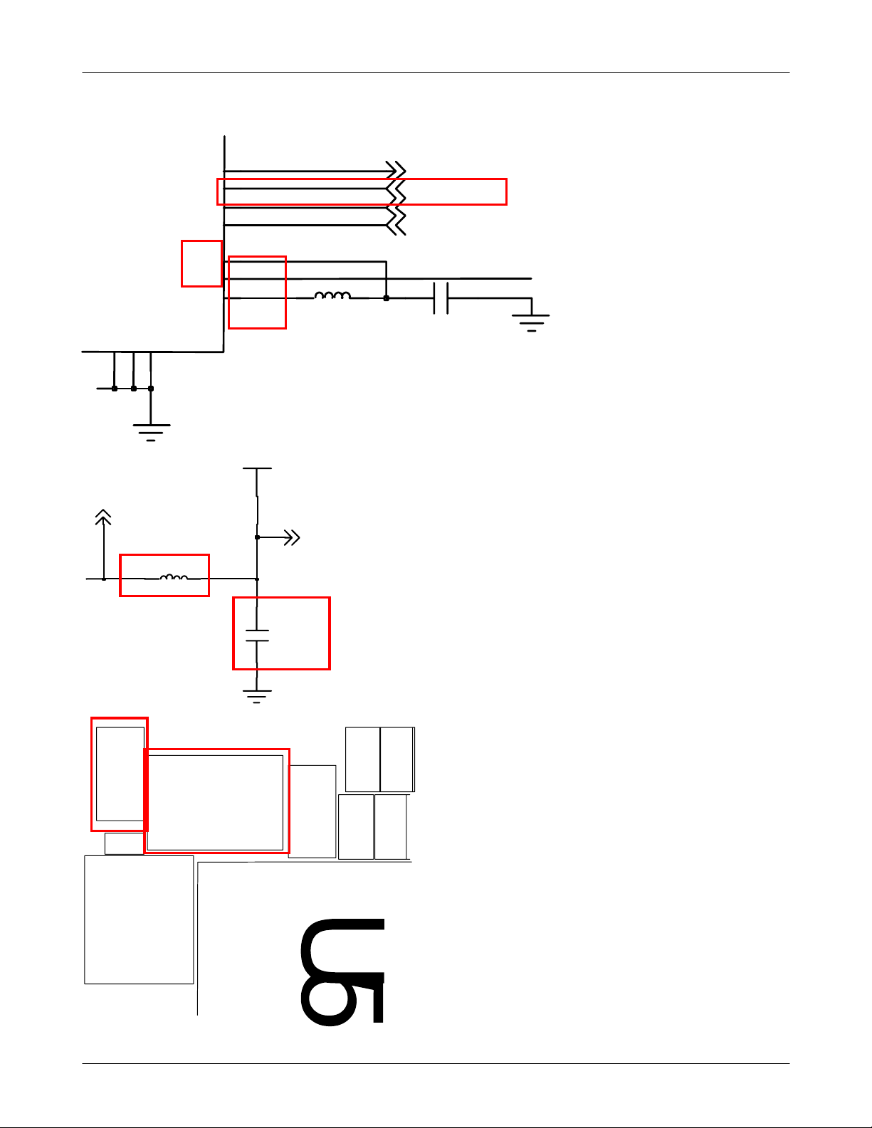
Flow Chart of Troubleshooting
BT_CTS
CLK_REQ
FAST_CLK_IN
SLOW_CLK_IN
PMEN|WLAN_RESETX
VFB
VIO
VSW
D
D
D
N
N
N
G
G
G
2
1
0
5
5
5
L
_
1
D
D
V
L504
5
18
40
14
16
29
13
VDD1_1.35V
WLAN_CLK_REQ
WLAN_CLK_IN
32KCLKOUT
WLAN_PMEN
C226
L213
VDD1_OUT
C
5
5
2
C505
O
S
C
5
0
0
C526
L504
R509
WARM_RES
C552
C
5
5
3
C
5
3
5
C
5
2
4
C
5
4
8
C
5
3
1
9-4
SAMSUNG Proprietary-Contents may change without notice
This Document can not be used without Samsung's authorization
Flow Chart of Troubleshooting
VIO_L
VIO
7
0
5
L
9
6
5
C
V1DD8
R506 R508
C
5
C547
4
5
C
C540
5
3
0
C543
C
5
2
7
C
5
3
6
L507
C
5
3
2
C533
SAMSUNG Proprietary-Contents may change without notice
This Document can not be used without Samsung's authorization
C
5
5
8
C569
9-5
Flow Chart of Troubleshooting
HSET_BIAS
KPD_PWR_N
MSM_INT_N
PON_RESET_N
PS_HOLD
SLEEP_CLK
C
C
C
N
N
N
D
1
1
2
1
D
C
9
1
0
K1
L4
C10
G10
F10
K9
TP400
PM_INT_N
PON_RESET_N
MSM_PSHOLD
SLEEP_CLK
3
2
R914
Q401
1
Q401
FONE_ON30
PHONE_ACTIVE
PCM_CLK
PCM_DOUT
C
9
PCM_DIN
1
1
C901C902C903C904
9-6
SAMSUNG Proprietary-Contents may change without notice
This Document can not be used without Samsung's authorization
U301
Flow Chart of Troubleshooting
V2DD6_100
PON_RESET_N
nMSM_RST30
C
5
5
3
C
5
3
5
C
5
2
4
C
5
4
8
C
5
3
1
C
5
1
8
C
5
4
4
1
A
2
B
3
GND
VCC
NC
6
5
4
Y
R305
OSC501
C541
C539
C
5
2
9
R506 R508
C547
C540
C543
U301
R305
FONE_RST
C
5
4
5
C
5
3
0
C
5
2
7
L507
9-7
SAMSUNG Proprietary-Contents may change without notice
This Document can not be used without Samsung's authorization
Flow Chart of Troubleshooting
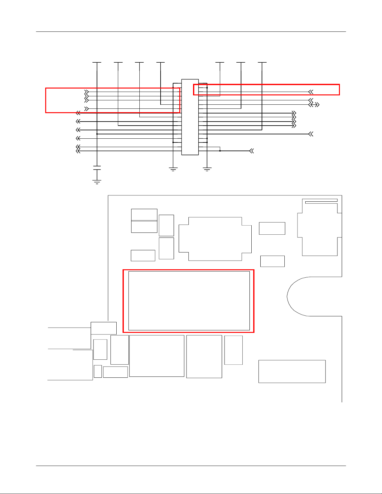
9-1-3 :
Abnormal5M,CIF Camera operation
Drive Camera
pin
U605
U606 pin6,8
&
&U607
output Exist?
CIF) HDC601
(
pin9,14,18,22
M) HDC602
(5
pin5,6,9,13
output exist?
pin6
YES
3
,8
NO
NO
Check
and neighboring circuit
U605 , U607
U606 EN#(high?)
,
Check UCP
neighboring circuit
800
and
YES
R802, R803
I2C Clk, Data
output exist?
YES
Is Camera okay?
YES
END
SAMSUNG Proprietary-Contents may change without notice
This Document can not be used without Samsung's authorization
9-8
NO
NO
Check UCP
neighboring circuit
Change the Cam. module.
800
and
Flow Chart of Troubleshooting
CAM_PWR_EN1
CAM_PWR_EN3
R604
R603
V_BAT
1
CE1
2
GND
3
CE2
4
NC
C613
U606
9
VOUT1
VDD
VOUT2
D
NC
N
G
VCAM_12C
U605
1
6
IN
5
4
8
7
6
5
GND
_SHDN
VCAM_28AF
GND
C617
LX
V_BAT
L600
2
3OUT
C612
VCAM_18IO V_BAT VCAM_28D
8
7
VDD
6
5
D
NC
N
G
C616
C619
C614
C618
VCAM_28A
CAM_PWR_EN2
CAM_PWR_EN3
C615
R605
U607
1
CE1
VOUT1
2
GND
3
CE2
VOUT2
4
NC
9
R519
R517
C559
C566
C565
C560
5
U606 U607
0
6
R
4
0
L60 0
6
R
C612
5
4
8
5
1
6
C
SAMSUNG Proprietary-Contents may change without notice
This Document can not be used without Samsung's authorization
1
6
C
7
1
6
C
1
6
C
9
1
6
C
6
1
6
C
9-9
0
6
U
3
0
6
R
3
1
6
C
R915
9
0
9
C
6
0
9
U
Flow Chart of Troubleshooting
QCIF_STBY
CAM_D0_CIF
CAM_D1_CIF
PIXEL_PCLK_CIF
PIXEL_VSYNC_CIF
SDA1
PIXEL_HSYNC_CIF
CAM_RST
VCAM_28A
3
2
6
C
HDC601
2
2
4
4
6
6
8
8
10
10
12
12
16
18
20
22
24
11
13
1414
16
15
1718
20
19
22
21
24
23
C623
VCAM_18IO
1
1
3
3
5
5
7
7
9
9
11
13
15
17
19
21
23
U
6
1
1
CAM_D3_CIF
CAM_D2_CIF
PIXEL_MCLK_CIF
CAM_D4_CIF
SCL1
CAM_D5_CIF
CAM_D6_CIF
CAM_D7_CIF
U
6
1
2
2
2
6
C
U
6
1
3
DVDD_1.8V
4
2
6
C
R
5
1
2
H
BH302
U
6
1
4
D
C
6
0
1
C
6
2
2
C
6
2
0
U
6
1
0
U
6
1
5
R511
U
5
0
3
C
R
5
5
1
7
0
0
C
6
2
4
C
C
5
5
7
4
1
6
C621
U
6
0
8
9-10
SAMSUNG Proprietary-Contents may change without notice
This Document can not be used without Samsung's authorization
Flow Chart of Troubleshooting
PIXEL_MCLK
5M_STBY
PIXEL_HSYNC
PIXEL_VSYNC
CAM_D1
CAM_D5
CAM_D7
FLASH_FB_B
FLASH_FB_A
C629
VCAM_28D
ZD601
ZD600
C629
HDC602
1
3
5
78
9
11
13
15
17
19
21
23
25
27
29
33 34
3
0
6
D
Z
2
0
CN500
6
D
Z
1
3
566
7
9
111212
131414
151616
171818
19
21 22
23 24
25 26
27
29
313132
33
2
2
4
4
8
10
10
20
20
22
24
26
28
28
30
30
32
34
VCAM_28AFVCAM_12CDVDD1_1.8V VCAM_18IO VCAM_18IOVCAM_28A
FLASH_OUT
D202
C223
CAM_D0
CAM_D2
CAM_D4CAM_D3
CAM_D6
PIXEL_PCLK
SCL1
SDA1
CAM_RST
2
0
2
T
N
A
L60 0
5
0
6
U
C612
3
1
6
C
3
0
6
R915
R
9
0
9
C
6
0
9
U
2
0
6
C
D
H
0
0
9
L
8
0
9
C
L70 0
9-11
SAMSUNG Proprietary-Contents may change without notice
This Document can not be used without Samsung's authorization

SCL1
SDA1
Flow Chart of Troubleshooting
VIO
R802 R803
C707
C708
D702
C802
R
8
0
7
R
8
0
9
C815
C805
C822
R802
R803
C801
FM_IN T
C
8
1
1
R
8
0
0
PWRON_RES
R
8
0
4
C
8
R
1
9
1
8
6
C
8
1
6
C
8
2
8
C
8
1
7
C
8
2
9
R
8
1
2
R
8
0
6
UCP800
C
8
2
4
R
9
1
7
CLK80 0
C
8
2
0
U
6
1
6
C
6
2
8
R
9
0
2
nDPRAM_CS
gpmc_a90 0
nDPRAM_INT
R
9
0
1
C
8
2
1
C
8
2
7
C
8
0
9
C
8
1
9
C
8
2
6
R
9
0
8
C
8
0
4
C
8
1
2
C806 C807
C814
SAMSUNG Proprietary-Contents may change without notice
This Document can not be used without Samsung's authorization
C823
C813
C800
9-12
R801
C803
C825
C810
C808
Flow Chart of Troubleshooting
9-1-4 :
Abnormal3X4 KEY operation
Press the key
KBR# level
goes high to low?
YES
KBC# level
goes low to high?
END
NO
NO
Check idle state level
and neighboring circuit
Check idle state level
and neighboring circuit
if necessary change the board
KBC0
KBC1
KBC2
KBC3
KBC4
KBC5
KBC6
F700
1
F1
2
F2
3
F3
4
F4
5
F5
6
F6
7
F7
8
F8
GND
17
VBB_D_2.9V
V_BAT
HDC700
16
F1
15
F2
14
F3
13
F4
12
F5
11
F6
10
F7
9
F8
MOUSE_MOTION_2.9V
MOUSE_SHDN_2.9V
ON_SW
0
2
0
0
7
R
0
0
7
7
C
C
2
1
2
1
4
3
4
3
5
6
56
8
7
8
7
9
10
10
9
11 12
12
11
13
14
13 14
16
15
16
15
17
18
18
17
19
20
20
19
21
2222
21
23 24
24
23
0
0
7
D
VCC_KEY_3.3V
1
0
7
D
KBR0
KBR1
KBR2
KBR3
MOUSE_CLK_2.9V
MOUSE_nCS_2.9V
MOUSE_TXD_2.9V
MOUSE_RXD_2.9V
MMICP
MMICN
4
3
5
6
0
0
0
0
7
7
7
7
C
C
C
C
9-13
SAMSUNG Proprietary-Contents may change without notice
This Document can not be used without Samsung's authorization
Flow Chart of Troubleshooting
S
C
2
0
6
C
5
1
3
L
5
0
1
L
5
0
0
C502C508
D700D701
C
7
0
3
C
7
0
4
C
7
0
HDC700
5
C
7
0
6
C702
R700
C700
F
7
0
0
9-14
SAMSUNG Proprietary-Contents may change without notice
This Document can not be used without Samsung's authorization
Flow Chart of Troubleshooting
9-1-5 :
Abnormal LCD operation
Press Power key
Check LCD
connector
Normal
Check C721 and
C722 value exist?
YES
Check
output exist?
F701~
F705
abnormal
NO
NO
Reconnect LCD Connector
Resolder C721,C722
and neighboring circuit
Check UCP
and neighboring circuit
800
YES
Is LCD module
okay?
YES
END
NO
Change LCD Mod.
9-15
SAMSUNG Proprietary-Contents may change without notice
This Document can not be used without Samsung's authorization
Flow Chart of Troubleshooting
VLCD18
1
0
7
R
F701
12
10
GND
R709
OUT1
11
OUT2
10
OUT3
9
OUT4
8
OUT5
7
OUT6
GND
F703
1
IN1
2
IN2
3
IN3
4
IN4
F705
1
IN1
2
IN2
3
IN3
4
IN4OUT4
LCD_CHANGE
1
8
7
6
5
8
7
6
5
2
3
4
5
6
IN1
IN2
IN3
IN4
IN5
IN6
OUT1
OUT2
OUT3
OUT4
OUT1
OUT2
OUT3
GND
13 14
GND GND
9
GND
910
MLCD_RST
LCD_DE
LCD_PCLK
LCD_HSYNC
LCD_D(0)
LCD_D(2)
LCD_D(4) LCD_D(7)
LCD_D(6)
LCD_D(8)
LCD_D(10)
LCD_D(12)
LCD_D(14)
LCD_D(16)
LCD_D(17)
C712
ELVDD_4.6V
VLCD18
6
0
6
D
Z
ELVSS_-5.4V
2
1
4
3
5
6
78
9
10
11 12
13
14
15 16
17
18
19
20
21
22
24
23
25
26
27 28
29
30
32
31
33
34
35 36
37
38
40
39
VLCD30
2
4
6
8
10
12
14
16
18
20
24
28
30
32
36
40
5
2
0
2
6
7
D
C
Z
EL_ON
4
0
6
D
Z
HDC701
1
3
5
7
9
11
13
15
17
19
21 22
23
25 26
27
29
31
33 34
35
37 38
39
1
2
7
C
1
IN1
2
IN2
3
IN3
4
IN4
5
IN5
6
IN6
1
IN1
2
IN2
3
IN3
4
IN4
5
IN5
6
IN6
GND14GND
13
GND
13 14
12
OUT1
11
OUT2
10
OUT3
9
OUT4
8
OUT5
7
OUT6
F702
12
OUT1
11
OUT2
10
OUT3
9
OUT4
8
OUT5
7
OUT6
GND
F704
LCD_VSYNC
DISPLAY_CS
DISPLAY_CLK
DISPLAY_SI
LCD_D(1)
LCD_D(3)
LCD_D(5)
LCD_D(9)
LCD_D(11)
LCD_D(13)
LCD_D(15)
R
7
0
1
C
7
1
2
F702
R
7
0
9
F701
F704
H
D
C
7
0
1
F703
F705
Z
D
6
0
5
C
7
2
2
ZD606
ZD604
R702
C721
9-16
SAMSUNG Proprietary-Contents may change without notice
This Document can not be used without Samsung's authorization
Flow Chart of Troubleshooting
9-1-6 :
Abnormal T-Flash operation
Insert the card
R417,
R425~
R429~
,
Check
C434
exist
value
?
YES
R427
R431
NO
NO
Resolder R417,C434
and check neighboring circuit
Resolder
R429~
,
R425~
R427
R431
and neighboring circuit
CD400 pin
output exist?
END
YES
3,4,5,9
YES
NO
Check D404,D405
and neighboring circuit
if necessary change the
board
9-17
SAMSUNG Proprietary-Contents may change without notice
This Document can not be used without Samsung's authorization
Flow Chart of Troubleshooting
CD400
1
2
3
4
5
6
7
8
9
10
11
12
13
14
15
16
NC
NC
NC
NC
NC
NC
NC
NC
NC
NC
NC
NC
1
2
3
4
5
6
7
8
9
10
11
12
13
14
15
16
17
18
19
20
21
22
23
24
25
26
27
28
VREG_USIM_2.85V
1
3
3
3
4
4
C
C
VTF_3.0V
4
2
4
R
2
0
3
4
C
4
3
3
4
4
C
C
V1DD8
7
1
4
R
VTF_3.0V
8
1
4
R
6
1
O
I
O
I
D404
1
0
9
1
4
R
4
5
V
O
I
5
D
N
G
C
O
I
N
2
3
2
2
2
2
4
4
4
R
R
R
5
4
6
V
O
O
I
I
O
I
1
2
D405
5
7
D
N
G
C
O
I
N
3
7
R425
R426
R427
R429
R430
R431
TF_DAT2
TF_DAT3
TF_CMD
TF_CLK
TF_DAT0
TF_DAT1
TF_DETECT
SIM_RST
SIM_CLK
SIM_IO
C430 C431C432 C433
9
2
4
R
5
0
4
C434
0
9
3
1
4
4
R
R
D
4
0
4
R417
D
1
2
4
R
2
2
4
R
0
2
4
R
8
1
4
R
5
2
4
R
7
2
4
R
1
3
4
R
6
2
4
C567
R
C563
C561
C562
4
2
4
R
9-18
SAMSUNG Proprietary-Contents may change without notice
This Document can not be used without Samsung's authorization
Flow Chart of Troubleshooting
9-1-7 :
Abnormal SIM Card operation
Insert the card
CD400 pin
output exist?
CD400 pin
output exist?
11,14
YES
13,15,16
NO
NO
check U401
and neighboring circuit
check U401
and neighboring circuit
if necessary change the board
END
YES
9-19
SAMSUNG Proprietary-Contents may change without notice
This Document can not be used without Samsung's authorization
Flow Chart of Troubleshooting
CD400
1
2
3
4
5
6
7
8
9
10
11
12
13
14
15
16
NC
NC
NC
NC
NC
NC
NC
NC
NC
NC
NC
NC
1
2
3
4
5
6
7
8
9
10
11
12
13
14
15
16
17
18
19
20
21
22
23
24
25
26
27
28
VREG_USIM_2.85V
1
3
3
3
4
4
C
C
VTF_3.0V
4
2
4
R
2
0
3
4
C
4
3
3
4
4
C
C
V1DD8
7
1
4
R
VTF_3.0V
8
1
4
R
6
O
I
O
I
1
5
V
5
C
N
2
D404
0
9
2
1
4
4
R
R
4
O
I
D
N
G
O
I
3
2
1
2
2
4
4
R
R
6
5
4
V
O
O
I
I
7
5
7
D
N
G
C
O
O
N
I
I
2
1
3
R425
R426
R427
R429
R430
R431
TF_DAT2
TF_DAT3
TF_CMD
TF_CLK
TF_DAT0
TF_DAT1
TF_DETECT
SIM_RST
SIM_CLK
SIM_IO
D405
C430 C431C432 C433
C434
R417
9
5
2
4
0
R
4
D
9
0
1
3
4
4
4
R
R
0
4
D
1
2
4
R
2
2
4
R
0
2
4
R
8
1
4
R
0
0
4
D
C
6
2
4
C567
R
5
2
C563
4
R
7
C561
2
4
R
C562
1
3
4
R
4
2
4
R
R520
R518
C551
5
0
5
U
C550
9-20
SAMSUNG Proprietary-Contents may change without notice
This Document can not be used without Samsung's authorization
Flow Chart of Troubleshooting
9-1-8 :
Abnormal Vibrator operation
Drive vibrator
U600 pin
output exist?
C1004
output exist
Check motor
1
YES
?
YES
NO
NO
NO
Check
pin
U600
Resolder C602,D600,C601,
C1004,R920
Replace
Motor
3
END
9-21
SAMSUNG Proprietary-Contents may change without notice
This Document can not be used without Samsung's authorization
Flow Chart of Troubleshooting
V_BAT
MOTOR_EN
C226
U407
4
VDD
3
CE
3
0
6
C
D600
C602
C603
U600
D
N
G
5
R
4
3
5
U600
VOUT
GND
1
2
S
C
2
0
5
2
0
6
C
5
0
1
F
C195
L12 6
C179
L12 1
C182
F10 3
3
2
6
8
1
C
9
8
1
C
8
8
1
C
0
8
0
1
0
C
2
8
C
7
S
1
C
C601
MOT600
1
1
2
2
4
0
0
1
1
C
0
6
D
1
0
6
0
C
BTC400
9
2
4
C
2
0
4
D
4
0
0
1
C
0
0
6
T
O
M
9-22
SAMSUNG Proprietary-Contents may change without notice
This Document can not be used without Samsung's authorization
Flow Chart of Troubleshooting
9-1-9
Abnormal Speaker operation
No sound on playing MP3,Key
Tone, Ring Tone
in in U201
3,9
Signal on?
YES
C212 voltage level
Vcc<3.6V
1.65<
YES
pininU201
4, 8
is High?
YES
NO
Check
U201 &
neighboring circuit
NO
?
NO
Check
U201 &
neighboring circuit
Check
U201 &
neighboring circuit
R517,
output=exist
pin in U505
3
3, 5, 4, 6
Signal on?
Is Speaker
518
YES
is High
pin in CN500
YES
OK
?
YES
END
NO
?
NO
Check
U505 &
neighboring circuit
Check
U201 &
neighboring circuit
NO
Check
U201 &
neighboring circuit
NO
hange Speaker
C
module assay
9-23
SAMSUNG Proprietary-Contents may change without notice
This Document can not be used without Samsung's authorization
Flow Chart of Troubleshooting
V3DD0_100
K
P
S
L
C212
RSPK
ANALOG_OUT_L
10
8
9
2
2
2
N
O
M
I
N
O
1
VCC
2
NO1
C
U201
1
M
O
C
3
4
N
O
_
X
T
_
M
F
7
NC
6
GND
1
1
C
N
N
I
5
FM_RIN
FM_LIN
ANALOG_OUT_R
LSPK_M
CN500
11
22
44
33
55 6 6
77 8 8
99
10 10
0
1
0
0
6
6
D
D
Z
Z
3
0
6
D
Z
2
0
6
D
Z
RSPK_PLSPK_P
RSPK_M
V_BAT
0
1
5
5
5
5
C
C
LSPK_P
LSPK_M
15 14
16
17
D
D
N
N
D_AMP_ON
18
19
NC
NC
1
OUTL+
2
OUTL-
3
_SD
4
INL+
G
U505
L
N
I
G
C
N
5
7
1
5
0
9
5
6
5
5
C
C
R
5
6
5
C
K
P
S
L
9
1
5
R
13
D
D
D
V
7
6
6
5
C
D
D
N
V
G
12
OUTR+
11
OUTR-
10
NC
9
INR+
R
C
N
I
N
RSPK_P
RSPK_M
86
8
1
5
0
2
5
R
7
6
5
C
R
3
6
5
C
K
P
S
R
2
1
6
6
5
5
C
C
9-24
SAMSUNG Proprietary-Contents may change without notice
This Document can not be used without Samsung's authorization

Flow Chart of Troubleshooting
L
6
0
1
D60 3
L50 2
ZD601
ZD600
C629
U20 1
D
6
0
5
3
0
6
D
Z
2
0
6
D
Z
D
6
0
4
CN500
C
2
1
2
D202
C223
C567
C563
C561
C562
R520
R518
SAMSUNG Proprietary-Contents may change without notice
This Document can not be used without Samsung's authorization
C551
9-25
C550
R519
R517
C559
C566
C565
C560
 Loading...