


Samsung SGH-D520 Service Manual
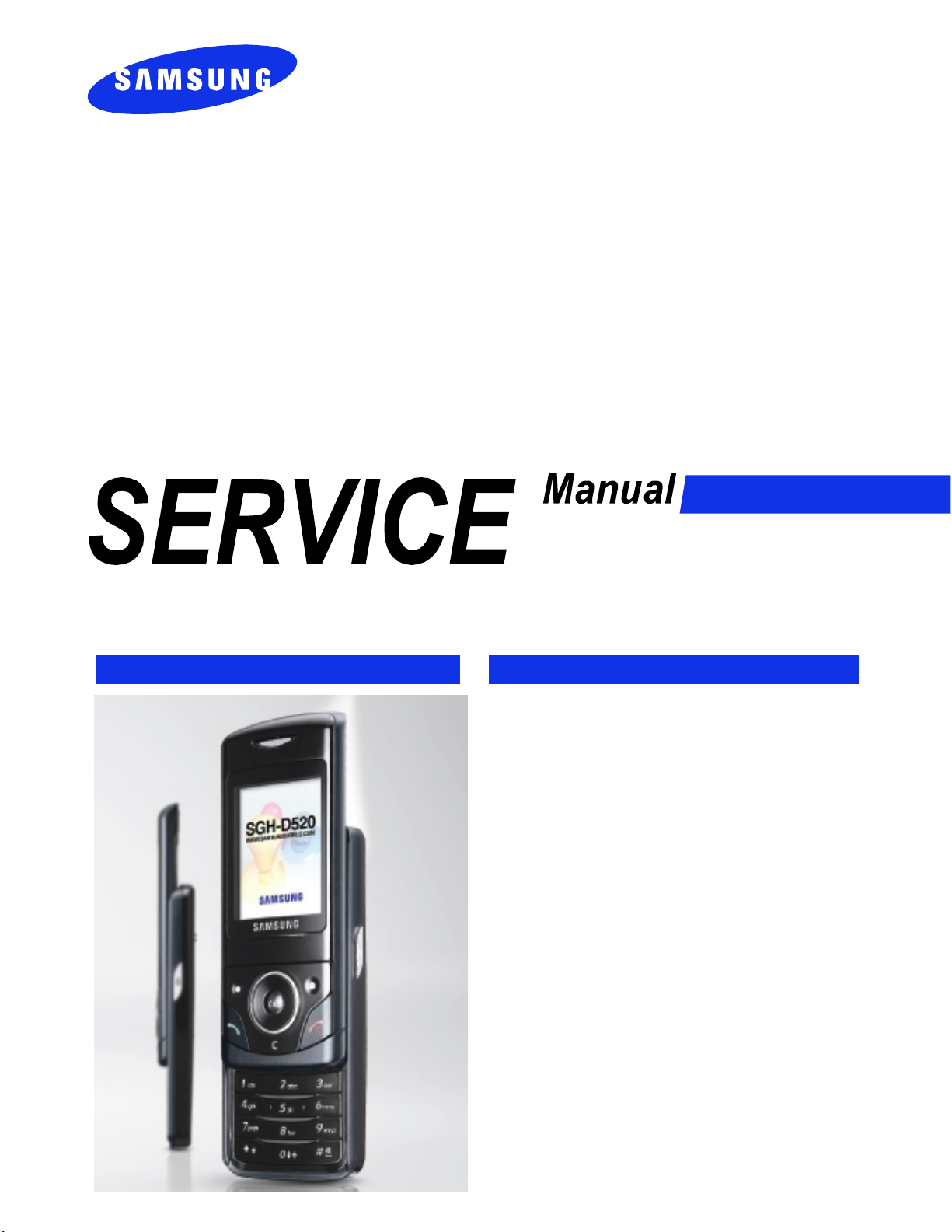
GSM TELEPHONE
SGH-D520
GSM TELEPHONE
CONTENTS
1. Safety Precautions
2. Specification
3. Product Function
4. Array course control
5. Exploded View and Parts list
6. MAIN Electrical Parts List
7. Block Diagrams
8. PCB Diagrams
9. Flow Chart of Troubleshooting
10. Reference data
11. Exploded and assembling View
This Service Manual is a property of Samsung Electronics Co.,Ltd.
Any unauthorized use of Manual can be punished under applicable
International and/or domestic law.
ⓒ
Samsung Electronics Co.,Ltd.
Code No.: GH68-10734A
2006. 04. Rev.1.0

목차
1. Safety Precautions
1-1. Repair Precaution ...........................................................................1-1
1-2. ESD(Electrostatically Sensitive Devices) Precaution ...........................1-2
2. Specification
2-1. GSM General Specification ..............................................................2-1
2-2. GSM TX power Level ......................................................................2-2
3. Product Function
4. Array course control
4-1. Downloading Binary Files .............................................................4-2
4-2. Pre-requsite for Downloading .......................................................4-2
4-3. S/W Downloader Program ...........................................................4-3
5. Exploded View and Parts list
5-1. Cellular phone Exploded View ......................................................5-1
5-2. Cellular phone Parts list ..............................................................5-2
6. MAIN Electrical Pa rts List
7. Block Diagrams
8. PCB Diagrams
9. Flow Chart of Troubleshooting
9-1. Baseband ..................................................................................9-1
9-1-1. Power ON .............................................................................9-1
9-1-2. Initial ...................................................................................9-4
9-1-3. SIM Part ...............................................................................9-6
9-1-4. Microphone Part ....................................................................9-7
9-1-5. Speaker Part_1(MP3, SPEAKER PHONE) ...................................9-8
9-1-6. Speaker Part_2(RECEIVER) ...................................................9-10
9-1-7. Charging Part ......................................................................9-11

목차
9-2. RF ..........................................................................................9-13
9-2-1. EGSM RX ............................................................................9-13
9-2-2. DCS RX ..............................................................................9-15
9-2-3. PCS RX ...............................................................................9-16
9-2-4. EGSM TX ............................................................................9-17
9-2-5. DCS TX ..............................................................................9-18
9-2-6. PCS TX ...............................................................................9-19
10. Reference data
11. Exploded and assembling View
11-1. Cellular phone Exploded View ...................................................11-1
11-2. Cellular phone assembling ........................................................11-2
11-3. Slide FPCB KIT assembling .....................................................11-29

1. Safety Precautions
1-1. Repair Precaution
●
Repair in Shield Box, during detailed tuning.
Take specially care of tuning or test,
because specipicty of cellular phone is sensitive for surrounding interference(RF noise).
●
Be careful to use a kind of magnetic object or tool,
because performance of parts is damaged by the influence of manetic force.
●
Surely use a standard screwdriver when you disassemble this product,
otherwise screw will be worn away.
●
Use a thicken twisted wire when you measure level.
A thicken twisted wire has low resistance, therefore error of measurement is few.
●
Repair after separate Test Pack and Set because for short danger (for example an
overcurrent and furious flames of parts etc) when you repair board in condition of
connecting Test Pack and tuning on.
●
Take specially care of soldering, because Land of PCB is small and weak in heat.
●
Surely tune on/off while using AC power plug, because a repair of battery charger is
dangerous when tuning ON/OFF PBA and Connector after disassembing charger.
●
Don't use as you pleases after change other material than replacement registered on SEC
System.
Otherwise engineer in charge isn't charged with problem that you don't keep this rules.
1-1
SAMSUNG Proprietary-Contents may change without notice
This Document can not be used without Samsung's authorization

Safety Precautions
1-2. ESD(Electrostatically Sensitive Devices) Precaution
Several semiconductor may be damaged easilly by static electricity. Such parts are called by
ESD(Electrostatically Sensitive Devices), for example IC,BGA chip etc. Read Precaution below.
You can prevent from ESD damage by static electricity.
●
Remove static electricity remained your body before you touch semiconductor or parts with
semiconductor. There are ways that you touch an earthed place or wear static electricity
prevention string on wrist.
●
Use earthed soldering steel when you connect or disconnect ESD.
●
Use soldering removing tool to break static electricity. , otherwise ESD will be damaged by
static electricity.
●
Don't unpack until you set up ESD on product. Because most of ESD are packed by box
and aluminum plate to have conductive power,they are prevented from static electricity.
●
You must maintain electric contact between ESD and place due to be set up until ESD is
connected completely to the proper place or a circuit board.
1-2
SAMSUNG Proprietary-Contents may change without notice
This Document can not be used without Samsung's authorization
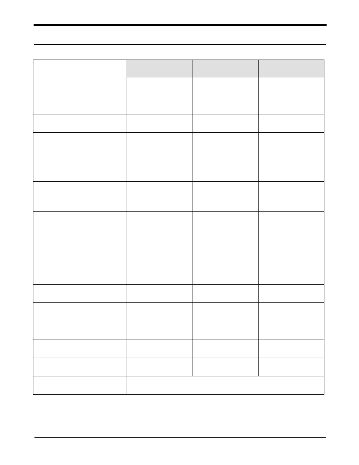
2. Specification
2-1. GSM General Specification
E-GSM DCS1800 PCS1900
Freq. Band[MHz]
Uplink/Downlink
ARFCN range
Tx/Rx spacing 45 MHz 95 M Hz 80 MHz
Mod. Bit
rate/
Bit Period
Time Slot Period/Frame
Period
Modulation GPRS 0.3 GMSK 0.3 GMSK 0.3 GMSK
MSPower GPRS 33dBm~5dBm 30dBm~0dBm 30dBm~0dBm
GPRS
880~915
925~960
975~1023
0~124
270.833 Kbps
3.692 us
576.9 us
4.615 ms
1710~1785
1805~1880
512~885 512~810
270.833 Kbps
3.692 us
576.9 us
4.615 ms
1850~1910
1930~1990
270.833 Kbps
3.692 us
576.9 us
4.615 ms
Po we r L e ve l GP RS 5~ 1 9 ( c l a s s 4 ) 0~15(class1) 0~15(class1)
Sensitivity -102 dBm -100 dBm -102 dBm
TDMAMux888
Cell Radius 35 Km 2 Km 2 Km
Operating Temperature -20℃~45
Supply Voltage 3.7 V 3.7 V 3.7 V
Size and Weight
SAMSUNG Proprietary-Contents may change without notice
This Document can not be used without Samsung's authorization
Dimention : 97(H) × 52(W) × 14.9(D) mm
Weight : 96 g (with standard battery)
℃
2-2
-20℃~45
℃
-20℃~45
℃
Specification
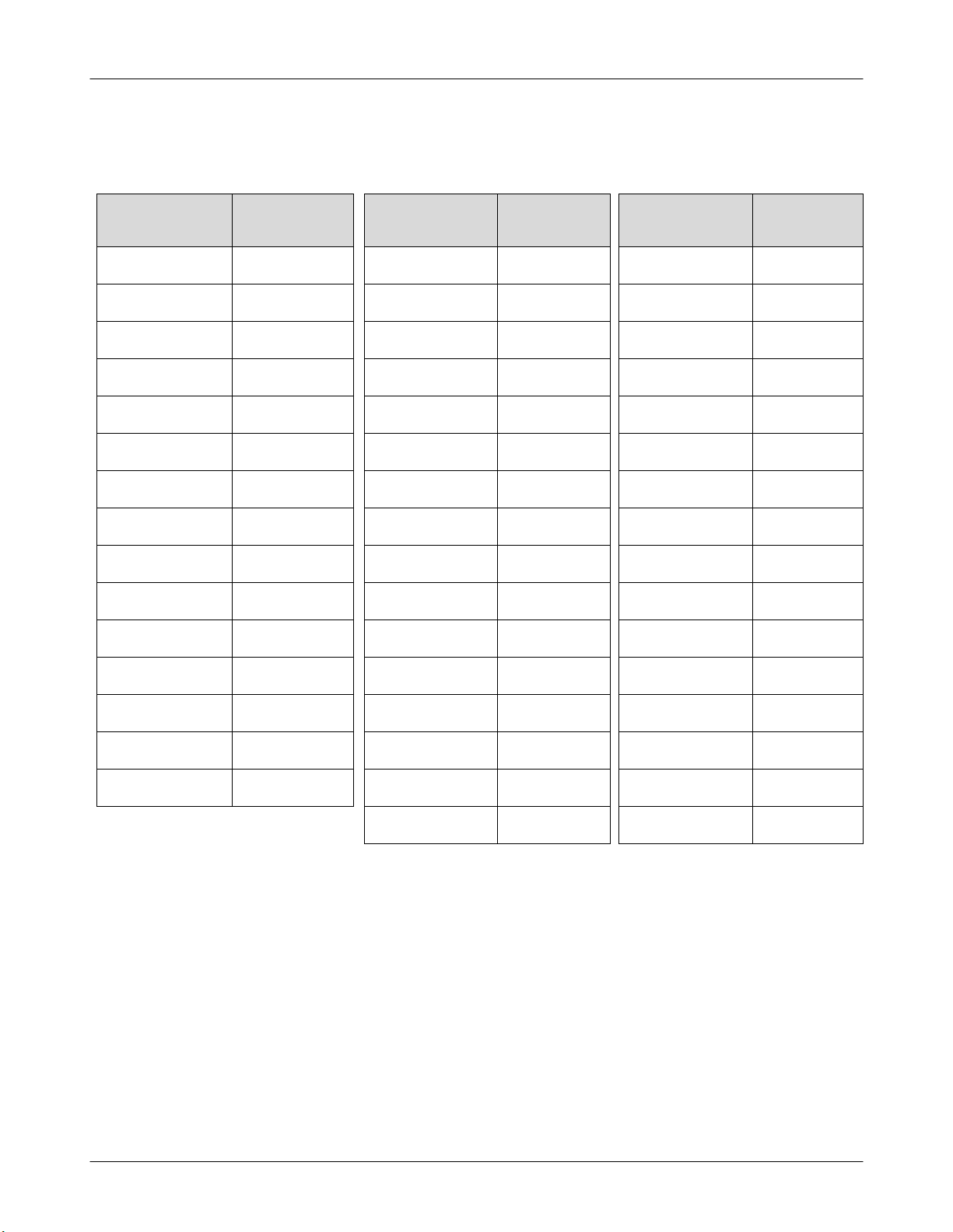
2-2. GSM TX Power Level
TX Power
control level
5 33±2 dBm
6 31±2 dBm
7 29±2 dBm
8 27±2 dBm
9 25±2 dBm
10 23±2 dBm
11 21±2 dBm
12 19±2 dBm
13 17±2 dBm
14 15±2 dBm
15 13±2 dBm
E-GSM
TX Power
control level
0 30±3 dBm
1 28±3 dBm
2 26±3 dBm
3 24±3 dBm
4 22±3 dBm
5 20±3 dBm
6 18±3 dBm
7 16±3 dBm
8 14±3 dBm
9 12±4 dBm
10 10±4 dBm
DCS1800
TX Power
control level
0 30±3 dBm
1 28±3 dBm
2 26±3 dBm
3 24±3 dBm
4 22±3 dBm
5 20±3 dBm
6 18±3 dBm
7 16±3 dBm
8 14±3 dBm
9 12±4 dBm
10 10±4 dBm
PCS1900
16 11±2 dBm
17 9±2d Bm
18 7±2d Bm
19 5±2d Bm
11 8±4 dBm
12 6±4 dBm
13 4±4 dBm
14 2±5 dBm
15 0±5 dBm
11 8±4 dBm
12 6±4 dBm
13 4±4 dBm
14 2±5 dBm
15 0±5 dBm
2-2
SAMSUNG Proprietary-Contents may change without notice
This Document can not be used without Samsung's authorization

3. Product Function
3-1. Main Function
-Camera and camcorder
-Image editor
-File viewer
-Bluetooth
-Get personal with photo caller ID
-Name card
-Multimedia Message Service (MMS)
-Email
-Web browser
-Java
-Voice recorder
3-1
SAMSUNG Proprietary-Contents may change without notice
This Document can not be used without Samsung's authorization
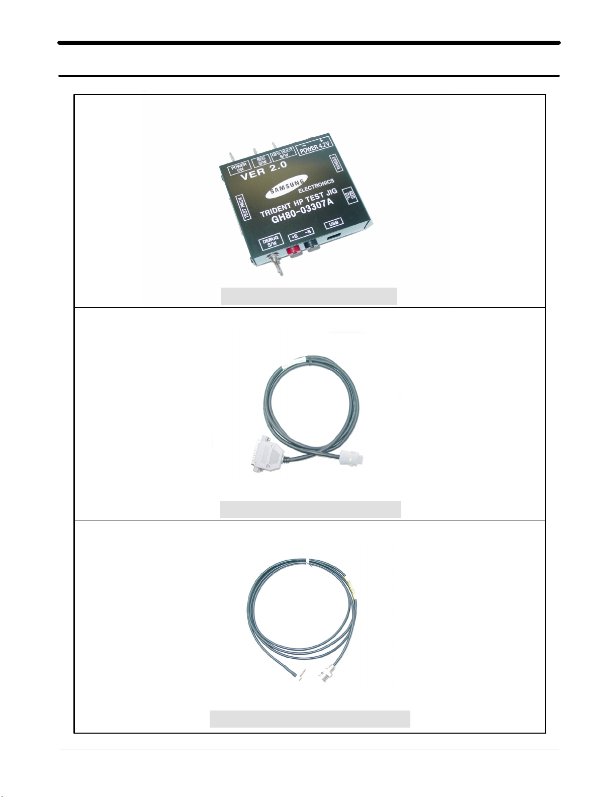
4. Array course control
Test Jig (GH80-03307A)
Test Cable (GH39-00127A)
RF Test Cable (GH39-00283A)
4-1
SAMSUNG Proprietary-Contents may change without notice
This Document can not be used without Samsung's authorization

Array course control
Software Downloading
4-1. Downloading Binary Files
• Two binary files for downloading D520.
– D520XXYY.s3 : Main source code binary.
– D520XXYY.cts : Default Contents binary.
4-2. Pre-requsite for Downloading
• Downloader Program(OptiFlash.exe)
• D520 Mobile Phone
• Data C able
• Binary files
• CTS files
4-2
SAMSUNG Proprietary-Contents may change without notice
This Document can not be used without Samsung's authorization
1.
Array course control
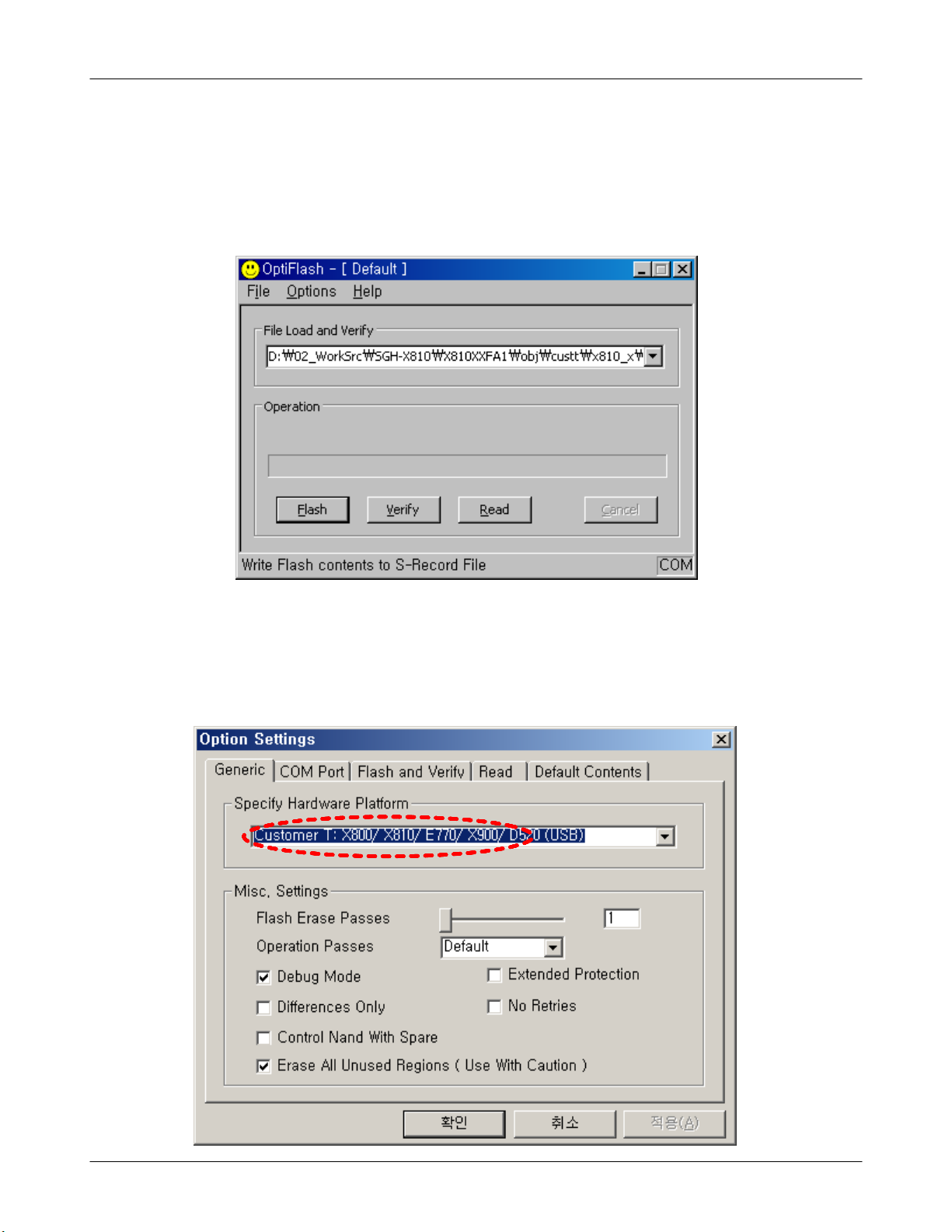
4-3. S/W Downloader Program
1. Load the binary download programby executing the “OptiFlash.exe”
2. Select the “Options” -> “Settings” -> “Generic” -> “Specify hardware
platform”.
Choose hardware platform for the downloader file setting.
Set the everything else as the default values which are shown below
4-3
SAMSUNG Proprietary-Contents may change without notice
This Document can not be used without Samsung's authorization
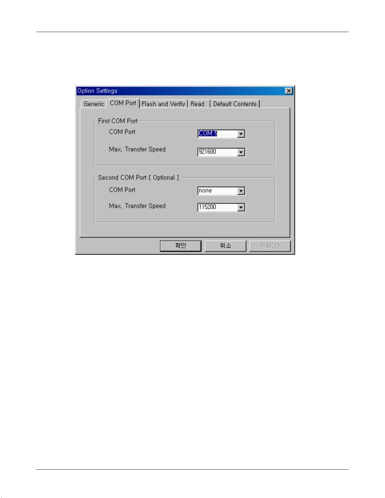
Array course control
3. Select the COM port when the download cable is connected
Up to 64 ports are supported. Additionally you can select the
maximum transfer speed OptiFlash will use to communicate with
the phone. However, OptiFlash will use a slower speed if either the
PC’s or the phone’s serial hardware is incapable of handling the
selected speed
4-4
SAMSUNG Proprietary-Contents may change without notice
This Document can not be used without Samsung's authorization
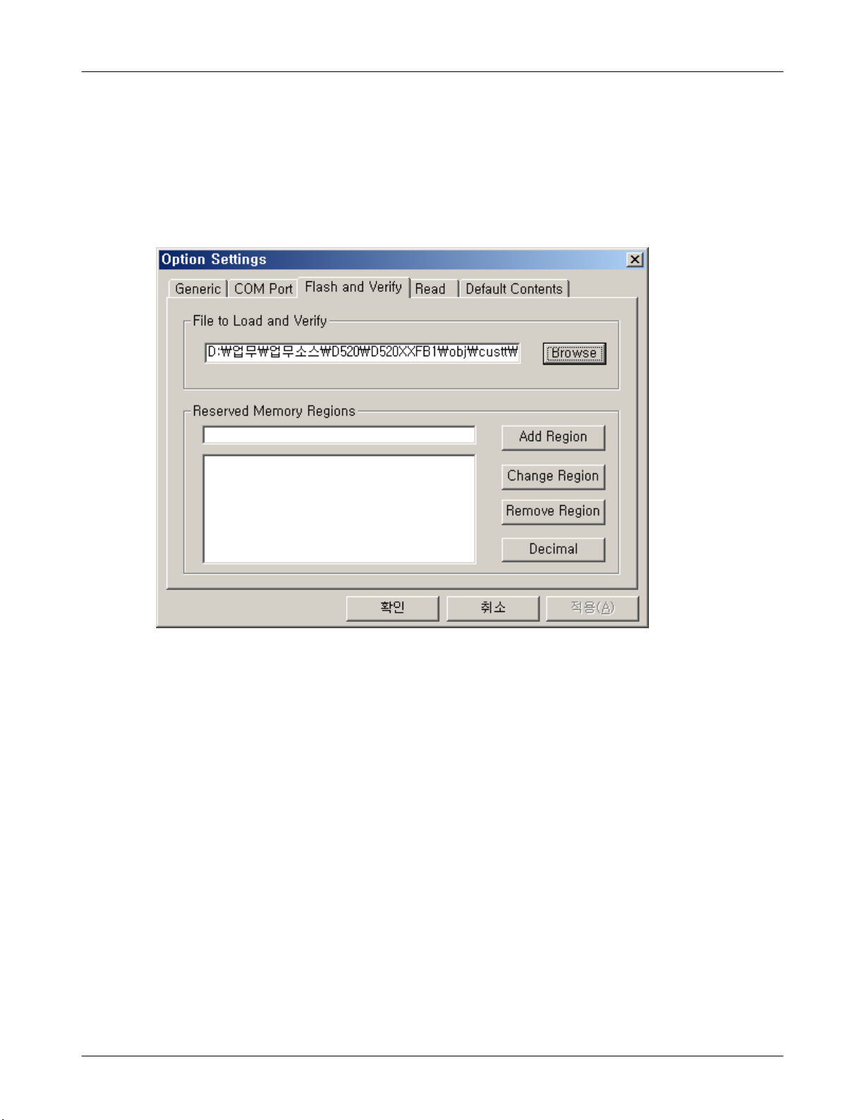
Array course control
4. Select the“Flash&Verify” -> “Browse”
Set the directory path and choose the latest s/w binary, for example
“D520XXYY.s3”,for the downloader binary setting.
In case of D520 the reserved regions are not a
necessity. (It is defined in platform.def file)
4-5
SAMSUNG Proprietary-Contents may change without notice
This Document can not be used without Samsung's authorization
Array course control
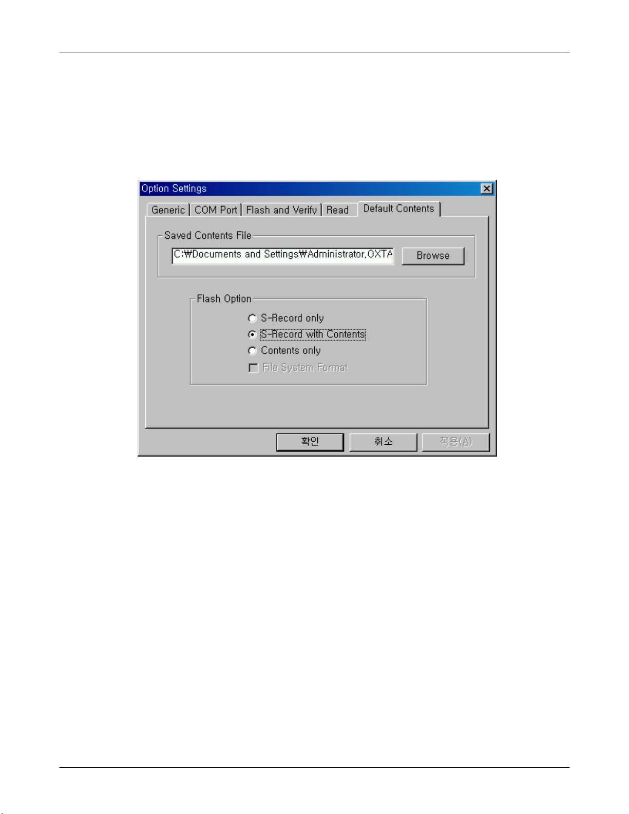
5. Select the“Default Contents” -> “Browse”
Set the directory path and choose the CTS file, for example
“D520XXYY.cts”,for the downloader binary setting.
Function of Flash option
S-Record only : download binary only
S-Record with Contens : download binary with default contents
Contents only : download default contents
4-6
SAMSUNG Proprietary-Contents may change without notice
This Document can not be used without Samsung's authorization
Array course control
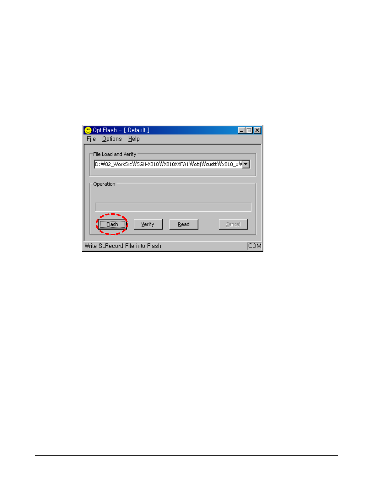
6. Click “OK” button then press “Flash”.
(Before pressing ‘Flash’ button, push the button ‘*’and ‘END’ at the same
time. Then press ‘Flash’.)
Downloader will upload the binary file as below for the downloading.
7. When downloading is finished successfully, there is a “All is well”
message.
8. After finishing downloading, Certain memory resets should b e done to
guarantee the normal performance.
9. Confirm the downloaded version name and etc. :
*#5002*8376263#
Full Reset :
*2767*3855#
4-7
SAMSUNG Proprietary-Contents may change without notice
This Document can not be used without Samsung's authorization
5. Exploded Vi ew and Par ts Li st
5- 1. Ce l l ular phone Expl oded V i ew
QFR04
QFU01
QKP01
QME01
QFR01
QCR32
QVO01
QCA02
QPC01
QVK01
QCR05
QMP01
QSH01
QRE01
QCK01
QAN02
QCA01
QMO01
QCR47
QCA05
QMI03
QSP01
QKP02
QLC01
QME02
QCR32
QHI01
QFL02
QFL01
QCR12
QIF01
QBA01
QBA00
QRF01
5-1
SAMSUNG Proprietary-Contents may change without notice
This Doc umen t can n ot be use d withou t S a m su n g's authoriza tion
Ma in Ele ctrica l Par ts List
5- 2. Ce l l ular phone Par t s list
De sig n LO C D iscrip tion SE C C O D E
QA N 0 2
QB A 0 0
QB A 0 1
QC A 0 1
QC A 0 2
QC A 0 5
QC K 0 1
QC R 0 5
QC R 0 5
QC R 1 2
QC R 3 2
QF R 01
QF R 04
QK P 01
QK P 02
QL C 01
QME 0 1
QME 0 2
QM O0 1
QM P 0 1
QP C 0 1
QR F 01
QS H 0 1
QS P 01
QV K 0 1
QV O 0 1
QR E 0 1
ㅤ
QF L0 1
ㅤ
ㅤ
ㅤ
ㅤ
QF U 0 1
ㅤ
ㅤ
ㅤ
ㅤ
ㅤ
ㅤ
ㅤ
ㅤ
ㅤ
ㅤ
ㅤ
ㅤ
ㅤ
ㅤ
ㅤ
ㅤ
ㅤ
ㅤ
ㅤ
ㅤ
ㅤ
ㅤ
ㅤ
ㅤ
ㅤ
ㅤ
ㅤ
ㅤ
QIF 01 PM O -I F COV E R GH 7 2 -2 78 5 8B
ㅤ
QC R 3 2 SC R EW- M A C H IN E 600 1 -0 01 7 00
QC R 4 7 SC R EW- M A C H IN E 600 1 -0 01 6 95
QF L0 2 MEC -S L ID E LOWE R GH 7 5- 08 8 60 B
QH I0 1 M E C -H IN G E GH 7 5 -0 94 1 4A
ㅤ
QMI0 3 RM O -MIC HO L D E R GH 7 3 -0 57 0 4A
INN E R B A T TE R Y P AC K - 80 0MA H ,B LK , GH 4 3 -0 18 5 0A
INT ENN A -S G H D 5 2 0 GH 4 2 -0 07 4 0A
AS S Y- COV E R- B AT T GH 9 8 -0 07 2 1B
UN IT -C A ME RA GH 5 9 -0 28 6 0A
UN IT -C A M E R A K E Y GH 59 -0 2 7 99 A
ME C -S U B F LA S H D E C O GH 7 5 -0 88 6 2A
ME C -C A M KE Y GH 7 5 -0 88 6 6A
SC R EW- M A C H IN E 600 1 -0 01 4 78
SC R EW- M A C H IN E 600 1 -0 01 4 78
SC R EW- M A C H IN E 600 1 -0 01 5 30
SC R EW- M A C H IN E 600 1 -0 01 7 00
ME C -S U A F R O N T C O V E R GH 7 5 -0 88 6 3B
PM O -F R O N T C O V E R B U SH GH 7 2 -2 78 5 6A
ME C -K E Y PA D MAIN GH 7 5 -0 88 6 4B
M EC -K E Y PA D SU B GH 7 5 -0 88 6 1B
ELA U NIT -S G H D 5 2 0 LC D GH 96 -0 2 0 99 A
UN IT -K E Y P A D GH 5 9 -0 27 1 6A
UN IT -N A V I K EY GH 5 9 -0 27 1 7A
MO T O R DC -S P H V 8 40 0 GH 3 1 -0 01 8 7A
PBA MA IN - S G H D 5 20 GH 9 2 -0 24 8 1A
ME A -S LI D E FP C B K IT GH 9 7 -0 55 7 9A
PM O -CO V E R R F GH 72 -2 9 40 5 B
ND C -S H IE L D C A N GH 7 1- 05 9 61 A
SP E AK E R 300 1 -0 01 9 06
UN IT -V O L U M E K E Y GH 5 9 -0 27 98 A
ME C -K E Y V O LU ME GH7 5 -0 82 7 7 A
M EC -S U A R E A R C O V E R GH75 - 08 8 65 B
M EC -S U A S L ID E L O W HIN G E GH 7 5 -0 88 5 9B
M EC -S U A S L ID E U P PE R GH 7 5 -0 88 5 7B
5-2
SAMSUNG Proprietary-Contents may change without notice
This Doc umen t can n ot be use d withou t S a m su n g's authoriza tion
Ma in Ele ctrica l Par ts List
Disc rip tion SE C C O D E
BA G P E 690 2 -00 0 2 97
CB F IN TE R F AC E -D A T A L IN K C A B LE G H 3 9- 00 4 44 A
AD A P TO R -S GH D 8 00 T A (E U ) GH 4 4 -01 0 6 0A
S/W C D -S AMSU N G P CST U D IO 3 .0 GH4 6- 00 2 15 A
EA R PH O N E - ST E R EO HE A D S E T G H 5 9 -02 4 99 A
LAB E L( P) -IM E I GH 6 8- 01 3 35 D
LAB E L( P) -W A T E R S O A K GH 6 8 -02 0 2 6A
LAB E L( P) -W A T E R S O A K GH 6 8 -02 0 2 6A
MA N U A L -S FC CA R D GH 6 8 -07 9 3 7A
MA N U A L U S E RS -E U F R E N C H GH 6 8 -09 2 0 5A
LAB E L( P) -M A IN (EU ) GH 6 8 -09 2 5 1A
MA N U A L U S E RS -E U DU T C H GH 6 8 -09 5 0 9A
CU S H IO N -CA S E TA 2 MA 2 GH 6 9 -03 6 3 2A
BO X (P )-U N I T M A IN (E U ) GH 6 9 -03 6 3 5A
MP R -B O H O VIN Y L LC D CO N N GH 7 4 -15 3 5 0A
MP R -T A PE R E M OV E LC D GH 7 4 -18 2 8 6A
MP R -V IN Y L B O H O M A I N GH7 4 -19 9 51 A
MP R -T A PE GA S KE T MA IN FPC GH 7 4 -21 3 6 1A
MP R -T A PE N A V I C O N N B T M GH7 4- 21 36 2 A
MP R -T A PE CA M E R A C O N N GH 7 4 -21 3 6 4A
MP R -T A PE L C D C O N N C GH 7 4- 21 3 65 A
M PR -T A PE N AV I KE Y C O N N GH 7 4 -21 3 6 6A
MP R -T A PE MA IN CO N N C GH 7 4 -21 3 67 A
M PR -T A PE MA I N C O N N A G H7 4 -21 3 68 A
MP R -T A PE L C D C O N N D GH7 4 -21 3 6 9A
M PR -C U S H IO N NA V I KE Y GH 7 4 -21 6 2 6A
MP R -C U S H IO N LC D B A CK GH 74 -2 16 2 7A
MP R -V IN Y L B O H O S U B K E Y G H 7 4 -22 2 2 5A
5-3
SAMSUNG Proprietary-Contents may change without notice
This Doc umen t can n ot be use d withou t S a m su n g's authoriza tion

6. MAIN Electrical Parts List
SEC CODE Design LOC Discription STATUS
4202-001095 ANT602 ANTENNA-CHIP SA
4302-001201 BAT100 BATTERY-LI(2ND) SA
3711-006025 BTC502 HEADER-BATTERY SA
2203-006194 C100 C-CER,CHIP SA
2203-006194 C101 C-CER,CHIP SA
2203-006423 C102 C-CER,CHIP SA
2203-006423 C103 C-CER,CHIP SA
2203-006324 C104 C-CER,CHIP SA
2203-006562 C105 C-CER,CHIP SA
2203-006562 C106 C-CER,CHIP SA
2203-006562 C107 C-CER,CHIP SA
2203-006562 C108 C-CER,CHIP SA
2203-006562 C109 C-CER,CHIP SA
2203-006562 C110 C-CER,CHIP SA
2203-006562 C111 C-CER,CHIP SA
2203-005736 C112 C-CER,CHIP SA
2203-006648 C113 C-CER,CHIP SA
2203-006194 C114 C-CER,CHIP SA
2203-001405 C115 C-CER,CHIP SA
2203-006562 C116 C-CER,CHIP SA
2203-006423 C117 C-CER,CHIP SA
2203-006121 C118 C-CER,CHIP SA
2203-006423 C119 C-CER,CHIP SA
2203-005682 C120 C-CER,CHIP SA
2203-005682 C121 C-CER,CHIP SA
2203-005729 C122 C-CER,CHIP SA
2203-006257 C124 C-CER,CHIP SA
2203-006562 C125 C-CER,CHIP SA
2203-006423 C126 C-CER,CHIP SA
2203-006562 C128 C-CER,CHIP SA
2203-006562 C129 C-CER,CHIP SA
2203-006825 C130 C-CER,CHIP SA
2203-006562 C131 C-CER,CHIP SA
2203-006825 C132 C-CER,CHIP SA
2203-006562 C135 C-CER,CHIP SA
2203-006423 C136 C-CER,CHIP SA
2203-006348 C137 C-CER,CHIP SA
2203-006324 C138 C-CER,CHIP SA
2203-006194 C200 C-CER,CHIP SA
2203-006194 C201 C-CER,CHIP SA
2203-006423 C202 C-CER,CHIP SA
2203-006423 C203 C-CER,CHIP SA
6-1
SAMSUNG Proprietary-Contents may change without notice
This Document can not be used without Samsung's authorization

Main Electrical Parts List
SEC CODE Design LOC Discription STATUS
2203-006423 C204 C-CER,CHIP SA
2203-006194 C205 C-CER,CHIP SA
2203-006423 C206 C-CER,CHIP SA
2203-006194 C207 C-CER,CHIP SA
2203-006423 C208 C-CER,CHIP SA
2203-005727 C209 C-CER,CHIP SA
2203-005727 C210 C-CER,CHIP SA
2203-000254 C211 C-CER,CHIP SA
2203-005806 C212 C-CER,CHIP SA
2203-005806 C213 C-CER,CHIP SA
2203-006423 C215 C-CER,CHIP SA
2203-006194 C216 C-CER,CHIP SA
2203-006194 C217 C-CER,CHIP SA
2203-006423 C218 C-CER,CHIP SA
2203-006562 C300 C-CER,CHIP SA
2203-006562 C301 C-CER,CHIP SA
2203-006423 C302 C-CER,CHIP SA
2203-006562 C303 C-CER,CHIP SA
2203-006423 C304 C-CER,CHIP SA
2203-006305 C305 C-CER,CHIP SA
2203-006305 C306 C-CER,CHIP SA
2203-006562 C309 C-CER,CHIP SA
2203-006423 C312 C-CER,CHIP SA
2203-006324 C313 C-CER,CHIP SA
2203-006423 C314 C-CER,CHIP SA
2203-006379 C315 C-CER,CHIP SA
2203-006423 C316 C-CER,CHIP SA
2203-006562 C317 C-CER,CHIP SA
2203-006648 C318 C-CER,CHIP SA
2203-005806 C319 C-CER,CHIP SA
2203-006423 C320 C-CER,CHIP SA
2203-000654 C321 C-CER,CHIP SA
2203-006423 C322 C-CER,CHIP SA
2203-006423 C326 C-CER,CHIP SA
2203-006423 C327 C-CER,CHIP SA
2203-002709 C328 C-CER,CHIP SA
2203-006423 C330 C-CER,CHIP SA
2203-006423 C331 C-CER,CHIP SA
2203-006668 C332 C-CER,CHIP SA
2203-006423 C333 C-CER,CHIP SA
2203-006423 C342 C-CER,CHIP SA
2203-006562 C343 C-CER,CHIP SA
6-2
SAMSUNG Proprietary-Contents may change without notice
This Document can not be used without Samsung's authorization

Main Electrical Parts List
SEC CODE Design LOC Discription STATUS
2203-006562 C344 C-CER,CHIP SA
2203-006260 C347 C-CER,CHIP SA
2203-006260 C348 C-CER,CHIP SA
2203-006348 C400 C-CER,CHIP SA
2203-006423 C401 C-CER,CHIP SA
2203-000854 C403 C-CER,CHIP SA
2203-000854 C404 C-CER,CHIP SA
2203-006562 C406 C-CER,CHIP SA
2203-006423 C407 C-CER,CHIP SA
2203-005682 C408 C-CER,CHIP SA
2203-005682 C409 C-CER,CHIP SA
2203-005682 C410 C-CER,CHIP SA
2203-005682 C411 C-CER,CHIP SA
2203-006257 C413 C-CER,CHIP SA
2203-005682 C414 C-CER,CHIP SA
2203-006626 C415 C-CER,CHIP SA
2203-005682 C416 C-CER,CHIP SA
2203-005683 C417 C-CER,CHIP SA
2203-006348 C418 C-CER,CHIP SA
2203-005682 C419 C-CER,CHIP SA
2203-006626 C420 C-CER,CHIP SA
2203-005682 C421 C-CER,CHIP SA
2203-006348 C422 C-CER,CHIP SA
2203-005682 C423 C-CER,CHIP SA
2203-006260 C424 C-CER,CHIP SA
2203-006260 C426 C-CER,CHIP SA
2203-005682 C429 C-CER,CHIP SA
2203-006825 C432 C-CER,CHIP SA
2203-006825 C433 C-CER,CHIP SA
2203-005736 C500 C-CER,CHIP SA
2203-006048 C502 C-CER,CHIP SA
2203-006562 C503 C-CER,CHIP SA
2203-006257 C505 C-CER,CHIP SA
2007-008055 C506 R-CHIP SA
2203-005682 C507 C-CER,CHIP SA
2203-006423 C508 C-CER,CHIP SA
2203-006423 C509 C-CER,CHIP SA
2203-006423 C510 C-CER,CHIP SA
2203-006423 C511 C-CER,CHIP SA
2203-005736 C512 C-CER,CHIP SA
2203-005736 C513 C-CER,CHIP SA
2203-006648 C542 C-CER,CHIP SA
6-3
SAMSUNG Proprietary-Contents may change without notice
This Document can not be used without Samsung's authorization

Main Electrical Parts List
SEC CODE Design LOC Discription STATUS
2203-006194 C543 C-CER,CHIP SA
2203-005682 C600 C-CER,CHIP SA
2203-005736 C601 C-CER,CHIP SA
2203-006194 C602 C-CER,CHIP SA
2203-005806 C603 C-CER,CHIP SA
2203-006556 C604 C-CER,CHIP SA
2203-005682 C605 C-CER,CHIP SA
2203-006423 C606 C-CER,CHIP SA
2203-006648 C607 C-CER,CHIP SA
2203-006423 C608 C-CER,CHIP SA
2203-006194 C609 C-CER,CHIP SA
2203-005792 C610 C-CER,CHIP SA
2203-005792 C611 C-CER,CHIP SA
2203-006318 C612 C-CER,CHIP SA
2203-006318 C613 C-CER,CHIP SA
2203-006318 C614 C-CER,CHIP SA
2203-006318 C615 C-CER,CHIP SA
2203-005736 C616 C-CER,CHIP SA
2203-005736 C617 C-CER,CHIP SA
2203-005736 C618 C-CER,CHIP SA
2203-006556 C619 C-CER,CHIP SA
2203-006318 C620 C-CER,CHIP SA
2203-006423 C622 C-CER,CHIP SA
2203-006194 C623 C-CER,CHIP SA
2203-006423 C625 C-CER,CHIP SA
2203-005682 C626 C-CER,CHIP SA
2203-006620 C627 C-CER,CHIP SNA
2203-005682 C628 C-CER,CHIP SA
2203-005682 C629 C-CER,CHIP SA
2203-005682 C630 C-CER,CHIP SA
2203-006194 C631 C-CER,CHIP SA
2203-006423 C632 C-CER,CHIP SA
2203-006324 C633 C-CER,CHIP SA
2203-005682 C635 C-CER,CHIP SA
2203-005682 C636 C-CER,CHIP SA
2203-006324 C637 C-CER,CHIP SA
2203-006305 C638 C-CER,CHIP SA
2203-005725 C639 C-CER,CHIP SA
2203-006562 C640 C-CER,CHIP SA
2203-006562 C641 C-CER,CHIP SA
2203-005158 C642 C-CER,CHIP SA
2901-001256 F101 FILTER-EMI SMD SA
6-4
SAMSUNG Proprietary-Contents may change without notice
This Document can not be used without Samsung's authorization

Main Electrical Parts List
SEC CODE Design LOC Discription STATUS
2901-001337 F500 FILTER-EMI/ESD SA
2901-001337 F501 FILTER-EMI/ESD SA
2901-001337 F502 FILTER-EMI/ESD SA
2901-001337 F503 FILTER-EMI/ESD SA
2901-001337 F504 FILTER-EMI/ESD SA
2901-001337 F505 FILTER-EMI/ESD SA
2901-001337 F506 FILTER-EMI/ESD SA
2904-001592 F600 FILTER-SAW SA
2904-001599 F601 FILTER-SAW SA
2904-001601 F602 FILTER-SAW SA
3711-006109 HDC500 HEADER-BOARD TO BOARD SNA
3710-002306 IFC503 SOCKET-INTERFACE SA
2703-002749 L100 INDUCTOR-SMD SA
2703-002734 L101 INDUCTOR-SMD SA
2007-000171 L300 R-CHIP SA
2007-000171 L301 R-CHIP SA
3301-001729 L302 BEAD-SMD SA
2703-002485 L600 INDUCTOR-SMD SA
2703-002544 L601 INDUCTOR-SMD SA
2703-002608 L602 INDUCTOR-SMD SA
2703-002917 L603 INDUCTOR-SMD SA
2703-002917 L604 INDUCTOR-SMD SA
2703-002558 L605 INDUCTOR-SMD SA
2703-002313 L607 INDUCTOR-SMD SA
2801-004466 OSC200 CRYSTAL-SMD SA
2801-004225 OSC300 CRYSTAL-SMD SA
2801-004455 OSC600 CRYSTAL-SMD SA
2801-004426 OSC601 CRYSTAL-SMD SA
1201-002278 PAM601 IC-POWER AMP SA
0504-000168 Q100 TR-DIGITAL SA
2007-008588 R100 R-CHIP SA
2007-009166 R101 R-CHIP SA
2007-008419 R102 R-CHIP SA
2007-008055 R103 R-CHIP SA
2007-000142 R104 R-CHIP SA
2007-008483 R105 R-CHIP SA
2007-008052 R106 R-CHIP SA
2007-009167 R107 R-CHIP SA
2007-008516 R108 R-CHIP SA
2007-008483 R109 R-CHIP SA
2007-008478 R110 R-CHIP SA
2007-009115 R111 R-CHIP SA
6-5
SAMSUNG Proprietary-Contents may change without notice
This Document can not be used without Samsung's authorization
Main Electrical Parts List
SEC CODE Design LOC Discription STATUS
2007-009115 R112 R-CHIP SA
2007-009212 R115 R-CHIP SA
2007-000172 R201 R-CHIP SA
2007-008531 R202 R-CHIP SA
2007-008806 R203 R-CHIP SA
2007-000162 R204 R-CHIP SA
2007-008055 R205 R-CHIP SA
2007-008483 R206 R-CHIP SA
2007-008531 R207 R-CHIP SA
2007-008055 R208 R-CHIP SA
2007-000171 R210 R-CHIP SA
2007-009084 R300 R-CHIP SA
2007-000157 R301 R-CHIP SA
2007-000171 R302 R-CHIP SA
2007-008542 R304 R-CHIP SA
2007-008531 R308 R-CHIP SA
2007-008483 R309 R-CHIP SA
2007-008516 R312 R-CHIP SA
2007-008483 R313 R-CHIP SA
2007-008051 R314 R-CHIP SA
2007-009166 R315 R-CHIP SA
2007-008055 R316 R-CHIP SA
2007-009166 R317 R-CHIP SA
2007-000138 R319 R-CHIP SA
2007-009084 R320 R-CHIP SA
2007-009169 R321 R-CHIP SA
2007-009169 R322 R-CHIP SA
2007-007310 R323 R-CHIP SA
2007-008210 R326 R-CHIP SA
2007-008210 R327 R-CHIP SA
2203-006091 R328 C-CER,CHIP SA
2203-006091 R329 C-CER,CHIP SA
2007-009084 R330 R-CHIP SA
2007-009084 R331 R-CHIP SA
2007-000171 R400 R-CHIP SA
2007-001292 R403 R-CHIP SA
2007-001292 R406 R-CHIP SA
2007-008420 R409 R-CHIP SA
2007-008420 R410 R-CHIP SA
2007-001119 R411 R-CHIP SA
2007-007528 R412 R-CHIP SA
2007-007528 R413 R-CHIP SA
6-6
SAMSUNG Proprietary-Contents may change without notice
This Document can not be used without Samsung's authorization