

Samsung SGH-D500 Service Manual
GPRS TELEPHONE
SGH-D500
GPRS TELEPHONE
CONTENTS
1. Specification
2. Circuit Description
3. Exploded Views and Parts List
4. Electrical Parts List
5. Block Diagrams
6. PCB Diagrams
7. Flow Chart of Troubleshooting
This Service Manual is a property of Samsung Electronics Co.,Ltd.
Any unauthorized use of Manual can be punished under applicable
International and/or domestic law.
ⓒ
Samsung Electronics Co.,Ltd. Nov. 2004
Printed in South Korea.
Code No.:
BASIC.
GH68-05955A
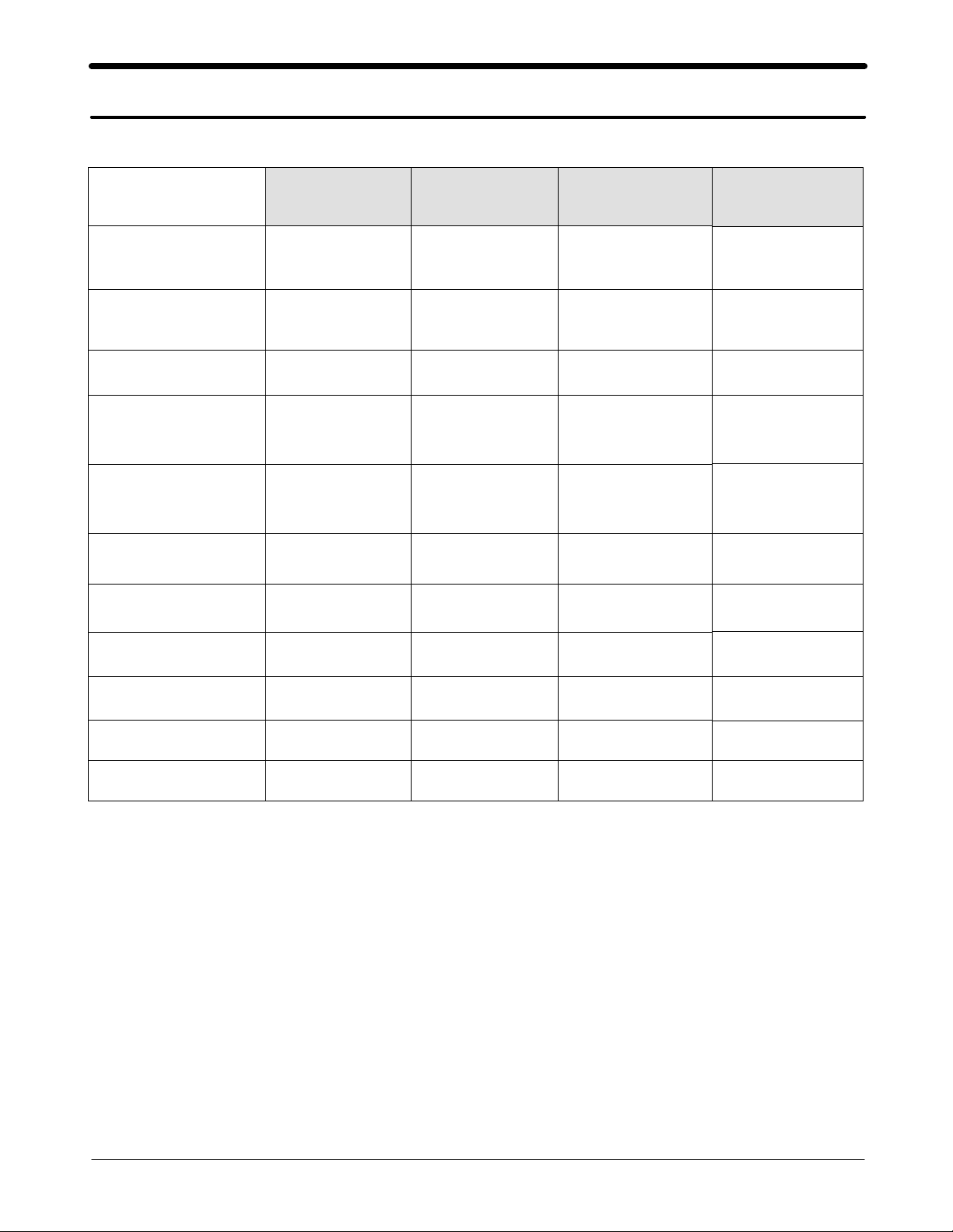
1. SGH-D500 Specification
1. GSM General Specification
GSM900
Phase 1
Freq. Band[MHz]
Uplink/Downlink
ARFCN range 1~124
Tx/Rx spacing 45MHz 45MHz 95MHz
Mod. Bit rate
/ Bit Period
Time Slot Period
/ Frame Period
Modulation 0.3GMSK 0.3GMSK 0.3GMSK
MS Power 33dBm~5dBm 33dBm~5dBm 30dBm~0dBm
890~915
935~960
270.833kbps
3.692us
576.9us
4.615ms
EGSM 900
Phase 2
880~915
925~960
0~124 &
975~1023
270.833kbps
3.692us
576.9us
4.615ms
DCS1800
Phase 1
1710~1785
1805~1880
512~885
270.833kbps
3.692us
576.9us
4.615ms
PCS1900
1850~1910
1930~1990
512~810
80MHz
270.833kbps
3.692us
576.9us
4.615ms
0.3GMSK
30dBm~0dBm
Power Class 5pcl ~ 19pcl 5pcl ~ 19pcl 0pcl ~ 15pcl
Sensitivity -102dBm -102dBm -100dBm
TDMA Mux 8 8 8
Cell Radius 35Km 35Km 2Km
0pcl ~ 15pcl
-100dBm
8
-
1-1
SAMSUNG Proprietary-Contents may change without notice
This Document can not be used without Samsung's authorization
Specification
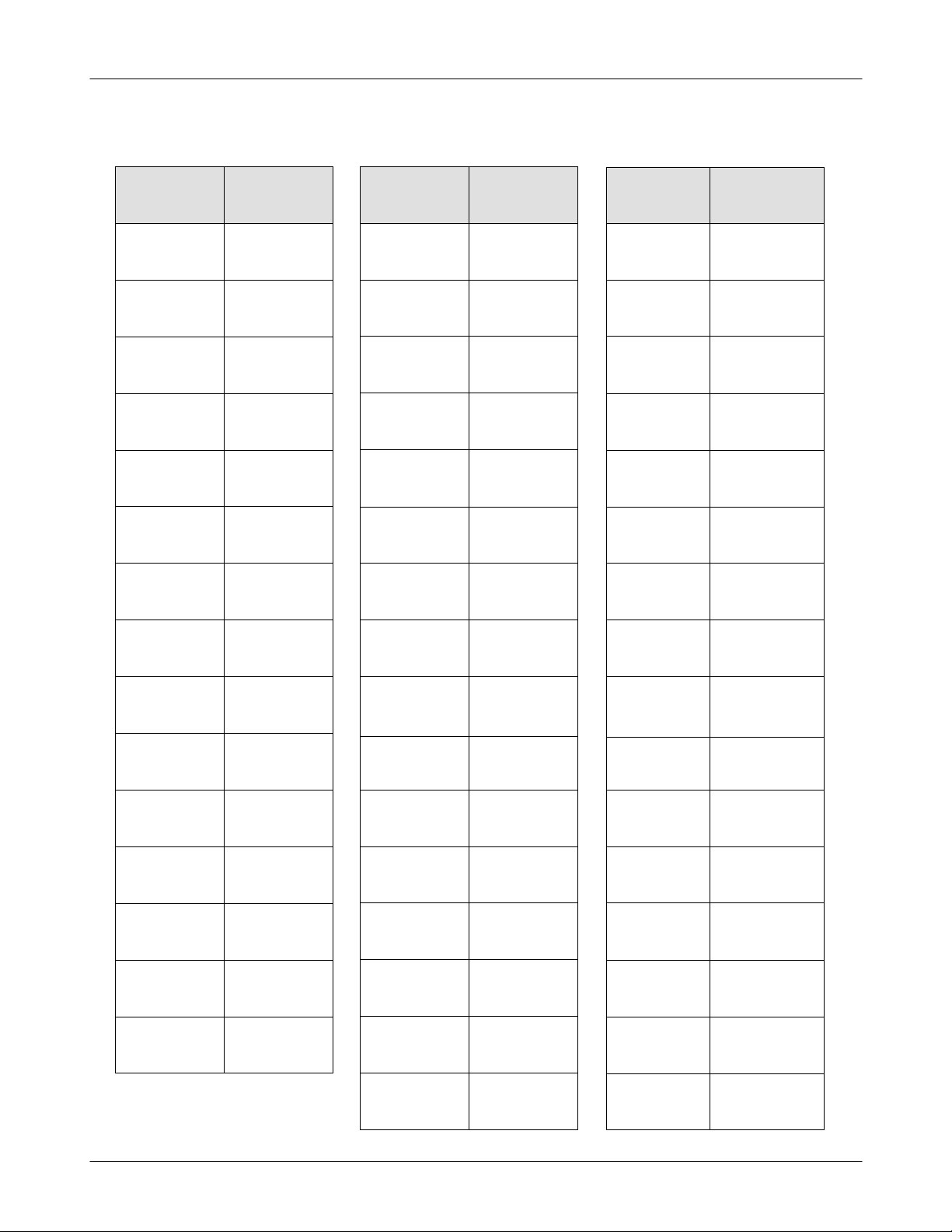
2. GSM TX power class
TX Power
control level
5 33±3 dBm
6 31±3 dBm
7 29±3 dBm
8 27±3 dBm
9 25±3 dBm
10 23±3 dBm
11 21±3 dBm
GSM900
TX Power
control level
0 30±3 dBm
1 28±3 dBm
2 26±3 dBm
3 24±3 dBm
4 22±3 dBm
5 20±3 dBm
6 18±3 dBm
DCS1800
TX Power
control level
0 30±3 dBm
1 28±3 dBm
2 26±3 dBm
3 24±3 dBm
4 22±3 dBm
5 20±3 dBm
6 18±3 dBm
PCS1900
12 19±3 dBm
13 17±3 dBm
14 15±3 dBm
15 13±3 dBm
16 11±5 dBm
17 9±5 dBm
18 7±5 dBm
19 5±5 dBm
7 16±3 dBm
8 14±3 dBm
9 12±4 dBm
10 10±4 dBm
11 8±4dBm
12 6±4 dBm
13 4±4 dBm
14 2±5 dBm
7 16±3 dBm
8 14±3 dBm
9 12±4 dBm
10 10±4 dBm
11 8±4dBm
12 6±4 dBm
13 4±4 dBm
14 2±5 dBm
15 0±5 dBm
1-2
15 0±5 dBm
SAMSUNG Proprietary-Contents may change without notice
This Document can not be used without Samsung's authorization
2. SGH-D500 Circuit Description
1. SGH-D500 RF Circuit Description
1) RX PART
1. ANTENNA SWITCH (U100 SWICHPLEXER)
→
Switching Tx, Rx path for GSM900, DCS1800 and PCS1900 by logic controlling.
2. ANTENNA SWITCH Control Losic (U100)→Truth Table
VC1 VC2 VC3
Tx Mode (GSM900) L H L
Tx Mode (DCS1800/1900) L(H) L H
Rx Mode (GSM900) L L L
Rx Mode (DCS1800) L L L
Rx Mode (PCS1900) H L L
3. FILTER
To convert Electromagnetic Field Wave to Acoustic Wave and then pass the specific frequency band.
- GSM FILTER (F100)→For filtering the frequency band between 925 and 960 MHz
- DCS FILTER (F102)→For filtering the frequency band between 1805 and 1880 MHz.
- PCS FILTER (F101)→For filtering the frequency band between 1930 and 1990 MHz.
4. VC-TCXO (U101)
This module generates the 26MHz reference clock to drive the logic and RF.
It is turned on when the supply voltage Vcc(SYN) is applied.
After buffering a reference clock of 26MHz is supplied to the other parts of the system
through the transceiver pin CLKOUT.
5. TRANSCEIVER (U102)
This chip is fully integrated GSM GPRS quad-band transceiver with transmit baluns, loop filters and most of the
passive component in it.
And also fully integrated fractional N RF synthesizer with AFC control possibility, RF VCO with integrated supply
regulator. Semi integrated reference oscillator with integrated supply regulator.
RF Receiver front-end amplifies the E-GSM900, DCS1800 and PCS1900 aerial signal, convert the chosen channel
down to a low IF of 100kHz.
In IF section, further amplifies the wanted channel output level to the desired value and rejects DC.
2) TX PART
The transmitter is fully differential using a direct up conversion architecture. It consists of a signal side band
power up mixer. Gain is controlled by 6 dB via 3-wire serial bus programing. The fully integrated VCO and power
mixer achieve LO suppression, quadrature phase error, quadrature amplitude balance and low noise floor specification.
Output matching/balun components drive a standard 50 ohms single ended load.
2-1
SAMSUNG Proprietary-Contents may change without notice
This Document can not be used without Samsung's authorization

Circuit Description
2. Baseband Circuit description of SGH-D500
1. PCF50603 (U400)
1.1. Power Management
Eight low-dropout regulators designed specifically for GSM applications power the terminal and help ensure optimal
system performance and long battery life. A programmable boost converter provides support for 1.8V, 3.0V SIMs,
while a self-resetting, electronically fused switch supplies power to external accessories. Ancillary support functions,
such as RTC module and High Voltage Charge pump, Clock generator, aid in reducing both board area and system
complexity.
I2C BUS serial interface provides access to control and configuration registers. This interface gives a microprocessor
full control of the PCF50603 and enables system designers to maximize both standby and talk times.
Supervisory functions. including a reset generator, an input voltage monitor, and a temperature sensor, support reliable
system design. These functions work together to ensure proper sy stem behavior during start-up or in the event of a
fault condition(low microprocessor voltage, insufficient battery energy, or excessive die temperature).
1.2. Backlight Brightness Modulator
The Backlight Brightness Modulator (BBM) contains a programmable Pulse-width modulator (PWM) and FET to
modulate the intensity of a series of LED’s or to control a DC/DC converter that drives LCD backlight.
This phone (SGH-D500) use PWM control to contrast the backlight brightness.
1.3. Clock Generator
The Clock Generator (CG) generates all clocks for internal and external usage. The 32.768 kHz crystal oscillator
provides an accurate low clock frequency for the PCF50603 and other circuitry.
2. LCD Connector
LCD is consisted of main LCD(color 26K TFT LCD).
Chip select signals in the U305, LCD_CS, can enable LCD. BACKLIGHT signal enables white LED of main LCD. These
signal is from U400.
16-bit data lines(LD(0)~LD(15)) transfers data and commands to LCD. Data and commands use "RS" signal. If this signal
is high, Inputs to LCD are commands. If it is low, Inputs to LCD are data. The signal which informs the input or output
state to LCD, is required. But this system is not necessary this signal. So "L_WR" signal is used to write data or
commands to LCD. Power signals for LCD are "VDD_IO_HIGH".
3. IRDA
This system uses IRDA module, HSDL_3209, Agilent's. This has signals, "IRDA_EN"(enable signal), "IRDA_RXD"(input
data) and "IRDA_TXD"(output data). These signals are connected to PCF5213EL1 through BT Module.
2-2
SAMSUNG Proprietary-Contents may change without notice
This Document can not be used without Samsung's authorization

Circuit Description
4. Key
This is consisted of key interface pins KEY_ROW(0:4) and KEY_COL(0:4) in PCF5213EL1. These signals compose the
matrix. Result of matrix informs the key status to key interface in the PCF5213EL1. Power on/off key is seperated from
the matrix. So power on/off signal is connected with PCF50603 to enable PCF50603. Key LED is consisted of six white
LEDs for sub key and twelve white LEDs for main key. White LED for sub key use the VBAT voltage.
"SLIDER_KEY_ON" signal enables Transistor for sub key backlight.
Main key LED use the 3.3V LDO for a supply voltage. KEY_LED_ON signal enables eight white LED.
"FLIP" informs the status of slide (open or closed) to the PCF5213EL1. This uses the hall effect IC, A3212ELH.
A magnet under LCD enables A3212ELH.
5. EMI ESD Filter
This system uses the EMI ESD filter, U500 to protect noise from IF CONNECTOR part.
6. IF connetor
It is 18-pin connector. They are designed to use VBAT, V_EXT_CHARGE, USB_D+, +VBUS, USB_D-, TXD1, RXD1,
AUX_ON, EXT1, EXT2, HFK_SPK, HFK_MIC and GND. They connected to power supply IC, microprocessor and signal
processor IC.
7. Battery Charge Management
A complete constant-current/constant-voltage linear charger for single cell lithium-ion batteries.
If TA connected to phone, "V_EXT_CHARGE" enable charger IC and supply current to battery.
When fault condition caused, "CHG_ON" signal level change low to high and charger IC stop charging process.
8. Audio
HFR_P and HFR_N from PCF5213El1 are connected to the main speaker via analog switches. MIC_P and MIC_N
are connected to the main MIC as well. EAR1 is the source of External Speaker. YMU765 is a synthesizer LSI for
mobile phones. This LSI has a built-in speaker amplifier for outputting sounds that are used by mobile phones in addition
to game sounds and ringing melodies that are replayed by a synthesizer.
The synthesizer section adopts“stereophonic hybrid synthesizer system”that are given advantages of both FM
synthesizers and Wave Table synthesizers to allow simultaneous generation of up to 32 FM voices and 32 Wave
Table voices.
It provides simultaneous generation of up to 64 tones by stereophonic hybrid synthesizer.
YMU765 has built a speaker amplifier of which maximum out is 580 mW at SPVDD=3.6V in this device.
There is Stereophonic analog output for Headphone.
9. Memory
This system uses Samsung's memory, KBJ10KB00M. The KBJ10KB00M is a Multi Chip Package Memory which
combines 256Mbit Synchronous Burst Multi Bank NOR Flash Memory and two 512Mbit OneNAND Flash and
128Mbit Synchronous Burst U tRAM.
It has 16 bit data line, HD[1~16] which is connected to PCF5213 and MV319, also has 24 bit address lines,
HA[1~24]. There are 3 chip select signals, CS0n_FLASH, CS4n_NAND, and CS1n_RAM.
In the Wrting process, WEn is fallen to low and it enables writing process to operate. During reading process,
OEn is fallen to low and it enables reading process to operate. Each chip select signals in the PCF5213 choose
different memories.
2-3
SAMSUNG Proprietary-Contents may change without notice
This Document can not be used without Samsung's authorization

Circuit Description
10. PCF5213EL1
The PCF5213EL1 is mainly composed of embeded DSP and ARM core. The DSP subsystem includes the Saturn
DSP core with embedded RAM and ROM, and a set of peripherals. It has 24kx16 bits PRAM, 104k*16 bits,
32k*16 XYRAM and 63k*16 XYROM in the DSP.
The ARM946E-S consists of an ARM9E-S processor core, 8 kbyte instruction cache and 8 kbyte data cache,
tghtly-coupled ITCM(Instruction Tightly Coupled Memory) and DTCM(Data Tightly Coupled Memory) memories, a
memory protection unit, and an AMBA(Advanced Microcontroller Bus Architecture) AHB(Advanced
High-performance Bus) bus interface with a write buffer.
HD(0:15), data lines and HA(0:23), address lines are connected to KBJ10KB00M (memory), MV319DNQ (image dsp)
and YMU765 (melody IC). It has 64 kbyte SC RAM (0.5 Mbit) and 32 kbyte SC program ROM for bootstrap
loader in the ARM core.
HD(0:15), data lines and HA(0:23), address lines are connected to memory and YMU765 to communicate.
MV319DNQ(Camera DSP Chip) controls the communication between ARM core and DSP core.
OEn, WEn control the access of memory. KROW, and KCOL recognize the key string input status. The system
communicates with IrDA via IrDA_TXD, IrDA_RXD.
It has J-TAG control pins (TDI/TDO/TCK) for ARM and DSP core. J-SEL signal controls different access to ARM
and DSP core.
ADC(Analog to Digital Convertor) receives the condition of temperature, battery type and battery voltage.
11. TCO-5871U(26MHz)
This system uses the 26MHz TCXO, TCO-5871U, Toyocom. AFC control signal form PCF5213 controls
frequency from 26MHz x-tal. It generates the clock frequency. This clock is connected to PCF5213, YMU765 and
UAA3587.
12. Camera DSP(MV319DNQ)
MV319DNQ provides rich video functions up to 30-frame display with minimized tasks in the handset main processor
as well as hardware based real-time JPEG compression and decompression. MV319DNQ directly transmits and
previews the RGB data to the LCD graphic memory by processing the sensor output data according to the
handset's command. It can save the raw RGB data up to VGA resoultion into its image buffer and allows the
host processor to download with scalable sized compressed data.
It utilizes 16 bit data bus for communication with the main processor, including bus interface types.
2-4
SAMSUNG Proprietary-Contents may change without notice
This Document can not be used without Samsung's authorization
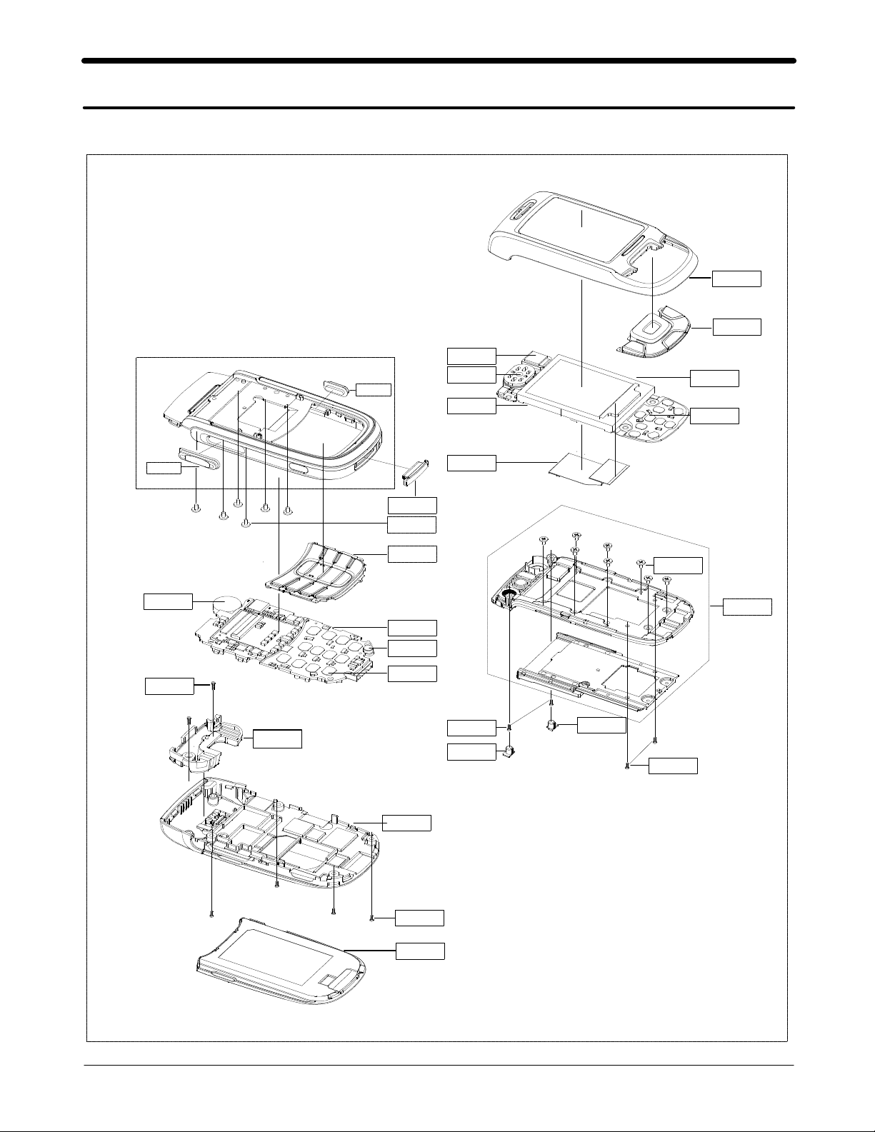
3. SGH-D500 Exploded View and its Parts list
1. Cellular phone Exploded View-1
QCA01
QSP01
QCK01
QMP02
QFU01
QKP02
QLC01
QME02
QVO01
QMO01
QCR11
QAN02
QIF01
QCR08
QKP01
QMP01
QMI01
QME01
QRE01
QPC01
QCR11
QSC16
QCR16
QFL01
QSC18
QCR16
QCR11
QBA19
3-1
SAMSUNG Proprietary-Contents may change without notice
This Document can not be used without Samsung's authorization
2. Cellular phone Parts list
Exploded view and its Part list
Location
NO.
QBA19 BATTERY GH43-01534D
QMP01 MAIN PBA GH92-01852A
QMO01 MOTOR 3101-001411
QMI01 MICROPHONE ASSY GH30-00149A
QME01 UNIT METAL DOME GH59-01697A
QSP01 SPEAKER 3001-001636
QCR08 SCREW 6001-001456
QCR11 SCREW 6001-001654
QCR16 SCREW 6001-001878
QLC01 LCD GH07-00611A
QPC01 PCB FPCB GH41-00700A
QCA01 UNIT CAMERA GH59-01635A
QSC16 PMO-S/L SCREW CAP(L) GH72-17899A
QSC18 PMO-S/L SCREW CAP(R) GH72-17900A
QFU01 SLIDE UPPER GH75-05621A
QFR01 FONT COVER GH75-05622A
QVO01 KEY VOL GH75-05626A
QCK01 CAM GH75-05627A
QFL01 SLIDE LOWER GH75-05623A
QCR16 SCREW 6001-001823
QKP01 KEYPAD MAIN GH75-05624A
QKP02 KEYPAD SUB GH75-05625A
QMP02 SUB PBA GH92-01853A
QME02 UNIT METAL DOME GH59-01698A
QCR11 SCREW 6001-001654
QAN02 INTENNA GH42-00479A
QRE01 REAR COVER GH75-05642A
QCR11 SCREW 6001-001654
QIF01 IF COVER GH72-17901A
Description SEC CODE Remark
3-2
SAMSUNG Proprietary-Contents may change without notice
This Document can not be used without Samsung's authorization

Exploded view and its Part list
3. Test Jig (GH80-01909A)
3-1. RF Test Cable
(GH39-00283A)
3-4. Power Supply Cable
3-2. Test Cable
(GH39-00337C)
3-5. DATA CABLE
(GH39-00331A]
3-3. Serial Cable
3-6. TA
(GH44-00482A)
3-2
SAMSUNG Proprietary-Contents may change without notice
This Document can not be used without Samsung's authorization
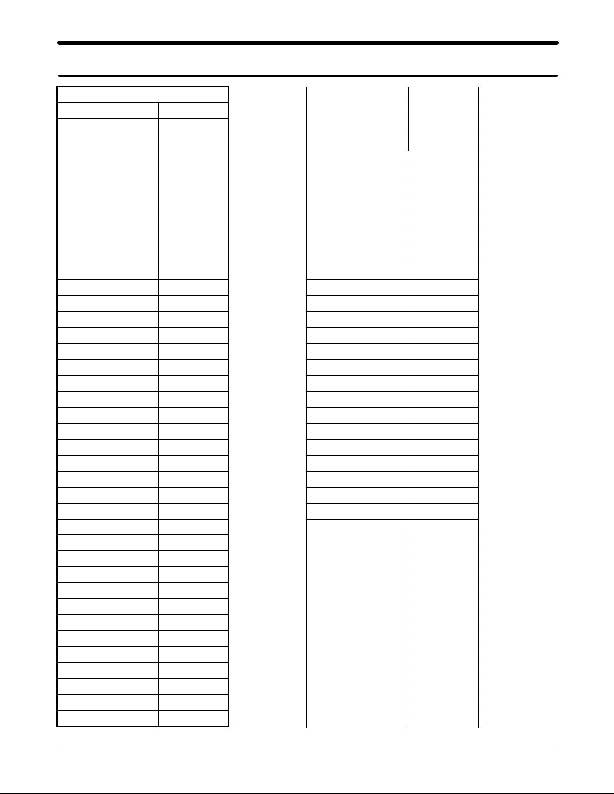
4. SGH-D500 Electrical Parts List
MAIN
SEC CODE Design LOC
0403-001387 ZD500
0403-001427 ZD501
0404-001172 D400
0404-001172 D401
0406-001104 ZD601
0406-001188 U500
0406-001190 ZD600
0407-001002 D600
0504-001113 Q500
0504-001113 Q505
0504-001113 Q506
0504-001151 U506
0505-001332 U306
0505-001518 Q200
0505-001938 U505
0601-001819 LED600
0601-001819 LED601
0601-001819 LED602
0601-001819 LED603
0601-001819 LED604
0601-001819 LED605
0601-001819 LED606
0601-001819 LED607
0601-001819 LED610
0601-001819 LED611
0604-001291 U301
0801-002237 U302
0801-002237 U308
0801-002294 U401
1001-001231 U601
1001-001231 U602
1001-001231 U604
1001-001231 U661
1001-001253 U662
1009-001010 U600
1109-001322 U307
1201-002213 PAM100
1202-001068 U663
1203-002837 U402
1203-003079 U403
1203-003079 U610
1203-003079 U665
1203-003568 U400
1203-003577 U503
1204-002138 U300
1205-002633 U102
1205-002636 U200
1404-001221 V500
1405-001082 TH600
1405-001082 TH601
1405-001082 V300
1405-001082 V301
1405-001082 V302
1405-001082 V303
1405-001082 V400
2007-000137 R510
2007-000138 R622
2007-000140 R602
2007-000140 R604
2007-000143 R210
2007-000143 R315
2007-000143 R316
2007-000147 R216
2007-000148 R101
2007-000148 R111
2007-000148 R201
2007-000148 R212
2007-000148 R300
2007-000148 R304
2007-000148 R312
2007-000148 R504
2007-000151 R314
2007-000152 C500
2007-000160 R515
2007-000162 R206
2007-000162 R207
2007-000162 R208
2007-000162 R209
4-1
SAMSUNG Proprietary-Contents may change without notice
This Document can not be used without Samsung's authorization

4. SGH-D500 Electrical Parts List
2007-000162 R308
2007-000162 R321
2007-000162 R323
2007-000162 R324
2007-000162 R406
2007-000162 R420
2007-000162 R421
2007-000162 R501
2007-000162 R503
2007-000162 R508
2007-000162 R509
2007-000162 R520
2007-000162 R600
2007-000162 R608
2007-000162 R621
2007-000162 R627
2007-000170 R516
2007-000170 R517
2007-000171 L200
2007-000171 R100
2007-000171 R112
2007-000171 R113
2007-000171 R114
2007-000171 R115
2007-000171 R120
2007-000171 R202
2007-000171 R310
2007-000171 R318
2007-000171 R320
2007-000171 R325
2007-000171 R404
2007-000171 R411
2007-000171 R412
2007-000172 R103
2007-000242 R204
2007-000242 R205
2007-000566 R102
2007-000566 R104
2007-000758 R500
2007-000758 R502
2007-000831 R313
2007-000831 R620
2007-000932 R116
2007-000932 R118
2007-001217 R610
2007-001217 R611
2007-001217 R612
2007-001217 R613
2007-001217 R616
2007-001217 R617
2007-001217 R623
2007-001217 R624
2007-001217 R625
2007-001217 R626
2007-001288 R106
2007-001303 R305
2007-001313 R107
2007-001313 R108
2007-001325 R307
2007-001333 R511
2007-001339 R609
2007-002796 R413
2007-002796 R605
2007-003001 R117
2007-007009 R328
2007-007009 R329
2007-007014 R303
2007-007014 R326
2007-007090 R409
2007-007100 R403
2007-007107 R506
2007-007136 R512
2007-007193 R327
2007-007318 R514
2007-007334 R402
2007-007480 R619
2007-007573 R618
2007-007592 R401
2007-007861 R507
2007-008117 R513
4-2
SAMSUNG Proprietary-Contents may change without notice
This Document can not be used without Samsung's authorization
4. SGH-D500 Electrical Parts List
2203-000233 C108
2203-000233 C113
2203-000233 C114
2203-000233 C129
2203-000233 C151
2203-000233 C300
2203-000233 C428
2203-000254 C140
2203-000254 C148
2203-000254 C201
2203-000254 C323
2203-000254 C625
2203-000254 C626
2203-000278 C600
2203-000278 C611
2203-000278 C622
2203-000330 R603
2203-000425 C120
2203-000425 C122
2203-000425 C633
2203-000425 C634
2203-000438 C304
2203-000438 C623
2203-000438 C710
2203-000438 C711
2203-000466 C138
2203-000585 C143
2203-000628 C135
2203-000628 C404
2203-000654 C144
2203-000679 C133
2203-000679 C301
2203-000679 C317
2203-000679 C607
2203-000725 C326
2203-000812 C102
2203-000812 C112
2203-000812 C119
2203-000812 C124
2203-000812 C150
2203-000812 C204
2203-000812 C210
2203-000812 C411
2203-000812 C705
2203-000812 C716
2203-000812 C717
2203-000812 C718
2203-000812 C719
2203-000812 C755
2203-000812 C756
2203-000854 C104
2203-000854 C115
2203-000854 C121
2203-000854 C137
2203-000854 C141
2203-000995 C103
2203-000995 C105
2203-000995 C619
2203-001153 C608
2203-001178 L108
2203-001201 C109
2203-001201 C319
2203-001259 C618
2203-001437 C628
2203-001437 C629
2203-002443 C604
2203-002525 C313
2203-003054 C407
2203-003054 C409
2203-003054 C630
2203-003054 C635
2203-005050 C606
2203-005057 C110
2203-005061 C715
2203-005446 C131
2203-005480 C315
2203-005482 C111
2203-005482 C117
2203-005482 C118
2203-005482 C202
4-3
SAMSUNG Proprietary-Contents may change without notice
This Document can not be used without Samsung's authorization

4. SGH-D500 Electrical Parts List
2203-005482 C203
2203-005482 C205
2203-005482 C207
2203-005482 C208
2203-005482 C211
2203-005482 C212
2203-005482 C213
2203-005482 C214
2203-005482 C216
2203-005482 C302
2203-005482 C305
2203-005482 C308
2203-005482 C309
2203-005482 C312
2203-005482 C314
2203-005482 C316
2203-005482 C321
2203-005482 C322
2203-005482 C324
2203-005482 C325
2203-005482 C327
2203-005482 C405
2203-005482 C420
2203-005482 C503
2203-005482 C603
2203-005482 C605
2203-005482 C609
2203-005482 C613
2203-005482 C621
2203-005482 C624
2203-005482 C631
2203-005509 C501
2203-005512 C311
2203-006053 C310
2203-006053 C400
2203-006053 C401
2203-006090 C402
2203-006190 C123
2203-006208 C200
2203-006208 C413
2203-006208 C416
2203-006208 C419
2203-006208 C424
2203-006208 C425
2203-006208 C615
2203-006208 C616
2203-006208 C620
2203-006208 C720
2203-006208 C721
2203-006257 C306
2203-006257 C307
2203-006257 C406
2203-006257 C414
2203-006257 C417
2203-006257 C418
2203-006257 C426
2203-006257 C427
2203-006257 V700
2203-006474 C429
2203-006474 C430
2404-001268 C502
2404-001281 C410
2404-001281 C601
2404-001348 C125
2404-001386 C303
2503-001053 C766
2503-001053 C767
2503-001053 C768
2503-001053 C769
2503-001053 C770
2503-001053 C771
2503-001053 C772
2503-001053 C773
2503-001053 C774
2703-001722 L101
2703-001723 L103
2703-001723 L116
2703-001723 R405
2703-001724 L301
2703-001749 L100
4-4
SAMSUNG Proprietary-Contents may change without notice
This Document can not be used without Samsung's authorization
4. SGH-D500 Electrical Parts List
2703-001752 L300
2703-001913 L600
2703-001913 L601
2703-002199 C149
2703-002199 L105
2703-002199 L107
2703-002204 L102
2703-002268 L110
2703-002281 L104
2703-002281 L117
2703-002320 L118
2703-002346 L401
2703-002636 L106
2801-003856 OSC400
2809-001294 U101
2901-001254 U103
2901-001315 U501
2904-001537 F101
2904-001540 F102
2904-001552 F100
2904-001553 F103
2909-001269 U100
3301-001120 L400
3301-001534 F600
3301-001729 R119
3404-001152 SW700
3404-001152 SW701
3404-001152 SW702
3705-001347 RFS100
3708-002054 CN701
3709-001355 SIM400
3710-001611 IFC500
3711-005829 BTC500
3722-002269 CN600
4202-001031 ANT300
4302-001180 C408
4709-001349 U304
GH13-00025A U305
GH71-04302A ANT104
GH71-04302A ANT105
SUB
SEC CODE Design LOC
0404-001262 ZD801
0501-002440 Q802
0504-001140 Q801
0505-001889 U804
0601-001819 LED801
0601-001819 LED805
0601-001819 LED806
0601-001819 LED807
0601-001819 LED808
0601-001819 LED810
0601-001990 LED811
1203-003328 U802
1203-003564 U803
1405-001082 R829
1405-001082 V800
1405-001082 V801
1405-001082 V802
1405-001082 V803
1405-001128 V804
1405-001128 V805
2007-000140 R826
2007-000151 R812
2007-000162 R814
2007-000162 R824
2007-000170 R825
2007-000171 R811
2007-000171 R822
2007-000172 R819
2007-003029 R828
2007-003030 R800
2007-003030 R801
2007-003030 R802
2007-003030 R803
2007-003030 R806
2007-003030 R807
2007-007200 R820
2007-007200 R821
2007-007529 R827
4-5
SAMSUNG Proprietary-Contents may change without notice
This Document can not be used without Samsung's authorization
 Loading...