

Samsung SGH-D428 Service Manual

GSM TELEPHONE
SGH-D428
GSM TELEPHONE
CONTENTS
1. Specification
2. Flow Chart of Troubleshooting
3. Exploded Views and Parts List
4. Electrical Parts List
5. Block Diagrams
6. PCB Diagrams
This Service Manual is a property of Samsung Electronics Co.,Ltd.
Any unauthorized use of Manual can be punished under applicable
International and/or domestic law.
ⓒ
Samsung Electronics Co.,Ltd. Dec. 2004
Printed in Korea.
Code No.: GH68-06337A
BASIC.
1. SGH-D428 Specification
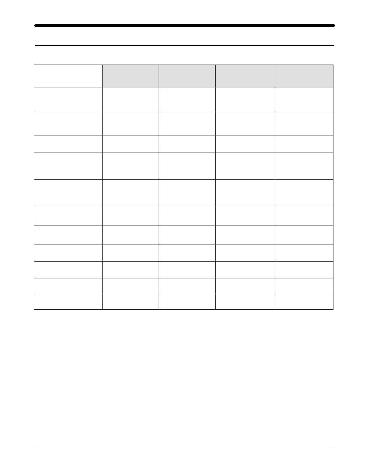
1. GSM General Specification
GSM900
Phase 1
Freq. Band[MHz]
Uplink/Downlink
ARFCN range 1~124
Tx/Rx spacing 45MHz 45MHz 95MHz 80MHz
Mod. Bit rate/
Bit Period
Time Slot
Period/Frame
Period
Modulation 0.3GMSK 0.3GMSK 0.3GMSK 0.3GMSK
MS Power 33dBm~13dBm 33dBm~5dBm 30dBm~0dBm 30dBm~0dBm
890~915
935~960
270.833kbps
3.692us
576.9us
4.615ms
EGSM 900
Phase 2
880~915
925~960
0~124 &
975~1023
270.833kbps
3.692us
576.9us
4.615ms
DCS1800
Phase 1
1710~1785
1805~1880
512~885 512~810
270.833kbps
3.692us
576.9us
4.615ms
PCS1900
1850~1910
1930~1990
270.833kbps
3.692us
576.9us
4.615ms
Power Class 5pcl ~ 15pcl 5pcl ~ 19pcl 0pcl ~ 15pcl 0pcl ~ 15pcl
Sensitivity -102dBm -102dBm -100dBm -100dBm
TDMA Mux 8 8 8 8
Cell Radius 35Km 35Km 2Km -
1-1
SAMSUNG Proprietary-Contents may change without notice
This Document can not be used without Samsung's authorization
SGH-D428 Specification
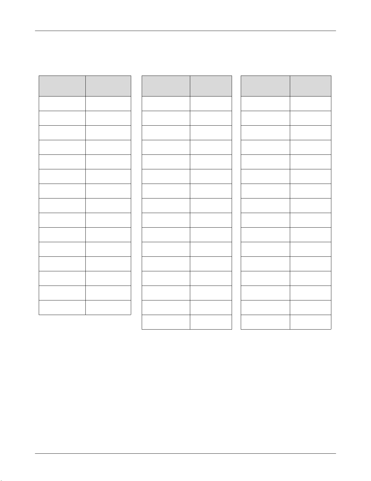
2. GSM TX power class
TX Power
control level
5 33±2dBm
6 31±2dBm
7 29±2dBm
8 27±2dBm
9 25±2dBm
10 23±2dBm
11 21±2dBm
12 19±2dBm
13 17±2dBm
14 15±2dBm
15 13±2dBm
GSM900
TX Power
control level
0 30±3dBm
1 28±3dBm
2 26±3dBm
3 24±3dBm
4 22±3dBm
5 20±3dBm
6 18±3dBm
7 16±3dBm
8 14±3dBm
9 12±4dBm
10 10±4dBm
DCS1800
TX Power
control level
0 30±3dBm
1 28±3dBm
2 26±3dBm
3 24±3dBm
4 22±3dBm
5 20±3dBm
6 18±3dBm
7 16±3dBm
8 14±3dBm
9 12±4dBm
10 10±4dBm
PCS1900
16 11±2dBm
17 9±2dBm
18 7±2dBm
19 5±2dBm
11 8±4dBm
12 6±4dBm
13 4±4dBm
14 2±5dBm
15 0±5dBm
11 8±4dBm
12 6±4dBm
13 4±4dBm
14 2±5dBm
15 0±5dBm
1-2
SAMSUNG Proprietary-Contents may change without notice
This Document can not be used without Samsung's authorization
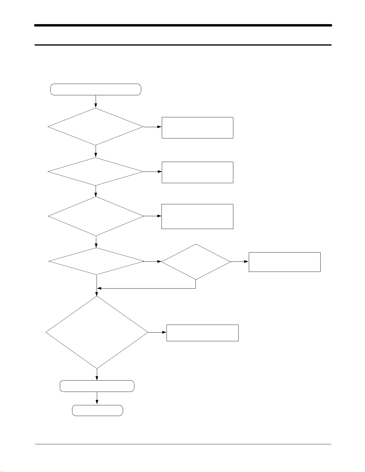
2. SGH-D428 Flow Chart of Troubleshooting
1.Baseband
1. Power ON
'Power On' does not work
Yes
Check the current
consumption more
than 100mA
Yes
Check the VBAT
more than 3.3V
Yes
Check the pin
11 of U102 is
more than 2.8V
Yes
U102 pin 33,39
=2.8V
Yes
No
No
No
No
Download again
Charge the Battery
Check the C117
U102 pin 9
=1.8V
Yes
No
Check U102 and C116
Check the clock
signal at pin4 of
OSC801
Freq=13MHz ?
Vrms≥300mV ?
Vpp is around
900mVpp ?
Yes
Check the initial operation
END
SAMSUNG Proprietary-Contents may change without notice
This Document can not be used without Samsung's authorization
No
Check the clock generation
circuit
2-1
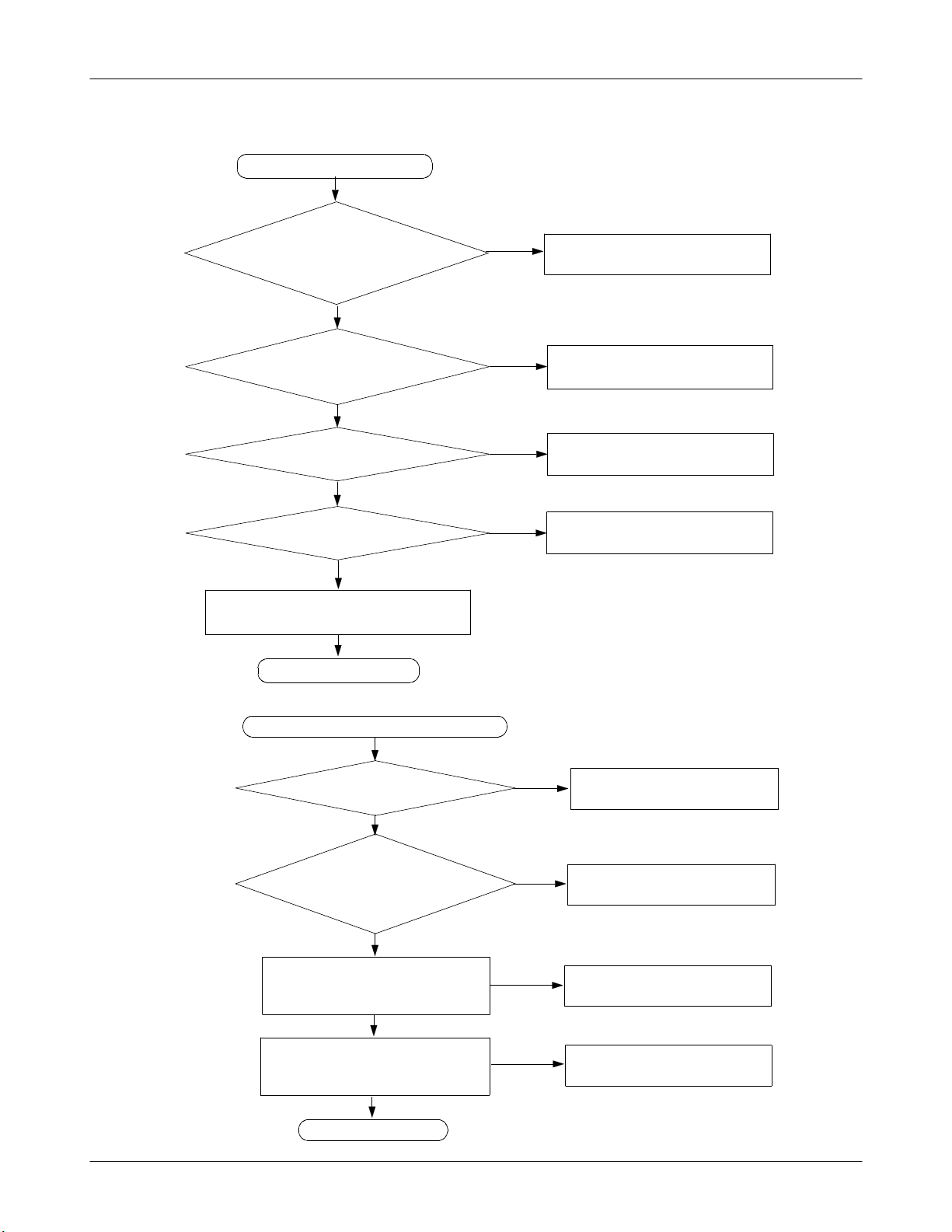
SGH-D428 Flow Chart of Troubleshooting and Circuit Diagrams
2. Initial
Initial Failure
Yes
Check the signal at the
pin 21 of U102 is
"High" when the phone
is boot on
Yes
Checkthekeymetrix
of the U601
Yes
Check the VCCD,VCC_1.8A
Check LCD connector CN201 in the main
PBA and the FPCB connector
of U601
Yes
Check the vccd of
U601 is around 2.8V
Yes
Yes
END
No
No
No
No
Check the pin 46,20 and Q103
Check the key program and
the key pcb
Check the soldered status of U601,
OSC601
Check the soldered status of
U601,osc601
3. Sim Part
Phone can't access SIM card
Yes
Check the pin 1 of
CN101. voltage 3V ?
Yes
Check the SIM
connector's (CN101)
connection to SIM
card
Yes
Check the circuit around CN101
Check the circuit around U601
and vlotage supply circuitry
input
circuitry
Yes
output
Yes
END
2-2
No
No
No
No
Check the circuit related to
U102
Resolder or change CN101
Check the related circuit of
CN101
Check the related circuit of
U601 and U102
SAMSUNG Proprietary-Contents may change without notice
This Document can not be used without Samsung's authorization
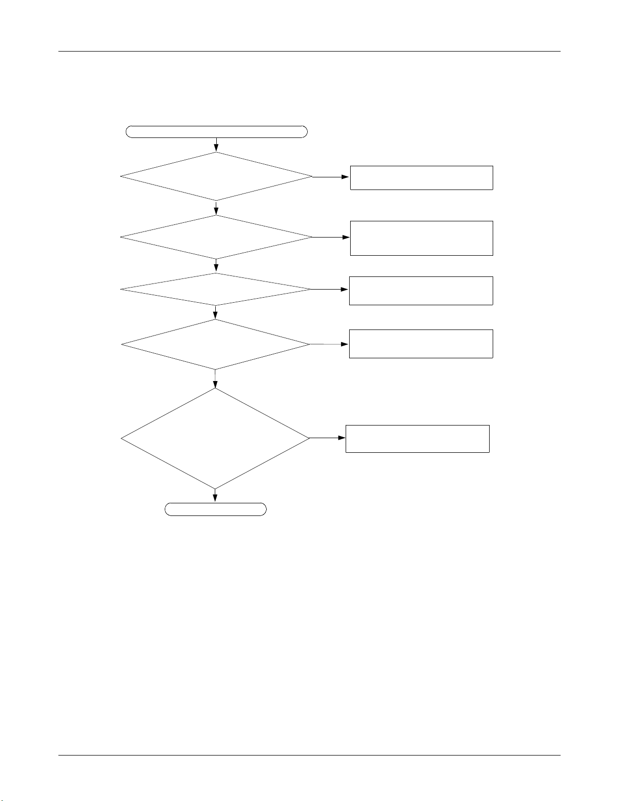
4. Charging Part
Abnormal charging part
SGH-D428 Flow Chart of Troubleshooting and Circuit Diagrams
Yes
Check the pin 17, 18
of CN300 is
TA_VEXT>4?
Yes
Check the pin 2 of
U101 is "low"?
Yes
Check the pin 3 of
Q101 is "low"?
Yes
Check the pin 5 of
U101 is "3.2~4.2V"?
Yes
Check the ICHRG is
1V(during charging)
and around
180mV(full charging)?
No
No
No
No
No
Replace TA,Check CN300-1
Check the U101
Check the Q101
Check the U101
Resolder or change R111
Yes
END
2-3
SAMSUNG Proprietary-Contents may change without notice
This Document can not be used without Samsung's authorization
SGH-D428 Flow Chart of Troubleshooting and Circuit Diagrams
5. Microphone Part
Microphone does not work
Yes
6. Speaker Part
Speaker does not work
check the soldered
status of microphone.
Yes
Check the reference
voltage on mic path
C411≒2.5 V
Yes
Is microphone ok?
Yes
END
No
No
No
Resolder microphone
Resolder or change
R413,C420,R414,C410,R411,R40
8
Check U701
Yes
Check the FPCB from
CN201 to CN11
Yes
Check the PIN 4 of
U401='High' ?
Yes
Is speaker ok?
Yes
Is speaker ok?
Yes
END
No
No
No
No
Retry connection the FPCB from
Check componants near the U402
CN201 to CN11
Check U401 and the audio
path of U701
and control line of U402
Change Speaker
2-4
SAMSUNG Proprietary-Contents may change without notice
This Document can not be used without Samsung's authorization

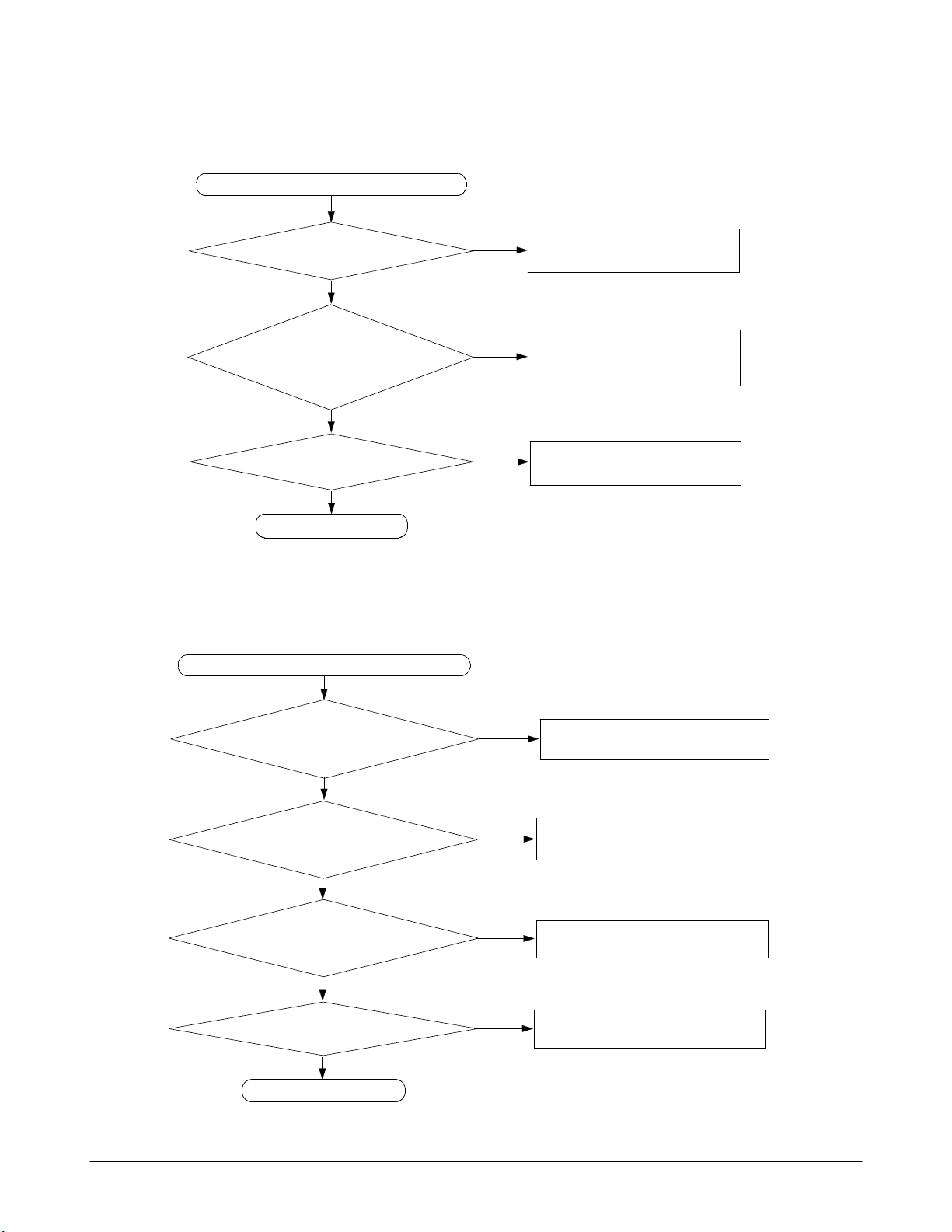
2.RF
1. EGSM RX
NORMAL CONDITION
catch the channel?
pin13≥-65dBm ?
pin1, 2≥-65dBm ?
YES
F1001 CHECK
YES
F1001 CHECK
YES
NO
NO
NO
SGH-D428 Flow Chart of Troubleshooting and Circuit Diagrams
CONTINUOUS RX ON
RF INPUT : 62CH
CHECK
ANT1001,L1002 contact ?
C1003, C1006
resolder or change
F1001
resolder or change
AMP : -50dBm
U1002 CHECK
pin20,21≥-65dBm ?
YES
U902
pin 26,32: 2.8V ?
YES
U903 CHECK
pin 7 : 13MHz ?
Vp-p : 950mV?
YES
U902
pin1,2,5,6 Vp-p
:120mV?
YES
U702,R701
resolder or change
NO
NO
NO
NO
U102 pin39, C112
change or resolder
OSC801
change or resolder
resolder or change
C1005,C1006,L1003
resolder or change
U902
2-5
SAMSUNG Proprietary-Contents may change without notice
This Document can not be used without Samsung's authorization
SGH-D428 Flow Chart of Troubleshooting and Circuit Diagrams
2. DCS RX
NORMAL CONDITION
catch the channel?
YES
NO
CHECK
ANT1001,L1002 contact ?
CONTINUOUS RX ON
RF INPUT : 698CH
AMP : -50dBm
F1001 CHECK
pin13≥-65dBm ?
YES
F1001 CHECK
pin3, 4≥-65dBm ?
YES
U902 CHECK
pin21,22≥-65dBm ?
YES
U902
pin 26,32: 2.8V ?
YES
U903 CHECK
pin 7 : 13MHz ?
Vp-p : 950mV?
YES
U902
pin1,2,5,6 Vp-p
:120mV?
NO
NO
NO
NO
NO
NO
U102 pin39, C112
change or resolder
change or resolder
resolder or change
C1008,C1009
resolder or change
F1001
resolder or change
C1008,C1009,L1004
resolder or change
OSC801
U902
YES
U703,R704
resolder or change
This Document can not be used without Samsung's authorization
2-6
SAMSUNG Proprietary-Contents may change without notice

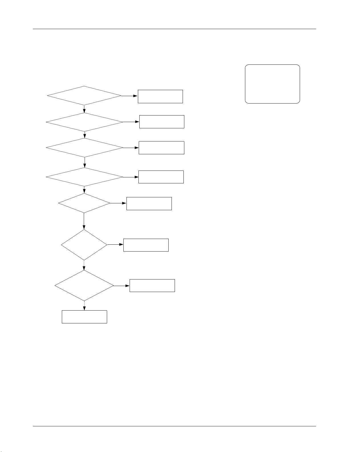
3. PCS RX
NORMAL CONDITION
catch the channel?
YES
F1001 CHECK
pin13≥-65dBm ?
YES
F1001,F1002 CHECK
pin6≥-65dBm ?
YES
NO
NO
NO
SGH-D428 Flow Chart of Troubleshooting and Circuit Diagrams
CONTINUOUS RX ON
RF INPUT : 660CH
CHECK
ANT1001,L1002 contact ?
C1012, F1013
resolder or change
F1001,F1002,R1011
resolder or change
AMP : -50dBm
U902 CHECK
pin16, 17≥-65dBm ?
YES
U902
pin 26,32: 2.8V ?
YES
U903 CHECK
pin 7 : 13MHz ?
Vp-p : 950mV?
YES
U902
pin1,2,5,6 Vp-p
:120mV?
YES
U704,R705
resolder or change
NO
NO
NO
NO
U102 pin39, C112
change or resolder
change or resolder
C1012,F1002,C1013,R1011,L1006
resolder or change
OSC801
U902
resolder or change
2-7
SAMSUNG Proprietary-Contents may change without notice
This Document can not be used without Samsung's authorization

SGH-D428 Flow Chart of Troubleshooting and Circuit Diagrams
4. EGSM TX
F1001 pin 12 :
about 2~3
F1003, C1003
check&change
NO
YES
U1001
pin 5 : 3.7 V?
YES
U1001
pin 6 : 1.2V ?
U1001 pin7
about : -5dBm ?
NO
NO
YES
YES
F1001
pin13:2.8V?
U1001 pin9 :
about 4~5dBm?
F1001,C1015
check & change
NO
BATTERY, U102
check & change
NO
YES
YES
U701
check
NO
U701,U702
check & change
CONTINUS TX ON CONDITION
TX POWER DAC: 550 CODE APPLIED
CH : 62
RBW : 100KHz
VBW : 100KHz
SPAN : 10MHz
REF LEV. : 10dBm
ATT. : 20dB
U102 pin39,C112
change or resolder
U1001
pin 3 : 3V?
YES
U1001
change or resolder
NO
change or resolder
NO
U701
check
U902
pin14,26,32 : 2.
8V ?
NO
U701
YES
U903
pin7 : 13MHz ?
Vp-p : 950mV?
U902
pin1,2,4,5:100m
U902
change or resolder
YES
YES
NO
change or resolder
OSC801
2-8
SAMSUNG Proprietary-Contents may change without notice
This Document can not be used without Samsung's authorization
 Loading...