

Samsung SGH-C300 Service Manual
GSM TELEPHONE
SGH-C300
GSM TELEPHONE
CONTENTS
1. Specification
2. Exploded View and Parts list
3. Chart of Troubleshooting
4. Array course control
5. Block Diagrams
6. PCB Diagrams
7. MAIN Electrical Parts List
8. Reference data
9. Safety Precautions
10. Product Function

Contents
1. Specification
1-1. GSM/CDMA General Specification ...........................................................................1-1
1-2. GSM TX power class ...............................................................................................1-2
2. Exploded View and Parts list
2-1. Cellular phone Exploded View ..................................................................................2-1
2-2. Cellular phone Parts list ............................................................................................2-2
2-3. Disassembly ...............................................................................................................2-4
2-4. Assembly ....................................................................................................................2-6
3. Flow Chart of Troubleshooting
3-1. Baseband ....................................................................................................................3-1
3-1-1. Power ON .............................................................................................................3-1
3-1-2. Initial ......................................................................................................................3-5
3-1-3. SIM Part ................................................................................................................3-8
3-1-4. Microphone Part ..................................................................................................3-10
3-1-5. Receiver Part ......................................................................................................3-12
3-1-6. Speaker Part .......................................................................................................3-12
3-2. RF .............................................................................................................................3-15
3-2-1. EGSM Rx ............................................................................................................3-15
3-2-2. DCS Rx ...............................................................................................................3-17
3-2-3. EGSM TX ............................................................................................................3-19
3-2-4. DCS TX ...............................................................................................................3-21
4. Array course control
4-1. Downloading Binary Files ......................................................................................4-2
4-2. Pre-requsite for Downloading ................................................................................4-2
4-3. S/W Downloader Program .....................................................................................4-3
5. Block Diagrams
6. PCB Diagrams

Contents
7. MAIN Electrical Parts List
8. Reference data
8-1. Reference Abbreviate ..............................................................................................8-1
9. Safety Precautions
9-1. Repair Precaution ......................................................................................................9-1
9-2. ESD(Electrostaically Sensitive Devices) Precaution ................................................9-2
10. Product Function
1. Specification
1-1. GSM General Specification
GSM 900
Phase 1
Freq. Band[MHz]
Uplink/Downlink
ARFCN range 1~124
Tx/Rx spacing 45 MHz 45 MHz 95 MHz
Mod. Bit rate/
Bit Period
Time Slot Period/Frame
Period
Modulation 0.3 GMSK 0.3 GMSK 0.3 GMSK
MS Power 33 dBm~13 dBm 33 dBm~5 dBm 30 dBm~0 dBm
Power Class 5pcl~15pcl 5pcl~19pcl 0pcl~15pcl
Sensitivity -102 dBm -102 dBm -100 dBm
890~915
935~960
270.833 Kbps
3.692 us
576.9 us
4.615 ms
EGSM 900
Phase 2
880~915
925~960
0~124 &
975~1023
270.833 Kbps
3.692 us
576.9 us
4.615 ms
270.833 Kbps
DCS1800
Phase 1
1710~1785
1805~1880
512~885
3.692 us
576.9 us
4.615 ms
TDMA Mux 8 8 8
Cell Radius 35 Km 35 Km 2 Km
1-1
Specification
1-2. GSM TX power class
TX Power
control level
533±2dBm
631±2dBm
729±2dBm
827±2dBm
925±2dBm
10 23±2 dBm
11 21±2 dBm
12 19±2 dBm
13 17±2 dBm
14 15±2 dBm
15 13±2 dBm
GSM900
TX Power
control level
0 30±3 dBm
1 28±3 dBm
2 26±3 dBm
3 24±3 dBm
4 22±3 dBm
5 20±3 dBm
6 18±3 dBm
7 16±3 dBm
8 14±3 dBm
9 12±4 dBm
10 10±4 dBm
DCS1800
16 11±3 dBm
17 9±3 dBm
18 7±3 dBm
19 5±3 dBm
11 8±4 dBm
12 6±4 dBm
13 4±4 dBm
14 2±5 dBm
15 0±5 dBm
1-2
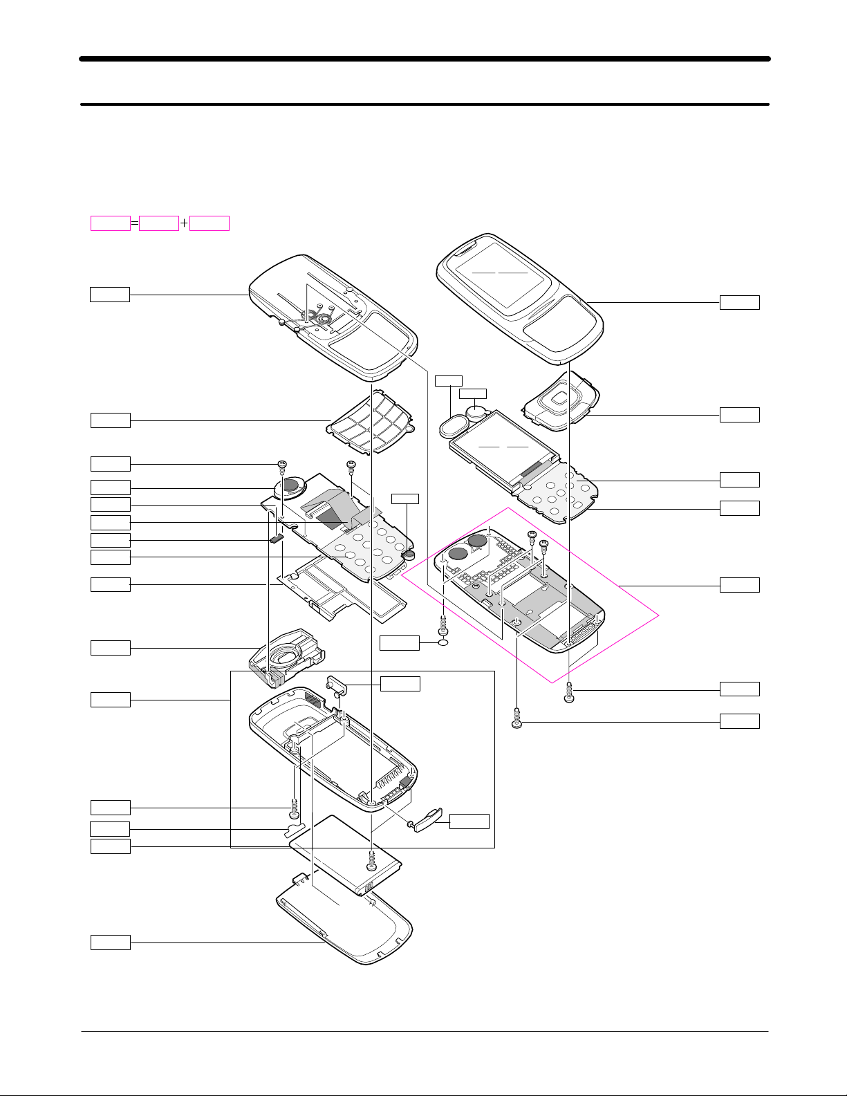
2. Exploded View and Parts List
2-1. Cellular phone Exploded View
QHI01
QFR01
QKP01
QCR05
QSP01
QMP01
QPC01
QAN05
QME01
QRE02
QFR01 QFL01
QMI01
QFU01
QAR01
QMO01
QKP02
QME02
QLC01
QFL01
QAN02
QRE01
QCR05
QRF01
QBA01
QBA00
QSC01
QRF03
QCR05
QCR06
QIF01
2-1
SAMSUNG Proprietary-Contents may change without notice
This Document can not be used without Samsung's authorization

Exploded View and Parts List
2-2. Cellular phone Parts list
Design LOC Discription SEC CODE
QAN02
QAN05
QAR01
QBA00
QBA01
QCR05
QCR05
QCR05
QCR06
QFU01
QKP01
QKP02
QLC01
QME01
QME02
QMI01
QMO01
QMP01
QPC01
QRE02
QRF01
QSC01
QSP01
QHI01
QRE01
INTENNA-SGHC300 GH42-01026A
ASSY MEC-INTENNA CONTACT GH75-08168A
AUDIO-RECEIVER 3009-001248
PMO-COVER BATT GH72-35005A
INNER BATTERY PACK-800MAH,MAIN GH43-02589A
SCREW-MACHINE 6001-001478
SCREW-MACHINE 6001-001478
SCREW-MACHINE 6001-001478
SCREW-MACHINE 6001-001155
ASSY COVER-SLIDE UPPER GH98-02593A
ASSY KEYPAD-MAIN(RUSS/BLK) GH98-03231A
ASSY KEYPAD-SUB(OPEN/SIL) GH98-02701A
ELA UNIT-SGHC300 LCD MODULE KI GH96-02439A
UNIT-DOME SHEET (F/K) GH59-03770A
UNIT-DOME SHEET (N/K) GH59-03769A
MICROPHONE-ASSY-SGHC300 GH30-00323A
MOTOR-DC 3101-001324
PBA MAIN-SGHC300 (PBA MAIN) GH92-03086A
MEA-SLIDE FPCB KIT GH97-06882A
ASSY BRACKET-REAR GH98-02598A
MPR-TAPE SHEET RF GH74-28478A
MPR-TAPE COVER SHEET SCREW GH74-28472A
SPEAKER 3001-002083
ASSY HINGE-SLIDE GH98-02594A
QFL01 ASSY COVER-SLIDE LOWER GH98-02595A
QFR01 ASSY CASE-FRONT GH98-02596A
ASSY CASE-REAR GH98-02597A
QRF03 PMO-COVER EAR GH72-35003A
QIF01 PMO-COVER IF GH72-35004A
2-2
SAMSUNG Proprietary-Contents may change without notice
This Document can not be used without Samsung's authorization
Exploded View and Parts List
Discription SEC CODE
BAG PE 6902-000297
ADAPTOR-EU 220V TYPE(BLK) GH44-01334A
LABEL(P)-WATER SOAK GH68-02026A
LABEL(P)-WATER SOAK GH68-02026A
MANUAL-SFC GH68-04336A
LABEL(P)-BARCODE RUSSIA GH68-08494A
MANUAL USERS-EU RUSSIAN GH68-12796A
LABEL(R)-MAIN(SER) GH68-13315B
BOX(P)-UNIT MAIN(SER) GH69-04832B
PMO-COVER SLIDE WINDOW GH72-35006A
RMO-RUBBER CSP GH73-08597A
RMO-RUBBER LCD PBA GH73-08818A
MPR-GASK TAPE GH74-24020A
MPR-TAPE IF COVER GH74-24740A
MPR-GASK TAPE GH74-24796A
MPR-SPONGE INTENNA GH74-28468A
MPR-TAPE SLIDE WINDOW GH74-28470A
MPR-VINYL BOHO WINDOW GH74-28851A
MPR-SPONGE MAIN PCB GH74-29058A
MPR-SPONGE LCD FPCB GH74-29059A
MPR-TAPE ESD GH74-29066A
MPR-TAPE FPCB BACK B GH74-29067A
MPR-SPONGE KEYPAD GH74-29255A
MPR-SPONGE KEYPAD GH74-29255A
MPR-INSU TAPE GH74-29334A
MPR-ELEC TAPE GH74-29335A
MPR-INSU TAPE GH74-29352A
MPR-INSU TAPE GH74-29352A
MPR-SPONGE SPK GH74-29444A
MPR-SPONGE GH74-29579A
2-3
SAMSUNG Proprietary-Contents may change without notice
This Document can not be used without Samsung's authorization

Exploded View and Parts List
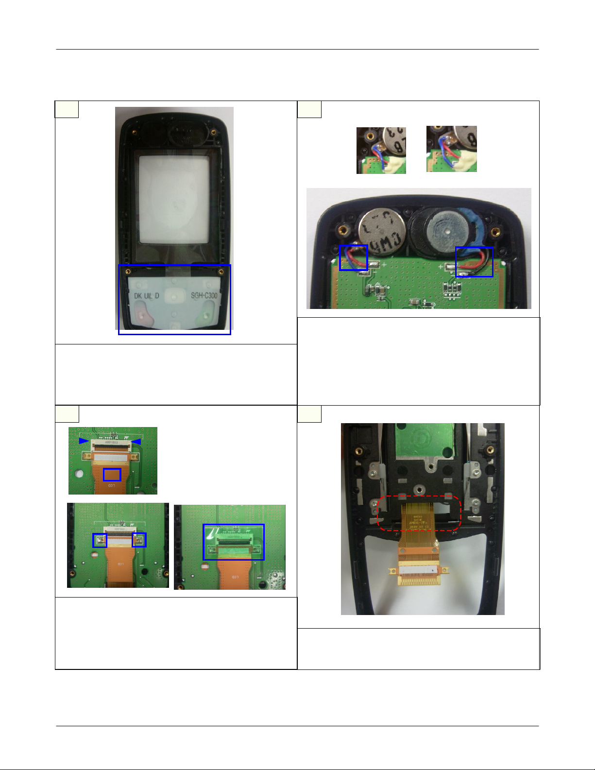
2-3. Disassembly
1
1)Disjoint the REAR screw of 4 points.
※
caution
1) Be careful of scratch.
2
1) After get out the cover of earjack and IF connector
cover, disjoint REAR's lower locker and upper locker
as a picture below.
※
caution
1) Be careful of scratch.
1) Disjoint two lockers assembled with PBA.
※
caution
1) Be careful of the damage of devices.
43
1) Remove the green tape on the FPCB with
tweezers.
2) Disjoint the FPCB by desoldering.
※
caution
1) Be careful of the FPCB's crack
2-4
SAMSUNG Proprietary-Contents may change without notice
This Document can not be used without Samsung's authorization

Exploded View and Parts List
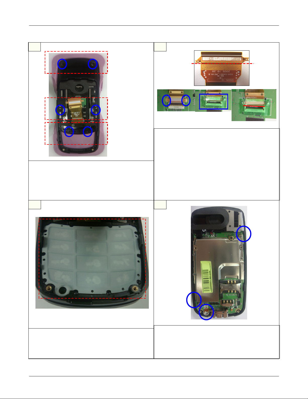
5
1) Disjoint 6 screws.
※
caution
1) Be careful of scratch.
2) Use the '+' screwdriver.
M1.4*L3.0
M1.4*L3.5
M1.4*L3.0
6
1) Disjoint HINGE ASS'Y as a picture below
※
caution
1) Be careful of the damage of FPCB
1) Remove the green tape from the FPCB
2) Disjoint the FPCB with desoldering.
※
caution
1) Be careful of the FPCB's crack.
87
1) Remove the motor with tweezers.
2) Remove the receiver with tweezers.
※
caution
1)Be careful of the damages of motor and receiver
wires.
2-5
SAMSUNG Proprietary-Contents may change without notice
This Document can not be used without Samsung's authorization
Exploded View and Parts List
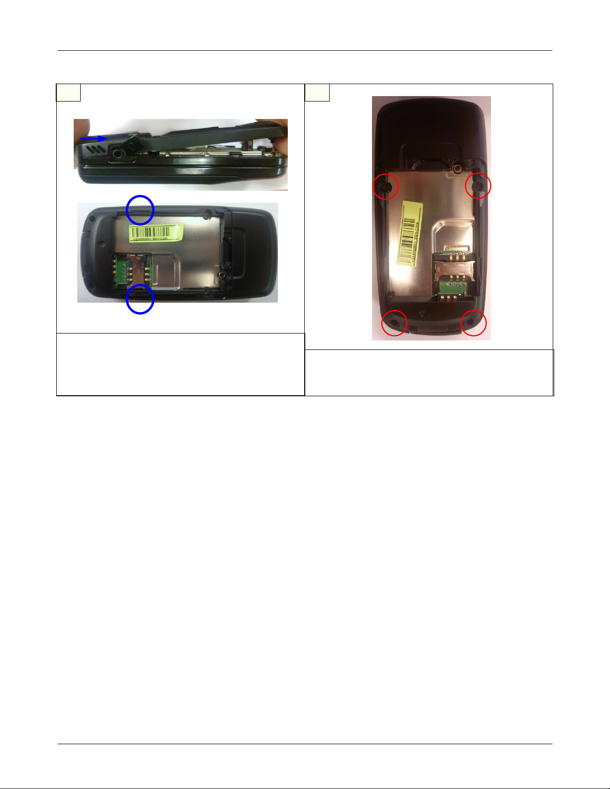
2-4. Assembly
1
1) Assemble the SUB KEYPAD on UPPER as
picture below.
※
caution
1) Put the holes around 3*4 KEY on the UPPER.
2
<Bad>
1) Put the SUB PBA on the UPPER with LCD's
guide holes.
2) Insert the motor and receiver on each places.
※
caution
1) Be careful of overlap the wires.
2) Be careful of the damage of wires.
< Good >
1) After inserting the LCD FPCB in the connector,
soldering it and attach the green tape.
※
caution
1) Be careful of the scratch on the plastic.
2) Be careful of the crack on LCD FPCB.
43
1) Insert the MAIN FPCB as picture below.
※
caution
1) Be careful of the crack on LCD FPCB.
2-6
SAMSUNG Proprietary-Contents may change without notice
This Document can not be used without Samsung's authorization
Exploded View and Parts List
5
M1.4*L3.0
M1.4*L3.5
M1.4*L3.0
1) Screw up the 6 points with SLIDE JIG.
※
caution
1) Fix the handset on the JIG not to move it down
the Slide.
2) Screw up right size.
6
1) Fold the FPCB as the picture below.
2) Insert the LCD FPCB to the connector along the
SILK LINE, soldering and attach the green tape,
double sticky tape.
3) Move out the cover of the tape. Fold the FPCB
and push that place.
※
caution
1) Be careful of the damage of FPCB.
2) Attach double sticky tape with white silk line.
1) Assemble the 3*4 Keypad as picture below.
※
caution
1) Be careful of the 3*4 KEY PAD escaping from
the holes.
87
1) After locking the PAB to the two hooks, insert
themicrophoneintotheholder.
※
caution
1) Be careful of the damage of the devices.
2) Be careful of MIC escaping from the KEY PAD.
2-7
SAMSUNG Proprietary-Contents may change without notice
This Document can not be used without Samsung's authorization
Exploded View and Parts List
9
1) At first,assemble the REAR's upper and joint the
lower with pushing two lockers.
※
caution
1)Be careful of the scratch on the plastic.
10
1) Screw up the 4 points with SCREW JIG.
※
caution
1)Be careful of the scratch on the plastic.
2-8
SAMSUNG Proprietary-Contents may change without notice
This Document can not be used without Samsung's authorization
3. Flow Chart of Troubleshooting
3-1.Baseband
3-1-1. Power ON
'Power On' does not work
Check the current consumption
Yes
Current consumption
>= 100mA
Yes
Check the Vbat Voltage
Voltage >=3.3V
Yes
Check the pin of UCP100
Pin#J12 >= 2.8V
Yes
Pin#A13 and pin#A14
=2.8V
Yes
Check the clock signal at pin#21 of U400
No
No
No
No
Download again
Charge the Battery
Check UCP100 and C115
pin#G11 = 1.8V
Yes
No
Check UCP100 and C116
Freq = 26MHz
Vrms >=300mV
Vpp≒900mV
Yes
Check the clock signal at pin#5,#6 of U401
Freq = 13Mz
Yes
Check the initial operation
END
SAMSUNG Proprietary-Contents may change without notice
This Document can not be used without Samsung's authorization
No
No
Check the clock generation circuit
(related to OSC400)
Check U401
3-1

Flow Chart of Troubleshooting
3-2
SAMSUNG Proprietary-Contents may change without notice
This Document can not be used without Samsung's authorization

Flow Chart of Troubleshooting
V9.2_FRV
004CSO
414C
514C
1DNG
TOH3
2DNG4
2
TOH
1
TUO_M62
CFA PQXTR
204R
024C
124C
V9.2_DCCV
7
8
1
TABV
6
1
1ODLV
5
524C
424C
404R
704R
724C
924C
1
TABV
4
1
DDV
3
1
2
1
1
1
0
1
9
53
4C
114R
634C
434C
734C
1
F
E
R
_
C
C
2ODLV
V
B
C
N
I
F
F
A
E
V
R
OCVXT_CCV
IH_POXT
OL_POXT
3ODLV
K
N
L
E
C
S
S
C
N
6
7
8
1
2
9
0
1
2
N
I
P
F
E
O
_
R
F
E
R
I
B
A
B
_
T
A
C
D
C
S
V
5
3
2
2
B
Q
004U
B
I
4
4
2
2
Q
Q
B
B
B0091XR
_
C
C
V
E
F
_
I
C
C
V
3
1
2
5
2
0091XR
6
2
B0081XR
7
2
0081XR
8
2
B009XR
9
2
009XR
0
3
B058XR
1
3
058XR
2
3
DNG
3
3
C
C
N
N
4
5
3
3
ELRES
KLCRES
TADRES
NIXTR
XTR
PI
V9.2_FRV
904L
NQXTR
224C
Fp93
P_NI_ANL_SCD
N_NI_ANL_SCD
P_NI_ANL_MSG
N_NI_ANL_MSG
324C
804R
014L
034C
334C
014R
134C
234C
8
CCV
1
2
_
3
7
KC
RP_
6
D
RLC
5
DNG4Q
Q_
104U
604R
904R
304R
504R
624C
824C
RT
1KLC
_M3
CM_M31KLC
Y_M31KLCTUO_M62
UM
3-3
SAMSUNG Proprietary-Contents may change without notice
This Document can not be used without Samsung's authorization

Flow Chart of Troubleshooting
D9
AFC
C
VAPC
1
1
9
RTXIP
RTXIN
RTXQP
RTXQN
AOUTAP
AOUTAN
AOUTBP
AOUTBN
MICINP
MICINN
MICOUTP
MICOUTN
AUXINP
AUXINN
AUXOUTP
AUXOUTN
C
1
2
0
CLK32K
CLK1 3M _MC
DSP_I NT
JIG_ON
PWR_ON
1
2
3
Q
1
0
0
AFC
E7
TXP
B5
RAREF2
B6
RAREF1
D7
RXTXIP
D6
RXTXIN
C7
RXTXQP
C6
RXTXQN
P11
AOUTAP
N12
AOUTAN
R12
AOUTBP
P12
AOUTBN
N14
MICINP
M14
MICINN
N15
MICOUTP
P15
MICOUTN
M15
AUXINP
L14
AUXINN
K13
AUXOUTP
L13
AUXOUTN
R13
VXVCM
M13
VREGP
R14
VREGN
R4
DAICK
P4
DAIRN
L6
DAIDI
M6
DAIDO
N4
RTC_CLK
D1
XOENAQ
R6
MC
P5
NC7
P3
DINTR
C14
PWR_SW2
C15
PWR_SW1N
L7
PSW1_BUF
K9
RESET_O
N10
MODE
M9
PWR_KEEP
L1 0
INTRQ
L9
VIB_R NG_EN
D
NC5 1
V
V
D
D
D
D
1
3
2
4
J
C
1
1
3
1
S
P
_
D
B
(
0
:
1
5
)
2NC6
K10GNDS17
J10GNDS16
J9GNDS15
J8GNDS14
J7
H8GNDS11
H7GNDS10
H6GNDS9
G10GNDS8
G9GNDS7
G8GNDS6
G7GNDS5
F10GNDS4
F9GNDS3
F8GNDS2
F7GNDS1
D13AUX_ADC3
B4GND_ OCT L
C4VDD_OCTL
P13GNDV
L11VDDV
F6GNDB
A6VDDB
M10GNDD
N11VDDD
P6VSS4
R2VSS3
K4VSS2
G5VSS1
J4VDD_IO2
N5VDD_IO1
N6VD D3
M3VDD2
J3VDD1
F11GND_ HC U R
K15GND_PSC2
B15GND_PSC1
E8GNDQ
B13VDD67
C10VDD5
C
1
0
3
R
1
1
3
C
1
0
2
C
1
0
1
V
B
A
T
V
C
C
D
_
2
.
9
V
V
C
C
A
_
2
.
9
V
V
C
C
D
_
2
.
9
V
D
S
P
_
A
B
(
0
:
8
F
L
A
D
S
S
S
S
E
E
R
R
D
C
A
L
T
K
C
2
S
S
E
E
R
R
C
D
K
A
R
T
C
_
A
L
M
N
C
R
E
F
H
E
9
1
0
V
M
O
S
T
D
E
X
_
R
_
E
E
L
N
N
E
C
1
V
R
E
F
A
1
0
G
A
B
B
A
6
2
3
3
1
S
S
E
R
L
E
2
O
O
O
O
E
C
C
C
C
R
T
T
T
T
L
L
L
L
L
E
4
5
6
7
1
A
A
D
D
C
C
C
H
C
_
_
C
_
H
A
A
H
B
_
U
U
_
D
I
S
X
X
R
R
E
1
2
E
V
N
S
D
F
E
E
D
1
1
1
1
1
2
0
1
4
5
H
P
_
_
R
D
R
E
S
W
S
P
N
E
_
I
T
O
D
D
D
D
D
D
D
S
S
S
P
P
P
_
_
_
A
A
A
B
B
B
(
(
(
2
1
0
)
)
)
C
R
K
E
F
A
E
5
6
5
4
5
O
O
O
O
C
C
C
C
T
T
T
T
L
L
L
L
0
2
3
1
S
D
I
_
P
S
V
V
C
B
E
A
X
T
T
E
M
E
1
1
7
3
4
P
L
L
6
3
1
2
3
A
R
I
R
A
A
|
B
B
B
W
O
E
0
S
1
2
N
E
T
N
_
C
S
P
S
C
S
C
L
D
S
K
O
N
V
V
_
_
L
_
P
S
C
N
7
L
P
P
D
D
S
S
V
O
O
C
A
C
_
_
C
1
2
C
F
K
L
G
J
1
1
8
8
1
2
4
1
D
D
S
S
S
S
S
S
P
P
P
P
P
P
_
_
_
_
_
_
A
A
A
A
A
A
B
B
B
B
B
B
D
(
(
(
(
(
(
S
5
4
3
8
7
6
P
)
)
)
)
)
)
_
D
B
(
0
)
M
M
N
N
K
L
5
V
L
D
O
_
3
A
1
3
K
1
2
2
1
7
5
A
A
A
A
A
A
B
B
B
B
B
B
3
6
5
7
4
8
U
C
P
1
0
0
V
V
V
V
V
V
L
L
L
L
L
L
D
D
4
4
5
5
O
O
S
S
S
S
_
_
_
_
_
_
4
5
A
B
A
B
A
B
D
C
B
B
1
1
1
9
1
1
2
1
0
2
0
)
D
D
D
D
D
D
D
S
S
S
P
P
P
_
_
_
D
D
D
B
B
B
(
(
(
3
2
1
)
)
)
K
K
K
3
1
2
D
D
D
D
B
B
B
B
3
2
0
1
V
I
V
V
B
L
L
_
D
D
D
O
O
R
V
_
_
6
7
C
A
F
1
1
1
5
4
2
D
D
S
S
S
S
S
S
P
P
P
P
P
P
_
_
_
_
_
_
D
D
D
D
D
D
B
B
B
B
B
B
(
(
(
(
(
(
5
6
4
7
8
9
)
)
)
)
)
)
G
G
H
F
F
J
J
3
4
5
4
1
6
5
D
D
D
D
D
D
B
B
B
B
B
B
4
5
6
7
8
9
R
L
L
E
E
I
N
D
D
G
2
1
_
_
_
D
D
D
R
R
R
V
V
V
V
V
R
S
T
I
C
M
F
H
K
G
G
1
1
1
1
1
3
2
1
3
2
D
D
D
D
D
D
S
S
S
S
S
S
P
P
P
P
P
P
_
_
_
_
_
_
D
D
D
D
D
D
B
B
B
B
B
B
(
(
(
(
(
(
1
1
1
1
1
1
5
4
1
2
3
0
)
)
)
)
)
)
D
D
F
E
E
F
3
2
3
3
2
2
D
D
D
D
D
D
B
B
B
B
B
B
1
1
1
1
1
1
1
2
3
4
5
0
GNDS13
GNDS12 H9
S
S
U
I
U
I
M
M
P
P
S
_
_
_
_
U
R
C
I
R
M
C
P
S
L
S
L
_
_
K
T
T
I
K
I
O
O
R
P
N
K
K
J
1
1
1
9
1
1
1
4
1
0
0
R
V
R
T
C
E
F
A
L
K
K
E
E
Y
Y
_
_
R
C
O
O
W
L
(
(
2
0
)
)
V
I
R
P
N
I
S
W
B
T
R
T
_
R
E
Q
_
N
K
E
E
P
A
R
M
C
1
1
8
V
B
A
U
U
T
U
U
P
P
P
P
_
_
_
_
S
S
C
S
D
C
S
D
I
O
L
K
C
1
1
1
C
1
1
2
C
1
1
3
C
1
1
4
C
1
1
5
C
1
1
6
C
1
1
7
2
B
A
N
D
_
S
E
L
1
T
P
1
.
8
V
1
R
B
4
B
1
A
4
T
_
1
I
V
0
0
0
2
N
M
K
V
S
S
S
S
K
E
S
E
O
Y
Y
I
M
T
_
_
B
B
L
L
2
1
V
R
F
_
2
.
9
V
V
C
C
D
_
2
.
9
V
V
C
C
D
_
1
.
8
V
5
.
1
K
S
S
I
I
I
I
I
I
M
M
M
M
M
M
_
_
_
D
R
C
C
I
R
O
A
S
L
L
S
K
T
T
K
A
T
V
C
C
B
_
2
.
9
V
V
C
C
A
_
2
.
9
V
R
1
0
0
V
R
T
C
_
3
V
C
1
1
0
3-4
SAMSUNG Proprietary-Contents may change without notice
This Document can not be used without Samsung's authorization

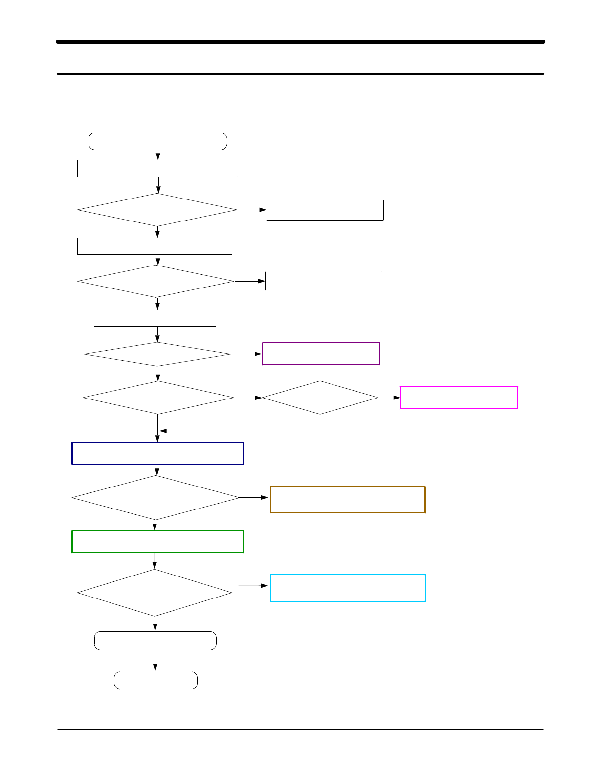
3-1-2. Initial
Initial Failure
Yes
The pin #G11 of UCP100 =
1.8V and
the pin #J12 of UCP100 =
2.8V ?
Yes
No
Flow Chart of Troubleshooting
(if it has some problem, it is to be replaced.)
Check the
UCP100
Is the pin #K9 of UCP100
"Low→High" ?
Yes
There is 32.768kHz wave
forms at the C216 and C217
Yes
Is the pin #A4 of UCP100
is "High"
Yes
The voltage is "High" at the
C112,C114,C115
Yes
LCD display is O.K
No
No
No
No
No
(if it has some problem, it is to be replaced.)
Check the
Check the
Check the
Check the
Check the LCD part
UCP100
UCP200
UCP200
UCP100
Yes
No
Sound is O.K
Yes
END
Check the Audio part
3-5
SAMSUNG Proprietary-Contents may change without notice
This Document can not be used without Samsung's authorization
 Loading...