

Samsung SGH-C260 Service Manual

GSM TELEPHONE
SGH-C260
GSM TELEPHONE
CONTENTS
1. Specification
2. Exploded View and Parts list
3. Chart of Troubleshooting
4. Array course control
5. Block Diagrams
6. PCB Diagrams
7. MAIN Electrical Parts List
8. Reference data
9. Safety Precautions
10. Product Function

Contents
1. Specification
1-1. GSM General Specification .......................................................................................1-1
1-2. GSM TX power class ...............................................................................................1-2
2. Exploded View and Parts list
2-1. Cellular phone Exploded View ..................................................................................2-1
2-2. Cellular phone Parts list ............................................................................................2-2
2-3. Disassembly ...............................................................................................................2-9
2-4. Assembly ..................................................................................................................2-11
3. Chart of Troubleshooting
3-1. Baseband ............................................................................................................3-1
3-1-1. Power ON .....................................................................................................3-1
3-1-2. System Initial ................................................................................................3-5
3-1-3. SIM Part .......................................................................................................3-8
3-1-4. Charging Part .............................................................................................3-10
3-1-5. Microphone Part .........................................................................................3-12
3-1-6. Speaker Part ..............................................................................................3-15
3-1-7. Camera Part ..............................................................................................3-18
3-1-8. LCD .............................................................................................................3-21
3-2. RF ......................................................................................................................3-13
3-2-1. EGSM Rx ...................................................................................................3-23
3-2-2. DCS Rx ......................................................................................................3-24
3-2-3. PCS Rx ......................................................................................................3-25
3-2-4. EGSM Tx ...................................................................................................3-27
3-2-4. DCS & PCS Tx .........................................................................................3-28
3-2-6. BLUETOOTH ..............................................................................................3-30

Contents
4. Array course control
4-1. Downloading Binary Files ......................................................................................4-2
4-2. Pre-requsite for Downloading ................................................................................4-2
4-3. S/W Downloader Program .....................................................................................4-3
5. Block Diagrams
6. PCB Diagrams
7. MAIN Electrical Parts List
8. Reference data
8-1. Reference Abbreviate ..............................................................................................8-1
9. Safety Precautions
9-1. Repair Precaution ......................................................................................................9-1
9-2. ESD(Electrostaically Sensitive Devices) Precaution ................................................9-2
10. Product Function

1. Specification
1-1. GSM General Specification
Freq. Band[MHz]
Uplink/Downlink
ARFCN range
Tx/Rx spacing 45MHz 95MHz
GPRS
Mod. Bit rate/
Bit Period
EDGE
Time Slot Period/Frame Period
GPRS 0.3GMSK 0.3GMSK
Modulation
EDGE 8PSK 8PSK
GSM 900
880~915
925~960
0~124
& 975~1023
270.833Kbps
3.692us
812.5Kbps
3.692us
576.9us
4.615ms
DCS1800
1710~1785
1805~1880
512~885
270.833Kbps
3.692us
812.5Kbps
3.692us
576.9us
4.615ms
MS Power
Power Level
Sensitivity -102dBm -100dBm
TDMA Mux 8 8
Cell Radius 35Km 2Km
GPRS 33dBm~5dBm 30dBm~0dBm
EDGE 27~5dBm 26~0dBm
GPRS 5pcl~19pcl 0pcl~15pcl
EDGE 8~19(class E2) 2~15(class E2)
1-1
Speclflcation
1-2. GSM Tx Power Class
TX Power
control level
5 33±2dBm
6 31±3dBm
7 29±3dBm
8 27±3dBm
9 25±3dBm
10 23±3dBm
11 21±3dBm
12 19±3dBm
13 17±3dBm
GSM900
TX Power
control
level
0 30±2dBm
1 28±3dBm
2 26±3dBm
3 24±3dBm
4 22±3dBm
5 20±3dBm
6 18±3dBm
7 16±3dBm
8 14±3dBm
DCS1800
14 15±3dBm
15 13±3dBm
16 11±5dBm
17 9±5dBm
18 7±5dBm
19 5±5dBm
9 12±4dBm
10 10±4dBm
11 8±4dBm
12 6±4dBm
13 4±4dBm
14 2±5dBm
15 0±5dBm
1-2

2. Exploded View and Parts List
2-1. Cellular phone Exploded View
QFR01
QKP01
QCR12
QMP01
QME01
QSH01
QAN05
QCR12
QAN02
QRF03
QMI01
QMI03
QCR12
QSC05
QFU01
QME03
QLC01
QSP01
QMO01
QHI01
QFL01
QMW02
QRE01
QBA01
QCR06
QBA01
2-1
SAMSUNG Proprietary-Contents may change without notice
This Document can not be used without Samsung's authorization

Main Electrical Parts List
2-2. Cellular phone Parts list
Design LOC Discription SEC CODE
QAN02 INTENNA-SGHC260 GH42-01102A
QAN05 ASSY MEC-INTENNA CONTACT GH75-08168A
QBA00 PMO-CASE BATTERY GH72-36766A
QBA01 INNER BATTERY PACK-750MAH,BLK, GH43-02483A
QCR06 SCREW-MACHINE 6001-001155
QCR12 SCREW-MACHINE 6001-001530
QCR12 SCREW-MACHINE 6001-001530
QCR12 SCREW-MACHINE 6001-001530
QFU01 ASSY CASE-UPPER GH98-03405A
QKP01 ASSY KEYPAD-(XEN/ZR) GH98-03772A
QLC01 LCD-LCD MODULE GH07-01056A
QME01 UNIT-SGHC260 METAL DOME(MAIN) GH59-04084A
QME03 UNIT-SGHC260 CON TO CON GH59-04070A
QMI01 MICROPHONE-ASSY-6.25MM GH30-00177F
QMI03 RMO-MIC HOLDER GH73-05342A
QMO01 MOTOR DC-SGHC260 GH31-00308A
QMP01 PBA MAIN-SGHC260 GH92-03328A
QMW02 PMO-COVER MAIN WINDOW GH72-36767A
QRE01 ASSY CASE-REAR GH98-03406A
QSC05 RMO-COVER FOLDER SCREW GH73-09088A
QSH01 ASSY CASE-SHIELD CAN GH98-03407A
QSP01 SPEAKER 3001-002094
QFR01 ASSY CASE-FRONT GH98-03403A
QRF03 PMO-CASE EAR GH72-36761A
QFL01 ASSY CASE-LOWER GH98-03404A
QHI01 ASSY MEC-HINGE GH75-08452A
2-2
SAMSUNG Proprietary-Contents may change without notice
This Document can not be used without Samsung's authorization

Main Electrical Parts List
Discription SEC CODE
BAG PE 6902-000297
ADAPTOR-SGHC140 DC JACK(EU_B GH44-01597A
LABEL(R)-WATER SOAK GH68-09361A
LABEL(R)-WATER SOAK GH68-09361A
MANUAL USERS-EU PORTUGUESE GH68-13784A
MANUAL USERS-EU ENGLISH GH68-13785A
LABEL(R)-MAIN(EU) GH68-13956A
BOX(P)-UNIT MAIN (EU) GH69-05051A
RMO-RUBBER CSP GH73-08597A
RMO-COVER DUMMY HOLE GH73-08828A
MPR-INSU TAPE GH74-17540A
MPR-VINYL BOHO LCD WIN GH74-20912A
MPR-TAPE MAIN WINDOW GH74-29604A
MPR-TAPE DOPARO LED GH74-30219A
MPR-VINYL BOHO WINDOW JIG GH74-30221A
MPR-SPONGE GH74-30223A
MPR-SPONGE GH74-30638A
MPR-INSU TAPE GH74-30658A
2-3
SAMSUNG Proprietary-Contents may change without notice
This Document can not be used without Samsung's authorization

Main Electrical Parts List
2-3. Disassembly
1
1) Unscrew the REAR.(4 points)
※
caution
1) Be careful not to make scratch and molding da
mage!
2
1) Lift up the lockers in the center of set.
※
caution
1) Be careful not to make scratch and molding
damage!
2) Rem ove the loc ker s in the center by all means.
3
1) Lift up the lockers in the bottom of set.
※
caution
1) Be careful not to make scratch and molding
damage!
4
1) Twist the REAR off the set carefully.
※
caution
1) Be careful not to make scratch and molding
damage!
2-4
SAMSUNG Proprietary-Contents may change without notice
This Document can not be used without Samsung's authorization
Main Electrical Parts List
5
1) Remove the CON TO CON.
※
caution
1) Be careful not to make scratch and molding
damage!
2) Be careful not to damage the CON TO CON .
6
1) Remove the PBA placed at the FRONT.
※
caution
1) Be careful not to make scratch and molding
damage!
2) Be careful not to damage the CON TO CON .
7
1) Unscrew the SHIELD-CAN.(2 points)
※
caution
1) Be careful not to make scratch and molding
damage!
8
1) Remove the KEY-PAD placed at the Front.
※
caution
1) Be careful not to make scratch and molding
damage!
2-5
SAMSUNG Proprietary-Contents may change without notice
This Document can not be used without Samsung's authorization
Main Electrical Parts List
9
1) Remove the tape.
※
caution
1) Be careful not to make scratch and molding
damage!
2) Be careful not to damage the CON TO CON .
10
1)Seperate the FRONT from the FOLDER
assembled.
※
caution
1) Be careful not to make scratch and molding
damage!
2) Be careful not to damage the CON TO CON .
11
1) Remove the screw caps and unscrew the
LOWER. (2points)
※
caution
1) Be careful not to make scratch and molding
damage!
12
1) Lift up the bottom of LOWER removing the
lockers with a tool.
※
caution
1) Be careful not to make scratch and molding
damage!
2-6
SAMSUNG Proprietary-Contents may change without notice
This Document can not be used without Samsung's authorization
Main Electrical Parts List
13
1) Take the rubber out.
※
caution
1) Be careful not to make scratch and molding
damage!
14
1) Remove the LCD F-PCB.
※
caution
1) Be careful not to make scratch and molding
damage!
15
1) Remove the LCD carefully so that the nonwoven
on speaker and motor is not damaged.
※
caution
1) Be careful not to make scratch and molding
damage!
2-7
SAMSUNG Proprietary-Contents may change without notice
This Document can not be used without Samsung's authorization
Main Electrical Parts List
2-4. Assembly
1
1)Put the CON TO CON on the LCD Module
it clicks.
※
caution
1) Be careful not to make scratch and molding
damage!
2) Be careful not to damage the LCD Module.
2
1) Put the LCD Module into place as shown .
2) Put the speaker and motor into place.
※
caution
1) Be careful not to make scratch and molding
damage!
3
1) Place the MIC as the picture below
※
caution
1) Be careful not to make scratch and molding
damage! TORQE (1.0 ± 0.1 Kgf·Cm)
4
1) Put the MIC COVER and CREW
2) Attach KEYPAD
3) Press the KEYPAD not to be detached
※
caution
1) Be careful not to make scratch and molding
damage!
2-8
SAMSUNG Proprietary-Contents may change without notice
This Document can not be used without Samsung's authorization

Main Electrical Parts List
5
1) Fasten 2 screws.
2) Put the screw caps on the FOLDER.
※
caution
1) Be careful not to make scratch and molding
damage!
TORQE (1.0 ± 0.1 Kgf·Cm)
6
1) Put one side of the FOLDER into the FRONT
firstly,do the other side pressing the hinge.
※
caution
1)Be careful not to damage the F-PCB.
7 8
1) Put a tape on.
※
caution
1) Be careful not to damage the wire on the
speaker due to PBA.
1) Place the KEY-PAD into the FRONT.
※
caution
1) Be careful not to make scratch and molding
damage!
2-9
SAMSUNG Proprietary-Contents may change without notice
This Document can not be used without Samsung's authorization
Main Electrical Parts List
9
1) As shown,put the CON TO CON on PBA.
※
caution
1) Be careful not to make scratch and molding
damage!
2) Press the CON TO CON down firmly.
10
1) Press the bottom of REAR down until it
clicks.
※
caution
1) Be careful not to make scratch and molding
damage!
2) Be careful not to damage the locker.
11 12
1) Press the both sides of the REAR using
the lockers.
※
caution
1) Be careful not to make scratch and molding
damage!
2) Be careful not to damage the locker.
1) Press the top down until the lockers click
※
1) Be careful not to make scratch and molding
2) Be careful not to damage the locker.
grasping with your fingers carefully.
caution
damage!
2-10
SAMSUNG Proprietary-Contents may change without notice
This Document can not be used without Samsung's authorization

Flow Chart of Troubleshooting
3.
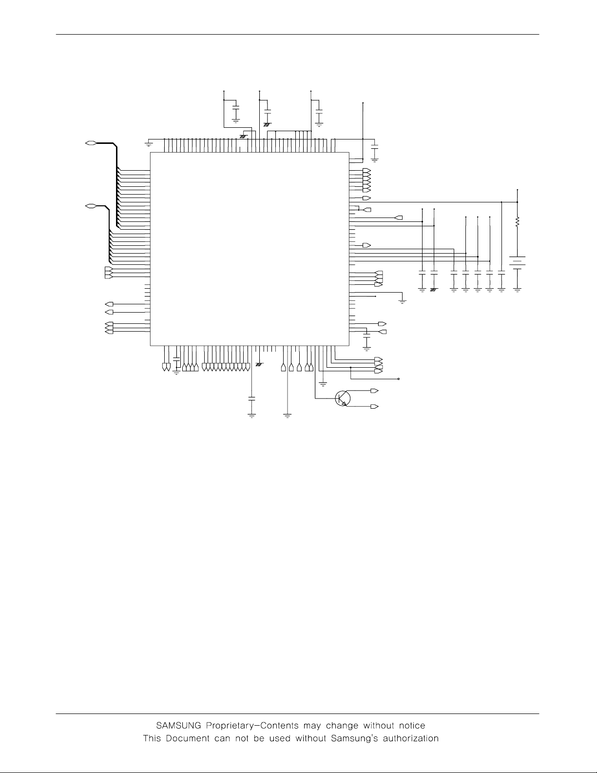
3-1. Baseband
3-1-1. Power ON
'Power ON' does not work
check the current
consumption
>= 100mA
Yes
Check the Voltage
of the Battery
>= 3.3V
Yes
Check the pin
3
C152,C153,C155 of
UCP107 is >= 2.8V
>=2.8V
Yes
Check the clock signal
atpin#3ofOSC101
Freq=26Mhz
Vrms >=300mV
No
No
No
No
Download again
Charge the battery
Check "Power
On"
key?
Check the clock generation
circuit OSC101
Yes
No
Check"Power On"Key
1
check UCD107 and C153
2
Yes
Check the Initial Operation
Yes
END
3-1

Flow Chart of Troubleshooting
C132
VRF_2.9V
C183
4
GND2
HOT
1
3
HOT
GND1
2
OSC101
DPCS_PAM_IN
GSM_PAM_IN
VBAT
AFC
C147
C145
C151
R195
R102
R143
C146
C125
25V
C119 25V
C123
SERCLK
SERDAT
C124
SERLE
RTXIN
RTXIP
VCCD_2.9V
C150
C121
VLDO2
6
1
VLDO1
5
1
VBAT
4
1
VDD
3
1
VCC_TXVCO
2
1
TXOP_HI
1
1
TXOP_LO
0
1
VLDO3
9
RTXQN26M_OUT
RTXQP
3
7
8
1
1
F
C
B
E
F
N
R
I
A
_
F
V
C
E
C
R
V
K
N
L
E
C
C
S
S
N
7
8
1
9
0
2
1
2
P
N
B
I
O
Q
F
_
E
F
R
E
R
UCD101
I
B
A
B
_
T
C
A
C
D
B
V
I
S
5
6
4
4
2
2
2
2
Q
Q
B
B
_
RX1900B
C
C
V
RX1900
RX1800B
RX1800
RX900B
RX850B
E
F
_
C
C
V
I
3
2
1
RX900
RX850
GND
C
N
5
3
5
2
6
2
7
2
8
2
9
2
0
3
1
3
2
3
3
3
C
N
4
3
C184
DCS_LNA_IN_P
DCS_LNA_IN_N
GSM_LNA_IN_P
GSM_LNA_IN_N
C189
3-2
Flow Chart of Troubleshooting
DSP_DB(0:15)
DSP_AB(0:8)
FLASH_RESET
DSP_IO
DSP_RWN
VMOD_EN
TX_EN
SERLE
SERDAT
SERCLK
DSP_DB(15)
DSP_DB(14)
DSP_DB(13)
DSP_DB(12)
DSP_DB(11)
DSP_DB(10)
DSP_DB(9)
DSP_DB(8)
DSP_DB(7)
DSP_DB(6)
DSP_DB(5)
DSP_DB(4)
DSP_DB(3)
DSP_DB(2)
DSP_DB(1)
DSP_DB(0)
DSP_AB(8)
DSP_AB(7)
DSP_AB(6)
DSP_AB(5)
DSP_AB(4)
DSP_AB(3)
DSP_AB(2)
DSP_AB(1)
DSP_AB(0)
D2
D3
E3
E2
F3
F2
F1
F4
G4
G3
H5
J6
J5
K3
K2
K1
K5
K7
M1
M2
N2
N1
L5
P1
K6
L3
L2
R3
E6
C5
F5
E5
A4
G6
B3
A3
B1
A2
C1
C2
2
DB15
DB14
DB13
DB12
DB11
DB10
DB9
DB8
DB7
DB6
DB5
DB4
DB3
DB2
DB1
DB0
AB8
AB7
AB6
AB5
AB4
AB3
AB2
AB1
AB0
I|O
RWN
RESETN_CSP
NC4
OCTL1
OCTL2
NC
OCTL4
OCTL5
OCTL6
OCTL7
SERLE1
SERLE2
SERDA
SERCK
C
F
A
9
D
VCCD_2.9V
VCCA_2.9V
C153
C152
0
0
1
1
J
K
1
7
6
6
5
1
1
C
C
S
S
N
N
D
D
N
N
G
G
0
1
6
9
8
7
9
8
7
H
G
J
J
J
H
H
H
9
8
5
4
3
2
1
0
1
1
1
1
1
1
S
S
S
S
S
S
S
S
D
D
D
D
D
D
D
D
N
N
N
N
N
N
N
N
G
G
G
G
G
G
G
G
3
0
9
8
7
1
1
9
8
7
G
G
G
F
F
F
D
F
7
6
5
4
3
2
8
1
S
S
S
S
S
S
S
C
D
D
D
D
D
D
D
N
N
N
N
N
N
N
N
G
G
G
G
G
G
G
0
3
1
1
4
4
6
1
6
1
F
C
M
L
B
A
P
L
L
V
V
B
D
B
T
T
D
D
D
D
D
C
C
N
D
N
N
D
O
O
V
V
G
G
G
_
_
D
D
D
N
V
G
UCD107
N
P
N
P
T
P
A
A
X
T
R
R
7
6
5
E
B
B
C
C
C180
F
P
A
A
100NF
V
10V
O
O
O
X
X
X
X
A
A
A
R
R
R
R
1
2
7
2
6
7
6
1
1
1
C
D
D
C
P
N
R
P
P
P
P
N
N
N
I
I
A
B
A
Q
Q
X
X
T
T
T
X
X
T
T
U
T
U
U
T
R
R
R
O
R
O
O
A
A
A
P
N
P
N
P
2
1
N
P
B
A
A
F
F
I
I
Q
Q
T
T
T
E
E
X
X
X
X
U
U
U
R
R
T
T
T
T
T
N
T
T
P
N
U
U
B
P
N
U
T
N
N
I
O
I
U
C
C
C
I
I
I
O
A
M
M
M
2
5
4
4
1
1
1
1
P
N
N
M
P
P
N
N
T
N
N
B
I
I
U
T
C
C
I
I
O
U
M
C
M
O
I
A
M
N
P
M
U
O
C
I
M
5
1
P
N
T
U
O
C
I
M
K
N
N
N
I
I
X
X
U
U
A
A
4
5
1
1
L
M
P
N
N
N
I
I
X
X
U
U
A
A
I
O
O
G
G
C
C
R
D
X
X
I
I
I
E
E
V
U
U
A
A
A
R
R
X
A
A
D
D
D
V
V
V
3
3
4
4
6
4
3
3
1
1
1
1
1
L
P
R
L
K
R
R
M
P
N
T
T
U
U
O
O
X
X
U
U
A
A
C182
VCCD_2.9V
3
1
B
Q
D
N
G
P
E
E
K
_
Q
R
R
T
W
N
P
I
0
1
L
0
1
C
7
5
6
D
D
D
VDD34
D
V
V
VDD12
UP_CLK
UP_RST
SIM_IO
SIM_RST
SIM_CLK
LED2_DRV
LED1_DRV
RING_DRV
VIB_DRV
VLDO_7
VLDO_6
VL5S_B
VL5S_A
VLDO_5
VL4S_B
VL4S_A
VLDO_4
VLDO_3
VLDO_2
VLDO_1
CSN_PSC
SCLK_PSC
SDO_PSC
SDI_PSC
CH_BDRV
CH_ISEN
CH_RES
RTC_ALMN
D
V
S
R
9
L
1
UP_IO
VRTC
VACC
VEXT
VBAT
VREF
CREF
Q103
VBAT
C162
C11
J13
N9
SIMCLK
R10
SIMRST
P10
SIMDATA
J11
SIM_IO
K11
SIM_RST
K14
SIM_CLK
K12
VSIM
NC3
NC9
VSIM
H11
G12
G13
KEY_BL1
F13
F15
C12
A14
C9
D10
B10
B11
A12
BAND_SEL1
B12
A13
J12
G11
F14
K8
L8
N7
M7
E14
E13
E11
F12
D14
D15
E10
A10
E9
H10
VBAT
UP_CS
UP_SCLK
UP_SDO
UP_SDI
VREF
RTCALARM
VCCB_2.9V
VIB_DRV
C168
VCCA_2.9V
C170
VRF_2.9V
C171
VCCD_2.9V
C172
VCCD_1.8V
C173
C174
VRTC_3V
C175
R157
1
M300
2
C179
VIB_EN
INTRQ
PWR_KEEP
RST
TP2
KEY_COL(2)
3
2
KEY_ROW(0)
C155
5
1
5
1
4
2
6
N
K
G
R
P
1
2
3
4
D
S
S
S
S
D
S
S
S
S
D
V
V
V
V
V
K
Q
L
A
C
O
N
_
D
I
E
C
C
A
T
O
M
D
R
X
6
6
4
1
R
N
D
M
K
2
3
_
K
L
C
5
1
3
1
1
5
6
8
1
4
3
K
B
F
E
N
J
N
J
M
2
1
2
1
3
1
2
R
C
C
D
D
D
O
O
U
I
I
S
S
D
D
D
_
_
C
P
P
V
V
V
H
D
D
_
_
_
D
D
D
D
D
V
V
N
N
N
G
G
G
N
F
2
1
U
O
W
W
B
_
S
S
_
2
T
_
_
R
1
D
E
T
R
R
7
V
S
W
N
I
S
E
C
W
W
S
P
P
P
D
R
R
N
4
5
9
7
0
3
9
5
1
1
1
L
P
P
K
M
C
C
N
T
N
N
C
N
O
O
M
I
_
_
_
_
R
P
G
M
I
S
3
J
W
1
D
P
K
L
C
3-3
 Loading...