

Samsung SGH-C210 Service Manual
GSM TELEPHONE
SGH-C210
GSM TELEPHONE
CONTENTS
1. Specification
2. Circuit Description
3. Exploded Views and Parts List
4. Electrical Parts List
5. Block Diagrams
6. PCB Diagrams
7. Flow Chart of Troubleshooting

1. Specification
1-1. GSM General Specification
EGSM 900
Phase 2
Freq. Band[MHz]
Uplink/Downlink
ARFCN range 0~124 & 975~1023 512~885 512~810
Tx/Rx spacing 45MHz 95MHz 80MHz
Mod. Bit rate/
Bit Period
Time Slot
Period/Frame Period
Modulation 0.3GMSK 0.3GMSK 0.3GMSK
MS Power 33dBm~5dBm 30dBm~0dBm 30dBm~0dBm
880~915
925~960
270.833kbps
3.692us
576.9us
4.615ms
DCS 1800
Phase 1
1710~1785
1805~1880
270.833kbps
3.692us
576.9us
4.615ms
PCS 1900
Phase 1
1850~1910
1930~1960
270.833kbps
4.615ms
3.692us
576.9us
Power Class 5pcl ~ 19pcl 0pcl ~ 15pcl 0pcl ~ 15pcl
Sensitivity -102dBm -100dBm -1 00dBm
TDMA Mux 8 8 8
Cell Radius 35Km 2Km 2Km
Operating
Temperature
-20°C ~ +50°C
1-1
SAMSUNG Proprietary-Contents may change without notice
This Document can not be used without Samsung's authorization

2. Circuit Description
2-1. SGH-C210 RF Circuit Description
2-1-1. RX PART
—
ASM(F101)→Switching Tx, Rx path for GSM900, DCS1800 and PCS1900 by logic controlling.
—
ASM Control Logic Truth Table
VC1 VC2 VC3
EGSM TX H L L
DCS/PCS TX L H L
PCS_RX L L H
—
Saw FILTER
To convert Electromagnetic Field Wave to Acoustic Wave and then pass the specific frequency band.
- GSM FILTER (F100)→For filtering the frequency band between 925 and 960 MHz.
- DCS FILTER (F100)→For filtering the frequency band between 1805 and 1880 MHz
- PCS FILTER (F102)→For filtering the frequency band between 1930 and 1990 MHz.
—
Crystal (X101)
To generate the 26MHz reference clock to drive the logic and RF.
After additional process, the reference clock applies to the U801 Rx IQ demodulator and Tx IQ modulator.
The oscillator for RX IQ demodulator and Tx modulator are controlled by serial data to select channel and use fast lock
mode for GPRS high class operation.
—
Si4210 (U102)
The receive section integrates four differential-input low noise amplifiers LNAs supporting the GSM850, EGSM900,
DCS1800 and PCS1900 bands. The LNA inputs are matched to the 150 ohm balanced-output SAW filters through externa
LC matching network.
A quadrature Image-reject mixer downconverts the RF signal to a 200 KHz intermediate frequency(IF). The mixer output is
amplified with an analog programmable gain amplifier(PGA) that is controlled with the AGAIN. The quadrature IF
is digitized with high resolution analog-to-digital converts (ADC).
The ADC output is downconverted to baseband with a digital quadrature LO signal. Digital decimation and FIR filters
perform digital filtering and remove ADC quantization noise, blockers and reference interferers.
After filtering, the digital output is scaled with a digital PGA, which is controlled with the DGAIN. DACs drive a
differential I and Q analog signal onto the BIP, BIN, BQP and BQN pins to interface to standard analog-input baseband
ICs.
? ?
2-1
SAMSUNG Proprietary-Contents may change without notice
This Document can not be used without Samsung's authorization

Circuit Description
2-1-2. TX PART
Baseband IQ signal fed into offset PLL, this function is included inside of U801 chip. The transmit section of U801
consist of an I/Q baseband upconverter, an offset phase-locked loop (OPLL) and two 50 ohm output buffers that can drive
an external Power Amplifier(PA). Si4210 chip generates modulator signal which power level is about 1.5dBm and fed into
Power Amplifier(U900). The PA output power and power ramping are well controlled by Auto Power Control circuit.
We use offset PLL below.
GSM -35dBc
DCS -35dBc
PCS -35dBc
GSM -66dBc
DCS -65dBc
PCS -66dBc
GSM -75dBc
DCS -68dBc
PCS -75dBc
Modulation Spectrum
200kHz offset
30 kHz bandwidth
400kHz offset
30 kHz bandwidth
600kHz ~ 1.8MHz offset
30 kHz bandwidth
2-2. Baseband Circuit description of SGH-C210
2-2-1. CSP2200B1
—
Power Management
Seven low-dropout regulators designed specifically for GSM applications power the terminal and help ensure optimal
system performance and long battery life. A programmable LDO provides support for 1.8V, 3.0V SIMs, while a selfresetting, electronically fused switch supplies power to external accessories. Ancillary support functions, such as two LED
drivers and two call-alert drivers, aid in reducing both board area and sy stem complexity. A four-wire serial interface
unit(SIU) provides access to control and configuration registers. This interface gives a microprocessor full control of the
CSP2200B1 and enables system designers to maximize both standby and talk times. Error reporting is provided via an
interrupt signal and status register. Supervisory functions. including a reset generator, an input voltage monitor, and a
thermal monitor, support reliable system design. These functions work together to ensure proper system behavior during
start-up or in the event of a fault condition(low microprocessor voltage, insufficient battery energy, or excessive die
temperature).
—
Battery Charge Management
A battery charge management block, incorporating an internal PMOS switch, and an 8-bit ADC, provides fast, efficient
charging of single-cell Li-Ion battery. Used in conjunction with a current-limited voltage source, this block safely
conditions near-dead cells and provides the option of having fast-charge and top-off controlled internally or by the system's
microprocessor.
2-2
SAMSUNG Proprietary-Contents may change without notice
This Document can not be used without Samsung's authorization

Circuit Description
—
Backlight LED Driver
The backlight LED driver is a low-side, programmable current source designed to control the brightness of the keyboard
illumination. LED1_DRV is controlled via LED1_[0:2] and can be programmed to sink from 15mA to 60mA in 7.5mA
steps. LED2_DRV is controlled via LED2_[0:2] and can be programmed to sink from 5mA to 40mA in 5mA steps.
Both LED drivers are capable of sinking their maximum output current at a worst-case maximum output voltage of 0.6V.
For efficient use, the LEDs is connected between the battery and the LED_DRV output.
—
Vibrator Motor Driver
The vibrator motor driver is a independent voltage regulator to drive a small dc motor that silently alerts the user of an
incoming call. The driver is a 3.3V constant source while sinking up to 140mA and controlled by enable signal of main
chip. For efficient use and safety, the vibrator motor should be connected between the regulator output and the ground.
2-2-2. Connector
—
JTAG Connector
Trident has two JTAG ports which are for ARM core and DSP core(DSP16000). So this system has two port connector
for these ports. Pins' initials for ARM core are 'CP_' and pins' initials for DSP core are 'DSP_'.
CP_TDI and DSP_TDI signal are used for input of data. CP_TDO and DSP_TDO signals are used for the output of the
data. CP_TCK and DSP_TCK signals are used for clock because JTAG communication is a synchronous. CP_TMS and
DSP_TMS signals are test mode signals. The difference between these is the RESET_INT signal which is for ARM core
RESET.
—
Keypad connector
This is consisted of key interface pins in the trident, KEY_ROW[0~4] and KEY_COL[0~4]. These signals compose the
matrix. Result of matrix informs the key status to key interface in the trident. Some pins are connected to varistor for
ESD protection. And power on/off key is seperated from the matrix.
So power on/off signal is connected with CSP2200 to enable CSP2200.
Nine key LED use the +VBATT supply voltage. These are connected to BACKLIGHT signal in the CSP2200.
This signal enables LEDs with current control.
—
EMI Filtering
This system uses the EMI Filter to reduce noise from LCD part. Some control signals are connected to LCD without EMI
filtering.
2-3
SAMSUNG Proprietary-Contents may change without notice
This Document can not be used without Samsung's authorization

Circuit Description
2-2-3. IF connetor
It is 24-pin connector, and separated into two parts. One is a power supply part for main system. And the other is
designed to use SDS, DEBUG, DLC-DETECT, JIG_ON, VEXT, VTEST, VF, and GND. They connected to power supply
IC, microprocessor and signal processor IC.
2-2-4. Audio
AOUTAP, AOUTAN from CSP2200 is connected to the speaker via analog switch. AOUTBP and AOUTBN are connected
to the ear-mic speaker via ear-jack. MICIN and MICOUT are connected to the main MIC. And AUXIN and AUXOUT
are connected to the Ear-mic.
YMU762MA3 is a LSI for portable telephone that is capable of playing high quality music by utilizing FM synthesizer
and ADPCM decorder that are included in this device.
As a synthesis, YMU762MA3 is equipped 16 voices with different tones. Since the device is capable of simultaneously
generating up to synchronous with the play of the FM synthesizer, various sampled voices can be used as sound effects.
Since the play data of YMU762MA3 are interpreted at anytime through FIFO, the length of the data(playing period) is not
limited, so the device can flexibly support application such as incoming call melody music distribution service. The
hardware sequencer built in this device allows playing of the complex music without giving excessive load to the CPU of
the portable telephones. Moreover, the registers of the FM synthesizer can be operated directly for real time sound
generation, allowing, for example, utilization of various sound effects when using the game software installed in the
portable telephone.
YMU762 includes a speaker amplifier with high ripple removal rate whose maximum output is 550mW (SPVDD=3.6V).
The device is also equipped with conventional function including a vibartor and a circuit for controlling LEDs synchornous
with music.
For the headphone, it is provided with a stereophonic output terminal.
For the purpose of enabling YMU762MA3 to demonstrate its full capabilities, Yamaha purpose to use "SMAF:Synthetic
music Mobile Application Format" as a data distribution format that is compatible with multimedia.
Since the SMAF takes a structure that sets importance on the synchronization between sound and images, various contents
can be written into it including incoming call melody with words that can be used for training karaoke, and commercial
channel that combines texts, images and sounds, and others. The hardware sequencer of YMU762MA3 directly interprets
and plays blocks relevant to sy nthesis (playing music and reproducing ADPCM with FM synthesizer) that are included in
data distributed in SMAF.
2-4
SAMSUNG Proprietary-Contents may change without notice
This Document can not be used without Samsung's authorization

Circuit Description
2-2-5. Memory
This system uses SHARP's memory, LRS18B0.
It is consisted of 256M bits flash memory and 64M bits SCRAM. It has 16 bit data line, D[0~15] which is connected to
trident, LCD or CSP2200. It has 23 bit address lines, A[1~23]. They are also connected. CP_CSROMEN signal, chip
select signal in the trident, enable flash memories. They use supply voltages, VCCD and VCC_1.8A.
During wrting process, CP_WEN is low and it enables writing process to flash memory and SCRAM. During reading
process, CP_OEN is low and it output information which is located at the address from the trident in the flash memory or
SCRAM to data lines. Each chip select signals in the trident select flash memory or SCRAM. Reading or writing
procedure is processed after CP_WEN or CP_OEN is enabled. Memories use FLASH_RESET, which is buffered signal of
RESET from CSP2200, for ESD protection. A[0] signal enables lower byte of SCRAM and UPPER_BYTE signal enables
higher byte of SCRAM.
2-2-6. Trident
Trident is consisted of ARM core and DSP core. It has 20K*16bits RAM 144K*16bits ROM in the DSP. It has
4K*32bits ROM and 2K*32bits RAM in the ARM core. DSP is consisted of timer, one bit input/output unit(BIO), JTAG,
EMI and HDS(Hardware Development System). ARM core is consisted of EMI, PIC(Programmable Interrupt Controller),
reset/power/clock unit, DMA controller, TIC(Test Interface Controller), peripheral bridge, PPI, SSI(Synchronous Serial
Interface), ACCs(Asynchronous communications controllers), timer, ADC, RTC(Real-Time Clock) and keyboard interface.
DSP_AB[0~8], address lines of DSP core and DSP_DB[0~15], data lines of DSP core are connected to CSP2200. A[0~20],
address lines of ARM core and D[0~15], data lines of ARM core are connected to memory, LCD and YMU762.
ICP(Interprocessor Communication Port) controls the communication between ARM core and DSP core.
CSROMEN, CSRAMEN and CS1N to CS4N in the ARM core are connected to each memory. WEN and OEN control the
process of memory. External IRQ(Interrupt ReQuest) signals from each units, such as, YMU, Ear-jack, Ear-mic and
CSP1093, need the compatible process.
Some PPI pins has many special functions. CP_KB[0~9] receive the status from key FPCB and are used for the
communications using data link cable(DEBUG_DTR/RTS/TXD/RXD/CTS/DSR).
And UP_CS/SCLK/SDI, control signals for CSP2200 are outputted through PPI pins. It has signal port for
charging(CHG_DET), SIM_RESET and FLIP_SNS with which we knows open.closed status of folder. It has JTAG control
pins(TDI/TDO/TCK) for ARM core and DSP core. It recieves 13MHz clock in CKI pin from external TCXO and receives
32.768KHz clock from X1RTC. ADC(Analog to Digital Convertor) part receives the status of temperature, battery type and
battery voltage. And control signals(DSP_INT, DSP_IO and DSP_RWN) for DSP core are used. It enables main LCD with
DSP IP pins.
2-5
SAMSUNG Proprietary-Contents may change without notice
This Document can not be used without Samsung's authorization

Circuit Description
2-2-7. CSP2200
CSP2200 is integrated the timing and control functions for GSM 2+ mobile application with the ADC and DAC functions,
and power management block. The CSP2200 interfaces to the trident, via a 16-bit parallel interface. It serves as the
interface that connects a DSP to the RF circuitry in a GSM 2+ mobile telephone. DSP can load 148 bits of burst data
into CSP2200’s internal register, and program CSP2200’s event timing and control register with the exact time to send the
burst. When the timing portion of the event timing and control register matches the internal quarter-bit counter and internal
frame counter, the 148 bits in the internal register are GMSK modulated according to GSM 2+ standards. The resulting
phase information is translated into I and Q differential output voltages that can be connected directly to an RF modulator
at the TXOP and TXON pins. The DSP is notified when the transmission is completed. For receiving baseband data, a
DSP can program CSP2200’s event timing and control register with the exact time to start receiving I and Q samples
through TXIP and TXIN pins. When that time is reached, the control portion of the event timing and control register will
start the baseband receive section converting I and Q sample pairs. The samples are stored in a double-buffered register
until the register contains 32 sample pairs. CSP2200 then notifies the DSP which has sample time to read the information
out before the next 32 sample pairs are stored. The voice band ADC converter issues an interrupt to the DSP whenever it
finishes converting a 16-bit PCM word. The DSP then reads the new input sample and simultaneously loads the voice
band output DAC converter with a new PCM output word. The voice band output can be connected directly to a speaker
via AOUTAN and AOUTAP pins and be connected to a Ear-mic speaker via AOUTBN and AOUTBP pins.
There are 7 LDOs which are power sources of microprocessor, LCD, etc. These 7 LDOs output are programmable.
2-6
SAMSUNG Proprietary-Contents may change without notice
This Document can not be used without Samsung's authorization
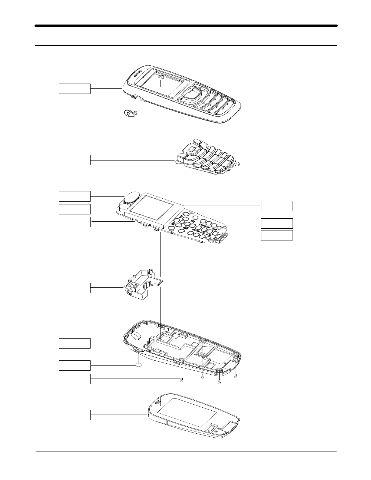
3. Exploded View and Parts List
3-1. Exploded View
QFR01
QKP01
QSP01
QMO01
QLC01
QMP01
QAN01
QRE01
QRF01
QCR31
QME01
QMI01
QBA01
3-1
SAMSUNG Proprietary-Contents may change without notice
This Document can not be used without Samsung's authorization
Exploded view and Part List
3-2. Parts List
Location
Description SEC CODE Remark
NO.
QFR01 FRONT COVER GH75-06802A
QKP01 KEYPAD GH75-06998A
QSP01 SPEAKER 3001-001760
QMO01 MOTOR DC GH31-00163A
QMP01 PBA MAIN GH92-02142A
QLC01 LCD GH07-00701A
QME01 UNIT METAL DOME GH59-02090A
QMI01 MICROPHONE ASSY GH30-00186A
QAN01 INTENNA GH42-00552A
QRE01 REAR COVER GH75-06804A
QRF01 TAPE PC RF GH74-14175A
QCR31 SCREW 6001-001795
QBA01 BATTERY GH43-01817A
3-2
SAMSUNG Proprietary-Contents may change without notice
This Document can not be used without Samsung's authorization

Exploded view and Part List
Description SEC CODE
BAG PE;LDPE,T0.05,W80,L180,TRP,-,- 6902-000634
ADAPTOR-TAD;TAD137ESE,SGH-P100,-,110 GH44-00482A
LABEL(P)-WATER SOAK;SCH-X110,NORGE,1 GH68-02026A
MANUAL-SFC;SGH-S200,SAMSUNG,RUSSIAN, GH68-04336A
LABEL(R)-MAIN( SER);SGH-C210,SER,POL GH68-06983B
MANUAL-USE;SGH-C210,SER,RUSSIAN,ROMA GH68-07137A
CUSHION-CASE(1-2);SGH-C210,PULP,T0.8 GH69-02937A
MPR-ESD TAPE;SGH-C200,3M 851,7X5,-,- GH74-08853A
MPR-BOHO VINYL M/WIN;SGH-C200,STA EL GH74-09824B
MPR-MAIN WINDOW BOHO;SGH-C200,ST 555 GH74-11636A
3-3
SAMSUNG Proprietary-Contents may change without notice
This Document can not be used without Samsung's authorization

Exploded view and Part List
3-3. Test Jig (GH80-00865A)
3-3-1. RF Test Cable
(GH39-00283A)
3-3-4. Power Supply Cable
3-3-2. Test Cable
(GH39-00127A)
3-3-5. DATA CABLE
(GH39-00143B)
3-3-3. Serial Cable
3-3-6. TA
(GH44-00184A)
3-4
SAMSUNG Proprietary-Contents may change without notice
This Document can not be used without Samsung's authorization
 Loading...