

Samsung SGH-B520 Troubleshoot
10. Flow Chart of Troubleshooting
10-1.Baseband
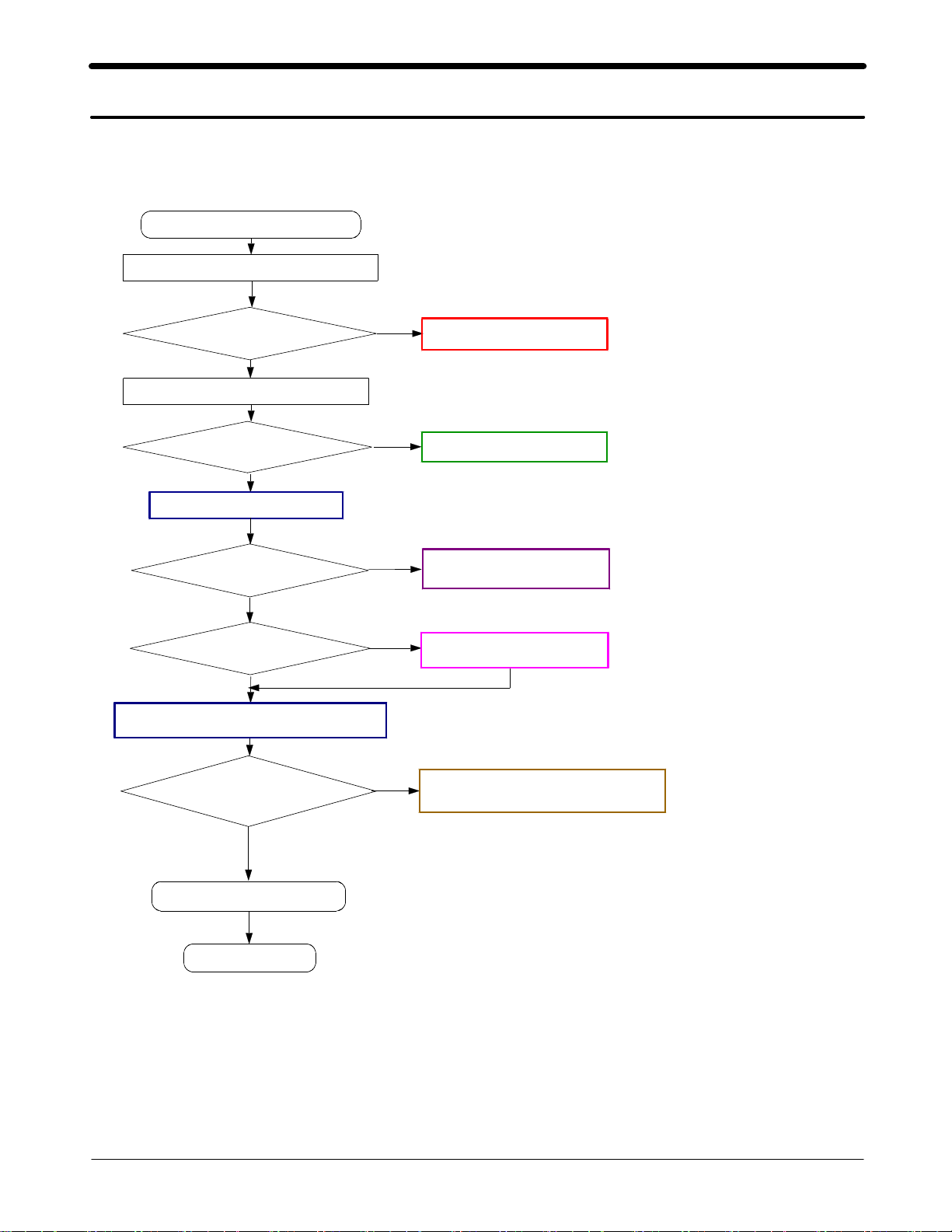
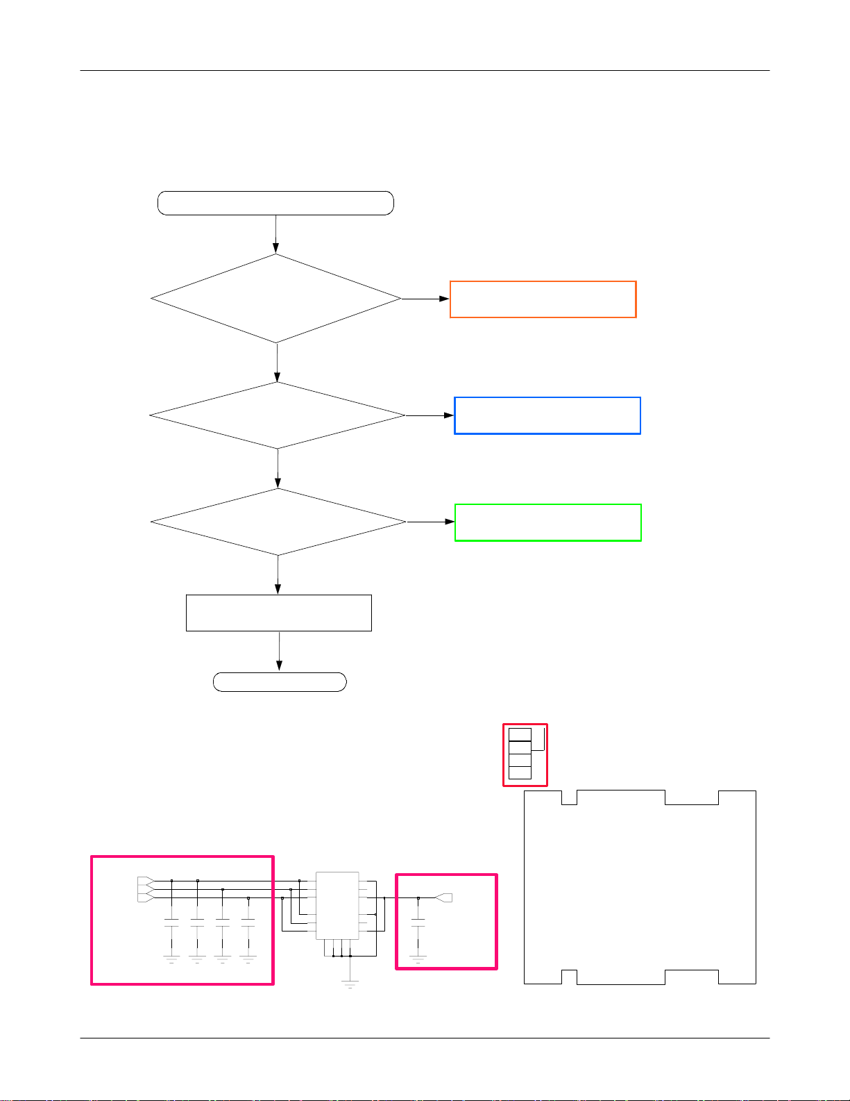
10-1-1. Power ON
'Power On' does not work
Check the current consumption
Yes
Current consumption
>= 100mA
Yes
Check the Vbat Voltage
Voltage >=3.3V
Yes
Check the pin of UCP300
Pin#A6 : 1.8V
Pin#D6 : 2.9V
Yes
Pin#M7 : 2.9V
Pin#L8,#P4 : 1.8V
Yes
Check the clock signal at Pin#12(C118) of RFT100
Yes
No
No
No
No
Download again
Charge the Battery
Check UCP300
C332 and C331
Check UCP300
C300,C301,C303
Freq = 26MHz
Vrms >=300mV
Vpp≒900mV
Yes
Check the initial operation
END
SAMSUNG Proprietary-Contents may change without notice
This Document can not be used without Samsung's authorization
No
Check the clock generation circuit
(related to OSC100, Pin#9, Pin#10)
10-1
Flow Chart of Troubleshooting
S
D
N
G
2
1
_
_
L
L
P13
USB_CARKIT_D_N
P12
USB_CARKIT_D_P
C10
USB_CHRG
A6
VLDO_1
D6
VLDO_2
E14
VLDO_AUD
F12
VLDO_AUX1
D14
VLDO_AUX2
C15
VLDO_COREA
B15
VLDO_COREA_S
C12
VLDO_COREB
D13
9
0
2
3
3
3
C
C
2
1
3
3
3
3
C
C
VLDO_COREC
L300
C
C
UCP300
3
1
9
C332
3
2
1
C331
C311
C313
S
S
Q
B
D
D
D
D
S
S
S
N
N
N
S
S
S
V
6
K
G
V
G
V
G
1
8
9
1
4
1
F
K
K
K
N
S
S
S
D
D
D
D
D
N
N
N
N
N
G
G
G
G
G
0
1
E
0
7
6
9
8
1
F
F
F
F
F
R331
S
S
D
D
N
N
G
G
C340
1
6
1
G
F
C306
TH300
R303
C305
C320
R306
C308
C307
C323
C309
C
3
0
0
O
S
0
0
3
P
C
U
C
C
3
3
C315
C345C346
0
1
0
6
C
3
1
C301
4
R331
C340
RTX_I_P
RTX_I_N
RTX_Q_P
RTX_Q_N
CLK26M_BT
CLK26M_DBB
C304
SBCK
SBDT
SBLE
VCCD_1.8VVCCD_2.9V VCCA_2.8V
C
C
3
3
2
2
6
5
C
C
3
3
2
2
7
8
C300
A4
ADC_AUX1
B4
ADC_AUX2
B3
ADC_AUX3
A2
ADC_AUX4
B1
ADC_AUX5
C1
ADC_AUX6
C2
C301
5
4
2
7
2
1
1
1
1
K
N
M
D
C
N
C
A
B
D
D
D
1
B
D
D
D
D
1
D
V
V
V
D
D
D
V
V
D
V
UCP300
C112
C118
C302
0
5
1
5
4
8
1
1
1
L
P
K
L
P
N
L
V
R
D
O
O
I
I
T
D
K
D
_
_
C
D
P
D
D
D
O
V
S
V
D
D
A
D
V
V
_
D
D
V
D
V
C
N
1
A
2
AX
3
B
4
BX
5
VDD1
6
FSYS3
7
FSYS2
8
VDD2
9
XO
10
XOX
C303
C309
5
6
1
2
F
C
D
D
X
X
D
D
E
N
N
G
RFT100
D
N
G
1
1
N
D
R
G
V
R
1
3
S
D
K
Y
L
D
S
C
V
F
3
2
1
1
26
T
T
D
VDD4
V
25
RX1X
24
RX1
23
RX2X
22
RX2
21
GND
20
RX3X
19
RX3
18
RX4X
17
RX4
A
N
D
E
4
6
5
1
1
1
VRF_1.5V
GSM
GSM
DCS_
DCS_
C119
C
C
4
3
1
2
2
9
C
C
C
3
4
3
2
1
3
4
4
0
C
1
1
2
OSC100
R409R410
C
4
1
1
C345C346
R
1
0
1
C101
R
R
4
4
0
0
1
3
C
4
0
7
C402
C
R
4
4
0
0
3
6
0
0
3
P
C
U
C315
C
3
1
4
R
1
2
2
R413
C425
C
R
C
4
0
4
2
0
9
C
4
2
4
C318
C
C
3
3
0
1
0
6
C301
C
1
0
2
C317
C302
C303
R
C
4
4
4
2
1
2
7
7
2
C
C
R
4
4
4
2
2
1
4
6
9
R238
VR200
R251
R267
R
F
T
1
0
0
C120
C116
C115
C113
L
1
0
6
L
1
0
5
C11 8 C119
10-2
SAMSUNG Proprietary-Contents may change without notice
This Document can not be used without Samsung's authorization
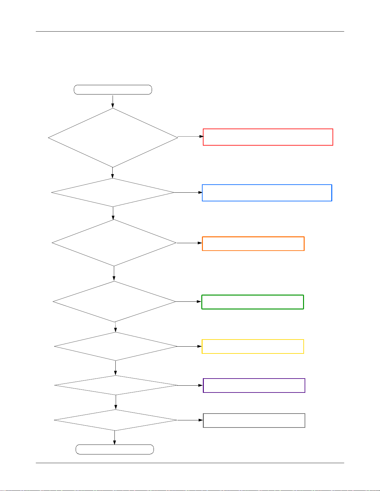
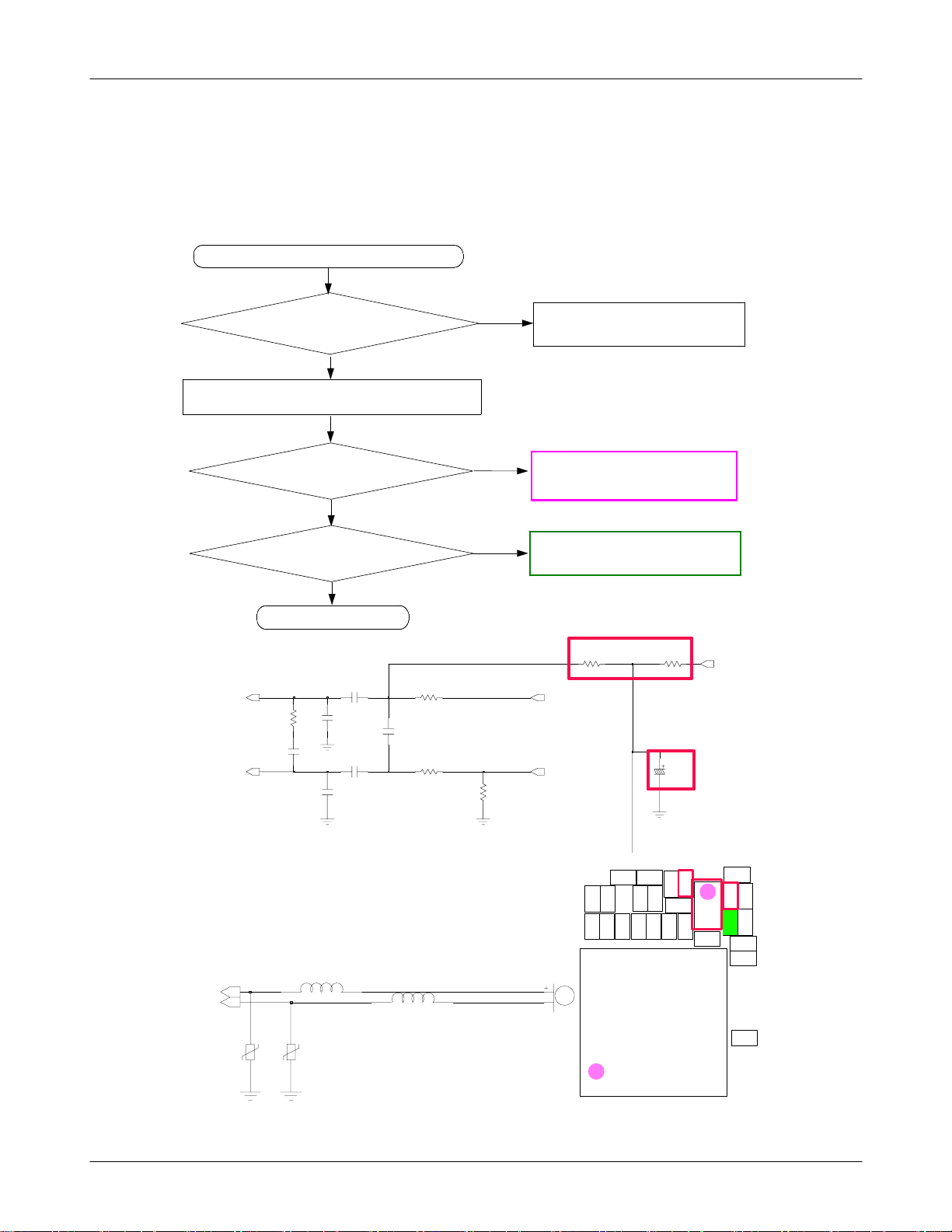
10-1-2. Initial
Flow Chart of Troubleshooting
Initial Failure
Yes
The Pin#A6 of UCP300 =
1.8V and
the Pin#D6 of UCP300 =
2.9V ?
Yes
Is the RST Pin#P5 of
UCP300 "Low→High" ?
Yes
There is 32.768kHz wave
forms at the C345 and C346
of OSC300
Is the SIM_RST Pin #B5 of
UCP300 is "High"
-
Yes
?
No
No
No
No
(if it has some problem, it is to be replaced.)
(if it has some problem, it is to be replaced.)
Check the
Check the
Check the
Check the
UCP300
UCP300
UCP300
UCP300
Yes
The voltage is "High" at the
C300,C301,C302,C303
Yes
LCD display is O.K
Yes
Sound is O.K
Yes
END
SAMSUNG Proprietary-Contents may change without notice
This Document can not be used without Samsung's authorization
No
No
No
10-3
Check the
Check the
Check the
UCP300
LCD
AUDIO
part
part
Flow Chart of Troubleshooting
0
4
9
L301
SIM_CLK
SIM_RST
UP_CLK
UP_RST
VRFLDO_1
VRFLDO_2
CNTL_DAT_CSP
CNTL_EN_CSP
HV_CHRG
BATKELV
PSW1_BUF
RTC_CLK
SCUSTB
SCANTST
RING_DRV
VIB_DRV
VIB_RNG_EN
SYSCLK
SYSCLKEN
RESETN
RESET_O
VAMICREF
VAMICRTN
VAREFRTN
VAVCMLSH
VAVCMRTN
CSN_PSC
SCLK_PSC
SDI_PSC
SDO_PSC
VBAT12
VBATAUD
VBATAUX
VBATRF
VBATSW
SIM_IO
X1RTC
X2RTC
VAREF
VAVCM
C311
C307
DCDC_OUT
GND_SW
VSIM
V_BATT
VRF_2.9V
C320
C313
C308
C309
C321
L301
V_BATT
C322
C346
OSC300
4
1
C345
2
3
B6
E6
B5
N5
L6
UP_IO
M6
E3
F3
F2
VREF
P1
N9
D10
G5
AFC
N7
AINT
B11
F1
CREF
L9
DINT
B12
FBSW
B13
LX
D3
NC1
L10
R3
P3
C9
VACC
A12
VEXT
F5
VRTC
C5
VSIM
N4
SCAN
K7
E8
E9
L7
N6
R6
R4
P5
G4
G3
K13
K10
K12
J11
L14
F13
K11
M10
P10
R10
M9
B10
VBAT
C6
E13
E11
E2
A14
1
NC
2
NC
L300
SIM1_CLK
SIM1_DATA
SIM1_RST
CNTL_DAT_CSP
CNTL_EN_CSP
AINT
DINT
PSW1_BUF
RTC_CLK
SCUSTB
MOTOR_EN
VIB_RNG_EN
CLK26M_ABB
CLK_REQ_ABB
FLASH_RST
RST
VAMICREF
C317
C318
UP_CS
UP_SCLK
UP_SDI
UP_SDO
C323
SIM_CLK
SIM_IO
SIM_RST
V_BATT
C324
VSYN_2.8V
C306
C310
C319
C
3
0
4
C310
L300
C
C
3
3
1
2
9
1
C313
TH300
R331
C340
C306
R303
C305
C320
C332
C331
C311
R306
C308
C307
C
3
2
7
C323
GND_SW
C
C
C
3
3
2
3
8
0
C
3
4
2
1
4
4
R
C
4
1
1
C
4
4
0
0
6
3
C318
C
4
2
4
C3
C3
0
0
3
P
C
U
C
C
3
C309
S
3
C
0
0
O
C345C346
C315
3
0
1
0
6
C
3
1
C301
10-4
SAMSUNG Proprietary-Contents may change without notice
This Document can not be used without Samsung's authorization
10-1-3. Sim Part
"Insert SIM is displayed on the LCD
Flow Chart of Troubleshooting
Yes
Check the SIM connector's
(SIM600) connection to
SIM card
Yes
Check the voltage at Pin#1
of SIM600 >= 2.9V ?
Yes
Is there any signals
Pin#13,#15,#16 of SIM600 ?
Yes
Check the SIM Card
END
No
No
No
Resolder or change
Check the
UCP300
Check the
SIM600
UCP300
VSIM
SIM_RST
SIM_CLK
C636
C635
C634
SIM600
6
11
33 4
7
C633 C634C632
C635
99
6
5
5
22
4
12 12
7
88
1111
10 10
G
G
1314GG1516
SIM_IO
C636
10-5
SAMSUNG Proprietary-Contents may change without notice
This Document can not be used without Samsung's authorization
C
6
3
2
SIM600
Flow Chart of Troubleshooting
10-1-4. Microphone Part
Microphone does not work
Yes
Is the assembled status of
microphone O.K?
Yes
Check the reference voltage on mic path
Yes
R402≒2.4V ?
Yes
Is microphone ok?
Yes
END
C402
MONO1_IN_P
C414
C403
C407
C412
R406
C411
R403
R409
R410
No
No
No
Reassembled the microphone
Resolder or change
R401,R402,C409
Check
UCP300
R401
MIC+
MIC-MONO1_IN_N
R402
VAMICREF
C409
MIC+
MIC-
VR400
R
4
R409R410
0
3
C
C
C
3
2
9
C
3
3
0
4
4
0
1
7
2
C402
R
C
C
C
4
4
3
4
0
1
2
1
6
4
4
1
0
0
3
P
C
U
L403
VR401
L404
MIC400
*
C
3
2
5
C
3
2
8
10-6
SAMSUNG Proprietary-Contents may change without notice
This Document can not be used without Samsung's authorization
R
R413
4
0
R
C318
C
C
4
4
0
2
4
2
2
0
9
R
C
4
4
1
2
4
4
C317
C302
C303
1
C
4
0
3
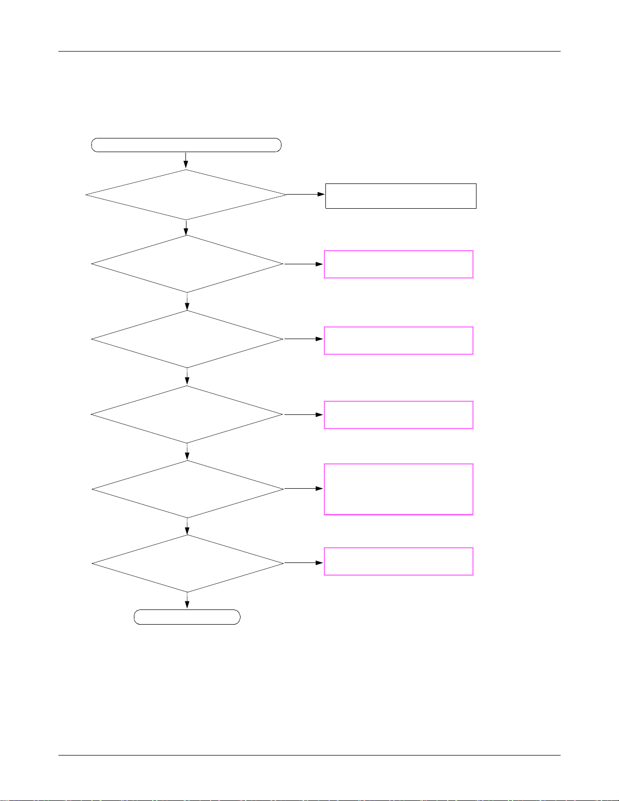
10-1-5. Receiver/Speaker Part
There is no sound from the Receiver/Speaker
Yes
Flow Chart of Troubleshooting
Is the terminal of
Receiver/Speaker O.K ?
Yes
Is SPK&MOT FPCB and
SUB PBA Connection O.K?
Yes
Is there any signals at the
Pin#5 and Pin#6 of CN102?
Yes
Is there any signals at the
Pin#3 and Pin#4 of CN100
Yes
Is there any signals at the
Pin#3 and Pin#4 of HDC600
Yes
No
No
No
No
No
Replace the SPK&MOT FPCB
Check SUB PBA AND
SPK&MOT FPCB Connection
Check
CN102(SUB PBA)
Resolder
(OR
Replace the SLIDE FPCB
Check
HDC600, U400(Audio AMP)
(OR
R431, R432 - Receiver.
C405, C406 - Speaker)
Resolder
L104, L105)
L408, L409,
Is there any signals at the
Pin#R13,Pin#R14,
Pin#12, Pin#P11
of UCP300 ?
Yes
END
SAMSUNG Proprietary-Contents may change without notice
This Document can not be used without Samsung's authorization
No
10-7
Check
UCP300
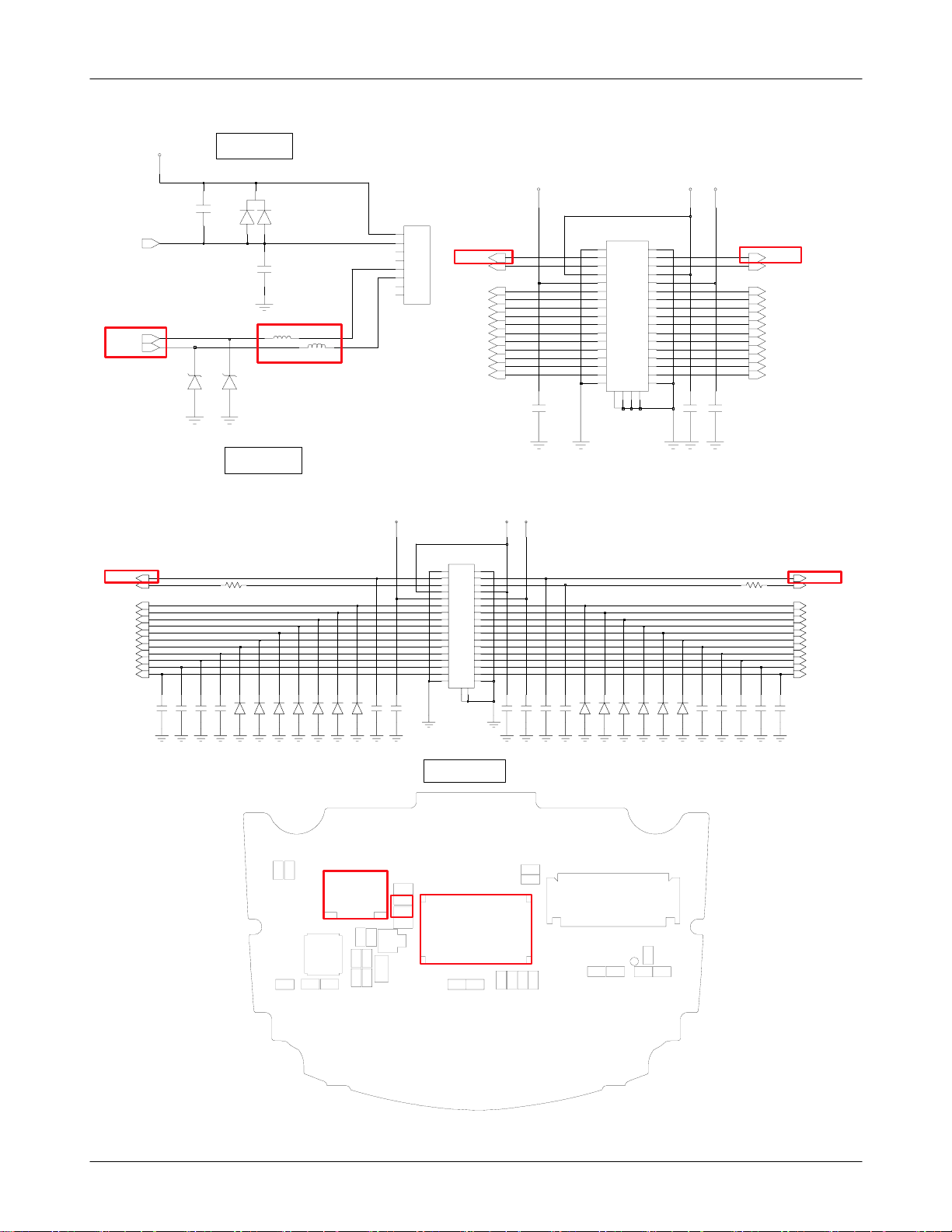
Flow Chart of Troubleshooting
MOTOR_EN
SPK+
SPK-
SPK_P
LCD_ID
D(5)
D(3)
D(1)
CP_OEN
CP_WEN
MEM_RST
D(7)
PWR_ON
KEY_COL(2)
KEY_COL(1)
KEY_COL(0)
V_BATT
MOTOR
3
C106
1
2
0
0
1
1
D
D
Z
Z
R603
C604 C602
C610
C605
D100
2
1
V101
L104
SPEAKER
ZD601
ZD600
ZD602
L105
ZD603
ZD604 ZD606
ZD605
VCCD_1.8V
C608
CN102
1
1
2
2
3
3
4
4
5
5
6
6
7
NC
8
NC
C607
SPK+
LCD_ID
LCD_D(5)
LCD_D(3)
LCD_D(1)
LCD_RD
LCD_WE
LCD_RST
LCD_D(7)
PWR_ON
KEY_COL(2)
KEY_COL(1)
KEY_COL(0)
1
2
1
3
4
3
56
6
5
778
9
10
9
11 12
11
12
13 14
13
14
15
16
15
17 18
17
18
19
20
19
212122
23 24
23
24
252526
27 28
27
28
29
30
29
313132
333334
NCNC
35
36
2
4
8
10
16
20
22
26
30
32
34
V_BATT
VCCD_2.9V
C631
C613
C606 C617
2
4
8
10
16
18
20
22
26
28
30
32
34
CN100
ZD607
2
4
6
8
10
12
14
16
18
20
22
24
26
28
30
32
34
NCNC36NC
35
37 38
ZD609ZD608
1
1
3
3
56
5
7
7
9
9
1112
11
1314
13
15
15
17
17
19
19
21
21
2324
23
25
25
27
27
29
29
31
31
33
33
NC
HDC600
VCCD_1.8V
V_BATT
ZD611ZD610
ZD612
VCCD_2.9V
C103
C611
C637
C102C104
R614
C601
SPKLCD_BL_EN
LCD_D(6)
LCD_D(4)
LCD_D(2)
LCD_D(0)
LCD_RS
LCD_CS
MOTOR_EN
KEY_SLIDE_EN
KEY_ROW(3)
KEY_ROW(4)
KEY_COL(3)
SPK_N
LCD_BL_EN
D(6)
D(4)
D(2)
D(0)
A(2)
LCD_CS
MOTOR_EN
KEY_SLIDE_EN
KEY_ROW(3)
KEY_ROW(4)
KEY_COL(3)
C619C600
LCD CON
V
V
1
0
7
L103
1
0
4
CN102
U100
C100
R101
ZD101
L105
L104
ZD102
C
V
D
1
1
1
0
0
0
6
1
0
C
C
1
1
C
0
0
7
1
1
C
0
V
1
1
3
1
0
2
9
L101
C
N
1
0
0
C114
V103
V100
CN101
C
1
0
2
V
L
C
V
1
1
1
1
0
0
1
0
2
5
5
8
C104
R108
TP100
L100
C113
10-8
SAMSUNG Proprietary-Contents may change without notice
This Document can not be used without Samsung's authorization
 Loading...