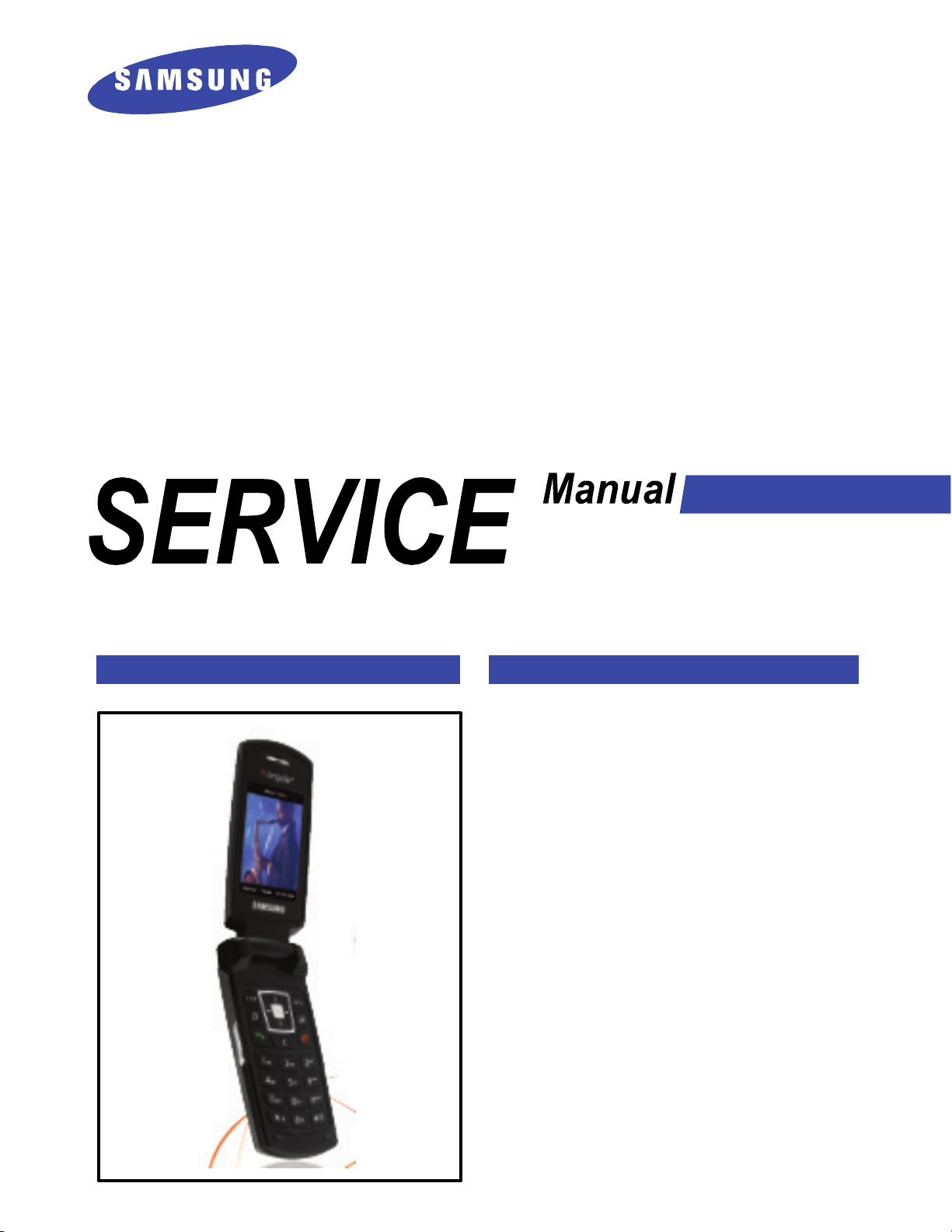
Samsung SGH-A707 Service Manual
efrcom
UMTS TELEPHONE
SGH-A707
UMTS TELEPHONE
CONTENTS
1. Safety Precautions
2. Specification
3. Product Function
4. Array course control
5. Exploded View/Disassembly
and Assembly Instructions
6. MAIN Electrical Parts List
7. Block Diagrams
8. PCB Diagrams
9. Flow Chart of Troubleshooting
10. Reference data

This Service Manual is a property of Samsung Electronics Co.,Ltd.
Any unauthorized use of Manual can be punished under applicable
International and/or domestic law.
ⓒ
Samsung Electronics Co.,Ltd.
2006. 10. Rev.1.0

CONTENTS
1. Safety Precautions
1-1. Repair Precaution......................................................................................................1-1
1-2. ESD(Electrostatically Sensitive Devices) Precaution...............................................1-2
2. Specification
2-1. GSM General Specification.......................................................................................2-1
2-2. GSM Tx Power Class...............................................................................................2-2
3. Product Function
4. Array course control
4-1. Software Adjustments................................................................................................4-1
4-2. Software Downloading...............................................................................................4-2
5. Exploded View/Disassembly & Assembly Instructions
5-1. Cellular phone Exploded View..................................................................................5-1
5-2. Cellular phone Parts list............................................................................................5-2
5-3. Disassembly & Assembly Instructions......................................................................5-5
6. MAIN Electrical Parts List
7. Block Diagrams
7-1. Base Band Block Diagram........................................................................................7-1
7-2. RF Block Diagram.....................................................................................................7-2
8. PCB Diagrams

CONTENTS
9. Flow Chart of Troubleshooting
9-1. Power On..................................................................................................................9-1
9-2. Initial...........................................................................................................................9-3
9-3. Sim Part.....................................................................................................................9-4
9-4. Microphone Part-Phone MIC....................................................................................9-7
9-5. Microphone Part-Earphone MIC...............................................................................9-9
9-6. Earphone Part.........................................................................................................9-11
9-7. Receiver Part..........................................................................................................9-14
9-8. Speaker Part...........................................................................................................9-16
9-9. Key Data Input........................................................................................................9-20
9-10. Back Light(for Color Main LCD)..........................................................................9-21
9-11. Key Back Light.....................................................................................................9-22
9-12. Camera Part..........................................................................................................9-23
9-13. Touch PAD...........................................................................................................9-24
9-14. GSM Receiver......................................................................................................9-26
9-15. GSM Transmitter..................................................................................................9-28
9-16. DCS Receiver.......................................................................................................9-30
9-17. DCS Transmitter...................................................................................................9-32
9-18. PCS Receiver.......................................................................................................9-34
9-19. PCS Transmitter...................................................................................................9-37
9-20. WCDMA850 Receiver...........................................................................................9-39
9-21. WCDMA850 Transmitter.......................................................................................9-41
9-22. WCDMA1900 Receiver.........................................................................................9-44
9-23. WCDMA1900 Transmitter.....................................................................................9-46
10. Reference data

1. Safety Precautions
1-1. Repair Precaution
●
Repair in Shield Box, during detailed tuning.
Take specially care of tuning or test, because the specification of cellular phone is sensitive for
surrounding interference(RF noise).
●
Be careful to use a kind of magnetic object or tool, because performance of parts is damaged by the
influence of magnetic force.
●
Surely use a standard screwdriver when you disassemble this product, otherwise screw will be worn
away.
●
Use a thicken twisted wire when you measure level.
A thicken twisted wire has low resistance, therefore error of measurement is few.
●
Repair after separate Test Pack and Set because for short danger (for example an
overcurrent and furious flames of parts etc) when you repair board in condition of
connecting Test Pack and tuning on.
●
Take specially care of soldering, because Land of PCB is small and weak in heat.
●
Surely tune on/off while using AC power plug, because a repair of battery charger is
dangerous when tuning ON/OFF PBA and Connector after disassembling charger.
●
Don't use as you pleases after change other material than replacement registered on SEC System.
Otherwise engineer in charge isn't charged with problem that you don't keep this rules.
1-1
SAMSUNG Proprietary-Contents may change without notice
This Document can not be used without Samsung's authorization

Safety Precautions
1-2. ESD(Electrostatically Sensitive Devices) Precaution
Several semiconductor may be damaged easily by static electricity. Such parts are called by ESD
(Electrostatically Sensitive Devices), for example IC,BGA chip etc. Read Precaution below.
You can prevent from ESD damage by static electricity.
●
Remove static electricity remained your body before you touch semiconductor or parts with
semiconductor. There are ways that you touch an earthed place or wear static electricity
prevention string on wrist.
●
Use earthed soldering steel when you connect or disconnect ESD.
●
Use soldering removing tool to break static electricity. , otherwise ESD will be damaged by
static electricity.
●
Don't unpack until you set up ESD on product. Because most of ESD are packed by box and
aluminum
plate to have conductive power,they are prevented from static electricity.
●
You must maintain electric contact between ESD and place due to be set up until ESD is connected
completely to the proper place or a circuit board.
1-2
SAMSUNG Proprietary-Contents may change without notice
This Document can not be used without Samsung's authorization

2. Specification
2-1. GSM General Specification
GSM 850 EGSM 900 DCS1800 PCS1900
Freq.
Band[MHz]
Uplink/Downli
nk
ARFCN range 128~25
Tx/Rx spacing 45MHz 45MHz 95MHz 80MHz 45MHz 80MHz
Mod. Bit rate/
Bit Period
Time Slot
Period/Frame
Period
Modulation 0.3GMSK 0.3GMSK 0.3GMSK 0.3GMSK
824~849
869~894
270.833kbp
s
3.692us
576.9us
4.615ms
880~915
925~960
0~124 &
975~1023
270.833kbp
s
3.692us
576.9us
4.615ms
1710~1785
1805~1880
512~885 512~810
270.833kbp
s
3.692us
576.9us
4.615ms
1850~1910
1930~1990
270.833kbp
s
3.692us
576.9us
4.615ms
W-CDMA
850
824~849
869~894
UL:4132~42
33
DL:4357~44
58
3.84Mcps 3.84Mcps
Frame
length :
10ms
Slot length
: 0.667ms
QPSK
HQPSK
W-CDMA
1900
1850~1910
1930~1990
UL:9262~95
38
DL:9662~99
38
Frame
length :
10ms
Slot length
: 0.667ms
QPSK
HQPSK
MS Power
Power Class
Sensitivity -102dBm -102dBm -100dBm -100dBm -106.7dBm -106.7dBm
TDMA Mux 8 8 8 8
Cell Radius 35Km 35Km 2Km 2Km 2Km 2Km
33dBm~5dBm33dBm~5dBm30dBm~0dBm30dBm~0dBm24dBm ~ -
50dBm
4
(max
+33dBm)
4
(max
+33dBm)
1
(max
+30dBm)
1
(max
+30dBm)
3
(max
+24dBm)
24dBm ~ -
50dBm
3
(max
+24dBm)
2-1
SAMSUNG Proprietary-Contents may change without notice
This Document can not be used without Samsung's authorization
Specification
2-2. GSM TX power class
TX Power
control level
533±2dBm
631±2dBm
729±2dBm
827±2dBm
925±2dBm
10 23±2 dBm
11 21±2 dBm
GSM850
GSM900
TX Power
control level
030±3dBm
128±3dBm
226±3dBm
324±3dBm
422±3dBm
520±3dBm
618±3dBm
DCS1800
TX Power
control level
030±3dBm
128±3dBm
226±3dBm
324±3dBm
422±3dBm
520±3dBm
618±3dBm
PCS1900
12 19±2 dBm
13 17±2 dBm
14 15±2 dBm
15 13±2 dBm
16 11±3 dBm
17 9±3 dBm
18 7±3 dBm
19 5±3 dBm
716±3dBm
814±3dBm
912±4dBm
10 10±4 dBm
11 8±4 dBm
12 6±4 dBm
13 4±4 dBm
14 2±5 dBm
716±3dBm
814±3dBm
912±4dBm
10 10±4 dBm
11 8±4 dBm
12 6±4 dBm
13 4±4 dBm
14 2±5 dBm
15 0±5 dBm
2-2
15 0±5 dBm
SAMSUNG Proprietary-Contents may change without notice
This Document can not be used without Samsung's authorization

3. Product Function
Main Function
―
Bluetooth
―
Camera and camcorder
―
Instant Messaging capability
―
E-mail
―
Featured applications provide alarms, calendar, calculator, record audio, converter, timer,
stopwatch, and world time.
―
File viewer
―
Name card
―
Multimedia Message Service (MMS)
―
Multimedia capability (with included Media player)
―
Photo caller ID
―
Speakerphone capability
―
Web browser
3-1
SAMSUNG Proprietary-Contents may change without notice
This Document can not be used without Samsung's authorization

Product Function
3-2
SAMSUNG Proprietary-Contents may change without notice
This Document can not be used without Samsung's authorization
4. Array course control
4-1. Software Adjustments
12
34
4
56
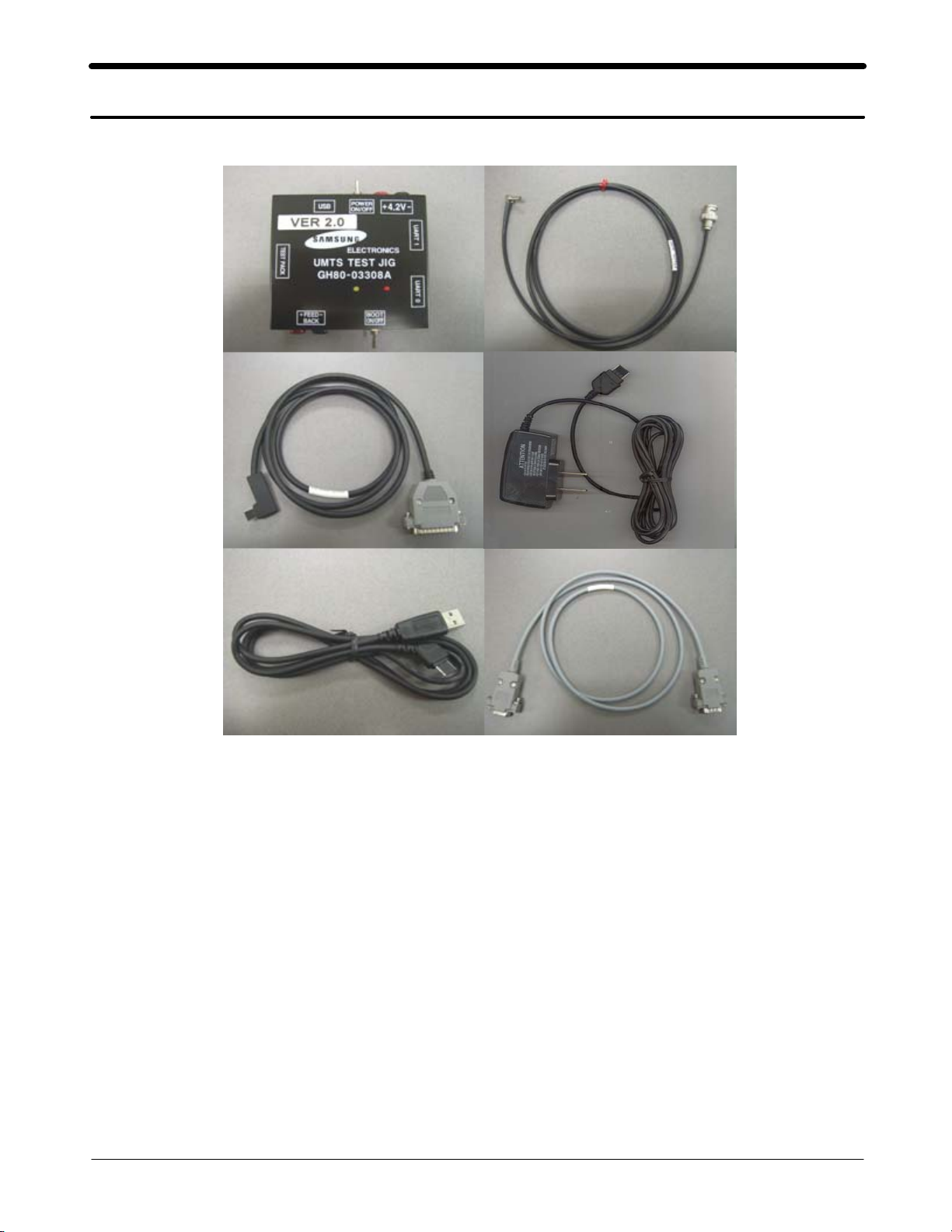
1. JIG(GH80-03308A): Download, Trace, Calibration, etc
2. RF test cable: RF test
3. Test cable(GH39-00558A): JIG to phone
4. TA (Travel Adaptor)
5. Data Link Cable (PCB200BBE): USB cable
6. Serial cable: PC to JIG
4-1
SAMSUNG Proprietary-Contents may change without notice
This Document can not be used without Samsung's authorization
Array course control
4-2. Software Download
4-2-1. Pre-requsite for Download
• Downloader Program(
FastMultiLoader V3.28.exe
)
• SGH-A707 Mobile Phone
• USB Data Link Cable
• Binary files
4-2-2. S/W Download Process
■
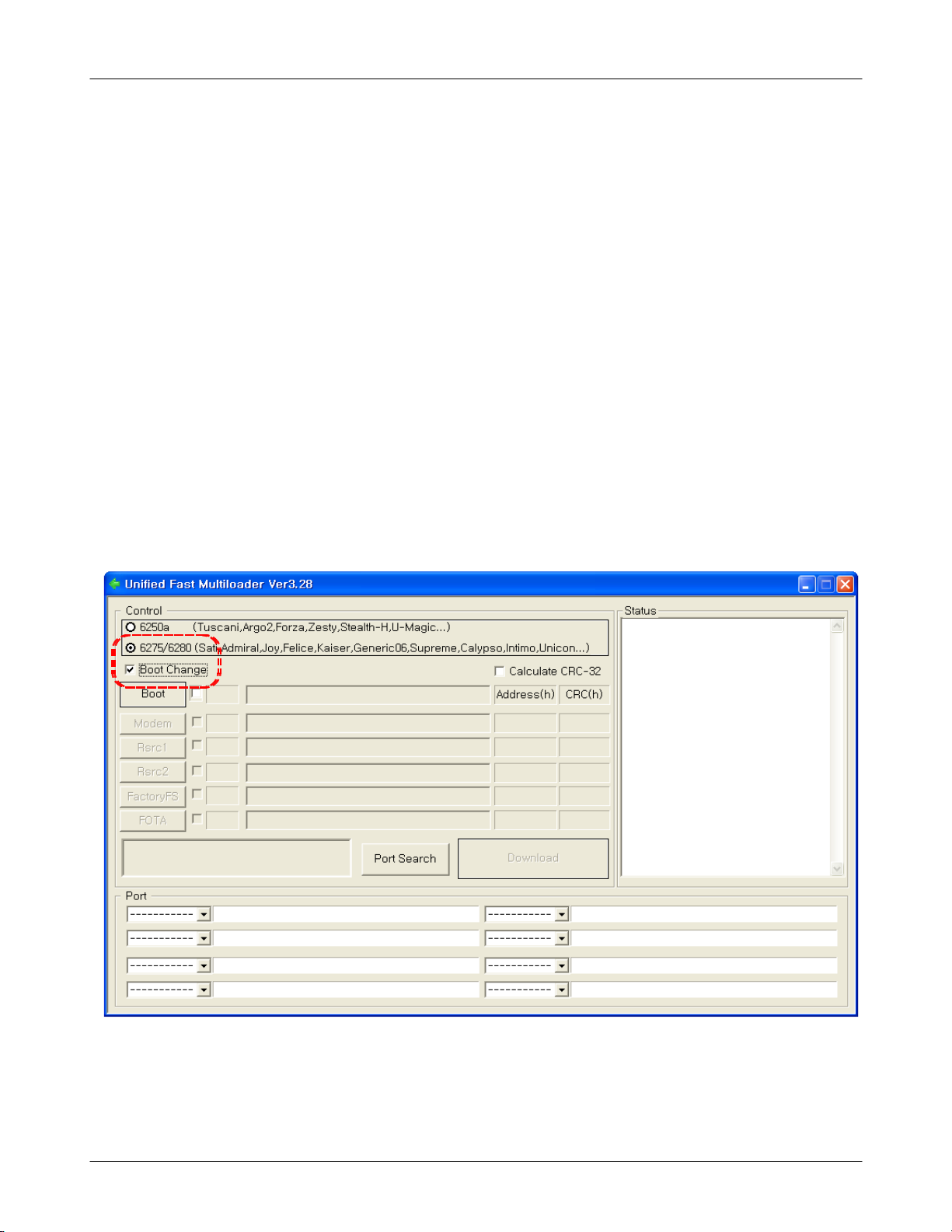
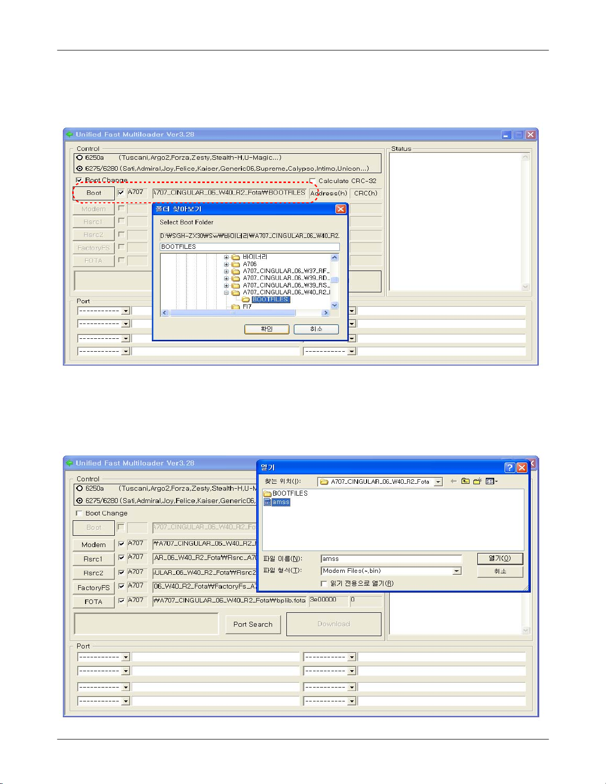
Load the binary download program by executing the
“
FastMultiLoader V3.28.exe
. First, select the 6275/6280 for 'admiral'. And check 'Boot Change', then the 'Boot'
1
”
will be activated.
4-2
SAMSUNG Proprietary-Contents may change without notice
This Document can not be used without Samsung's authorization
Array course control
. Click the 'Boot', then the dialogue box is opened, then select the wanted file. And
2
select 'OK'.
. Select the 'Boot Change' once more, then 'Boot' is inactivated, and the
3
others('modem', 'Rsrc1', 'Rsrc2', 'FactoryFS', and 'Fota') are activated.
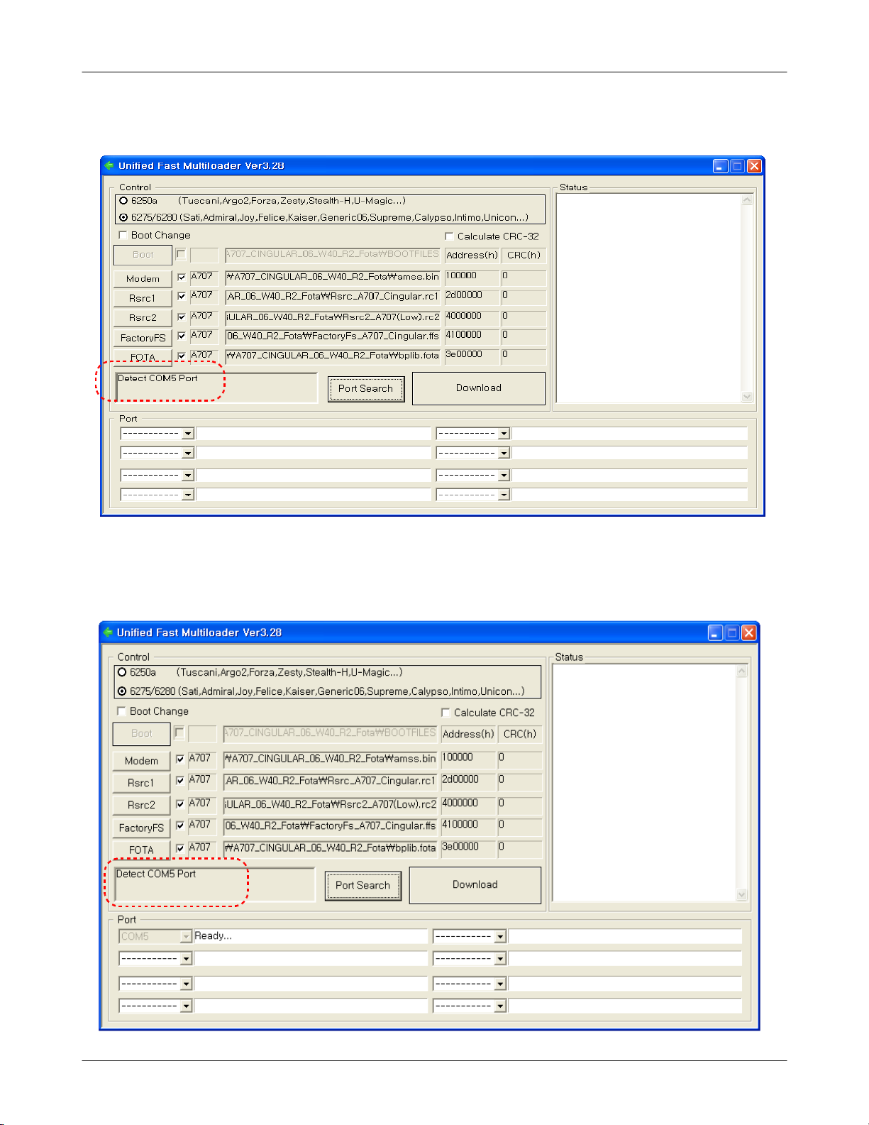
- Click 'modem', 'Rsrc1', 'Rsrc2', 'FactoryFS' and 'FOTA' each, and select
wanted files.
4-3
SAMSUNG Proprietary-Contents may change without notice
This Document can not be used without Samsung's authorization
Array course control
. Connect phone to cable, the 'Detect Com port' is displayed.
4
. Select 'Port Search', then 'Port' is activated.
5
4-4
SAMSUNG Proprietary-Contents may change without notice
This Document can not be used without Samsung's authorization
Array course control
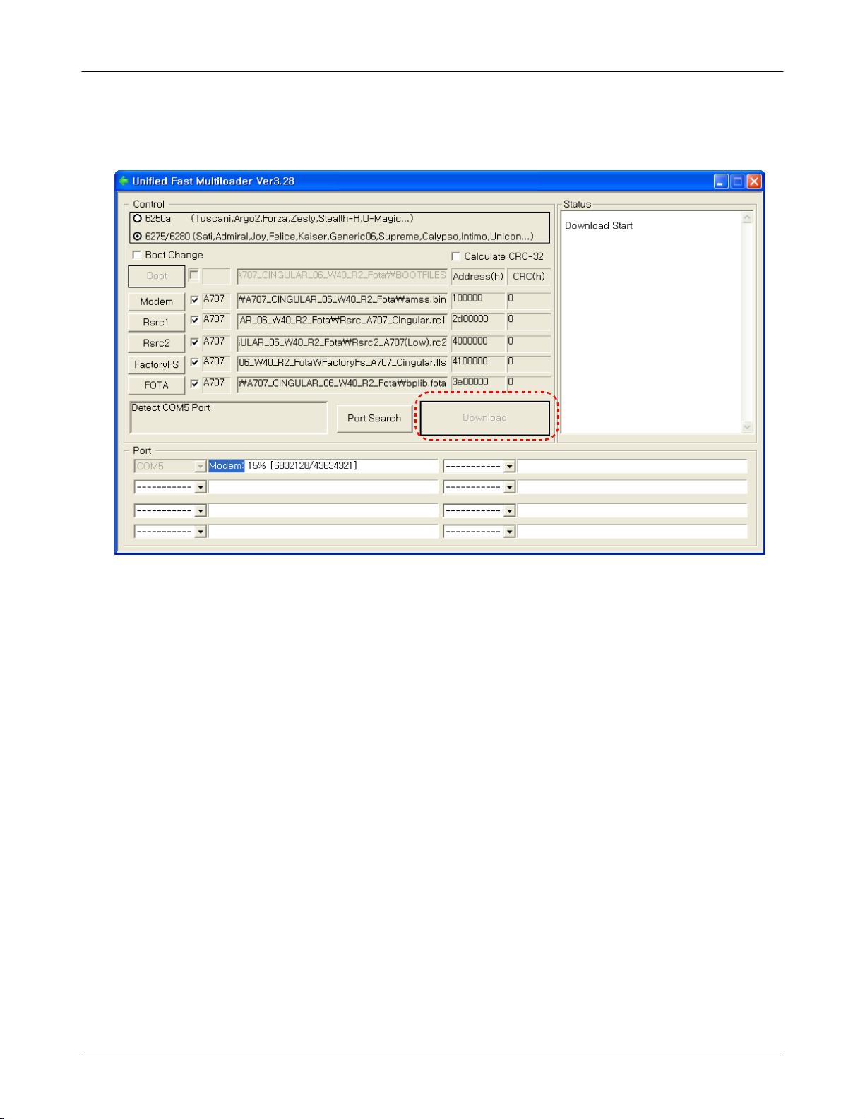
. Click 'Download', then downloading is executed successively.If the download is
6
completed, S/W downloading is finished.
4-5
SAMSUNG Proprietary-Contents may change without notice
This Document can not be used without Samsung's authorization

Array course control
4-6
SAMSUNG Proprietary-Contents may change without notice
This Document can not be used without Samsung's authorization
5. Exploded View/Disassembly&Assembly Instructions
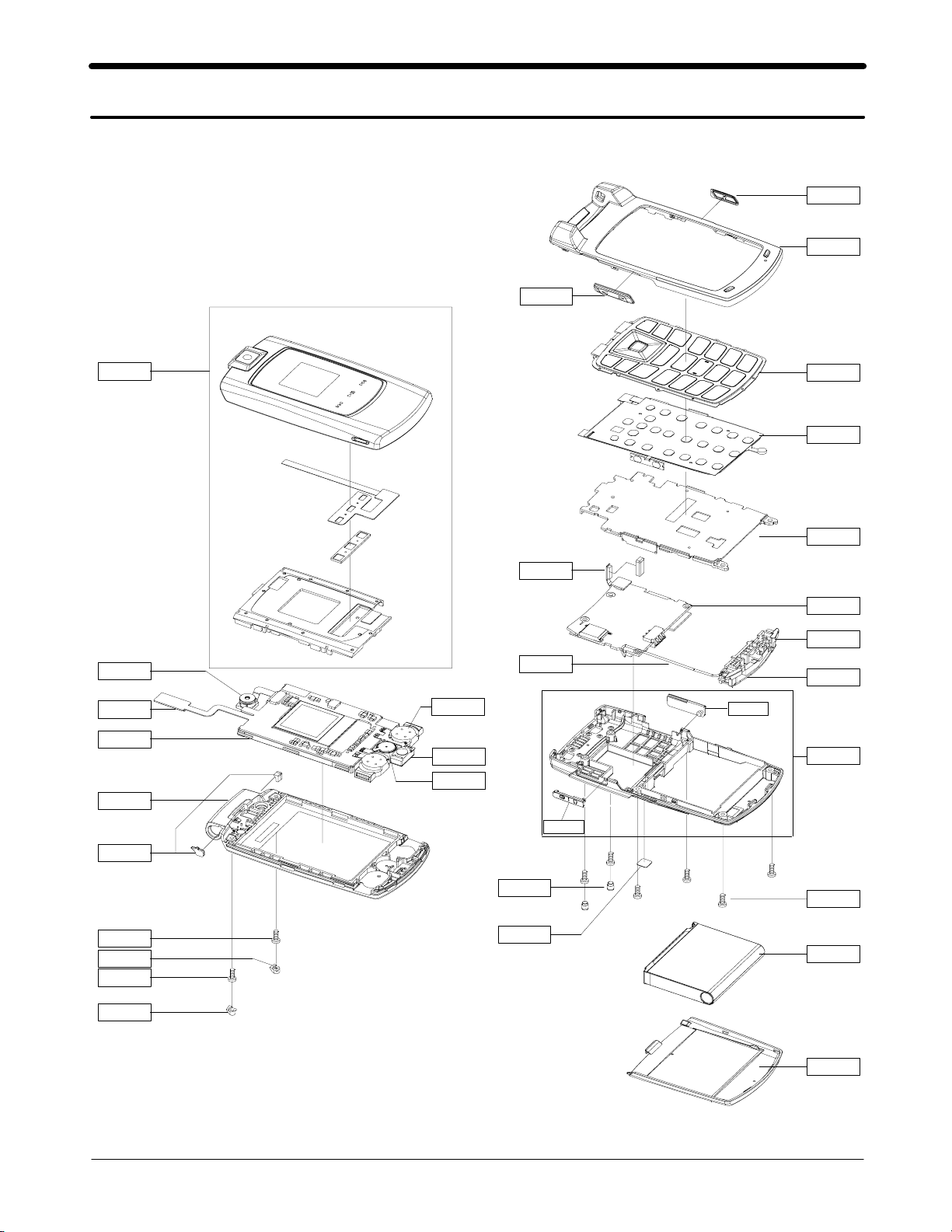
5-1. Cellular phone Exploded View
QVO01
QCK01
QFR01
QFU01
QCA02
QME03
QLC01
QFL01
QME06
QME05
QM001
QKP01
QME01
QSH01
QAN01
QMP01
QAN06
QCB01
QAN02
QSD01
QRE01
QIF01
QSC01
QCR52
QSC08
QCR52
QSC05
QSC13
QRF01
5-1
SAMSUNG Proprietary-Contents may change without notice
This Documen t can not be used without Samsung's authorization
QCR04
QBA01
QBA00
Exploded View/Disassembly&Assembly Instructions
5-2. Cellular phone Parts list
Design LOC Description SEC CODE
QAN01
QAN02
QAN06
QBA00
QBA01
QCA02
QCB01
QCK01
QCR04
QCR52
QFL01
QFR01
QFU01
QKP01
QLC01
QME01
QME01
QME05
QME06
QMO01
QMP01
QRF01
QSC01
QSC05
QSC08
QSC13
QSH01
QVO01
QRE01
QIF01 PMO-COVER IF GH72-35076A
QSD01 PMO-COVER SD GH72-35077A
INNER BATTERY PACK-1100MAH,BLK GH43-02651A
MEA-FOLDER UPPER KIT(DARK_GRAY GH97-06714A
ELA ETC-SGHA707 LCD MODULE SVC GH96-02265A
UNIT-RECEIVER SPEAKER FPCB ASS GH59-03717A
FPCB ANTENNA CHIP GH42-00794A
INTENNA-SGHA707 GH42-01011A
ASSY COVER-INTENNA CARRIER GH98-02961A
PMO-CASE BATTERY V2 GH72-33925A
UNIT-CAMERA GH59-03706A
CBF COAXIAL CABLE-SGHA701 GH39-00693A
ASSY KEY-CAMERA GH98-03118A
SCREW-MACHINE 6001-001479
SCREW-MACHINE 6001-001300
ASSY CASE-FOLDER LOWER GH98-01631A
ASSY CASE-FRONT COVER GH98-02448A
ASSY KEYPAD-(XET/BLK) GH98-02288A
UNIT-LCD CON TO CON FPCB GH59-03780A
UNIT-MAIN KEY FPCB GH59-03719A
UNIT-SPEAKER FPCB ASSY GH59-03718A
MOTOR DC-SGHA707 GH31-00279A
PBA MAIN-SGHA707 GH92-03216A
MPR-TAPE COVER RF GH74-27477A
PMO-DECO FOLDER LOWER L GH72-33926A
RMO-RUBBER COVER LOWER L GH73-07621A
RMO-RUBBER COVER LOWER R GH73-07622A
RMO-RUBBER COVER REAR GH73-07623A
ASSY BRACKET-SHIELD GH98-01635A
PMO-KEY VOL GH72-30608A
ASSY CASE-REAR GH98-01633A
5-2
SAMSUNG Proprietary-Contents may change without notice
This Documen t can not be used without Samsung's authorization
Exploded View/Disassembly&Assembly Instructions
Description Sec Code
BAG PE 6902-000634
ADAPTOR-SGHE690,BLK,USA GH44-01363A
LABEL(P)-WATER SOAK GH68-02026A
LABEL(R)-WATER SOAK T_MOBILE GH68-05914A
LABEL(P)-UNIT BARCODE CIN GH68-09418A
MANUAL USERS-CINGULAR SPANISH GH68-12489A
MANUAL USERS-CINGULAR ENGLISH GH68-12490A
MANUAL USERS-CINGULAR ENGLISH GH68-12491A
MANUAL USERS-CINGULAR ENGLISH GH68-12492A
LABEL(R)-MAIN(CIN) GH68-12720A
LABEL-QUALCOMM GH68-12830A
MANUAL USERS-NAPSTER PROMOTION GH68-12914A
CUSHION-CASE(CIN) GH69-04506A
BOX-UNIT(CIN) GH69-04507A
RMO-RUBBER B/T GH73-07213A
MPR-REMOVE TAPE LCD GH74-13804A
MPR-BOHO VINYL LCD CONN GH74-15350A
MPR-TAPE FPCB DOUBLE GH74-16772A
CONE-TAPE SUB LCD INSUL GH74-19756A
MPR-TAPE,33X53X0.16,TESA4976 GH74-26578A
MPR-INSU TAPE GH74-27074A
MPR-INSU TAPE GH74-27077A
MPR-TAPE GH74-27078A
MPR-INSU TAPE GH74-27110A
MPR-INSU TAPE GH74-27324A
MPR-GASK TAPE GH74-27325A
MPR-INSU TAPE GH74-27436A
MPR-GASK TAPE GH74-27437A
MPR-INSU TAPE GH74-27751A
MPR-SPONGE SPK 1 GH74-28132A
MPR-VINYL BOHO SUB WINDOW GH74-28184A
MPR-TAPE J TAG GH74-28232A
MPR-VINYL BOHO MAIN WIN PRESS GH74-28233A
MPR-GASK TAPE GH74-28263A
MPR-SPONGE SIM GH74-28585A
MPR-SPONGE PCB 1 GH74-28596A
MPR-SPONGE PCB 2 GH74-28597A
MPR-SPONGE LOWER L GH74-28600A
MPR-SPONGE LOWER R GH74-28601A
5-3
SAMSUNG Proprietary-Contents may change without notice
This Documen t can not be used without Samsung's authorization
Exploded View/Disassembly&Assembly Instructions
Description Sec Code
MPR-GASK TAPE SHIELD GH74-28602A
MPR-TAPE LOWER SCREW GH74-28625A
MPR-VINYL BOHO WINDOW MAIN LOG GH74-28660A
MPR-TAPE LABEL INTENNA GH74-28783A
AS-SGHA701 MIC SVC GH81-06074A
ASSY COVER-MAIN WINDOW GH98-02935A
5-4
SAMSUNG Proprietary-Contents may change without notice
This Documen t can not be used without Samsung's authorization
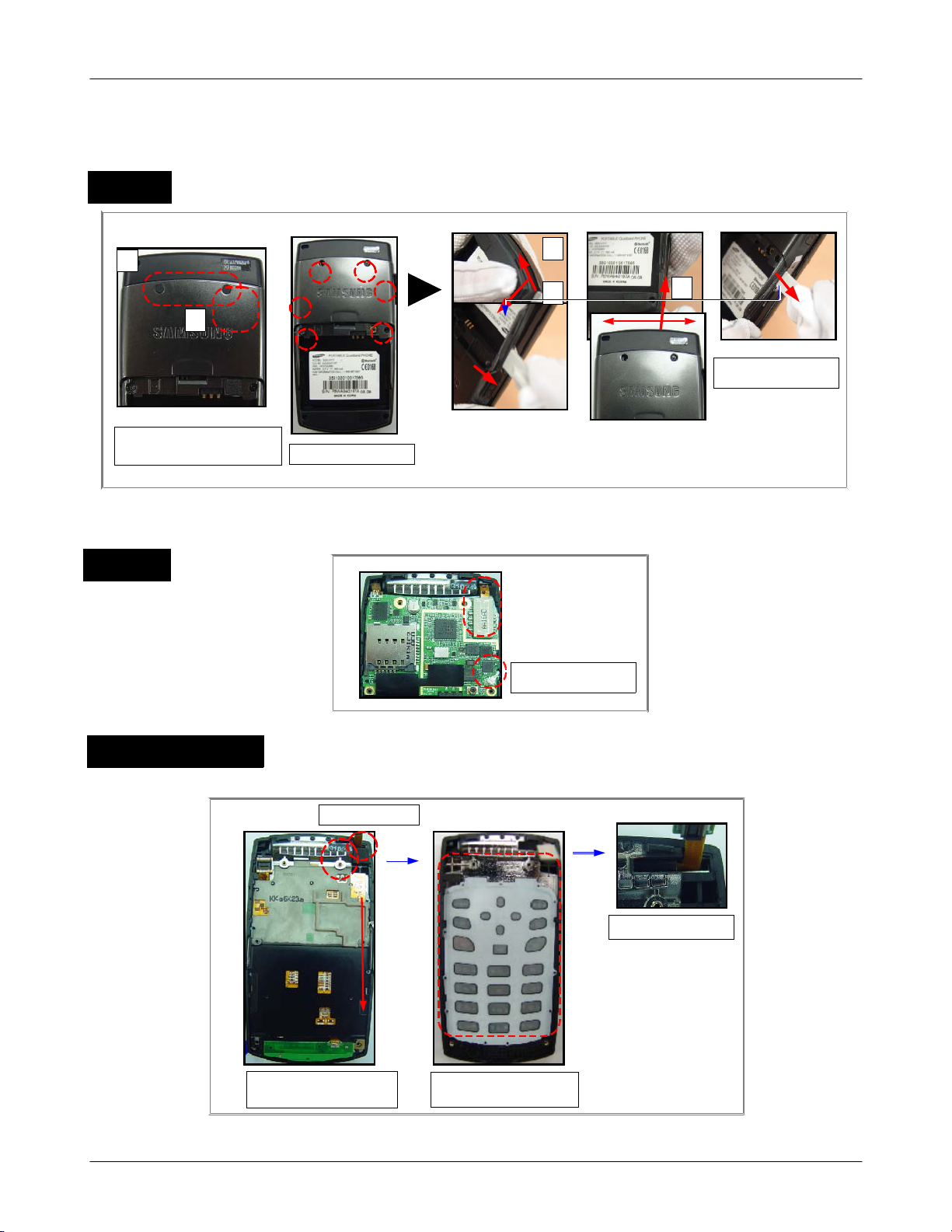
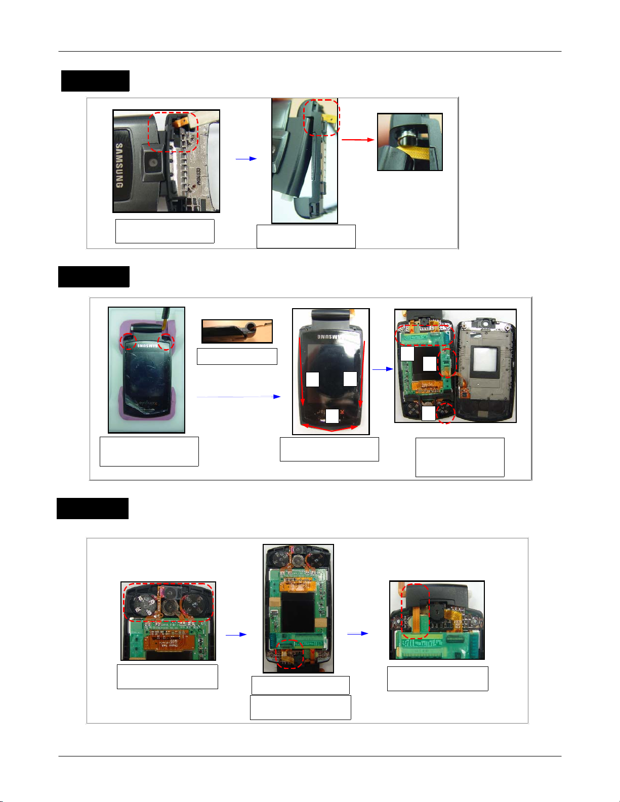
5-3. Disassembly and Assembly Instructions
―
Disassembly
1.REAR
Exploded View/Disassembly&Assembly Instructions
1
2
1.Remove REAR Screw cap(2points)
2.Dettach the RF Sheet
2.PBA
Unscrew 6EA on the rear
2
1
LCD * COXIAL CONNECTOR
disassembly
3
Separate the rear by
shaking the hooker
3.SHIELDCAN & KEYPAD
Dettach the Sponge
Remove FRONT DUST TAPE
Separate the shieldcan
downward by disassembly tool
Separate the KEYPAD
Caution : RIB of the FRONT
5-5
SAMSUNG Proprietary-Contents may change without notice
This Documen t can not be used without Samsung's authorization
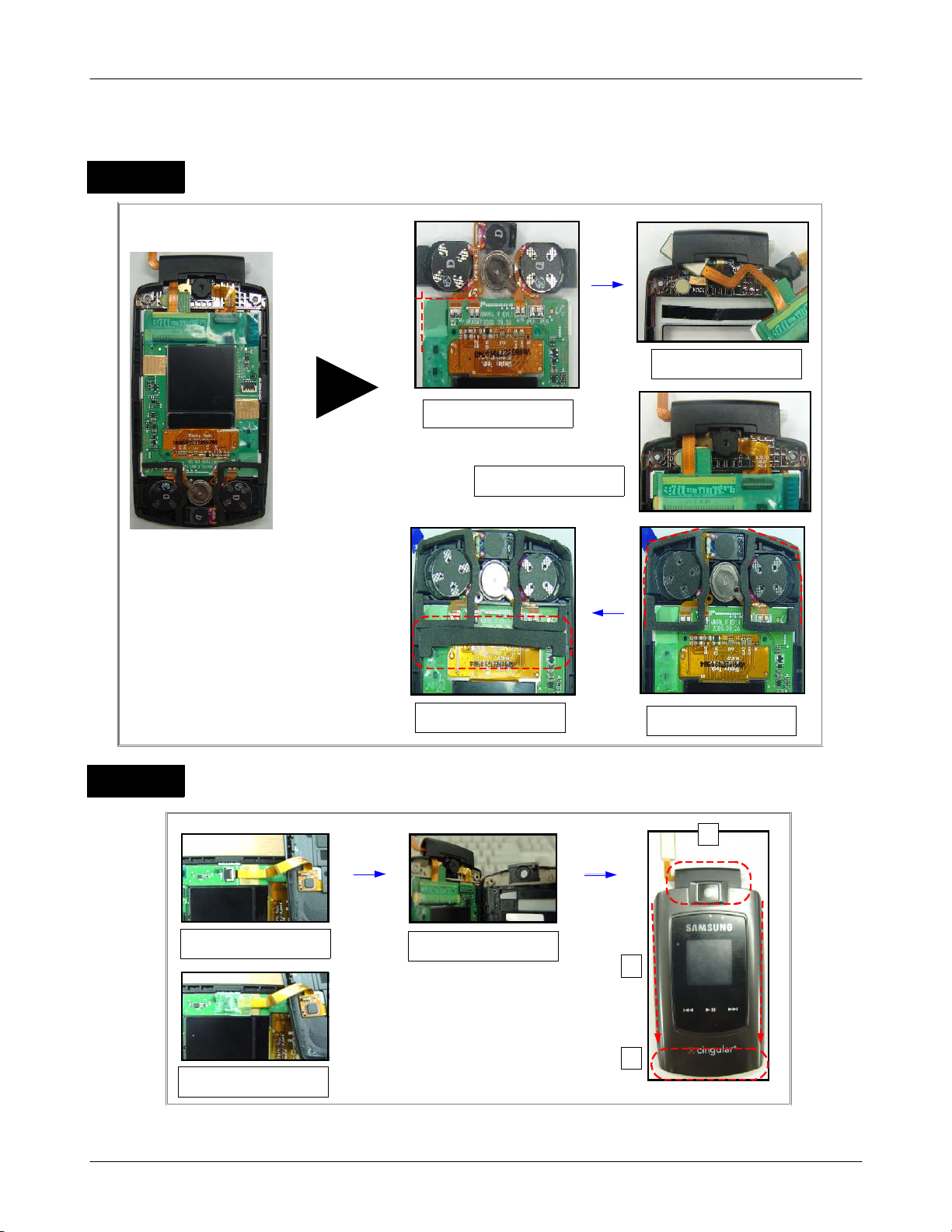
Exploded View/Disassembly&Assembly Instructions
4.FOLDER
5.FOLDER
6.LCD
Separate FRONT from FOLDER
pushing the hinge by driver
Remove SCREW TAPE after
removing SCREW RUBBER
==> UNSCREW 2EA
Separate Deco Lower L
Separate FOLDER from FRONT
=> Be cautious breaking FPCB
1
3
Separate Lower from Folder
pushing outward like 1 → 3
1
3
2
2
1.Remove Green Tape
2.Remove the SPONGE
3.Remove green tape
& Disassambly connector
Separate spk/rcv ,spk and motor
using tweezers
SAMSUNG Proprietary-Contents may change without notice
This Documen t can not be used without Samsung's authorization
Separate CAM using tweezers
Dettach the cam module
5-6
Separate LCD FPCB from Front
hole
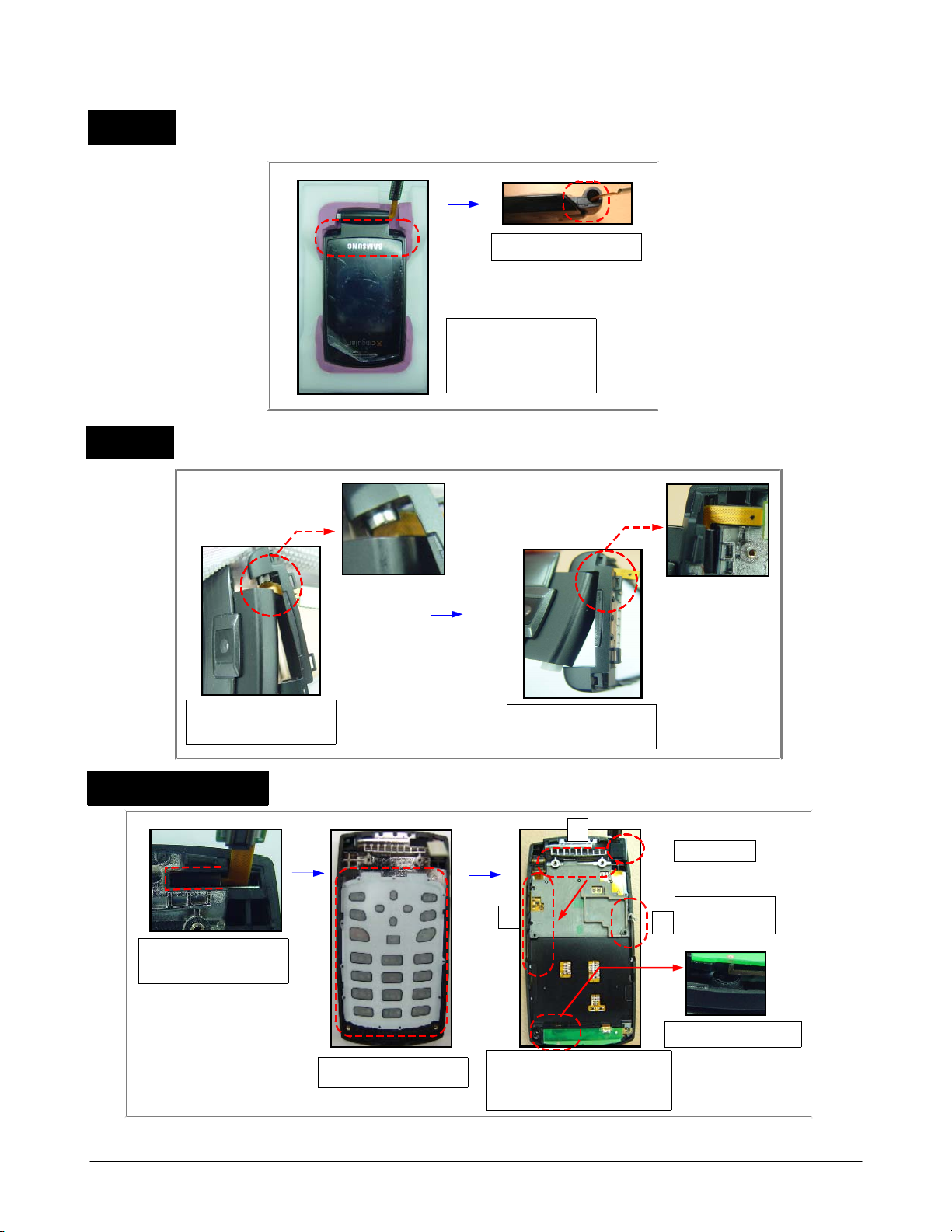
―
1.LCD
Exploded View/Disassembly&Assembly Instructions
Assembly
Insert FPCB in 45˚
=> Caution : Breaking FPCB
Attach Green TPAE
Insert CAM in the LOWER's RIB
=> Pushing 2~3 times
2.FOLDER
Insert FPCB와 in the parallel
of silk line of PCB
Refer the silk line of PCB
=> Caution : SUB LCD
Attach Sponge in the line of
LCD's upper EDGE
Connect LOWER and upper HOOKER
of the Front
5-7
Attach Sponge in the line of
LOWER EDGE
1
3
2
SAMSUNG Proprietary-Contents may change without notice
This Documen t can not be used without Samsung's authorization
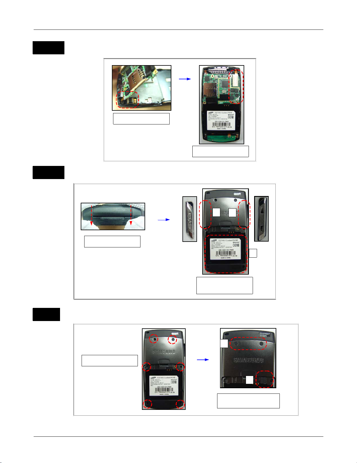
Exploded View/Disassembly&Assembly Instructions
3.SCREW
4.FRONT
Assembly Deco Lower L
SCREW M1.7 L2.5
=> 1.0 ± 0.1Kgf/㎠
=> Attach SCREW TAPE
=> Pushing after inserting
SCREW RUBBER
Insert FPCB of the Folder in
the hole of Front
=> Caution : Breaking FPCB
5.SHIELDCAN & KEYPAD
Attach in the line of hole of
the FRONT
=> Pushing 1~2 times
Insert all the holes of KEYPAD
into the RIB of FRONT
Insert the FPCB of the Folder
into the hole of the FRONT
=> Caution : Breaking FPCB
1
2
① Connect SHIELDCAN to BOSS HOLE
② Insert the hole of Shieldcan into
HOOKER
③ insert into the right HOOKER
5-8
Sponge Attach
Caution : COXIAL
3
CABLE`s Cutting
Check the MIC connection
SAMSUNG Proprietary-Contents may change without notice
This Documen t can not be used without Samsung's authorization
6.PBA
7.REAR
Exploded View/Disassembly&Assembly Instructions
Connect KEY PCB after
Inserting antenna connector
Connector LCD FPCB, Antenna
COXIAL cable
8.SCREW
Connect Hooker pushing
downward
SCREW M1.4 L4.0
=> 1.1 ± 0.1Kgf/㎠
2
2
② Check side key direction
line upper figure
③ Connector lower HOOKER
1
3
2
1.Insert REAR Screw cap(2points)
2.Attach the RF Sheet
5-9
SAMSUNG Proprietary-Contents may change without notice
This Documen t can not be used without Samsung's authorization

Exploded View/Disassembly&Assembly Instructions
5-10
SAMSUNG Proprietary-Contents may change without notice
This Documen t can not be used without Samsung's authorization
6. MAIN Electrical Parts List
Design LOC Description SEC Code STATUS
ANT400 CONNECTOR-COAXIAL 3705-001225 SA
BAT200 BATTERY-LI(2ND) 4302-001180 SA
BT200 BLUETOOTH MODULE 4709-001445 SA
BTC300 CONNECTOR-BATTERY 3711-006003 SA
C100 C-CER,CHIP 2203-006423 SA
C101 C-CER,CHIP 2203-006423 SA
C102 C-CER,CHIP 2203-006423 SA
C103 C-CER,CHIP 2203-006423 SA
C104 C-CER,CHIP 2203-006423 SA
C105 C-CER,CHIP 2203-000489 SA
C106 C-CER,CHIP 2203-000628 SA
C107 C-CER,CHIP 2203-006423 SA
C108 C-CER,CHIP 2203-006423 SA
C109 C-CER,CHIP 2203-006423 SA
C110 C-CER,CHIP 2203-000628 SA
C111 C-CER,CHIP 2203-006562 SA
C112 C-CER,CHIP 2203-006423 SA
C113 C-CER,CHIP 2203-005480 SA
C114 C-CER,CHIP 2203-006194 SA
C115 C-CER,CHIP 2203-006423 SA
C116 C-CER,CHIP 2203-006617 SA
C117 C-CER,CHIP 2203-006423 SA
C118 C-CER,CHIP 2203-006423 SA
C119 C-CER,CHIP 2203-006617 SA
C120 C-CER,CHIP 2203-006423 SA
C121 C-CER,CHIP 2203-005393 SA
C122 C-CER,CHIP 2203-006423 SA
C123 C-CER,CHIP 2203-005482 SA
C125 C-CER,CHIP 2203-006423 SA
C126 C-CER,CHIP 2203-005736 SA
C127 C-CER,CHIP 2203-006562 SA
C128 C-CER,CHIP 2203-006423 SA
C129 C-CER,CHIP 2203-006423 SA
C130 C-CER,CHIP 2203-006423 SA
C131 C-CER,CHIP 2203-006423 SA
C132 C-CER,CHIP 2203-006194 SA
C133 C-CER,CHIP 2203-006194 SA
C134 C-CER,CHIP 2203-006194 SA
C135 C-CER,CHIP 2203-006194 SA
C136 C-CER,CHIP 2203-005806 SNA
C137 C-CER,CHIP 2203-005806 SNA
C138 C-CER,CHIP 2203-005806 SNA
C139 C-CER,CHIP 2203-005806 SNA
C140 C-CER,CHIP 2203-006208 SA
C141 C-CER,CHIP 2203-006399 SA
C142 C-CER,CHIP 2203-005806 SNA
C143 C-CER,CHIP 2203-005806 SNA
C144 C-CER,CHIP 2203-005806 SNA
C145 C-CER,CHIP 2203-006194 SA
C146 C-CER,CHIP 2203-006194 SA
C147 C-CER,CHIP 2203-006194 SA
C148 C-CER,CHIP 2203-006423 SA
C149 C-CER,CHIP 2203-006423 SA
6-1
SAMSUNG Proprietary-Contents may change without notice
This Document can not be used without Samsung's authorization
Main Electrical Parts List
Design LOC Description SEC Code STATUS
C150 C-CER,CHIP 2203-006423 SA
C151 C-CER,CHIP 2203-006423 SA
C152 C-CER,CHIP 2203-006194 SA
C153 C-CER,CHIP 2203-006423 SA
C154 C-CER,CHIP 2203-006194 SA
C155 C-CER,CHIP 2203-006423 SA
C156 C-CER,CHIP 2203-006194 SA
C157 C-CER,CHIP 2203-006423 SA
C158 C-CER,CHIP 2203-006194 SA
C159 C-CER,CHIP 2203-006423 SA
C160 C-CER,CHIP 2203-006194 SA
C161 C-CER,CHIP 2203-006194 SA
C162 C-CER,CHIP 2203-005806 SNA
C163 C-CER,CHIP 2203-006194 SA
C164 C-CER,CHIP 2203-005806 SNA
C165 C-CER,CHIP 2203-006562 SA
C166 C-CER,CHIP 2203-006423 SA
C167 C-CER,CHIP 2203-006423 SA
C168 C-CER,CHIP 2203-006423 SA
C169 C-CER,CHIP 2203-006423 SA
C170 C-CER,CHIP 2203-006423 SA
C171 C-CER,CHIP 2203-006208 SA
C172 C-CER,CHIP 2203-006556 SA
C173 C-CER,CHIP 2203-006423 SA
C200 C-CER,CHIP 2203-006324 SA
C201 C-CER,CHIP 2203-006423 SA
C202 C-CER,CHIP 2203-006208 SA
C203 C-CER,CHIP 2203-006208 SA
C204 C-CER,CHIP 2203-006423 SA
C205 C-CER,CHIP 2203-006423 SA
C206 C-CER,CHIP 2203-006562 SA
C207 C-CER,CHIP 2203-006562 SA
C208 C-TA,CHIP 2404-001448 SA
C209 C-CER,CHIP 2203-006708 SA
C210 C-TA,CHIP 2404-001448 SA
C211 C-CER,CHIP 2203-006399 SA
C212 C-CER,CHIP 2203-005736 SA
C213 C-CER,CHIP 2203-006423 SA
C214 C-CER,CHIP 2203-005993 SA
C215 C-CER,CHIP 2203-006423 SA
C216 C-CER,CHIP 2203-006423 SA
C217 C-CER,CHIP 2203-005729 SA
C218 C-CER,CHIP 2203-005729 SA
C219 C-CER,CHIP 2203-006896 SA
C220 C-CER,CHIP 2203-006423 SA
C221 C-CER,CHIP 2203-006562 SA
C222 C-CER,CHIP 2203-006305 SA
C223 C-CER,CHIP 2203-006305 SA
C224 C-CER,CHIP 2203-006208 SA
C225 C-CER,CHIP 2203-006305 SA
C226 C-CER,CHIP 2203-006838 SA
C227 C-CER,CHIP 2203-006305 SA
C228 C-CER,CHIP 2203-006838 SA
6-2
SAMSUNG Proprietary-Contents may change without notice
This Document can not be used without Samsung's authorization
 Loading...