

Page 1

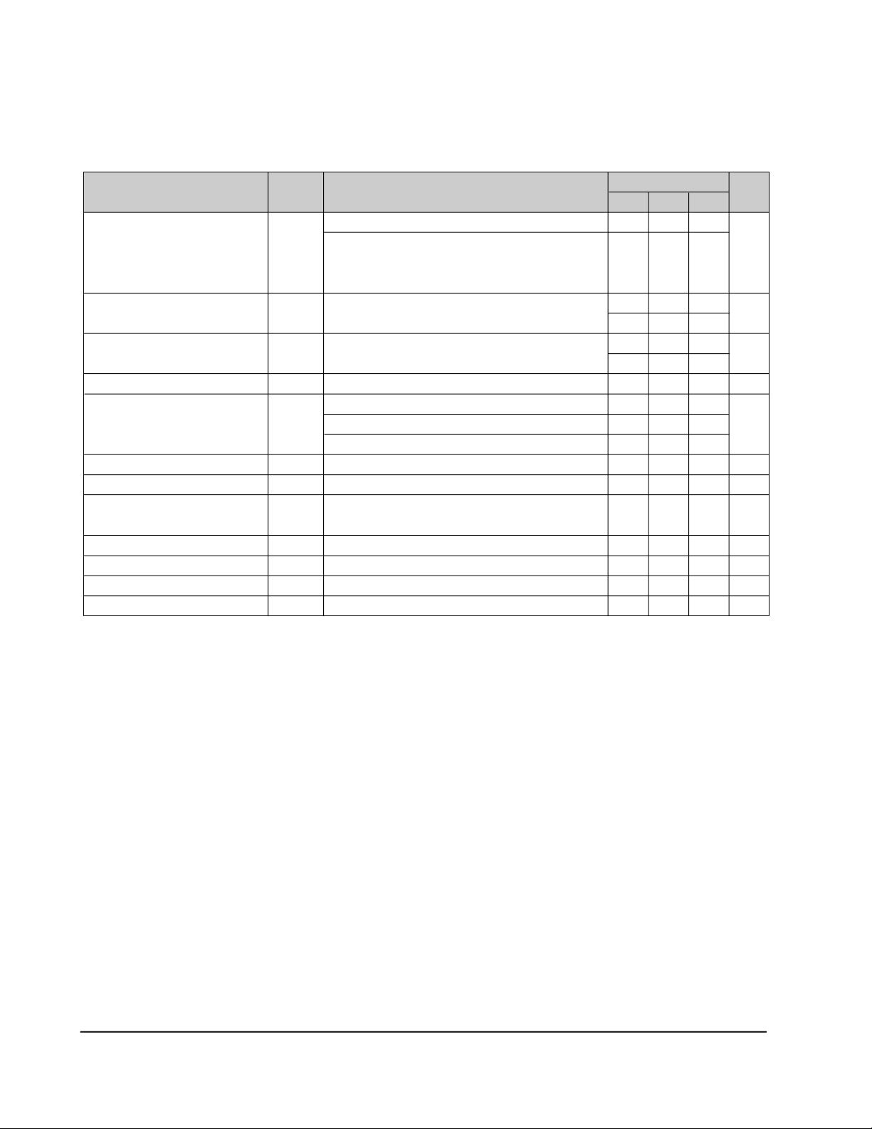
15. Main components specifications
1) REGULATOR
3-TERMINAL 1A POSITIVE VOLTAGE GRGULATORS
The MC78XX/MC78XXA series of three-terminal positive regulators are available in
the TO-220 package and with several fixed output voltaes, making it useful in a
wide range of applicationes. These regulaators can provide local oncard regulation,
eliminating the distribution problems assciated with single point regulation. Each
type employs internal current limiting, thermal shut-down and safe area protection,
making it essentially indestructible. If adequate heat sinking is provided, they can
delive over aA output corrent. Although designed primarily as fixed voltage
regulators, these devices can be used with external components to obtain
adjustable voltages and currents. MC78XXI is characterized for operation from -40°
°Cto +125°c, and MC78XXC from 0°c to +125°c
TO-220 1 2 3 1 : Input 2 : GND 3 : Output
FEATURES
• UOutput Current up to 1.5A
• UOutput voltages of 5;6;8;9;10;11;12;15;18;24V
• UThermal Overload Protection
• UShort Circuit Protection
• UOutput Transistor SOA Protection
• UNo external components required
• UOutput current in excess of 1A
• UIndustrial and commercial temperature range
BLOCK DIAGRAM
ORDERING INFORMATION
Device
Device
MC78XXCT
MC78XXCT
MC78XXACT
MC78XXACT
MC78XXT
MC78XXT
Package
TO-220
TO-220
TO-220
Operating Temperature
0~+125°C
-40~+125°C
ABSOLUTE MAXIMUM RATINGS
Characteristic
Input Voltage (for Vo = 5V to 18V)
(for Vo = 24V)
Thermal Resistance Junction - Cases
Thermal Resistance Junction - Air
Operating Temperature Range MC78XXC/AC
MC78XXI
Storage Temperature Range
Symbol
VIN
VIN
θJC
θ♣JA
Topr
Tstg
Rating
35
40
5
65
0 ~ +125
-40 ~ +125
-65 ~ +150
Unit
V
V
°C/W
θ/W
°C
°C
°C
Samsung Electronics 59
Page 2
2) REGULATOR(MC7812C)
ELECTRICAL CHARACTERISTICS MC7812
(Refer to test circuit, Tmin < Ti < Tmax, Vi = 500mA, Vi = 19V, Ci = 0.33µF, Co = 1.0µFunless otherwise specified)
Characteristic
Output Voltage
Line Regulation
Load Regulation
Quiescent Current
Quiescent Current Change
Output Voltage Drift
Output Noise Boltage
Ripple
Rejection
Dropout Voltage
Output Resistance
Short Circuit Current
Peak Current
Symbol
Vo
∆Vo
∆Vo
Id
∆Id
∆Vo/∆T
Vn
RR
VD
RO
ISC
Ipeak
Ti = 25°C
Ti = 25°C
Test Conditions
Ti = 25°C
5.0mA≤Io≤1.0A, P≤15W
Vin = 14.5V to 27V
Vi = 15.5V to 27V
Vi = 14.5V to 30V
Vi = 16V to 22V
Io = 5.0mA to 1.5V
Io = 250mA to 750mA
Ti = 25°C
Io = 5mA to 1.0A
Vi = 14.5V to 30V
Vi = 15V to 30V
Io = 5mA
f = 10Hz to 100KHz Ti = 25°C
fF = 120Hz
Vi = 15 to 25V
Io = 1A, Ti = 25°C
f = 1KHz
Vi = 35V, Ti = 25°C
Ti = 25°C
Min
11.5
11.4
55
MC7805C
Typ
12
12
10
3.0
12
4.0
5.1
-1
75
71
2
18
250
2.2
Max
12.5
12.6
240
120
240
120
8
0.5
1.0
Unit
V
mV
mV
mA
mA
mV/°C
µ/V
dB
V
mΩ
mA
A
* Tmin < Ti < Tmax
MC78XXI : Tmin = -40°C, Tmax = 125C
MC78XXC, Tmin = 0°C, Tmax = 125°C
* Load and line regulation are specified at constant junction temperature. Changes in Vo due to heating effects must be taken into
account separately. Pulse testint with low duty is used.
60 Samsung Electronics
Page 3

MC 7805 AC(T)
ELECTRICAL CHARACTERISTICS MC7805
(Refer to test circuit, Tmin < Ti < Tmax, Io = 500mA, Vi = 10V, Ci = 0.33ßfi, unless otherwise specified)
Characteristic
Output Voltage
Line Regulation
Load Regulation
Quiescent Current
Quiescent Current Change
Output Voltage Drift
Output Noise Boltage
Ripple
Rejection
Dropout Voltage
Output Resistance
Short Circuit Current
Peak Current
Symbol
Vo
∆Vo
∆Vo
Id
∆‚Id
∆Vo/∆T
Vn
RR
VD
RO
ISC
Ipeak
Ti = 25°C
Ti = 25°C
Test Conditions
Ti = 25°C
5.0mA ≤ Io ≤ 1.0A, Po ≤ 15W
Vi = 7V to 20V
Vi = 8V to 20V
Vi = 7V to 25V
Vi = 8V to 12V
Io = 5.0mA to 1.5V
Io = 250mA to 750mA
˚C
Ti = 25
Io = 5mA to 1.0A
Vi = 7V to 25V
Vi = 8V to 25V
Io = 5mA
f = 10Hz to 100KHz Ti = 25
F = 120Hz
Vi = 8 to 18V
Io = 1A, Ti = 25
f = 1KHz
Vi = 35V, Ti = 25
Ti = 25
˚C
˚C
˚C
˚C
Min
4.8
4.75
62
MC7805C
Typ
5.0
5.0
5.0
1.5
9
3
5.0
-0.8
40
78
2
17
250
2.2
Max
5.2
5.25
100
50
100
50
8
0.5
1.3
U n i t
V
m V
m V
m A
m A
m V / ° C
µ / V
d B
V
mΩ
m A
A
* Tmin < Ti < Tmax
MC78XXI : Tmin = -40˚C, Tmax = 125
MC78XXC, Tmin = 0˚C, Tmax = 125
* Load and line regulation are specified at constant junction temperature. Changes in Vo due to heating effects must be taken into
account separately. Pulse testint with low duty is used.
˚C
˚C
Samsung Electronics 61
Page 4

HIGH-VOLTAGE, HIGH-CURRENT
SOURCE DRIVERS
Series UDS2980H and UDS2980R hermetically sealed source
drivers link standard low-power digital logic and relays, solenoids,
magnetic print hammers, stepping motors, LEDs, and lamps in
applications requiring separate logic and load grounds, load supply
voltages to +80V, and load currents to 500 mA.
Types UDS2981H/R and UDS2983H/R are intended for use
with 5v logic systems(TTL, Schottky TTL. DTL and 5V CMOS).
UDS2982H/R and UDS2984H/R integrated circuits are intended for
MOS interface (PMOS and CMOS) operating from supply voltages
of from 6 to 16V.
Types UDS2981H/R and UDS2982H/R will withstand an output
OFF voltage of 50 V. UDS2983H/R and UDS2984H/R drivers will
withstand a maximum output OFF voltage of 80V.
Under normal operating conditions, the devices will sustain 50
mA continuously on each of the eight outputs at an ambient
temperature of +85°c and with a supply voltage of 15V. All types
include input current-limiting resistors and output transientsuppression diodes. In all cases, outputs are swiched ON by an
active high input level.
Note that the maximum current rating may not be obtained at 55°c because of reduced beta, or at +125°c because of package
power limitations.
Dwg No A 10243
ABSOLUTE MAXIMUM RATINGS
at +25°c Free-Air Temperature
Cutput Voltage Range, VCE
(UDS298t and
UDS2982H/R).......................................5V to 50V
(UDS2983 and
UDS2984H/R).....................................35V to 80V
Input Voltage, Vin
(UDS2981 and
UDS2983H/R).................................................15V
(UDS2982 and
UDS2984H/R).................................................30V
Output Current, Iout-........................................500 mA
Ground Terminal Current,
IGND........................................................................................................3.0A
Power Dissipation. PD
(any one driver).............................................1.1W
(total package).....................................See Graph
Operating Temperature Range,
TA.............................................................................-55˚Cto + 125
Storage Temperature Range,
Ts............................................................................-65˚Cto + 150
˚C
˚C
Series UDS2980H drivers are furnished in 18-pin
ceramic/metal(side-brazed) hermetic dual in-line packages. Series
UDS2980R drivers are supplied in ceramic/glass(cer-DIP) hermetic
packages. Both are processed to the requirements of MIL-STD-883.
Class B.
The same circuits are also available in 18-pin plastic dual in-line
packages (Series UDN2980A) for operation over a limited
temperature range, or where higher package power dissipation is
needes.
FEATURES
• TTL, DTL, PMOS, or CMOS Compatible Inputs
• 500 mA Output Source Current Capability
• Transient-Protected Outputs
• High-Reliability Screening to MIL-STD-883, Class B
• Operating Temperature -55°c to+125°c
Always order by complete part number, e.g.,
See table on next page for differences between devices.
UDS2981H883
62 Samsung Electronics
Page 5

ELECTRICAL CHARACTERISTICS from -55°c to +125°c (unless otherwise specified).
Applicable
Chracteristic
Maximum Output
Leakage Current
Maximum
Collector-Emitter
Saturain Voltage
Maximum
Input Current
Maximum Output
Source Current
Maximum
Supply Current
(Outputs Open)
Maximum Turn-ON
Delay Time
Maximum Turn-OFF
Delay Time
Maximum Clamp Diode
Leakage Current
Maximum Clamp Diode
Forward Voltage
Symbol
ICEX
VCE(SAT)
IIN(ON)
IIN(OFF)
IOUT
IS
tPHL
tPHL
IR
VF
Devices
UDS2981/82
UDS2981/84
UDS2981/83
UDS2982/84
ALL
UDS2981/82
UDS2983/84
UDS2981/83
UDS2982/84
UDS2981
UDS2982
UDS2983
UDS2984
UDS2981/82
UDS2983/84
UDS2981/82
UDS2983/84
UDS2981/82
UDS2983/84
ALL
Temp.
˚C
-55
˚C
+25
+ 1 2 5
˚C
-55
˚C
+25
+125
+25
+25
+25
Test Conditions
VIN = 0.25 V, VS = 50 V
VIN = 0.25V, VS = 80 V
VIN = 2.4 V, IOUT = -100 mA
VIN = 2.4 V, IOUT = -200 mA
VIN = 2.4 V, IOUT = -350 mA
˚ C
˚ C
˚ C
˚ C
˚ C
VIN = 2.4 V, IOUT = -100 mA
VIN = 2.4 V, IOUT = -200 mA
VIN = 5.0 V, IOUT = -100 mA
VIN = 5.0 V, IOUT = -200 mA
VIN = 5.0 V, IOUT = -350 mA
VIN = 5.0 V, IOUT = -100 mA
VIN = 5.0 V, IOUT = -200 mA
VIN = 2.4 V
VIN = 3.85 V
VIN = 12 V
VIN = 0 V, VS = 50 V
VIN = 0 V, VS = 80 V
VIN = 2.4 V, VCE = 2.2 V
VIN = 5.0 V, VCE = 2.2 V
VIN = 2.4 V, VS = 50 V
VIN = 5.0 V, VS = 50 V
VIN = 2.4 V, VS = 80 V
VIN = 5.0 V, VS = 80 V
VS = 35 V, RL = 175 Ω
VS = 50 V, RL = 250 Ω
VS = 35 V, RL = 175 Ω
VS = 50 V, RL = 250 Ω
VIN = 0.25 V, VS = 50 V
VIN = 0.25 V, VS = 80 V
IF = 200 mA
Fig.
1
1
2
2
2
2
2
2
2
2
2
2
3
3
3
3
3
2
2
4
4
4
4
7
7
7
7
5
5
6
Limit
200 µA
200 µA
2.0 V
2.1 V
2.0 V
1.8 V
1.9 V
2.0 V
2.1 V
2.0 V
1.8 V
1.9 V
295 µA
600 µA
2.3 mA
10 µA
10 µA
-200 mA
-200 mA
10 mA
10 mA
10 mA
10 mA
2.0 µs
2.0 µs
10 µs
10 µs
50 µA
50 µA
1.75 V
*All inputs simultaneously.
**Pused test.
*Complete part number includes a terminal letter that indicates package (H = ceramic/metal side-brazed. R = ceramic/glass cer-DIP).
Samsung Electronics 63
Page 6

KSR1005 NPN EPITAXIAL SILICON TRANSISTOR
SWITCHING APPLICATION (Bias Resistor Built In)
•Switching Circuit, Inverter, Interface circuit Driver circuit.
•Built in bias Resistor (R,=4.7KΩ, R=10KΩ)
•Complement to KSR2005
ABSOLUTE MAXIMUM RATINGS (Ta=25˚c)
Characteristic
Collector-Base Voltage
Collector-Emitter Voltage
Emitter-Base Voltage
Collector Current
Collector Dissipation
Junction Temperature
Storage Temperature
Symbol
VCBO
VCBO
VCBO
IC
PC
TI
Tstg
Rating
50
50
10
100
300
150
-55-150
ELECTRICAL CHARACTERISTICS (Ta=25˚C)
Characteristic
Collector-Base Breakdown Voltage
Collector-Emitter Breakdown Voltage
Collector Cutoff Current
DC Current Gain
Collector-Emitter Saturation Voltage
Output Capacitance
Current Gain-Bandwidth Product
Input Off Voltage
Input On Voltage
Input Resistor
Resistor Ratio
Symbol
BVCBO
BVCBO
ICBO
HC
VCE(sat)
Cob
Fr
Vi(off)
Vi(off)
R1
R1/R2
Test Condition
IC=10µA, IB=0
IC=100µA, IB=0
VCB=40V, IB=0
VCB=5V, IB=5mA
IC=10mA, IB=0.5mA
VCB=10V, IB=0
t=1MHz
VCB=10V, IC=5mA
VCB=5V, IC=100µA
VCB=0.3V, IC=20mA
Unit
V
V
V
mA
mW
˚C
˚C
Main
50
50
30
0.3
3.2
0.42
TO-92
1 Emitter 2 Collector 3 Base
Typ
3.7
250
4.7
0.47
Max
0.1
0.3
2.5
6.2
0.52
Unit
V
V
µA
V
pF
MHz
V
V
KΩ
Equivalent Circuit
64 Samsung Electronics
 Loading...