

Page 1

SF700AT 5-1
5. Circuit Description
5-1 General
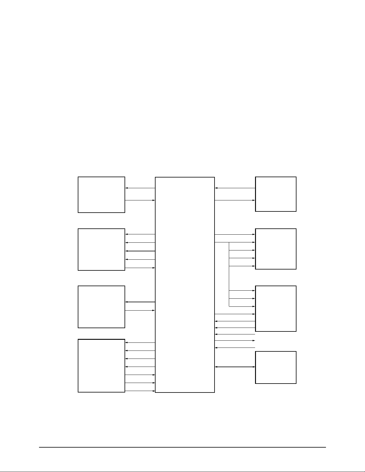
The main circuit board consists of memory, MODEM, TX- and RX-related circuitry, Speakerphone, TAD,
and the Integrated Facsimile Controller (IFC), which includes the CPU and I/O device drivers and controls
the system.
5-2 IFC
This circuit consists of the data and address bus, real time clock (RTC), image sensor, motor driver
controller, Thermal Print head controller, IFC including I/O port, and system reset circuit.
Figure 5-1: XFC-B Memory Map
CPU (Logical) Address Space
FFFFFF
F00000
0FFFFF
000000
MCSn
ROMCSn
CS0n
Not
Available
Internal
Registers
CS2n CS4n
CS1n
Internal
Memory
00FFFF
00FF00
00FE00
00FD00
00FC00
00E000
Reserved
Setup
Registers
Operational
Registers
CS4n
CS3n
CS2n
Reserved
Shading Inversion
DBCMC Buffer
Dither Table
Reserved
00FEFF
00FEE0
00FE80
00FE00
00FDFF
00FDC0
00FD80
00FD00
00FBFF
00FBE0
00FBD0
00FBC0
00FB80
00E000
5-2-1 Memory Map
The external memory of the CPU is divided into
32kB RAM (0000H through 8000H) and 64kB ROM
(FF0000H through FFFFFFH).
Page 2
Circuit Description
5-2 SF700AT
Figure 5-2: XFC-B Hardware Interface Signals
5-2-2 Data & Address Bus Control
/RD and /WR signals are active in the low state,
with the PH2 clock in a high state, and an internal
wait state occurs in the TSTCLK (6 MHz). These
signals are sent to the /RD and /WR ports of
RAM , ROM, and the MODEM in order to read or
write data when a chip select line is active.
/CS0: RAM chip select active (low)
/ROMCS: ROM chip select active (low)
/MCS: MODEM chip select active (low)
D0 - D7: 8 bit data bus
A0 - A16: address bus
5-2-3 System Clock
The 6 MHz internal clock frequency is generated
by dividing the 12 MHz system clock from
MODEM by two inside the MODEM.
OPERATOR
PANEL
SERIAL
COMMUNICATION
PRINTER
DATA
CONTROL
AND
SENSORS
MOTOR
DRIVER
(MOTOR)
SCANNER
CONTROL
AND
PROCESSING
RTC
CRYSTAL
EXTERNAL
BUS
MODEM
GENERAL
PURPOSE
I/ 0
TXD
RXD
STB 0~3
PDAT
PCLK
PLAT
THADI
SM 0~3
MOTOR POS
START
SCLK
VIDCTL1
H/B
Vin
+Vref
-Vref
XIN
XOUT
/ROMCS
/RAMCS
/RD/WR
D0~D7
A0~A16
/RD/WR
D0~D7
A0~A4
/MCS
/MIRQ
SYSCLK
/PWRDWN
/RESET
/BATRST
IFC(XFC-B)
Page 3

Circuit Description
SF700AT 5-3
Figure 5-4: Printer Timing
5-2-4 Real Time Clock (RTC)
This circuit receives clock pulses from an external
32.768 kHz crystal, which it divides into hours,
minutes, seconds, year, month, and day.
A battery maintains operation when power is off.
XFC-B can up-track 32 years, beginning with 1992.
5-2-5 Print Control
The PCLK and PDAT signals synchronise serial
print data to the TPH. PLAT latches TPH serial
print data to the TPH from a shift register through
PDAT. STB0 - STB3 enable TPH printing in four
sequential intervals.
This system has 10ms/Line printing format and
determines STB High/Low enable status
according to the STBPOL signal.
Figure 5-3: RTC Block Diagram
32768 KHz
15 BIT
PRESCALER
1Hz CO=60 CO=60 CO=24
6 BIT
SECONDS
6 BIT
MINUTES
5 BIT
HOURS
BUSY
DETECT
5 BIT
DAYS
4 BIT
MONTHS
5 BIT
YEARS
MONTH
DECODER
LEAP YEAR
DECODER
3 STATE
DRIVER
BUSY FLAG CLEAR BUSY FLAG
CO=28,29,
30,or 31
CO=12
PrintLine
(MSINT Cary-out)
Shift Data
Sh D Sh C Sh D Sh C
Print
Cmd
Shift Clk
STB0
STB1
STB2
2 DotClk Delays
5 DotClk Delays
2 DotClk Delays
STB3
Print
Cmd
Page 4
Circuit Description
5-4 SF700AT
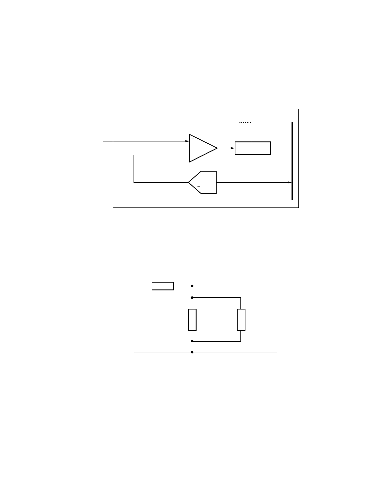
5-2-6 TPH A/D Converter
The TADC is composed of a 6 bit DAC,
comparator, filter, and 9 bit up/down counter. The
6 MSBs of the 9 bit counter generate a reference
signal to the comparator. TPH temperature is
sensed by comparing DAC output voltage to the
comparator with the thermistor
input voltage (THDI), which originates as an
output signal from the TPH. It then supplies the
proper strobe pulse to the TPH. The thermistor
input voltage (THDI) operates within a range of 1
to 4V.
Figure 5-5: Thermal ADC Block Diagram
Figure 5-6: THDI/Thermal Printer Head Connection Circuit
+5V
Ground
R28
R29
THD1
Rt (T)
Thermal
printhead
thermistor
Approximate values of R28 and R29 can be calculated
from the following formulas:
R28=0.25*[R29*rT(T1)]/[R29+Rt(T1)]
R29=[15Rt(T1)*Rt(T2)]/[Rt(T1)-16Rt(T2)]
where T1=minimum temperature, T2=maximum temperature.
THDI
DAC out
Comparator
+
6-bit DAC
1/2 bit
+
6 MSBs
9-bit up/down
Counter
Counter Clock
Data Bus
Page 5
Circuit Description
SF700AT 5-5
SclkCtrlLo
SclkCtrlHi
Band Gen (8x)
Tx/Rx Control
IRQ control
SARTCmd RxShift Reg
SartlRQ
CPU Bus
SCLK
RXD
TXD
Internal Register
(SARTData)
RxBuffer
(SARTData)
TxShift Reg
5-2-7 Operation Panel Control
Communication
A Synchronous/Asynchronous
Receiver/Transmitter (SART) controls serial data
transmission between the main circuit and the
operator panel.
Figure 5-7: SART Block Diagram
Page 6

Circuit Description
5-6 SF700AT
5-2-8 Image Sensor
The shading wave is formed by scanning the white
roller prior to a document. The slice level is
determined by the shading wave, and
compensates for shading distortion according to
the CIS characteristics. The wave format from the
CIS is converted into a 6 bit digital value in the IFC
image processor, and then processed in B/W or
intermediate mode.
Shading Correction
Inversion
Table
8x6
Mutiplier
8
8
4
1
2
Shade RAM
8
8
External
Video
Processing
Data Output
Text mode image
Dynamic
Background &
Contrast Control
1
External
Video
Processing
Data Input
To Line
Buffer IF
(DMA Channel 1)
4
1
1
6
8
FADC
Gray Scale Image
Edge
enhancement
3
Dithering
or B/W
Thresholding
Dither
Table
Scan Data
Bi-level
B4 to A4
Reduction
Primary Paths
Secondary (optional) Paths
Inversion Table Enabled (ShTblEnb)
Edge Enhancement Enabled (EdgeEnhEnb)
Dynamic Background and Contrast Control
Enabled (DBCCEnb)
Shading Enabled (ShadeEnb)
1
2
3
4
Figure 5-8: Scanner Image Processing Block Diagram
Page 7

Circuit Description
SF700AT 5-7
Figure 5-10: CIS Driver Clock Timing
5-2-10 CIS Driver
The CIS driver clock frequency is 500 kHz. A low
duty cycle of 50% is used to lengthen the charging
time. A start signal is provided every 5 ms to
match the line scanning time. Actual image signal
is provided in less than 4.1 ms, using the 500 kHz
clock and taking B4 paper size into consideration.
500 KHZ (L:DUTY 50 %)
SI
CLOCK
SIG
1 LINE
Figure 5-9: Scanner Interface Block Diagram
5-2-9 CIS Input Processor
To process the B/W input signal, maximum
(+V
REF
) and minimum (-V
REF
) values of the CIS
input signal are controlled by calibrating MUXA
and MUXB in the high state for the maximum
level, and setting them to earth for the minimum
level.
Processing to compensate for CIS shading
distortion is controlled with MUXA 'low' and
MUXB 'high'. For B/W mode, MUXA should be
'high', and MUXB 'low'. For half-tone, MUXA is
'low', and MUXB is 'high'.
XFC-B External Circuits
Dither & Shading
Correction
Tables
Scanner Image
Processing
Shading RAM
External
RAM
Line Buffer
RAM
6-bit FADC
Video
Processing
-Vref
+Vref
+
-
Vin
Scanner
VIDCTL(1:0)
Drivers
Start, CLK1.
CLK1n, CLK2
Scanner
Timing & Control
CPUCLK
Page 8

SPEAKER DISABLE
SPEAKER ENABLE
-
A4 Detect
-
B4 Detect
-
Document Scan Position Detect.
-
D6365A ACKNOWLEDGE
MODEM TX Path
CODEC TX Path
B4 Paper detect
B4 Paper empty
A4 Paper detect
A4 Paper empty
Cutter Off
Cutter On
Cutter Forward
Cutter Reverse
-
Cutter Position Detect
High Byte Select
Low Byte Select
OPE UART TX
OPE UART RX
Ring Not detection
Ring detection
DATA PUMP Disable
DATA PUMP Enable
RX Motor Phase A ON
RX Motor Phase A OFF
RX Motor Phase B ON
RX Motor Phase B OFF
RX Motor Phase -A ON
RX Motor Phase -A OFF
RX Motor Phase -B ON
RX Motor Phase -B OFF
Circuit Description
5-8 SF700AT
5-2-11 I/O Port Table
CIRCUIT NAME
I/OPIN NO PIN NAME
STATE
DESCRIPTION
/SPK CTL
A4_DET
/B4_DET
/DSCAN
/DSP_ACK
TX_CTRL
/B4_EMP
/A4_EMP
/CUT_EN
CUT_PH
CUT_POS
/DSP_H/L
TXD
RXD
/RING_DET
/DATA FLAG
PMA
PMB
/PMA
/PMB
GPIO 0
GPIO 1
GPIO 2
GPIO 3
GPIO 4
GPIO 5
GPIO 6
GPIO 7
GPIO 8
GPIO 9
GPIO 10
GPIO 12
GPIO 13
GPIO 14
GPIO 16
GPIO 17
GP00/PM0
GP01/PM1
GP02.PM2
GP03/PM3
(ONLY 0)
O
I
I
I
I
O
I
I
O
O
I
O
-
I
I
O
O
O
O
H
L
H
L
H
L
H
L
H
L
H
L
H
L
H
L
H
L
H
L
H
L
H
L
H
L
H
L
H
L
H
L
H
L
H
L
H
L
94
93
92
91
90
89
87
86
85
84
83
80
79
78
76
75
118
117
116
115
Page 9

Circuit Description
SF700AT 5-9
5-2-12 Motor Controller
This facsimile machine perform sending,
receiving, and printing functions utilising a two 24
volt motor. These motor has a winding resistance
of 120 ohm.
5-2-13 Miscellaneous Signals
The key click consists of an 800 Hz tone of 20 ms
duration.
/RESET drives MODEM /POIR and serves to
reset the MODEM.
/MIRQ is the MODEM interrupt signal.
TX Motor Phase A ON
TX Motor Phase A OFF
TX Motor Phase B ON
TX Motor Phase B OFF
TX Motor Phase -A ON
TX Motor Phase -A OFF
TX Motor Phase -B ON
TX Motor Phase -B OFF
RESERVED
RESERVED
RESERVED
CIRCUIT NAME
I/OPIN NO PIN NAME
STATE
DESCRIPTION
SMA
SMB
/SMA
/SMB
N.C.
N.C.
N.C.
SM0
SM1
SM2
SM3
D0/Q0
D1/Q1
D2/Q2
O
O
O
O
O
O
O
H
L
H
L
H
L
H
L
-
-
-
106
105
104
103
2
5
6
Page 10

Circuit Description
5-10 SF700AT
POWER MONITOR
If 5V power to KIA7045F drops to between 4.65
and 4.35V (typically 4.5V), power failure will be
indicated and the output of KIA7045F will go 'low'
(GND). This causes the IFC to become active
('low'=reset). The IFC reset causes the MODEM
IFC/RESET terminal to be reset. The output
terminal of KIA7045F is an open-drain
configuration, and is connected to PFC through a
10k pull-up resistor.
WATCH DOG TIMER
This programmable counter in the IFC is reset
every 2 ms. If not reset after 250 ms, the system is
automatically reset and switches to initialise mode.
BATTERY POWER RESET
When battery power (VB) is applied to IFC the first
time, VB current results in /BATRST going 'low',
causing a reset to occur.
5-2-14 Reset
Two power resets and a watchdog timer in the IFC
comprise the elements of this circuit. Battery
power reset (/BATRST) is used to initialise the
battery-powered logic, and primary power reset
(/PWRDWN) initialises non-battery-powered
logic when system power is supplied.
Figure 5-12: Power Reset Block Diagram
icik (TSTCLK)
Watchdog Reset
Reset clock
reset
Divider
XOUT
/PWRDWN
Power
Down
NMI
Power up Delay 1
(1-2 Reset clocks)
Power up Delay 2
(8 TSTCLKS)
vddresn
RESETn
resn
To internal logic
Clock enable
MC24 NMI
routine
set
lock
clear
Lockout
Logic
lockout
to battery (BackupConfig) register reset
BATRSTn
set tristate
Tristate
Control
CS0n
Page 11

Circuit Description
SF700AT 5-11
5-3 Memory
System memory consists of 128kB ROM and 32kB RAM. All of RAM is backed up. ROM and RAM are
selected by chip select lines, and data is accessed by the units position of the byte.
+5V power is applied to RAM through VB. This model facsimile machine uses a Li battery. A 1k resistor in
series with the positive battery terminal is for battery protection.
5-4 Modem and TX- and RX- Related Circuits
These circuits control signal transmission between the internal MODEM and the LIU or a remote MODEM.
The R96DFXL MODEM is a single-chip fax-MODEM having features to detect and generate DTMF tones.
TX OUT is the MODEM output port, and RX IN is the input port. /PORI is the IFC signal which enables
MODEM initialisation at system power on. D0 - D7 are data buses. RS0- RS4 are internal register select
signals which determine the mode. /MCS is the chip select signal, and /RD. /WR. are the read and write
control signals. RLSD is used for v.24 interface-related signals and /IRQ is the MODEM interrupt.
Refer to Figure 5-14 for available R96DFXL I/O ports.
Table 5-14: I/O Port
HALFTONE MODE
BINARY MODE
-
-
-
OPE RESET ENABLE
CML1 ON
CML1 OFF
BREAK
MAKE
+24V ON
+24V OFF
CIS LED ON
CIS LED OFF
-
PAPER JAM
DP DIALING MODE
DTMF DIALING MODE
-
CIRCUIT NAME
I/OPIN NO PIN NAME
STATE
DESCRIPTION
HT/_BINARY
GND
/OPE RESET
CML1_ON
/DP_ON
+24V_ON
GLED_ON
N.C.
/PJAM
GND
DIAL_MODE_IN
N.C.
N.C.
GP 02
GP 03
GP 04
GP 05
GP 06
GP 07
GP 11
GP 13
GP 16
(ONLY I)
GP 17
(ONLY I)
GP 19
(ONLY I)
GP 20
(ONLY I)
GP 21
(ONLY I)
O
O
O
O
O
O
O
O
I
I
I
I
I
H
L
H
L
H
L
H
L
H
L
H
L
H
L
-
H
L
H
L
H
L
-
-
100
1
2
3
4
5
63
61
75
76
94
93
91
Page 12

Circuit Description
5-12 SF700AT
5-4-1 Transmit Circuit
This circuitry controls transmission of analog
signals from the MODEM. Output voltage from
the MODEM is buffered through the LIU board
and OP amp after signal smoothing and filtering,
and finally output to the line.
5-4-2 Receive Circuit
In receive mode, analog signals from the LIU
board are transferred to RX IN through the BPF
and smoothing filter.
5-5-1 Transmit Path
Voice signal from the condenser microphone is
amplified through OP Amp(U2) in the OPE PBA.
This signal is received CODEC1(U22) through
LPF. LPF (Low Pass Filter) consisting of R100 and
C95 is an anti-aliasing filter to clear the aliasing
noise occuring while sampling the signal. Q9 and
Q11 compose ALC (Automataic Limit Controller)
circuit. CODEC 1 (U22) converts the voice signal
from microphone into digital and CODEC 0 (U24)
converts the digital signal from voice coprocessor
into analog to emit it to line output.
5-5-2 Receive Path
CODEC 0 converts the voice signal from line into
digital and sends it to DSPG. CODEC 1 converts
the digital output from DSPG into analog signal
and sends it to analog MUX (U12 ). The signal is
amplified by Audio amp and sent to Speaker.
5-5-3 Mic Input Path
Transmit path functions as MIC input path.
Outgoing messages and memo messages out from
CODEC 1 are stored in the voice memory (U21)
through the DSPG DRAM controller.
5-5-4 Line Input and Play Path
Incoming signal from line are stored in the voice
memory (U21) through CODEC 0 (U24) and DSPG
DRAM controller. When it is played, DSPG
processes the data stored in the voice memory and
sends them out to LIU through CODEC 0 and
R146. To playback through the speaker, DSPG
sends them out to speaker through R108, MUX
(U12), and OP amp(U16).
5-5-5 DSPG
This circuit consists of Host Interface, Memory
Interface, CODEC Interface, Speakerphone
Processor, and DSP core. Host Interface sends and
receives data to and from IFC. Memory Interface
sends and receives the compressed voice data to
and from DRAM (or EPROM) to play back and
record voice data. Speakerphone processor
controls TX and RX path, and is connected to line
and the user through CODEC interface. DSP core
communicates with host IFC through Host
Interface.
5-5-6 Voice Backup
+5V is supplied for the voice memory through
VBT when power is on. When power is off, +5V is
supplied from the battery. 9V Lithum battery is
used for backup battery.
5-5 Speakerphone and TAD
Speakerphone circuit consists of transmit path, receive path, and voice coprocessor (D6365A) to convert the
transmit path and receive path. TAD circuit consists of voice coprocessor to record and play voice messages
and voice memory.
Page 13

Circuit Description
SF700AT 5-13
5-6 LIU PBA
The LIU (Line Interface Unit) interfaces the MODEM and telephone to the telephone line. The FAX and
telephone portions of the LIU are active with machine power on. When machine power is off, only the
telephone circuitry operates, powered by telephone line voltage. The FAX portion of LIU consists of the
interface between MODEM and telephone line, and the circuits for DC loop feeding, DP signal, Loop
Current, and Ring Detect. The telephone portion is divided into ringer, dialing, and speech circuits. Refer to
the Schemetic and Wiring Diagram sections of this manual.
5-6-1 FAX section
MODEM/ LINE INTERFACE
This is the path for data and remote control
signals.
¥ CML1 relay: switches telephone line between
FAX and telephone circuits.
¥ T1: impedance matching between line and LIU
FAX circuity.
¥ C40: DC blocking for T1.
RING DETECT
Ringer IC U1 pin 1 is output port. This signal is
applied to photo coupler for ring detection.
DP SIGNAL CIRCUIT (DC)
Determines the DC characteristics of the interface
circuitry when the FAX section is on-line. The dial
pulse (DP) is generated by interrupting DC line
loop with the Photo coupler IC, K2.
¥ BD2: telephone line polarity matching
¥ VAR2, 3: 82V voltage regulator
¥ R44, R45: Vgs bias voltage regulator
¥ C39: voltage stabilization
¥ R46: DC resistance adjustment.
¥ K2: dial pulse generator
LOOP CURRENT DETECT
This circuit is required to enable AGC function in
speakerphone mode. When CML 1 relay switches
to FAX, U7 (PC814A) in the LIU board converts
the loop current between tip and ring to voltage
value and apply it to the pin 15 of U26 (4052) in
the main board.
The line loop current voltage will be adjusted to
1V - 4V in the LIU board. R54 performs this
function. Variable resistor VR1 is used to
compensate a deviation of photo coupler.
AGC circuit amplifies voice signal gain received
according to the loop current in the main board as
follows:
Loop Current Loop Current Range Gain
39 mA or more 0 dB
38 mA (20) 31-38 mA 2 dB
30 mA (26) 26-30 mA 4 dB
25 mA (31) 21-25 mA 6 dB
20 mA (35) 20 mA or less 8 dB
(This Gain is amplified by U16: 4051 circuit)
Page 14

5-6-2 Telephone Section
RINGER CIRCUIT
¥ U1: MC34012P and associated components.
¥ Line Ring voltage passes through DC blocking
capacitor C4 and attenuator R11 to U1 pins 2
(AC1) and 3 (AC2).
¥ U1 filters the signal and output is pin 4. This is
the PIEZO buzzer drive signal.
¥ Output frequency is determined by C1 and R4
controls threshold voltage.
DIALLING CIRCUIT
¥ U2: KS58503 and associated components.
¥ U2 pin 6 is EARTH.
MF DIAL
¥ U2 pin 7 is set to EARTH by T/P switch (SW2).
¥ MF signal appears at U2 pin 12, then through
R17, R26, C29, R19 is provided U3 pin 13.
¥ Line dial signals appear at U3 pin 1. This point
also provides sidetone audio.
SPEECH CIRCUIT
¥ TEA1067 (U8) and associated components.
¥ Transmitting circuit
¥ Handset dynamic microphone is filtered by
resistors and capacitors and then amplified by
U3 pins 7 and 8 (MIC-, MIC+).
¥ L6 and L7 are RF filtering.
¥ U8 pin 1 (LN) is audio output to telephone line.
PULSE DIALl
¥ U2 pin 7 (Mode) is set to VDD by R20 pullup
resistor.
¥ Dial pulses originate at U2 pin 14, which toggles
MV Q3/Q2, which drives Q4.
¥ Q4 output interrupts the telephone line.
¥ Pulse M/B ratio is set by U2 pin 6.
V
DD=33:66, and VSS=40:60.
¥ Optical coupler U6 inhibits manual dial when
+5V is applied to pin 1 by carthing Q1 base,
driving U2 pin 5 high. This prohibits manual
dialling during FAX auto-dial.
TRANSMITTING CIRCUIT
¥ Handset dynamic microphone is filtered by
resistors and capacitors and then amplified by
U3 pins 7 and 8 (MIC-, MIC+).
¥ L3 and L4 are RF filtering.
¥ U3 pin 1 (LN) is audio output to telephone line.
¥ Transmit audio transfer level control is U3 pins 2
and 3 (GAS1, GAS2) through R48, C36.
RECEIVER CIRCUIT
¥ Receive audio from line is fed to U13 pin 18 (SLPE).
¥ Handset receiver audio is U3 pins 4 and 5 (QR-,
QR+).
¥ R49, C41, C37 are high frequency roll-off.
¥ L5 and L6 are RF filtering.
SIDETONE CIRCUIT
¥ Sidetone audio characteristics are controlled by
R42, R38, C53, C26, C27, C53.
Circuit Description
5-14 SF700AT
Page 15

Circuit Description
SF700AT 5-15
Figure 5-13 OPE Block Diagram
5-7 OPE PBA
OPE PBA consists of U1 (MICOM Z8601), LCD, key matrix, LED indicators, and mic input circuit for
speaker phone and DTAD. Refer to OPE Schematic Diagram and Wiring Diagram sections of this manual.
¥ Signals from the key matrix and delivered to U1 X/Y input pin group (P1-x).
¥ U1 pin 4 (TX DATA) is UART code to MAIN PBA.
¥ Display from controller is received at U1 pin 5 (RX DATA).
¥ LCD drive signals are U1 P20~P27, P33~P35 pins.
¥ Machine status LED drive signals are U1 P00~P02, P04~P06 pins.
mic Input
Circuit
Connector
Main
MICOM
Z-8601
LCD
16 x 1 lines
Key Matrix
LEDs
6
8
2
Y
X
6
11
2
UART
Reset
Page 16

Circuit Description
5-16 SF700AT
MEMO
 Loading...