

Page 1
5. Circuit Description
5-1 Main PBA
5-1-1 Summary
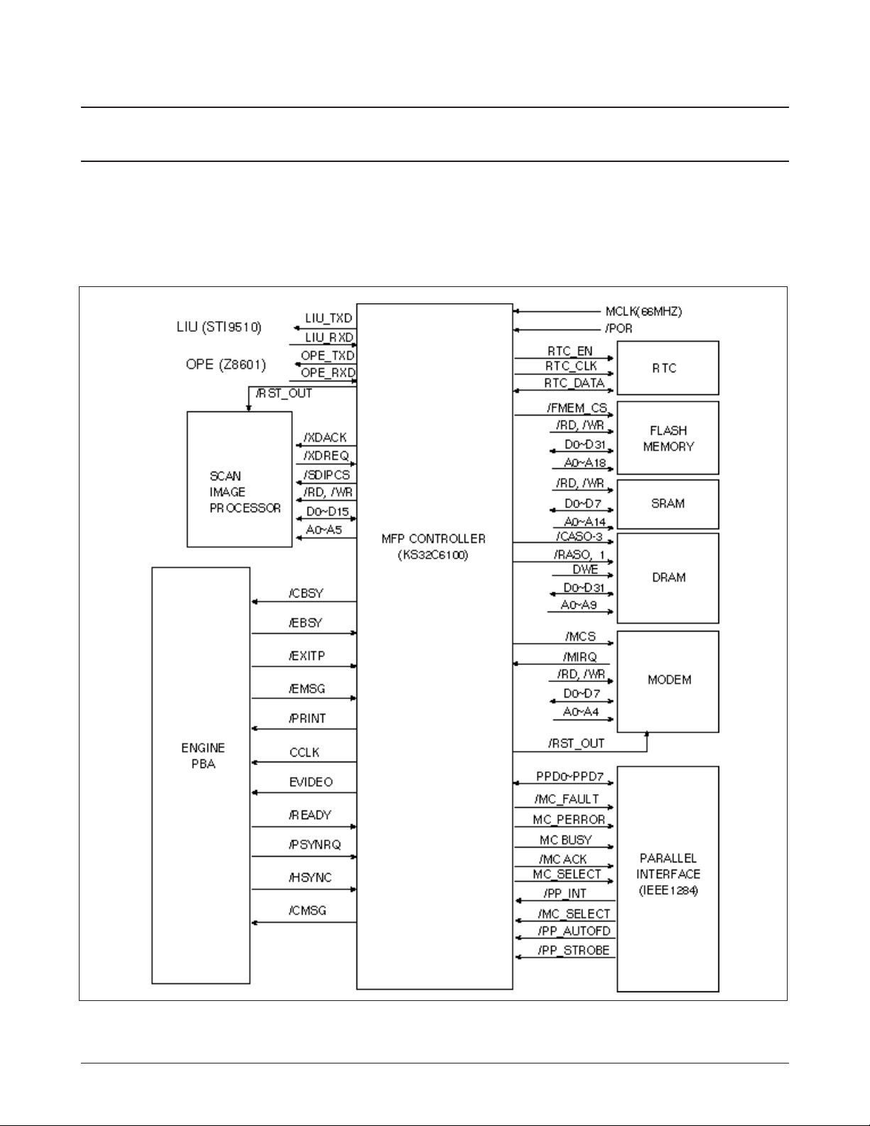
The main circuit that consists of CPU, MFP controller (built-in 32bit RISC pr ocessor cor e : ARM7TDMI)
including various I/O device drivers, system memory, scanner, printer, motor driver, PC I/F, and FA X
transceiver controls the whole system. The entire structure of the main circuit is as follows:
Samsung Electronics 5-1
Fig.5-1. Entire Structure of Main Circuit for Each Key Signal
Page 2

5-2 Samsung Electronics
Circuit Description
5-1-2 MFP Controller (KS32C6100 : U1)
Fig.5-2. Uart Block Diagram
SYSTEM CLOCK
The internal clock frequency is 33MHz 66MHz system
clock (MCLK) supplied from the outside is used being
divided inside.
DATA & ADDRESS BUS CONTROL
• /RD & /FMEM_WR, /WR
/RD & /FMEM_WR signals are synchronized with
MCLK(33MHz) and become LOW ACTIVE.
These signals are strobe signals used to read and
write data when each CHIP SELECT is connected
with /RD and /WR pin of RAM, ROM, MODEM
and the outside devices and becomes active.
/WR is strobe signal used only write signal for
SCAM image processor.
• CHIP SELECT (/SDIP_CS, /RCS0, /RCS2, /MCS,
/SCS
- /SDIP_CS : SCAN MEMORY CHIP SELECT (LOW
ACTIVE)
- /RCS0 : FLASH MEMORY CHIP SELECT (LOW
ACTIVE)
- /RCS2 : MASK ROM CHIP SELECT (LOW
ACTIVE)
- /MCS : MODEM CHIP SELECT (LOW ACTIVE)
- /SCS : SRAM CHIP SELECT (LOW ACTIVE)
• D0 - D31
- 32bit data bus
• A0 - A 2 3
- ADDRESS BUS (A22 - A23 are reserved.)
SERIAL COMMUNICATION PART
U A R T (Universal Asynchronous
Receiver/Transmitter) at KS32C6100 enables the main
and LIU, main and OPE to transmit serial data. The
block diagram of UART i s a s follows:
KS32C6100 has two UART channels. The baud rate is
9600bps.
Page 3

Circuit Description
Samsung Electronics 5-3
Fig.5-3. Uart Data Format
Fig.5-4. External DMA Timing Diagram
EXTERNAL DMA
It brings data fr om an external device (SCAN_IP:U31)
through EXTDMAchannel 1. When the DMA
REQUEST is sent from a n external device to
KS32C6100, DMA ACKNOWLEDGE signal is
activated and DMA channel 1 is driven to produce
CHIP SELECT and READ STROBE (/RD) and data is
br ought fr om the external device. It generates the
address, CHIP SELECT and WRITE STROBE (/WR)
i n o r der to move this data to destination memory, a nd
then stores the data.
In other words, when the external DMA is requested
by an external device, KS32C6100 drives internal
D M A controller, D M A channel 1 is assigned to
external channel, the data is sent from memory to
memory or from external device to memory.
Following timing shows that when DMA REQUEST
(/XDREQ) is generated, DMA ACKNOWLEDGE
(/XDACK) is sent after 2 cycles and the 2 Word Data
is r ead fr om external device, and is written into
memory. After that if the DMA REQUEST is
maintained continuously, DMA ACKNOWLEDGE
signal is generated after 4 cycles and the same
operation is repeated.
Following diagram shows one DMA cycle. The
external device (SCAN_IP) using the DMA maintains
continuously DMA r equest to be activated until
second DMA is performed, so one r equest brings 2
Word.
Page 4

Circuit Description
5-4 Samsung Electronics
DRAM CONTROLLER
As KS32C6100 has DRAM contro ller, DRAM can be
connected with external memory.
The control mode of DRAM controller can access
EARLY WRITE, NORMAL READ, PAGE MODE, and
BYTE/HALF, and supports EDO DRAM as well as
normal DRAM.
DRAM READ/WRITE signals use /DWE signal to
control system buses. It supports CAS BEFORE RAS
for DRAM REFRESH. Connected with common
/CAS(0-3), /RAS(1:0), it consists of 2 banks and each
may be connected with up to 2M - 8M halfword, t h e
default setting of this system is 8MB.
The field of DRAM is in figure 5-1 (Entire Str uctur e of
Main Circuit for Each Key Signal), r elated timing
diagram is in figure 5-4.
R
TC (REAL TIME CLOCK)
R TC circuit maintains curr ent time information, and it
operates in both primary power mode and battery
back-up mode. As RTC does not in MFP contr oller,
R TC IC is needed separately. This cir cuit (R TC-4513)
receives clock source from an internal 32.768 kHz
crystal, and divides it into hours, minutes, seconds,
year, month, and day. RTC_EN, DATA and CLK
control the R TC IC. RTC_EN is CHIP SELECT signal,
DATAis bidirectional signal and used to select mode,
write addre ss, read/write data. CLK reads or output
data in rising edge.
PARALLEL PORT INTERFACE
KS32C6100 has parallel port interface enabling
parallel interface with PC. This part connected with
the computer through the centr onics connector makes
possible parallel interface with the computer. It
generates control signal and consists of /ERROR, PE,
BUSY, /ACK, SLCT, /INIT, /SLCTIN, /AUTOFD,
and /STB.
Data is transmitted according to the standard of IEEE
P1284 (http://www.fapo.com/ieee 1284.html). The
controller supports compatibility mode which is the
traditional way to transmit print data, nibble mode
(4bit data) to upload data to the computer, and ECP
(Extended Capabilities Port: 8bit data transmission)
duplex high-speed transmission with the computer.
Compatibility mode, called as Centronics mode, is
protocol which used to transmit data from PC to
printer. ECP mode is protocol which supports rapid
bidir ectional communication with input/output
device such as printer, scanner. ECP mode supports 2
cycles for bidir ectional communication: Data cycle
and Command cycle. Command cycle is formed runlength count and channel addressing. RLE (Run
Length Encoding) mode can compress data, and be
used to transmit raster image to printer or scanner.
This system uses RLE method for high-speed
transmission. It enables data to be printed, uploaded,
and downloaded. It also monitors system.
Page 5

Circuit Description
Fig.5-5 Compatibility Hardware handshaking Timing
1. Write the data to the data register.
2. Program reads the status register to check that the printer is not BUSY.
3. If not BUSY, then Write to the Control Register to assert the STROBE line.
4. Write to the Control register to de-assert the STROBE line.
Fig.5-6 ECP Hardware Handshaking Timing (forward)
1. The host places data on the data lines and indicates a data cycle by setting nAUTOFD.
2. Host asserts nSTROBE low to indicate valid data.
3. Peripheral acknowledges host by setting BUSY high.
4. Host sets nSTROBE high. This is the edge that should be used to clock the data into the Peripheral.
5. Peripheral sets BUSY low to indicate that it is ready for the next byte.
6. The cycle repeats, but this time it is a command cycle because nAUTOFD is low.
Samsung Electronics 5-5
Page 6

Circuit Description
Fig.5-7 ECP Hardware Handshaking Timing (reverse)
1. The host request a reverse channel transfer by setting nINIT low.
2. The peripheral signals that it is OK to proceed by setting PE low.
3. The peripheral places data on the data lines and indicates a data cycle by setting BUSY high.
4. Peripheral asserts nACK low to indicate valid data.
5. Host acknowledges by setting nAUTOFD high.
6. Peripheral sets nACK high. This is the edge that should be used to clock the data into the host.
7. Host sets nAUTOFD low to indicate that it is ready for the next byte.
8. The cycle repeats, but this time it is a command cycle because BUSY is low.
5-6 Samsung Electronics
Page 7

Circuit Description
Samsung Electronics 5-7
ENGINE CONTROLLER
• Message Communication
The print interface uses CnPMSG and CnEMSG to
transmit and receive 8-bit message, CnPBSY and
CnEBSY to indicate the dir ection of data transfer and
COMCLK to pace data transmissions. PIFC does not
employ handshaking, but asserts CnPBSY and
CnEBSY befor e the actual data transmission to
provide sufficient time for the logic to pr epare for the
subsequent data.
COMCLK remains inactive until either CnPBSY o r
CnEBSY is asserted and then goes thr ough eight
periods for 8-bit data transmission or reception.
Thre e r egisters, TBR (Transmit Buffer Register), RBR
(Receive Buffer Register), ar e used for message
communication. The TBR and RBR contain the 8-bit
command to be transmitted to the printer engine
through the CnEMSG pin and the 8-bit engine
message received for the printer engine thr ough the
Cnemsg pin, respectively. The CMOD contain a
transmit enable bit (TX) to make CnPSBY signal
active, a r ead-only status bit (RX) to indicate the
Cnebsy signal status and 5-bit prescaler value used to
generate COMCLK clock. In message reception, the
RX bit is clear ed when a low-to-high transition occurs
on CnEBSY , and at the meantime an interr upt signal
INT_BUSY is posted to indicate that one-byte engine
message has been received by PIFC.
Page 8

Circuit Description
5-8 Samsung Electronics
<Command Message Transfers from KS32C6100 to Printer Engine>
<Engine Message transfers from Engine to KS32C6100>
Page 9

GENERAL PURPOSE I/O PORT OF KS32C6100
Circuit Description
PIN NAME CIRCUIT NAME I/O STAT E DESCRIPTION
GPI00/EXTDRQ0 /OPE_RST O L Z8201 OPE MICOM RESET OUTPUT
GPI01/EXTDRQ1 /SDREQ I L SDIP D M A REQUEST SIGNAL INPUT
GPI02/EXTDRQ2 RY/BY O H SET FLASH MEMORY WRITE MODE
L SET FLASH MEMORY READ MODE
GPI03/EXTACK0 /RST_OUT O L EXTERNAL I/O RESET OUTPUT
GPI04/EXTACK1 /SDACK O L SDIP D M A ACKNOWLEDGE SIGNAL OUTPUT
GPI05/EXTACK2 RTC_CE O L RTC-4513 CHIP SELECT OUTPUT
GPI06/EXTIREQ0 TX_INT I H SDIP M O TOR INTERRUPT REQUEST INPUT
GPI07/EXTIREQ1 /MIRQ I L MODEM INTERRUPT REQUEST INPUT
GPI08/EXTIACK0 RTC_CLK O RTC-4513 CLOCK OUTPUT
GPI09/EXTIACK1 RTC_DATA I/O RTC-4513 DA TA INPUT/OUTPUT
GPI010/PPDOE /WR_FLASH O L FLASH MEMORY WRITE
CONTROL SIGNAL OUTPUT
GPI011/nCPUPWR TONER CNT O L TONER SENSOR VCC CONTROL
GPI012/nENGPWR /E-RST UNUSED
GPI013/TECLK /EXITP O L
GPI014 /TONER_DET I L TONER CHECK INPUT
GPI015/TIMEOUT0 KEYCLICK O KE Y CLICK OUTPUT SIGNAL
Samsung Electronics 5-9
Page 10

SIGNAL DESCRIPTIONS
Table 1-1 KS32C6100 Signal Descriptions
SIGNAL PIN No. Type Description
MCLK 206 I External master clock input. It has a 50% duty cycle and an operating
frequency up to 33MHz.
CLKSEL 201 I Clock select. When CLKSEL is “1” (High level), MCLK is used as
internal master clock directly. When CLKSEL i s “0” (Low level),
the external MCLK frequency is divided by two and then used as
the internal master clock.
nRSTO 194 O Reset signal output fr om watch dog timer.
nRESET 195 I Not r eset. nRESET is the global r eset input for the KS32C6100.
To r eset system, nRESET must be held to Low level
for at least 65 machine cycles.
nBK0HW 198 I Bank 0 data bus width select. When nB0HW is “0”,
the bank 0 data bus is recognized as 16-bit wide.
When nB0HW is “1”, the bank 0 data bus is recognized as 32-bit wide.
TMODE 197 I Test pin. For normal operation, this pin should be connected to GND.
T C K 208 I TA P controller clock.
T M S 204 I TA P contr oller mode select.
TD I 202 I TA P controller data input.
T D O 203 O T A P contr oller data output.
TnRST 196 I TAP controller r eset signal.
XA[23:0]/ 40~45 I/O The 24-bit address data bus, XA[23:0], acts as an output
ExtMA[23:0] 47~51 when the ARM core or DM A is accessing the chip-select banks and
54~60 covers the full 16M-word (32-bit) address range of each ROM and
63~68 SRAM bank, and 64K-byte external I/O address range; or it acts as an
input in external master mode and corresponds to ExtMA[23:0],
the lower 24 bits out of 28-bit external master address bus
ExtMA[27:0].
XD[31:0] 75~79 I/O External bi-directional thr ee-state 32-bit data bus. The KS32C6100 data
81~87 bus supports external 8-bit, 16-bit, and 32-bit bus connection.
89~94
96~102
106~112
nRCS[3:0] 69 O Not ROM chip select. The KS32C6100 can access up to four external
72~74 ROM banks. nRCS0 corresponds to ROM bank 0, nRCS1 to bank 1,
and so on.
nSCS 28 O Not RSAM chip select. Selection to access external SRAM bank.
nECS[3:0] 29~32 O Not external chip select. Four I/O banks ar e provided for memory-
mapped external I/O operations, each of which contains up to 16K
bytes. The four nECS signals are used to select the four I/O banks
respectively.
n O E 3 7 O Not data output enable for ROM/SRAM/External IO.
Whenever a memory access for ROM/SRAM/External IO occurs,
the nOE output controls the output enable port of the specific device.
5-10 Samsung Electronics
Circuit Description
Page 11

Table 1-1 KS32C6100 Signal Descriptions (Cont.)
SIGNAL PIN No. Type Description
nWE[3:0]/ 33~36 O Not data write enable for SRAM/External IO. Whenever a memory
ExtMnDB[3:0] access for SRAM/External IO occurs, the four nWE outputs indicate
the byte selections and control the write enable port of the specific
devices.
In external bus master mode, it acts as ExtMnDB[3:0] to indicate the
byte latch for external master accessing memory.
DA[12:0] 128~133 I/O DA[12:0] acts as an output for the 13-bit DRAM address bus. In
/ 135~141 external master mode, it acts as an input, in which ExtMA[27:24]
corr esponds to the higher 4 bits out of 28-bit external master addr ess
ExtMA[27:24] 128~131 bus ExtMA[27:0]; ExtMBST is burst mode selection signal; ExtMRnW
ExtMBST 138 is R/W control signal; and ExtMAS[1:0] is memory access size contro l
ExtMAS[1:0] 139~140 signal which is used to inform KS32C6100’s memory contro ller
ExtMRnW 14 1 that the external master will access memory in byte (00), halfword (10).
Note the state (11) for ExtMAS [1:0] is not used.
nRAS[5:0] 122~127 O Not row address str obes for DRAM banks. The KS32C6100 supports
up to six DRAM banks. One nRAS output is provided for each bank.
nCAS[3:0] 1 16~11 8 O Not column address str obes for DRAM. The four nCAS outputs
121 indicate the byte selections whenever a DRAM bank is accessed.
nDOE 115 O Not output enable for DRAM. Whenever a DRAM access occurs,
the nOE output controls the output enable port of the specific DRAM.
nDWE 114 O Not write enable for DRAM. Whenever a DRAM access occurs, the
nWE output controls the write enable port of the specific DRAM.
nSRD[1:0] 144, 146 O Not special I/O read str obe with address latch.
nSWR[1:0] 145, 147 O Not special I/O write str obe with address latch.
ExtMREQ 23 I External master request. The ExtMREQ input signal indicates that
the external master requests to hold KS32C6100 system bus.
ExtMACK 24 O Acknowledge for external master holding request. This output signal
indicates that the external master holding request has been accepted.
ExtMnDL 25 I/O External master data latch signal.
UCLK 156 I The external UART clock source input. Usually, MCLK is used as the
U A R T clock sourc e.
R X D 151 I Receive data input for the UART. RXD is the UART’s input signal for
receiving serial data.
D T R 149 I Data terminal ready. DTR input signals the KS32C6100 that the
peripheral (or host) is r eady to transmit or r eceive serial data.
T X D 150 O Transmit data output for the UART. TXD is the UART’s output for
transmitting serial data.
D S R 148 O Data set r eady. DSR output signals the host (peripheral) that the
KS32C6100 UART is ready to transmit or r eceive serial data.
Samsung Electronics 5-11
Circuit Description
Page 12

SIGNAL PIN No. Type Description
SIO_RXD 153 I Receive data input for the serial I/O. Rxd is the SIO’s input signal for
receiving serial data.
SIO_TXD 152 O Transmit data input for the serial I/O. TXD is the SIO’s output for
transmitting serial data.
nSELECTIN 11 I Not select information. This input signal is used by parallel port
interface to r equest “on-line” status information.
nSTROBE 12 I Not strobe. The nSTROBE input indicates when valid data is present on
the parallel port data bus, PPD[7:0].
nAUTO FD 13 I Not autofeed. The nAUTOFD input indicates whether data on the
parallel port data bus, PPD[7:0], is an autofeed command.
Otherwise, the bus signal are interpr eted as data only.
nINITIAL 14 I Not initialization.
This input signal initializes the parallel port’s input contro l.
nACK 15 O Not parallel port acknowledge. The nACK output signal is issued
whenever a transfer on the parallel port data bus is completed.
BUSY 16 O Parallel port busy. The BUSY output signal indicates
that the KS32C6100 parallel port is currently busy.
SELECT 17 O Parallel port select. The SELECT output signal indicates
whether the device connected to the KS32C6100 parallel port is
“on-line” or “off-line”.
PERROR 18 O Parallel port paper err or. PERROR output indicates that a pr oblem exists
with the paper in the laser printer. It could indicate that the printer has a
paper jam or that the printer is out of paper.
nFA U LT 19 O Not fault. The nFA U LT output indicates that an err or condition exists
with the laser printer. This signal can be used to indicate that the printer
is out of toner or to inform the user that the printer is not turned on.
PPD[7:0] 3~10 I/O Parallel port data bus. This 8-bit, tri-state bus is used to exchange data
between the KS32C6100 and an external host (peripheral).
COMCLK 158 O Command clock. COMCLK is used to synchronize command data that
the KS32C6100 sends to the printer engine, as well as the status
messages that the KS32C6100 receives fr om the printer engine.
Whenever the KS32C6100 receives status data, it selects itself
(COMCLK) as the sourc e o f the synchronization signal. Whenever the
KS32C6100 sends a command, the data is synchronized with COMCLK.
CnPBSY 160 O Not command busy. This output signal indicates that the KS32C6100 is
sending command data to the printer engine. When CnPBSY goes active,
the command data, which is COMCLK, is sent to the engine.
CnPMSG 161 O Not command message. The CnPMSG output is used to send a one-byte
command, synchronized with COMCLK, to the printer engine.
The command data from the KS32C6100 is sent MSB-first.
CnEBSY 162 I Not engine busy. This signal indicates whether or not the laser printer
engine ready to send a 1-byte status message in response to a command
from the KS32C6100. When CnEBSY is active, the STA TUS data is sent,
synchronized with COMCLK.
Table 1-1 KS32C6100 Signal Descriptions (Cont.)
5-12 Samsung Electronics
Circuit Description
Page 13

SIGNAL PIN No. Type Description
CnEMSG 163 I Not engine message. This input signal is used by the printer engine to
send a 1-byte status message in response to a command from the
KS32C6100. When CnEBSY is active, the ST A TUS data is sent,
synchronized with COMCLK.
VCLK[1:0] 164, 165 I V ideo shift clock. The VCLK input is a fr ee-r unning signal that is used to
drive transfers of video data. The two VCLK signals can supplied by the
laser printer engine or by an on-board oscillator.
nENGPRQ 166 I Not page synchronize signal r equest.
The nENGPRQ input informs the KS32C6100 that the LBP engine is
ready to receive the nCPUPSYNC signal. When the printer engine
receives the nCPUPRINT command from the KS32C6100, it enables
nENGPRQ within a preset time interval. nENGPRQ is disabled
whenever the nCPUPSYNC level goes active Low.
nENGHSYNC 169 I Not engine horizontal synchronize. The nENGHSYNC input is used to
synchronize signals with the horizontal scanning line of a printer engine.
A new line starts with each nENGHSYNC pulse. When nENGHSYNC
goes active, the KS32C6100 sends one row of data to the engine, ther eby
maintaining synchronization with video out (VIDEO_OUT).
nCPUPSYNC 170 O Not page synchronize. The nCPUPSYNC output is used to synchronize
signals with the print of one page. The printer engine waits until
nCPUPSYNC goes active. After a pr edetermined time interval has
elapsed, the KS32C6100 must send image data synchronized with
nENGHSYNC.
nENGREADY 171 I Not engine print ready. This nENGREADY input signal indicates that
the printer engine is r eady to print. nENGREADY goes active when
certain status conditions in the printer engine are met.
nCPUPRINT 172 O Not start print. The nCPUPRINT output is a print command issued by
the KS32C6100. When nCPUPRINT goes active, the printer engine starts
printing. the KS32C6100 must then hold nCPUPRINT to its active state
until nCPUPSYNC becomes inactive.
VIDEO_OUT 173 O Video data output. The VIDEO-OUT signal carries the actual image data
to be printed by the laser printer. VIDEO-OUT must be synchronized
with nCPUPSYNC for vertical scanning and with nENGHSYNC for
horizontal scanning.
GPIO[15:0] 175~182 I/O Programmable I/O ports. Each of the sixteen I/O ports can be
185~192 mapped to a specific signal name (to external interrupts, for example).
The port assignments that follow are used as one example of such an
I/O port map.
GPIO[15]: 192 O Timer 0 output. When a timer 0 time-out occurs, the TIMEOUT0 pulse
TIMEOUT0 is output in pr edefined time intervals.
GPIO[13]: 190 I External timer clock input.
TECLK
GPIO[12]: 189 I Engine power ready. nENGPWR is a status signal from the printer
nENGPWR engine. Actually, any I/O port pin can be mapped to input nENGPWR
without any modifications.
Table 1-1 KS32C6100 Signal Descriptions (Cont.)
Samsung Electronics 5-13
Circuit Description
Page 14

SIGNAL PIN No. Type Description
GPIO[11]: 1 8 8 O KS32C6100 power ready. nCPUPWR is a status nCPUPWR signal
nCPUPWR that is output to the laser printer engine. Actually, any I/O port pin
can be mapped to output this signal without any modifications.
GPIO[10]: 187 O Parallel data output enable. When PPDOE is PPDOE “1”, the
PPDOE parallel port data bus, PPD[7:0], is in output mode. Otherwise it is
in input mode.
GPIO[9]: 186 O Interr upt acknowledge for external ExtiACK1 interrupt r equest
ExtlACK1 ExitREQ1.
GPIO[8]: 185 O Interr upt acknowledge for external interr upt ExtiACK0 request
ExtlACK0 ExitREQ0.
GPIO[7]: 182 I External interr upt r equest input 1. For a valid ExtiREQ1 request,
ExtlREQ1 this signal must be held active for at least four machine cycles.
GPIO[6]: 181 I External interr upt r equest input 0. For a valid r equest, this
ExtlREQ0 signal must be held active for at least four machine cycles.
GPIO[5]: 180 O D M A acknowledge for external DMA2 request . The active
ExtDACK2 output signal is generated whenever a DMA transfer on GDMA1 is
completed.
GPIO[4]: 179 O D M A acknowledge for external DMA1 request . The active
ExtDACK1 output signal is generated whenever a DMA transfer on GDMA0 is
completed.
GPIO[3]: 178 O D M A acknowledge for external DMA0 request . The active
ExtDACK0 output signal is generated whenever a DMA transfer on GDMA is
completed.
GPIO[2]: 177 I External DMA2(GDMA1) request. ExtDREQ2 is asserted by a
ExtDREQ2 peripheral device to request a data transfer using GDMA1. This
signal must be held active for at least four machine cycles.
GPIO[2]: 176 I External DMA1(GDMA0) request. ExtDREQ1 is asserted by a
ExtDREQ1 peripheral device to request a data transfer using GDMA0. This
signal must be held active for at least four machine cycles.
GPIO[2]: 175 I External DMA0(GDMA) request. ExtDREQ0 is asserted by a
ExtDREQ0 peripheral device to request a data transfer using GDMA. This
signal must be held active for at least four machine cycles.
NOTE: The I/O port pin assignments described in this table are presented as only one example.
You can modify the port map as necessary in or der to meet the r equir ements of a specific application.
Table 1-1 KS32C6100 Signal Descriptions (Cont.)
5-14 Samsung Electronics
Circuit Description
Page 15

5-1-3 Reset Circuit
Samsung Electronics 5-15
Circuit Description
Fig.5-8 Power Reset Block Diagram
Reset cir cuit consists of power r eset including primary
r eset (/F_POR), secondary r eset (/POR) and re set
(/RSTO) by watch dog timer. Primary r eset is used to
initialize flash memory when the system power turn
on, secondary reset is used to initialize all the system
by initializing MFP controller (U1) after initializing
flash memory.
In primary reset, flash memory is read mode enabling
to fetch pr ogram code, in secondary reset, MFP
controller (KS32C6100) is waked up and external
peripheral is initialized, the system is activated.
Figure 5-2 is block diagram related all the system reset,
figur e 5-4 is timing diagram.
Page 16

5-16 Samsung Electronics
Circuit Description
Fig.5-9 Power Reset Timing Diagram
Main power (+5V) drops to +4.5, power monitor (U103) per ceive this condition and output changes low (0V) to high
(+5). The reset signal inputs into r eset pin of flash memory built in booting pr ogram. Flash memory switches read
mode by this signal, the signal will access in MFP controller.
After that r eset signal inputs into MFP contr oller (KS32C6100) and MFP controller wakes up. Reset signal to MFP
controller (U16) inputs into internal circuit (after 65MCLK) by internal filter. Reset is completed after 256 MCLK, then
program access is started. Reset of external device is dissolved in initial booting pr ogram.
Page 17

Samsung Electronics 5-17
Circuit Description
5-1-4 Power Monitor (U35: KIA7045AP)
If 5V power to KIA7045F drops to between +4.65V and
+4.35V (typically 4.5V), power failure will be indicated
and the output of KIA7045F will go ‘low’. This cause
the flash memory (U27M28) and KS32C6100 (U1) to
became active (‘low’=reset). The flash memory and
KS32C6100 reset causes the SCAN-IP connected to
/RST_OUT terminal, modem, print controller to be
r eset. The output terminal of KIA7045AP is an opendrain configuration, output through a 5.1K pull-up
resistor.
5-1-5 Watch Dog Output (/RSTO)
W atch dog timer is programmable counter in the
KS32C6100. A s initial state is enable, set the state to be
disable. After system switches to initialize mode, set the
state to be enable. If the watch dog reset and power on,
according to default setting,
5-1-6 Memory
SUMMARY
System memory consists of 2MB flash memory, 32KB
SRAM, 8MB DRAM. MASKROM is selected optional.
MEMORY STRUCTURE
Flash memory and DRAM are selected by chip select
(/RCSO-1, /FMEM_CS, /RASO-1, /SCS, /CASO-3)
lines, and data is accessed by the units position of the
word.
Page 18

5-18 Samsung Electronics
Circuit Description
Fig.5-10 TX and RX Part
5-1-7 Modem and TX-and RX Related
Circuits
MODEM
These circuits contr ol signal transmission between the
internal modem and the LIU or a remote modem. The
KS16117 modem is a signal-chip fax-modem having
featur es to detect and generate DTMF tones. TX OUT
(pin44) is the modem output port, and RXIN (pin45) is
the input port. /PORI (pin67) from KS32C6100 is the
signal which enables modem initialization at system
power on.
D0~D7 (pin8-15) are the data bus RS0-RS4 (pin56~60)
ar e internal r esister select signals which determine the
mode.
/CS (pin54) is chip select, /RD (pin55), /WR (pin53)
are read and write control signals. /IRQ (pin52) is
modem interrupt output signal. The transmission
speed of KS16117 is maximum 14.4 Kbps.
TRANSMIT CIRCUIT
This cir cuit contr ols transmission of analog signals
from the modem (KS16117).
Output voltage fro m the modem (TXOUT:44) is
buffered t h rough LIU board and OP-AMP after signal
smoothing and filtering, and finally output to the line.
RECEIVE CIRCUIT
In receive mode, analog signals from the LIU board a re
amplified and transferred to RXIN:45 through the
smoothing filter.
Page 19

SIGNAL PIN No. Type Description
RS4 56 I Register select bus
RS 3 57 These lines are used to address interface memory registers within the
RS2 5 8 modem. When CS is active, the modem decodes RS0 through RS4 to
RS1 59 address one of its 32 internal interface memory registers. RS4 is the most
RS 0 60 significant bit. In a typical design, RS0-RS4 ar e connected to A0-A4
address lines of the host microprocessor.
D 7 8 I/O Data bus
D 6 9 These bi-directional data bus lines pr ovide parallel data transfer between
D 5 10 the modem and the host microprocessor. D7 is the most signification bit.
D 4 11 The direction of the D0-D7 data bus is contr olled by the READ- φ2 and
D 3 12 WRITE-R/W signals. When not being written into or read fr om, D0-D7
D 2 13 assume the high impedance state.
D1 14
D0 15
C S 54 I Chip select
The modem is selected and decodes RS0-RS4 when CS becomes active at
which time data transfer between the modem and the host can take
place over the parallel data bus. Typically, CS is driven by addr ess
decode logic.
READ-φ2 55 I Read enable (bus mode) or phase2 (6500 bus mode)
If 8085 bus mode is selected (EN85 is connected to ground), this
signal acts as the READ input. If 6500 bus mode is selected (EN85
is pulled-up to +5V), this signal acts as the Phase 2 clock input.
WRITE-R/W 53 I W rite enable (bus mode) or R/W (6500 bus mode)
If 8085 bus mode is selected (EN85 is connected to ground), this
signal acts as the WRITE input. If 6500 bus mode is selected (EN85
is pulled-up to +5V), this signal acts as the R/W strobe.
IRQ 52 O Interrupt request
The modem can use IRQ to interrupt the host micr opr ocessor program
execution.IRQ can be enabled in the modem interface memory to be
asserted in r esponse to a specified change of conditions in the modem
status.IRQ is an open drain output and must be connected to an
external pull up resistor of suitable value (typically, a 5.6KW, 1/4 watt,
5% r esistor is adequate).
TXDI 79 I Transmit data input
TXDI is the modem’s transmit data serial input. When configured for
serial data mode (PDME bit is reset) the modem accepts data bits for
transmission via this input. When transmitting data, the modem reads
the TXDI pin on the rising edge of DCLK. When the modem is
configured for parallel data mode (PDME bit is set), the TXID pin is
ignored and transmit data is accepted by the modem via the DBFR
register.
RXDO 95 O Receive data output
RXDO is the modem receive data output. Received data is output to the
DTE via the RXDO pin in both serial and parallel data modes (PDME bit
set or r eset). When receiving data, the modem outputs a data bit on the
falling edge of DCLK. The center of RXDO bits coincides with the rising
edge of DCLK, thus, the DTE should read RXDO on the rising edge of
DCLK.
HARDWARE INTERFACE SIGNALS DESCRIPTIONS
Table 2-1 Hardware Interface Signal Descriptions
Samsung Electronics 5-19
Circuit Description
Page 20

SIGNAL PIN No. Type Description
RTS 6 4 I Request to send
When the RTS input is forced low, the transmitter starts transmitting the
modem training sequence has been transmitted (signaled by the CTS pin
and CTSB bit becoming active), data present at either the TXDI input pin
in serial mode (PDME bit is reset) or written into the DBFR register in
parallel mode (PDME bit is set) is modulated and transmitted. The RTS
input pin is logically ORed with the RTSB bit in the interface memory.
CT S 78 O Clear to send
CTS is used to indicate of that the transmission training sequence has
been completed and the modem is ready to transmit any data pr esent at
either the TXID input pin in serial mode (PDME bit is reset) or in DBFR
in parallel mode (PDME bit is set).
RLSD 79 O Received line signal detector
RLSD becomes active at the end of the reception of the training sequence
indicating the beginning of data reception. If no training is detected but
the r eceived energy level is above the RLSD of f-to-on thr eshold, RLSD
will become active.
X TALI 68 I Oscillator In/Out
XTALO 69 O An external 24.00014MHz (KS16116) or 38.00053 MHz (KS16117) crystal
and two capacitors are connected to the XTALI and XTALO.
Alternatively, an external crystal oscillator of the appropriate fr equency
can be connected to the XTALI input leaving XTALO unconnected.
In o r der to minimize electr omagnetic emissions and ensure p roper
oscillator start up and operation, the crystal and the capacitors should be
placed as close as possible to the XTALI and XTALO pins. Further, the
cir cuit boar d traces connecting the crystal and capacitors to XTALI and
X TALO should be as short as possible. The use of cir cuit boar d bias
should be avoided in the crystal oscillator circuitry and circuit board
traces should be routed using curved turns.
PORI 67 I Power On reset In
When power is first applied to the modem, PORI is held low for
approximately 350ms. The modem is turn ready for normal operation
15ms after the low to high transition of PORI.
V
DD
22, 72 Power +5V Digital voltage supply
This pin nust be connected to +5V 5% supply. The +5V Digital power
supply voltage ripple should not exceed 100mV
p-p.
V
cc
46 Power +5V Analog voltage supply
This pin nust be connected to +5V 5% supply. The +5V Analog power
supply voltage ripple should not exceed 100mV
p-p.
GNDD 6, 7, 16, G N D Digital ground
23, 50, 66, These pins must be connected to digital gr ound.
77, 80, 81,
89, 92, 97
GNDA 17, 21, G N D Analog ground
30, 43, 47 These pins must be connected to analog ground.
Table 2-1 Hardware Interface Signal Descriptions (Cont.)
5-20 Samsung Electronics
Circuit Description
Page 21

SIGNAL PIN No. Type Description
EN85 65 I Enable 8085 bus mode
When EN85 is connected to ground, 8085 bus mode is selected and the
modem can interface directly to an 8085 compatible micr oprocessor bus
using READ and WRITE. When EN85 is pulled-up to +5V, 6500 bus
mode is selected and the modem can interface directly to a 6500
compatible micro-pr ocessor using φ2 and R/W.
XCLKO 70 O XCLKO output
This output pin is a 12 MHz (KS16116) or 19 MHz (KS16117) square wave
output derived fro m X TALI.
YCLKO 71 O YCLKO output
This output pin is a 6 MHz (KS16116) or 9.5 MHz (KS16117) square wave
output derived fro m X TALI.
SEPXO 86 O Serial eye pattern bit data
SEPYO 90 These two outputs provide two serial bit str eams containing eye pattern
display data for the oscilloscope X and Y axis. The data words are 9 bits
long with the sigh bit shifted out first and the bits clocked by the rising
edge of SEPCLK.
SEPCLKX 84 O Serial eye pattern bit clock
SEPCLK is a 230.4 KHz clock used to shift the eye pattern data into the
serial-to-parallel converters. SEPXO and SEPYO are shifted out by the
modem on the rising edge of SEPCLKX.
SEPWCLK 83 O Serial eye pattern word clock
SEPWCLK (9600Hz) provides SEPXO and SEPYO 9-bit word timing and
its rising edge is used for copying the output of the serial to parallel
converters into the X and Y digital-to-analog converters.
TXAO 44 O Transmitter analog output
The TXAO can supply a maximum of 2.5 .015 volts into a load
resistance of 10KΩ (minimum). An external analog smoothing filter with
transfer function 28735.63/(S+11547.34) is r equired.
RXAI 45 I Receiver analog input
The input impedance of RXAI is greater than 1MΩ. An external analog
anti-aliasing filter with transfer function 21551.72/(S+11547.34) is
required between the line interface and the modem RAXI input.
The maximum input signal level into the anti-aliasing filter should not
exceed 0 dBm.
Digital Loopback
SEPCLK 85 O Over-sampling Clock Output. 2.304MHz clock output. Normally tied to
ECLKIN1.
ECLKIN1 25 I Over-sampling Clock Input . Input to the AFE’s over-sampling clock
input pin. Normally connected to SEPCLK.
RCVO 98 O Disable Transmitter Output. “1” on this pin disables AFE’s transmitter.
Normally connected to RCVI.
SWGAINO 99 O Externally connected to SWGAINI pin.
Table 2-1 Hardware Interface Signal Descriptions (Cont.)
Samsung Electronics 5-21
Circuit Description
Page 22

SIGNAL PIN No. Type Description
Auxiliary Signals
T X ATT[3:1] 38, 39, 40 I Analog Transmit Attenuation.
The host can cause the modem to attenuate the transmit analog output in
steps of 2dB from 0dB by using the three encoded TXATT[3:1] inputs as
follows:
The TXATT[3:1] lines may be connected directly to 0V or 5V, or t o th r e e
GPIO lines used as outputs to select the attenuation under the host
p rogram control.
BY PASS 36 I Receiver Highpass Filter Bypass Enable.
The state of this pin does not have any effect on the operation of the
modem, but it should tied to either +5V or ground.
GP13, GP11 61, 63 I / O General Purpose I/O
GP[7:2] 5 , 4, 3, 2 General Purpose Input/Output
1, 100
GP[21:19] 91, 93, 94 I General Purpose Input
GP[17:16] 76, 75
N C 19, 20, 27 Unbonded Pins (These ar e not connected to the internal logic)
28, 29, 31 No Connection
32, 33, 41
51, 62, 73
SYNCIN1 26 I Eye Sync Input 1, connect to SEPWCLK.
SYNCIN2 74 I Eye Sync Input 2, connect to SEPWCLK.
Analog Interface
V C 4 8 O Center Voltage . 2.5V output and it needs an external capacitor.
RCVI 37 I Transmitter Disable. When tied to “1”, it disables the transmitter side of
AFE.
RXAMPI 18 I Receiver Amplifier Input. This internally tied to pin17 which is Analog
Ground.
SWGAINI 24 I Externally connected to SWGAINI pin.
VREFN 42 O Negative Reference Voltage
AOUT 49 O Externally connected to bypass capacitor to ground.
Analog Loopback Interface
ADIN 87 I Analog-to-digital Data In. 1-bit input to the internal decimation filter.
ADOUT 35 O Analog-to-digital Data Out. 1-bit input to the internal AFE’s RXPA TH.
DAIN 34 I Digital-to-analog Data In. 1-bit input to the internal AFE’s RXPATH.
DAOUT 88 O Digital-to-analog Data Out. 1-bit output from the internal digital
interpolation filter.
Table 2-1 Hardware Interface Signal Descriptions (Cont.)
TXATT3 TXATT2 TXATT1 Attenuation (dB)
000 0
001 2
010 4
011 6
100 8
101 10
110 12
111 14
5-22 Samsung Electronics
Circuit Description
Page 23

5-1-8 SCAN_IP Block Diagram
SCAN_IP internal consists of A/D converter, scanner controller, and image processor. A/D converter changes image
signal to digital signal. Scanner controller supplies interface signal between host controller, and CIS driver signal.
Image processor performs shading correction of image signal, gamma correction, and logic.
Samsung Electronics 5-23
Circuit Description
Fig.5-11 SCAN_IP Block Diagram
Page 24

SIGNAL PIN No. Type Circuit Name Description
HL
GIP 0 23 I Reserved
GIP 1 28 I Reserved
GIP 2 37 I Reserved
GIP 3 43 I Reserved
GIP 4 48 I Reserved
GIP 5 84 I /RING_DET Ring detection from
tel line.
GIP 6 92 I /HOOK_OFF External phone hook on. External phone hook of f.
GIP 7 11 3 I Reserved
G O P 0 26 O Reserved
GO P 1 31 O RX_CTL Connected remote path. Connected modem RX path.
G OP 2 40 O SOUND_CTL Connected modem TX Connected modem RX path
path to speaker path. to speaker path.
GOP 3 46 O SPK_CTL Sound on. Sound off.
GO P 4 51 O CLED_CTL CIS LED on. CIS LED off.
GO P 5 87 O CML1 C M L relay on. CML relay off.
G O P 6 103 O Reserved
G O P 7 11 6 O Reserved
GPIO 0 2 4 O VOL_C Adjust speaker volume.
GPIO 1 2 5 O VOL_B Adjust speaker volume.
GPIO 2 2 9 O VOL_A Adjust speaker volume.
GPIO 3 3 0
GPIO 4 3 8
GPIO 5 3 9
GPIO 6 4 4
GPIO 7 4 5
GPIO 8 4 9
GPIO 9 5 0
GPIO 10 8 5
GPIO 11 8 6
GPIO 12 9 3
GPIO 13 9 5
GPIO 14 114
GPIO 15 115
I/O PORT OF SCAN_IP
5-24 Samsung Electronics
Circuit Description
Page 25

PIN Name PIN No. Description
XCLK 35 IP_CLK(30MHz) input from OSC.3
/RESET 2 /RST_OUT input from U1-178
SI89 From line scanning to start signal output at 2.5mS intervals
CLKI 91 Supply 1MHz to CIS clock output
/TRDREQ 118 External DMA request signal output
/TRDACK 117 External DMA acknowledge input
VREKDAC 97 Top standar d voltage (+Vr ef) input of A/D converter
ADCIN 96 Analog signal input of CIS
VREFA D C 102 Bottom standard voltage (-Vref) input of A/D converter
TX_A1 105 Scan motor driver control signal, TMIA0 output
TX_B1 106 Scan motor driver control signal, TMIA1 output
TX_A2 107 Scan motor driver control signal, TMIB0 output
TX_B2 108 Scan motor driver control signal, TMIB1 output
TX_EN1 109 Scan motor driver control signal, TMPHA output
TX_EN2 110 Scan motor driver contr ol signal, TMPHB output
TX_INT 111 Scan motor interr upt output
Samsung Electronics 5-25
5-2 Scanner Part
Circuit Description
Fig.5-12 CIS Driver Clock Timing
5-2-1 Summary
Scanner part consists of image sensor which input
graphic signal using CIS (Contact Image Sensor),
scanner control signal, image processing by using
image processor, SCAN_IP. Data flow of scanner part,
block diagram of SCAN_IP, I/O port and cir cuit
description are as follows.
5-2-2 CIS Driver, Input Processor
CIS driver consists of /LED_GND1, 2, 3, CIS_CLK,
CIS_SH. CIS driver power supply is 12V, LED driver
power supply is 5V. Especially, /LED_GND1, 2, 3
ar e enable to contr ol voltage from U18 using Q1 in
CLED signal.
As CIS input signal, minimum (-V
re f
)values supply
about 0, Maximum (+V
re f
)values supply about 1.5V
to voltage divider (R70, R71) through OP-AMP
(U16-3, 1).
Image signal from CIS supply to U31-96 through
CN3-1, U5-5, U5-7, and R75.
 Loading...