

Page 1
Samsung Electronics 5-1
5. CIRCUIT
5-1 MAIN PBA
5-1-1 SUMMARY
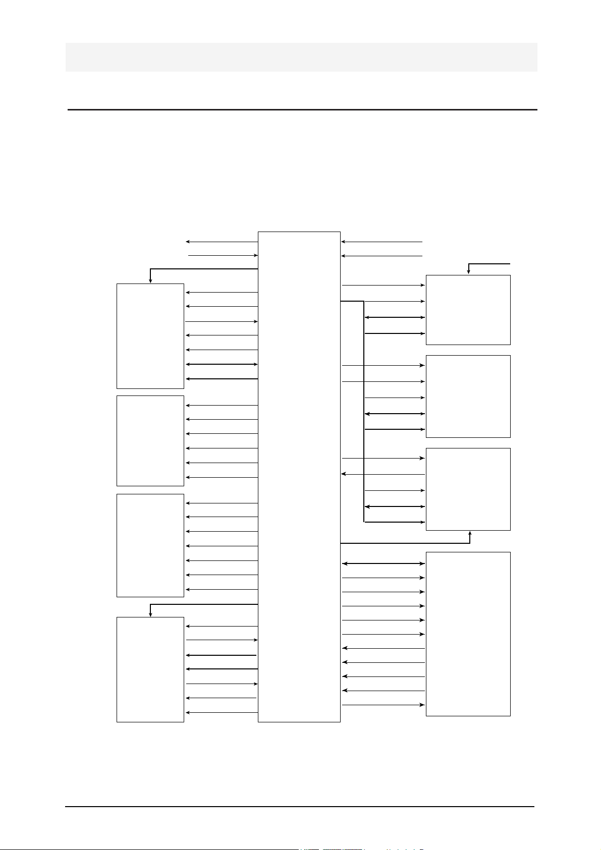
The main circuit that consists of CPU, MFP controller (built-in RISC processor core:
ARM7TDMI) including various I/O device drivers, system memory, scanner, printer,
motor driver, PC I/F, and FAX transceiver controls the whole system. The entire
structure of the main circuit is as follows:
Fig.5-1-1. Entire Structure of Main Circuit for Each Key Signal
LIU-TXD
MCLK(30MHz)
/POR
/ROMCS
/RD, /WR
D0~D15
D0~D15
D0~D7
A0~A17
A0~A9
A0~A4
/RST-OUT
PD0~PD7
/P-ERROR
/P-PE
/P-BUSY
/P-ACK
/P-SLCT
/P-INIT
/P-STB
245DIR
/P-SLCTIN
/P-AUTOFD
/MCS
/MIRQ
/RD, /WR
/RASO, 1
/WR
/UCAS,
/LCAS
/F-POR
LIU-RXD
IP-CLK
/XDACK
/XDREQ
/IP-CS
/RD, /WR
D0~D15
A0~A4
LFPHA
MFP CONTROLLER
(KS32C6200)
LFPHB
LFIA0
LFIA1
LFIB0
LFIB1
CR-REF
CRPHA
CRPHB
CRIA0
CRIA1
CRIB0
CRIB1
/HEAD-EN
HEAD-DATA
/HGA1~/HGA13
HOE1~HOE16
OK2PRINT
/FAULT-TEST
BIASOFF
/RST-OUT
/RST-OUT
LIU (STI9510)
COKOR IMAGE
PROCESSOR
FLASH
MEMORY
DRAM
MODEM
PARALLEL
INTERFACE
(IEEE1284)
LF MOTOR
DRIVER
CR MOTOR
DRIVER
PRINT HEAD’
DRIVER &
PRINT
CONTROL
CIRCUIT
Page 2

5-2 Samsung Electronics
MFP Controller consists of CPU(ARM7TDMI RISC processor), 2K-byte cache, data and address buses, serial
communication part with LIU(Line Interface Unit), print head controller, parallel port interface, external
DMA part to receive data from external color image processor (CIPIA:U17), LF/CR motor diver controller and
I/O controller.
5-1-2-1. SYSTEM CLOCK
The internal clock frequency is 30MHz. 30MHz system clock (MCLK) supplied from the outside is used without being divided inside.
5-1-2-2. DATA & ADDRESS BUS CONTROL
¥ /RD & /WR
/RD & /WR signals are synchronized with MCLK(30MHz) and become LOW ACTIVE.
These signals are strobe signals used to read and write data when each CHIP SELECT is connected with
/RD and /WR pin of RAM, ROM, MODEM and the outside devices and becomes active.
¥ CHIP SELECT (/CSO, /ROMCS, /MCS)
- /IP-CS : CIP1A(U17) CHIP SELECT (LOW ACTIVE)
- /ROMCS : ROM/FLASH MEMORY(U10) CHIP SELECT (LOW ACTIVE)
- /MCS : MODEM(U21) CHIP SELECT (LOW ACTIVE)
When each CHIP SELECT is low, data can be read or written.
¥ D0 - D15
- 16bit data bus
¥ A0 - A17
- ADDRESS BUS (A18 - A21 are reserved.)
5-1-2 MFP CONTRLLER (KS32C6200 : U15)
Page 3
Samsung Electronics 5-3
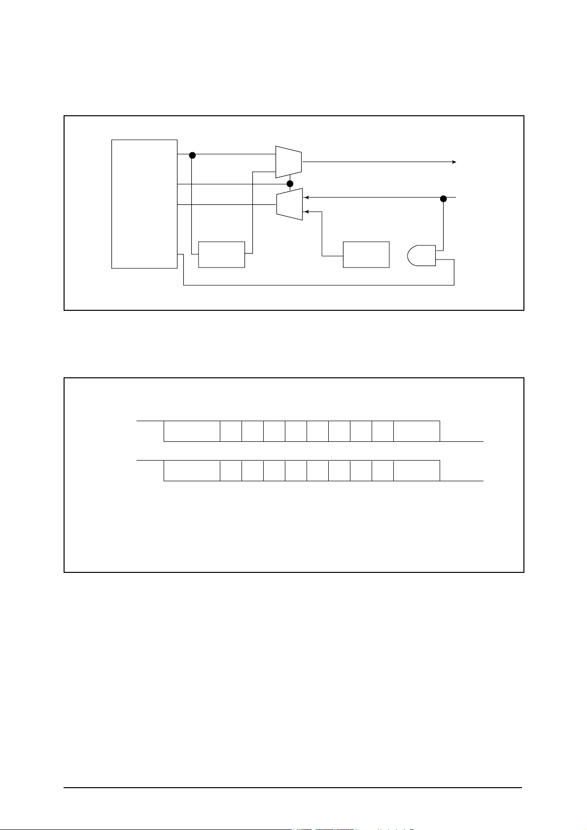
UART (Universal Asynchronous Receiver/Transmitter) at KS32C6200 enables the main and LIU to transmit
serial data. The block diagram of UART is as follows: (Fig.5-1-2) KS32C6200 has 2 UART channels. Channel
0(RXD0, TXD0) is used here and the baud rate is 9600bps.
5-1-2-3, LIU(Line Interface Unit) SERIAL COMMUNICATION PART
TxD
TxD
RxD
IRS
RE
IR Tx
Encoder
IR Rx
Decoder
0
0
1
1
RxD
UART
Block
Fig.5-1-2. UART BLOCK DIAGRAM
TXD :
START D0 D1 D2 D3 D4 D5 D6 D7 STOP
RXD :
START D0 D1 D2 D3 D4 D5 D6 D7 STOP
Fig.5-1-3 UART DATAFORMAT
START, STOP : 1BIT EACH
BAUD RATE : 9600bps
CPU I/F : SUPPORTS BOTH INTERRUPT & POLLING DRIVEN
PARITY : NO
Page 4
5-4 Samsung Electronics
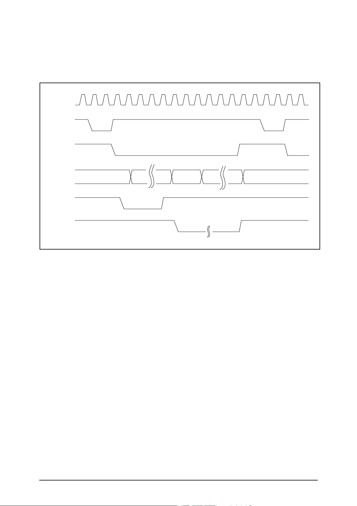
It brings data from an external device (CIP1A:U17) using DMA channel 0. DMA REQUEST sent from an
external device to KS32C6200 activates DMAACKNOWLEDGE signal and drives DMAchannel 0 to produce
CHIP SELECT and READ STROBE (/RD) at the external device and bring data from it. It generates address
of destination memory, CHIP SELECT and WRITE STROBE (/WR) in order to move this data into
destination memory, and then stores the data.
5-1-2-4 External DMA
MCLK
/XDREQ
/XDACK
D[15:0]
/RD
/WR
Fig.5-1-4 EXTERNAL DMA TIMING DIAGRAM
Page 5
Samsung Electronics 5-5
As KS32C6200 has DRAM controller in it, DRAM can be connected with external memory. The control mode
of DRAM controller enabling EARLY WRITE, NORMAL READ, PAGE MODE, and BYTE/HALF WORD
ACCESS supports EDO DRAM as well as normal DRAM. DRAM READ/WRITE signals are /RD and /WR
signals used to control system buses. It supports CAS BEFORE RAS for DRAM REFRESH and self-refresh
mode for DRAM backup. Connected with common /LCAS, /UCAS and RAS[1:0], it consists of 2 banks.
Though each may be connected with up to 1M - 4M halfword, 512 Kbytes or 2 Mbytes are connected according to the model for this product.
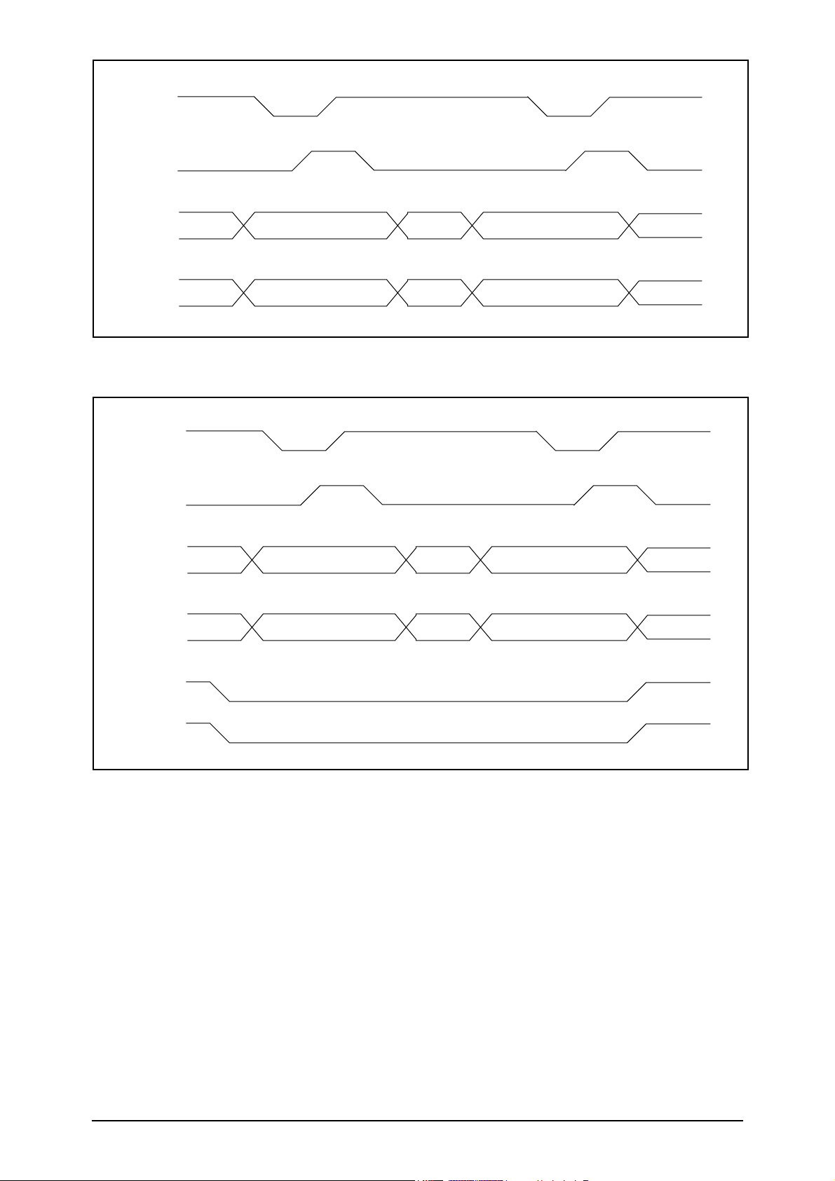
5-1-2-6. PARALLEL PORT INTERFACE
This part connected with the computer through the centronics connector makes possible parallel interface
with the computer. Data is transmitted according to the standard of IEEE P1284. This MFP controller supports
compatibility mode the traditional way to transmit print data, nibble mode (4bit data) to upload data to the
computer, and duplex high-speed transmission with the computer ECP(Extended Capabilities Port: 8bit data
transmission) all together.
It enables PC data to be printed and scanned data to be uploaded quickly to the computer. Besides, various
data transmission and reception with the computer such as uploading received fax data, downloading fax
data to be sent, and monitoring system control signals and system conditions are carried out here.
5-1-2-5. DRAM CONTROLLER
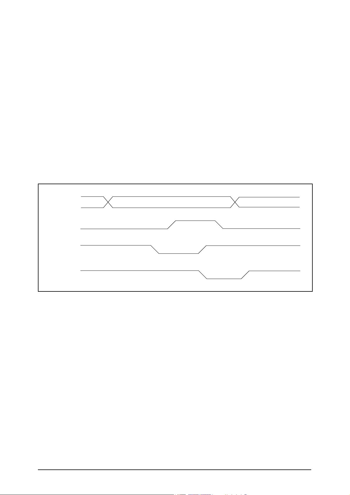
PPD(7 : 0)
DATA
BUSY
nSTROBE
nACK
Fig.5-1-5 Compatibility Hardware handshaking Timing
Page 6
5-6 Samsung Electronics
nSTROBE
BUSY
PPD(7 : 0)
nAUTOFD
BYTE0
DATA BYTE COMMAND BYTE
BYTE1
Fig.5-1-6 ECP Hardware Handshaking Timing (forward)
nACK
nAUTOFD
PPD(7 : 0)
BUSY
nINIT
PE
BYTE0
DATA BYTE COMMAND BYTE
BYTE1
Fig.5-1-7 ECP Hardware Handshaking Timing (reverse)
Page 7
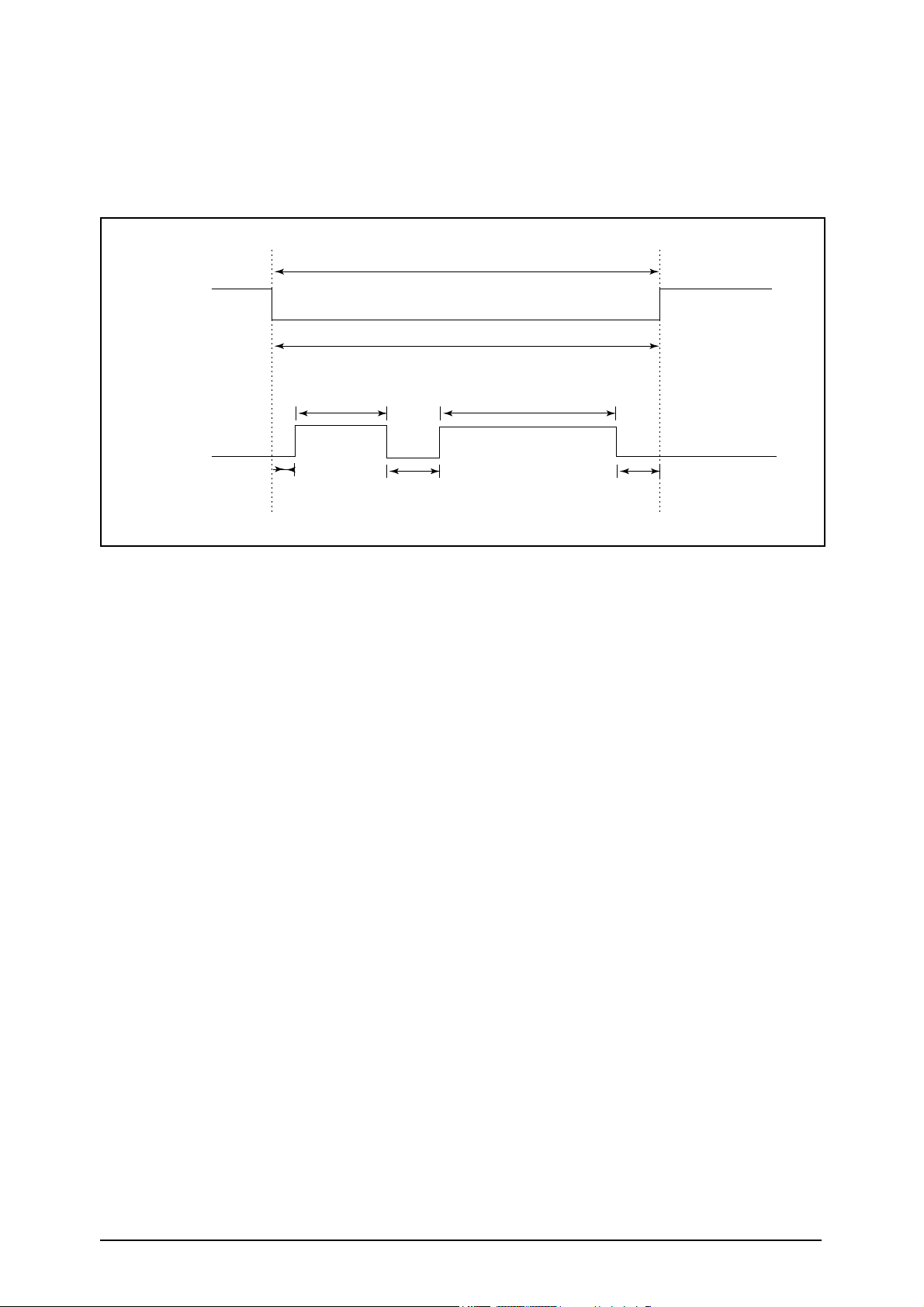
Samsung Electronics 5-7
This part produces major control signals used to drive INKJET head. It consists of signals to drive head nozzles, /PHGA[13:1], PHOE[16:1], /FAULT-TEST, /HEAD-EN, and BIASOFF, and consists of signals to check
the status of the head, OK 2PRINT and HEAD-DATA.
It has double height print head system, 208 nozzles for mono and 192 nozzles for color, and uses
/PHGA[13:1], /PHOE[16:1] signals and /HEAD-EN to drive these nozzles. Fig.5-1-8 is timing diagram of
each signal.
5-1-2-7. INKJET HEAD CONTROLLER
/PHGA
Signal
PHOE
Signal
Fire Enable Timer
Pre-Heat Pulse Width
Front End Delay Back End DelayPr-Heat Delay Width
Fire Pulse Width
t
p (PD)
Fig.5-1-8 Timing Diagram to Drive Head
Page 8
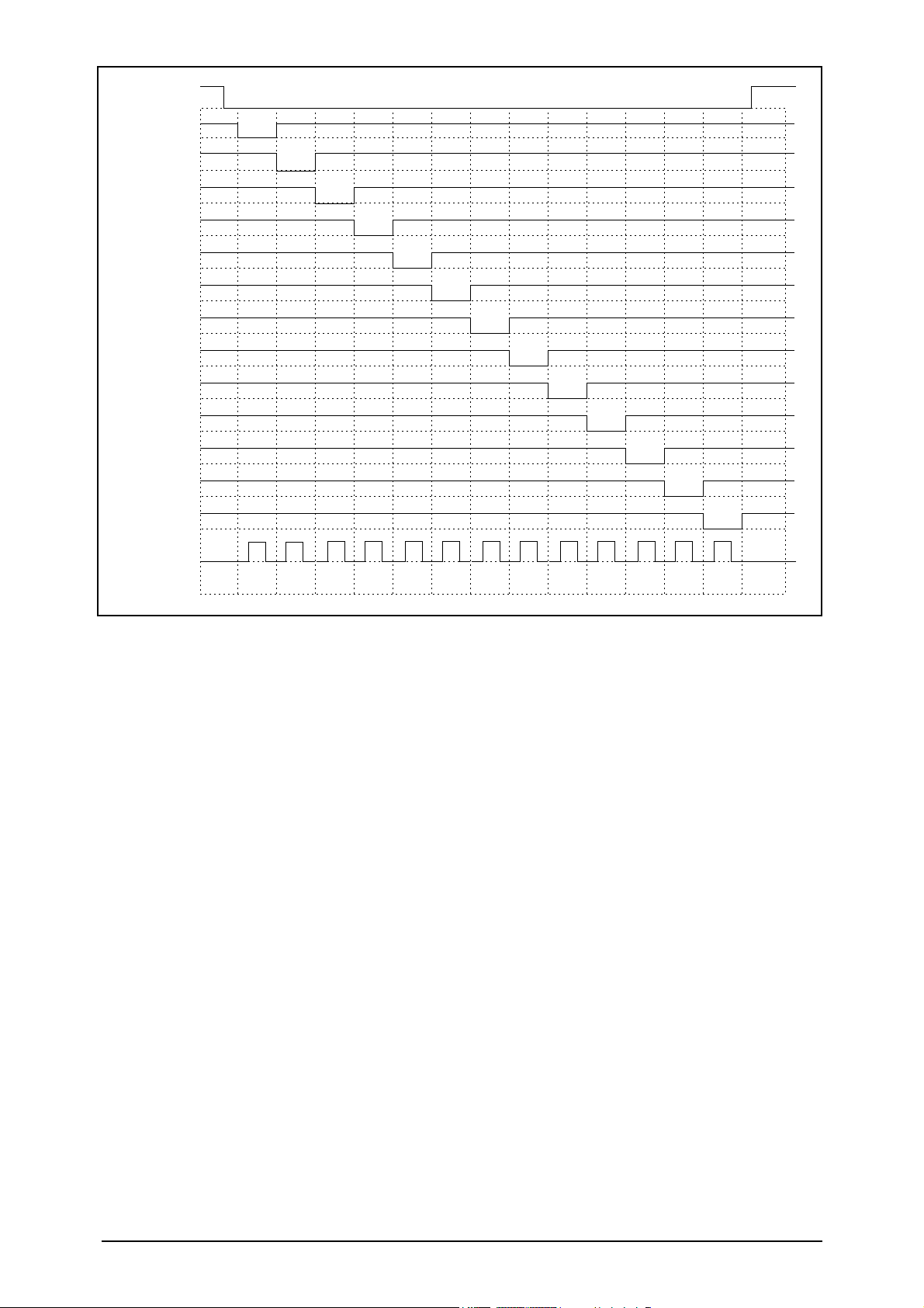
5-8 Samsung Electronics
/HEAD-EN
/PHGA1
/PHGA2
/PHGA3
/PHGA4
/PHGA5
/PHGA6
/PHGA7
/PHGA8
/PHGA9
/PHGA10
/PHGA11
/PHGA12
/PHGA13
(Tp)
PHOE1-
PHOE16
Fig.5-1-9. Timing Diagram for Each Nozzle
The above control signals are sent to head driver and the head driver converts these signals to the level
(+11.75V) to drive head nozzles.
5-1-2-8. MOTOR CONTROLLER (CRPHA, CRPHB, CRIA0, 1, CRIB0, 1, LFPHA, LFPHB, LFIA0, 1, LFIB0, 1)
MFP Controller (KS32C6200:U15) supports 2 stepper motors. It controls CR(Carriage Return) motor used to
read and print documents and LF (Line Feed) motor used to feed and eject paper.
CR motor controller can support 75, 150, 200, 300, 600, or 1200dpi according to resolution, while LF motor
controller supports uni-polar and bi-polar according to the kind of motors. Though full step, half step and software control are possible for both, bi-polar CR motor is controlled half step and LF motor is controlled half
step and quarter step here.
Page 9
Samsung Electronics 5-9
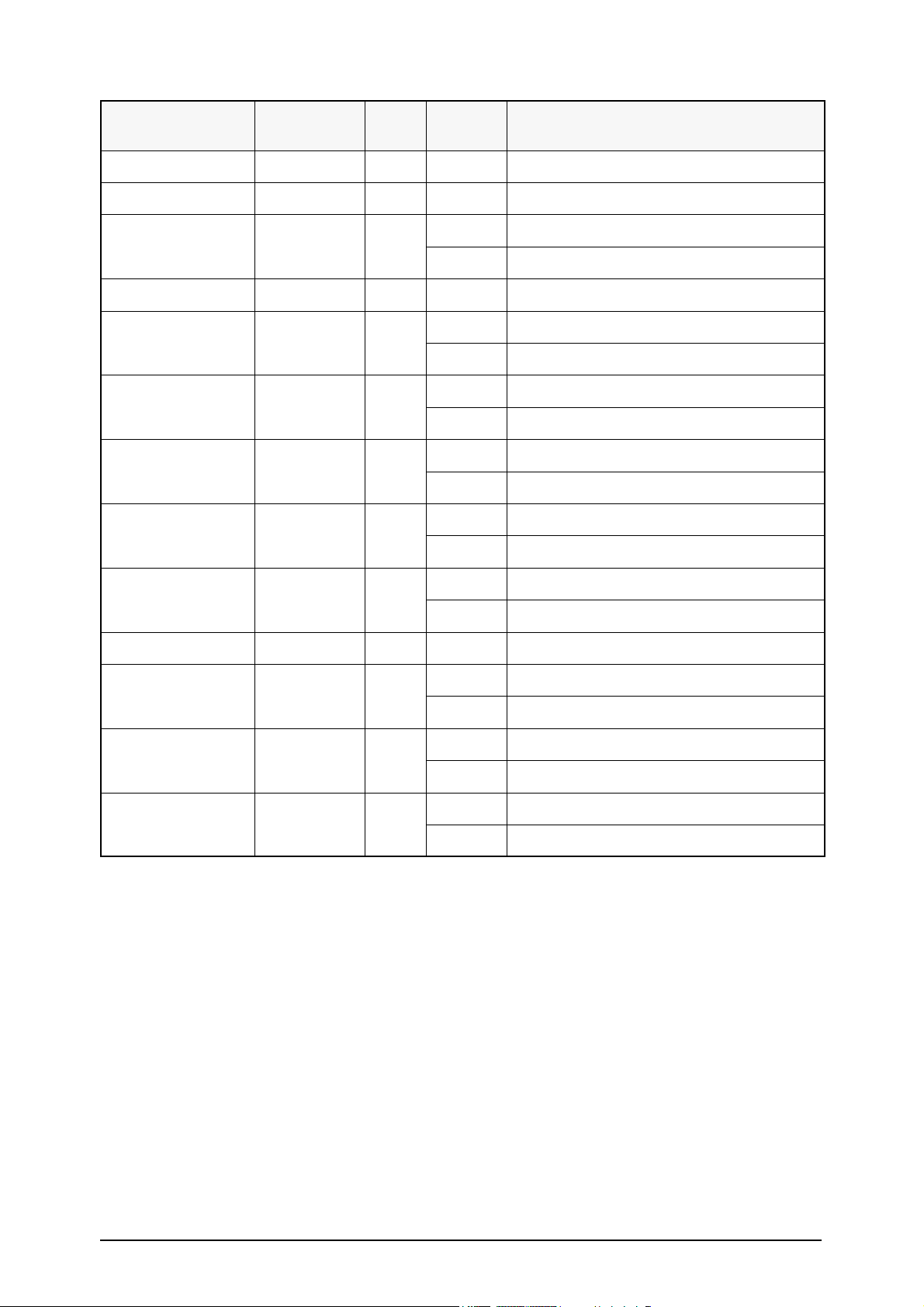
5-1-2-9. I/O PORT OF KS32C6200
PIN NAME
CIRCUIT NAME
I/O STATE DESCRIPTION
TXD 0 /GOP 0 LIU-TXD 0 - UART DATA TO I-LIU CHIP IN LIU
TXD 1 /GOP 1 - 0 - UNUSED
/EDACK /GOP 2 /XDACK 0
H DEFAULT STATE
L DMA ACKNOWLEDGE
TONE / GOP 3 KEYCLICK 0 - BEEP TONE
/RSTO / GOP 4 /RESET 0
H WATCHDOG RESET OUT IS INACTIVE
L WATCHDOG RESET OUT IS ACTIVE
/IOWR 1 / GOP 5 /FAULT-TEST 0
H DEFAULT STATE
L CHECK FAULT IN PRINTHEAD
/IOWR 2 / GOP 6 RX-CTL 0
H MODEM RX PATH CONNECTION
L
REMOTE START DETECTION PATH CONNECTION
/IORD 1 / GOP 7 /HEAD-EN 0
H PRINTHEAD IS DISABLE
L PRINTHEAD IS ENABLE
/IORD 2 / GOP 8 TONE-CTL 0
H MONITORING TX/RX SOUND
L BEEP SOUND
CLKOUT / GOP 9 IP-CLK 0 - CIP CLOCK
FIREPS / GOP 10 /RST-OUT 0
H EXT. CHIP IS ACTIVE
L EXT. CHIP IS RESET
/HSC / GOP 11 BIASOFF 0
H PRINTHEAD BIAS OFF
L PRINTHEAD BIAS ON
/HSM / GOP 12 CR-REF 0
H PRINT MODE IS LQ
L PRINT MODE IS DRAFT
Page 10
5-10 Samsung Electronics
PIN NAME
CIRCUIT NAME
I/O STATE DESCRIPTION
RXD 0 / GIP 0 LIU-RXD I - UART DATA FROM I-LIU CHIP IN LIU
RXD 1 / GIP 1 /P-EXIT I
H PAPER IS NOT DETECTED
L PAPER IS DETECTED
/EINT 1 / GIP 2 /MIRQ I
H NO INTERRUPT FROM MODEM
L INTERRUPT FROM MODEM
/EINT 2 / GIP 3 OK2PRINT I
H NO FAULT IN PRINTHEAD
L FAULT IN PRINTHEAD
/EDREQ / GIP 4 /XDREQ I
H NO DMA REQUEST FROM CIP
L DMA REQUEST FROM CIP
UCLK / GIP 5 HEAD-DATA I - CODE DATA FROM PRINTHEAD
TCK / GIOP 0 TCK I/O - TEST PIN FOR EMULATOR (CLOCK)
TMS / GIOP 1 TMS I/O - TEST PIN FOR EMULATOR (DATA MODE)
TDI / GIOP 2 TDI I/O -
TEST PIN FOR EMULATOR (DATA FROM EMULATOR)
/TRST / GIOP 3 /TRST I/O -
TEST PIN FOR EMULATOR (RESET TO TAP CON.)
TDO / GIOP 4 TDO I/O -
TEST PIN FOR EMULATOR (DATA TO EMULATOR)
Page 11
Samsung Electronics 5-11
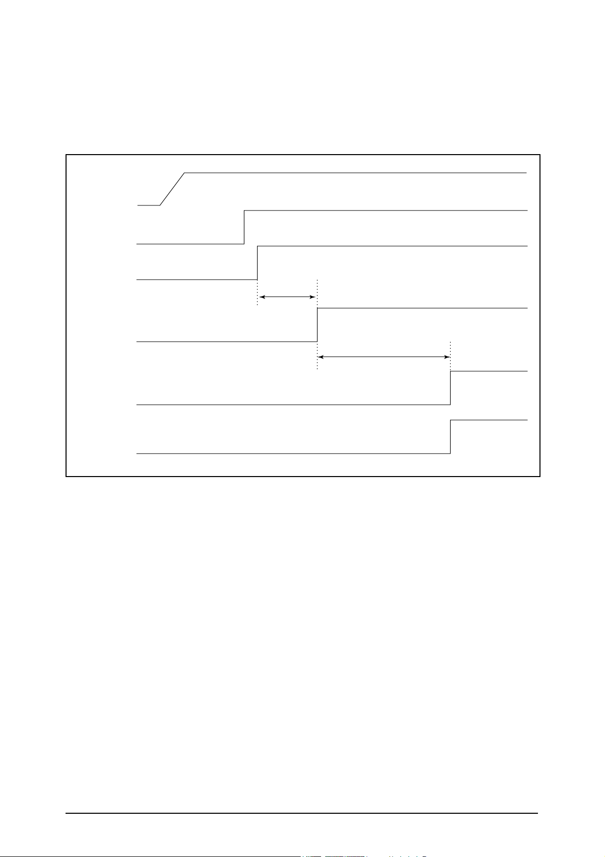
As for SMARTJET there are 2 power resets of primary reset(/F-POR) and secondary reset(/POR) and also
reset by watchdog timer (/RSTO). Primary reset is used to initialize flash memory when the system is turned
on, while secondary reset is used to initialize the whole system by initializing MFP controller (KS32C6200)
after primary reset. Primary reset makes flash memory wait in READ mode to fetch program codes, and secondary reset makes the main controller (KS53C6200) wake up and initialize external peripherals to operate
the system. Fig.5-1-10 is Power Reset Timing Diagram.
5-1-2-10. RESET CIRCUIT
supply
Voltage
/F-POR
/POR
PnRST
Internal Reset
256 MCLK
Reset filter
65 MCLK
ROM Access
(internal)
Reset
Fig.5-1-10 POWER RESET TIMING DIAGRAM
Page 12

5-12 Samsung Electronics
¥ POWER MONITOR (U16: KIA7045F)
If +5V supplied to KIA7045F is so unstable as to reach +4.65V - +4.35V (typically 4.5V), it will recognize it
as power failure. Then KIA7045F output terminal becomes low (0V) and the voltage is impressed to flash
memory and KS32C6200, running RESET (LOW ACTIVE). Flash memory and KS32C6200 are reset first.
Thereafter modem, print control parts and CIP(Color Image Processor) linked to /RST-OUT terminal of
KS32C6200 are reset as well. KIA7045F output terminal of open drain structure is pulled up 5.1k½ and put
out.
5-1-3 SYSTEM MEMORY
System memory consists of 512KB flash memory and 2MB DRAM. Flash memory and DRAM are selected by
each CHIP SELECT (/ROMCS, /RASO, /RAS1, /LCAS, /UCAS), and data is accessed half word (16bits) by
half word.
Page 13

Samsung Electronics 5-13
5-1-4 SCANNER
5-1-4-1. SUMMARY
This product has CCD(Charge Coupled Device) as an image sensor to receive image input signals and has
embodied a shuttle scanner, realizing various scanner control signals and image processing with color image
processor CIP1A(U17), which is ASIC for shuttle scan. We are going to look into the principles by explaining
the whole data flow in the scanner, block diagram of CIP1A, allocated I/O port and peripheral circuits.
5-1-4-2. CIP1A(U17)
The inside of ASIC is roughly divided into A/D Converter to convert image signals to digital signals, Scanner
Controller to provide various CCD driving signals and signals to interface with host controller, and Image
Processor for shading compensation, gamma compensation and reasoning of image signals.
CCD
Module
CIP-1A
A/D
Converter
Scanner
Controller
MFP
Controller
Image
Processor
Data
Memory
Analog
Data
CCD
Control
Pixel
Data
Digitized
Data
DMA
Control
System
Data BUS
Data
Timing
IP
Control
CIP-I Control Data
+
Formatted Data for DMA
Formatted Data for DMA
CIP-I Control Data
Processed
Data
A/D
Sample
Clock
fig.5-1-11 CIP1ABlock Diagram
Page 14

5-14 Samsung Electronics
PIN PIN
I/O
CIRCUIT DESCRIPTION
NAME NO. NAME
HL
GIP 0 12 I /START-KEY -
FAX START / COPY KEY
PRESSED
GIP 1 13 I /CART-KEY -
CARTRIDGE CHANGE KEY
PRESSED
GIP 2 14 I /POW-KEY -
POWER(READY) KEY
PRESSED
GIP 3 15 I /STOP-KEY -
FORM FEED / STOP KEY
PRESSED
GIP 4 17 I THMST CCD LAMP OVER HEAT CCD LAMP NORMAL
GIP 5 18 I /RINGDET -
RING DETECTION FROM
TEL LINE
GIP 6 19 I /HOOK-OFF EXTERNAL PHONE HOOK ON
EXTERNAL PHONE HOOK OFF
GIP 7 20 I HOME-SEN PRINT HEAD PARKING PRINT HEAD MOVING
GOP 0 2 O SHAD-ON SHADING ENABLE -
GOP 1 3 O /SHAD-RST
SHADING REFERENCE CLEAR
-
GOP 2 4 O POW-LED POWER (READY) LED ON POWER(READY) LED OFF
GOP 3 5 O BUSY-LED BUSY LED ON BUSY LED OFF
GOP 4 7 O SCAN-LED FAX LED ON FAX LED OFF
GOP 5 8 O CML-CTL
FAX OR TEL LINE CONNECTED
EXT. PHONE CONNECTED
GOP 6 9 O LAMP-5V CCD MODULE RETURN (+5V) -
GOP 7 10 O LAMP-12V CCD LAMP ON (+11.75V) -
5-1-4-3 CIP1A I/O Port
Page 15

Samsung Electronics 5-15
PIN PIN
I/O
CIRCUIT DESCRIPTION
NAME NO. NAME
HL
GIOP 0 21 O THM-CLK CLOCK SIGNAL TO DIGITAL THERMISTER : 100~140kHz
GIOP 1 22 I/O THM-DATA DATA FROM/TO DIGITAL THERMISTER
GIOP 2 23 O PRE-HEAT PRINT HEAD PREHEATING -
GIOP 3 24 I P-EMPTY NO PAPER PAPER READY
GIOP 4 25 O /SPK-CTL AUDIO AMP. OFF AUDIO AMP. ON
GIOP 5 26 O FAX-LED FAX LED ON FAX LED OFF
GIOP 6 27 I FM-STAT
FLASH MEMORY STATUS FLASH MEMORY STA
TUS
READY BUSY
GIOP 7 28 O CLK-SEL MCLK/2 MCLK
5-1-4-4. PERIPHERAL CIRCUIT
As to the power of lamp, light source of the scanner module, +11.75V(while scanning) supply and +5V(while
waiting) supply are switched by transistor Q7,8,9, and 11.
-Vref is supplied with 1.5V by resistance division through OP-Amp, while +Vref detects the peak by control
of analog Mux U2 during white reference label shading. It detects the peak level of image signals by dividing
shad-on signal and /Shad-rst signal of U2 into High, setting it as top standard voltage. When you scan some
image actually, it will drive shad-on signals into Low to keep the peak level of the capacitor. When you finish
scanning, it will drive /Shad-rst into Low and discharge electricity.
Image signals from CCD mounted on scan PBA in the shuttle scanner are delivered through FPC cable, shifting the level as much as 0.75V at Emitter terminal of Tr which is turned on by Level SH signal. These image
signals will double by an non-inverting amplifier and finally 1.5V level-shifted image signals will be put in
CIP1A.
Page 16

5-16 Samsung Electronics
5-1-5 PRINTER
5-1-5-1. GENERAL
It drives inkjet head to print printing data received from the computer or fax data coming through the line. It
roughly consists of head driver, head controller, and the ambient temperature sensor. Fig.6-1-11. Block
Diagram of Printer shows the entire structure.
5-1-5-2. HEAD DRIVER (U19, U20, U23, U24)
This part drives and inks inkjet head. Color inkjet head drives 192 nozzles, while mono inkjet head drives 208
nozzles. Mono inkjet head is composed of 16 groups of 13 nozzles. As to the driver that composes each nozzle, 13 row 7-bit driver (U23, U24) selects head address and 16 column 8-bit driver (U19, U20) sends head data.
Head driver converts control signals from MFP controller to +11.75V, the level to be able to drive the head,
and provides them for the inkjet head.
¥ Row Driver Circuit (HD7:U23:U24)
This is a 13-line signal impressed to row drive IC through the output port of MFP controller(/PHGA1 - /PHGA13),
used as an address to drive the head in ink cartridge. Pulse period differs according to head driving frequency. In
1200dpi (in case of Head: 12KHz) mode, timing period is 2.6usec (1/1200Ö16 groups). The signal put in each driver(window time) is active ÒLÓ, with the biggest driver current max 100mA and output voltage +11.75V.
¥ Column Driver Circuit (HD8:U19,U20)
It is the fire enable pulse of real head. 16 lines are put out as head driving data lines through the output port of MFP
controller (PHOE1 - PHOE16). Enable pulse impressed to the head is put out within window time (Low). It has the
function to move it forward or backward by the register in MFP controller. Besides the output signal may differ in
accordance with the type of head (mono or color). If there is data, printing image is put out at ÒHÓ. If not, it is put
out at ÒLÓ. In case of Babbage head, pulse width is always 1.3use regardless of the type of the head, with the maximum driving current 400mA and output voltage +11.75V.
Page 17

Samsung Electronics 5-17
5-1-5-3. HEAD CONTROLLER
This part consists of +22V Power Controller to control head driver, Fault Test, Head Detection, Substrate
Heating and ambient Temperature Sensor. It checks and controls head driver and ink cartridge.
KS32C6200
(U15)
Ink
Cartridge
(Mono)
or
(Color)
MFP
CONTROLLER
CIP 1A(U17)
IMAGE
PROCESSOR
/FAULT-TEST
/HGA1
/HGA13
HOE1
HOE16
/FAULT-TEST
OK2PRINT
BIASOFF
HEAD-DATA
/HEAD-EN
PRE-HEAT
BH1,BH2
HSM
BS1
THM-DATA
THM-CLK
BP1
BA13
BA1
BP16
/FAULT
HEAD-DATA
Fig.5-1-12 Block Diagram of Printer
Page 18

5-18 Samsung Electronics
¥ +22V Power Controller
If you insert power cords, the main board will be supplied with power. /POR signal put out through reset
circuit activates MFP controller (K32C6200:U15) and MFP controller puts out external circuit reset signal
/RST-OUT. This /RST-OUT signal and Vrefx (+2.5V) divided through +30V are impressed to the input terminal of the comparator, putting out +22V if the output of the comparator is ÒhighÓ or getting turned off if
ÒlowÓ.(in case of /FAULT-TEST signal: HIGH) While +22V is being impressed after /RST-OUT is ÒHighÓ,
comparator output gets ÒlowÓ and turns off +22V driving TR(TIP112) if /FAULT-TEST signal is put out at
ÒlowÓ when you check a short of the head driver and the ink cartridge (head).
¥ FAULT TEST CIRCUIT
This is a signal to detect whether the head receiving the output of head column driver is in a short. After
/FAULT-TEST signal is put out at ÒlowÓ and +22V is turned ÒoffÓ, ÒOK2PRINTÓ signal is entered. The port
of KS32C6200(U15) shows normal condition if ÒHÓ and a short if ÒLÓ. If you make FAULT-TEST output ÒLÓ
to detect fault of the head, +22V gets off. If the head is in a short (LOW), when the level of Ò/FAULT-TESTÓ
signal goes ÒLÓ and final ÒOK2PRINTÓ output goes ÒLÓ. KS32C6200(U15) reads this signal and checks
whether the head input receiving the driver output is in a short. Diode cathode is attached to each output
transistor collector in the column driver. 8 anode terminals of diode become common as one and put out
/FAULT signal, which is pulled up by bias circuit controlled by /FAULT-TEST and shows the condition by
OK2PRINT through the comparator.
¥ SUBSTRATE HEAT CIRCUIT
Mono ink cartridge of Babbage head is 600dpi head that uses pigment ink. It is very sensitive to the temperature in and around the cartridge. In particular, the viscosity of ink affects print quality as it is inversely
proportional to temperature by an exponential function. This signal used to compensate it helps you get
equal inking quality by warming the ink chamber in the cartridge with aluminum pattern heater before
starting to print if the surrounding temperature is lower than standard (below 35¡É).(Refer to Timing
Chart.) It sends PRE-HEAT signal through I/O port of CIP1A(Color Image Processor:U17) and supplies
+11.75V.
Mono Head
Fig.5-1-13. Temperature around Mono Head
Pre-Heat if below 35¡c
70°C
35°C
Page 19

Samsung Electronics 5-19
Color Head
Fig.5-1-14. Temperature around Color Head
Fig.5-1-15. HEAD DETECTION TIMING DIAGRAM
No Pre-Heating
¥ HEAD DETECTION CIRCUIT
Babbage ink cartridge has 8-bit mask ROM I.D. to check the type of cartridge. In order to detect the head,
HSM signal is used as ENABLE signal and BA3 signal as START & STOP BIT, and BA1 and BA2 as clock
signal of each bit, and ID signal in the cartridge is put in HEAD-DATA port of KS32C6200 through BS1 line.
With each bit controlled, 8bit I.D data is read and STOP bit is put out of BA3(LOAD) port. Then it finishes.
If data is mono, it is 07H. If color, 08H.
70°C
t
HSM
(Pwr)
BA3
(Load)
BA1
(Clock1)
BA2
(Clock2)
HEAD-DATA
bit7
Head I.D read : HEAD-DATA
Mono : 07H
Color : 08H
Min 500ns Clock Delay
bit6 bit5 bit4 bit3 bit2 bit1 bit0
Page 20

5-20 Samsung Electronics
¥ SURROUNDING TEMPERATURE SENSOR
DS1621S(DALLAS SEMI.) is applied to read the temperature around ink cartridge. It is used to get optimum
inking quality by keeping the viscosity of ink in the cartridge in the specified lerel. The way to read temperature is similar to EEPROM, controlled by THM-CLK, THM-DATA LINE. Digital thermometer to check
the surrounding temperature is assembled along with home sensor in the frame of assembly CR. After each
line is printed, it reads the surrounding temperature and heats substrate heater in the ink cartridge during
the accelerating time of CR to keep the viscosity of ink in the specified lerel.
5-1-5-4. HEAD DRIVING TIMING
Control signal from MFP controller (KS32C6200:U15) enters the head driver and it becomes the level to be able
to drive the head nozzles (+11.75V). It is depicted in the following diagram.
BA
Signal
t
p(PD)
BP
Signal
Pre-Heat Pulse Width Fire Pulse Width
Fire Enable Timer
Pre-Heat Delay Width
Front End Delay
Back End Delay
Fig.5-1-16. HEAD DRIVING TIMING DIAGRAM
Page 21

Samsung Electronics 5-21
HSM
BA1
BA2
BA3
BA4
BA5
BA6
BA7
BA8
BA9
BA10
BA11
BA12
BA13
(Tp)
BP1-
BP16
Fig.5-1-17. TIMING DIAGRAM FOR EACH NOZZLE
Page 22

5-22 Samsung Electronics
5-1-5-5. INK CARTRIDGE
¥ PIN ARRAY OF MONO INK CARTRIDGE
There are 208 heater chips in mono ink cartridge.
Column
Address (BA1_ ~ BA13_)
Data(BPx)
12345678910111213
1 1 21 15 9 3 23 17 11 5 25 19 13 7
2 20 14 8 2 22 16 10 4 24 18 12 6 26
3 2747413529 494337 3152 453933
4 4640342849 423630 5044 383252
5 5373676155 756963 5777 716559
6 7266605474 686256 7670 645878
7 79 99 93 87 81 101 95 89 83 103 97 91 85
8 98 92 86 80 100 94 88 82 102 96 90 84 104
9 105 125 119 113 107 127 121 115 109 129 123 117 111
10 124 118 112 106 126 120 114 108 128 122 116 110 130
11 131 151 145 139 133 153 147 141 135 155 149 143 137
12 150 144 138 132 152 146 140 134 154 148 142 136 156
13 157 177 171 165 159 179 173 167 161 181 175 169 163
14 176 170 164 158 178 172 166 160 180 174 168 162 182
15 183 203 197 191 185 205 199 193 187 207 201 195 189
16 202 196 190 184 204 198 192 186 206 200 194 188 208
Page 23

Samsung Electronics 5-23
¥ PIN ARRAY OF COLOR INK CARTRIDGE
There are 192 heater chips in mono ink cartridge. One cartridge has 64 Cyan, 64 Magenta, 64 Yellow heaters
and (64 x 3 colors) 192 nozzles.
Column
Address (BA1_ ~ BA13_)
Data(BPx)
12345678910111213
1 - 19 13 7 11 21 15 9 3 23 17 11 5
215126-201482221610424
3 2545393327 474135 2949 433731
4 4438322646 403428 4842 363050
5 5171655953 736761 5575 696357
6 7064585272 666054 7468 625676
7 77 97 91 85 79 99 93 87 81 101 95 89 83
8 96 90 84 78 98 92 86 80 100 94 88 82 102
9 103 123 117 111 105 125 119 113 107 127 121 115 109
10 122 166 110 104 124 118 112 106 126 120 114 108 128
11 129 149 143 137 131 151 145 139 133 153 147 141 135
12 148 142 136 130 150 144 138 132 152 146 140 134 154
13 155 175 169 163 157 177 171 165 159 179 173 167 161
14 174 168 162 156 176 170 164 158 178 172 166 160 180
15 181 - - 189 183 - - 191 185 - - - 187
16 - - 188 182 - - 190 184 - - 192 186 -
Page 24

5-24 Samsung Electronics
5-1-6 MOTOR DRIVER
5-1-6-1. GENERAL
SMARTJET use 2 stepper motors, i.e. CR(Cartridge Return) motor and LF(Line Feed) motor.
CR motor moves left and right all-in-one carriage of inkjet head and shuttle scanner. It helps the printer print
accurately on the paper and the scanner read image data accurately. LF motor is driven to feed and eject
paper for printing and to feed and eject documents to read for scanning. Bi-polar CR motor is controlled half
step with maximum 24ips(inch/sec), while LF motor half step and quarter step at maximum 6ips.
5-1-6-2. CR(CARRIAGE RETURN) MOTOR DRIVING CIRCUIT
CR motor moves the carriage left and right when ink cartridge prints something on paper or shuttle scanner
reads image data.
- Motor Type : Stepper motor, bi-polar
- Driving Voltage : +30V
- Winding Resistance : 6½ ± 10%
- Driving IC : TEA3718DP X 2
CR_REF
CRIA1 CRIA0
CURRENT(mA) OPERATION REMARK
(CRIB1) (CRIB0)
H L L 490 Mono LQ is being driven
L L L 670 Color draft is being driven
L L L 670 Mono draft is being driven
X H H 0 No current
As shown in the above table, current in each mode is adjusted by voltage of driver(U25, U26) CRVREF input.
If the output of CR_REF signal controlled by MFP controller(U15) is ÒlowÓ, TR(Q12) will be turned off and the
voltage put in to CRVREF of driver (U25, U26) with +5V divided will go up (+4.5V). It becomes the standard
of the driver, resulting in high current. If CR_REF output is ÒhighÓ, TR(Q12) will be turned on and the voltage put in to CRVREF will go down (+3.0V), resulting in low current in the motor.
Page 25

Samsung Electronics 5-25
5-1-6-3. LF(Line Feed) Motor Driving Circuit
LF motor is driven to feed and eject documents and paper.
- Motor Type: stepper motor, bi-polar
- Driving Voltage : +30V
- Winding Resistance : 12½ ± 10%
- Driving IC : PBL3717A X 2
LFIA1 LFIA0 CURRENT(mA) OPERATION REMARK
L L 670 When feeding document/paper
L H 400 When ejecting document/paper
X H 0 No current
Page 26

5-26 Samsung Electronics
5-1-7 FAX TRANSCEIVER
5-1-7-1. GENERAL
This circuit processes transmission signals of modem and between LIU and modem.
This circuit is added only to SMARTJET.
5-1-7-2. MODEM (U21)
KS16116 is a single chip fax modem. It has functions of DTMF detection and DTMF signal production as well
as functions of modem. TX OUT is transmission output port and RX IN is received data input port. /POR
signal controlled by MFP controller (U15:KS32C6200) can initialize modem(/RST_OUT) without turning off
the system.
D0 - D7 are 8-bit data buses. RS0 - RS4 signals to select the register in modem decide the mode. /CS is a signal to select modem chips. /RD and /WR signals control READ and WRITE respectively. /IRQ is a signal for
modem interrupt.
Transmission speed of KS16116 is up to 9600bps.
5-1-7-3. TRANSMITTER
This circuit processes transmission output, analog signal of modem(KS16116).
Output signal in each mode goes out of modem (TXOUT:U21-44). After D/A signals are smoothed and filtered through active filter (U5-6,7:R270,R277,C130), they are buffered under OP AMP(U5-2, 1:R291, C139,
R298, C150) and put out to LINE through LIU board.
5-1-7-4. RECEIVER
In the receiving mode, analog signals coming in through LIU board are amplified at OP AMP(U6-2, R293,
C141), and then transmitted to input terminal of modem (RXIN:U21-45) through smoothing filter (U6-6,
7:R273, R274, C126).
Fig.5-1-18. FAX TRANSCEIVER
FAX TRANSMISSION
FAX RECEPTION
MODEM
KS16116
(U21)
LIU
Page 27

Samsung Electronics 5-27
5-1-8 OTHERS
OPERATOR PANEL DESCRIPTION
KEY & LED DESCRIPTION
- When power cord is inserted, the system is turned on and initialized. It does not operate but
waits for Ready key to be pressed.
- If you press the Ready key, the nearby Ready LED will be turned on and the device will be
initialized with the system in standby mode.
- If the Ready LED is off, the system does not operate though it is on.
- Running Print Out Test Pattern
Step 1. While Ready LED is off, press ÔReadyÕ key for 0.5 - 1 second with ÔFF/Stop key pressed
in advance.
Step 2. Pattern is printed so that you can check the nozzles of the head.
- This key is used to exchange print head cartridge in the toggle mode or to insert it for the first
time.
- If color head is mounted when fax documents are to be printed,it does not print but Ready
LED and operating LED blink.
- Press this key for about 3 sec or more to put in a new ink cartridge.
- When Ôno paperÕ is displayed while printing, place paper, and it is automatically fed.
- After you finish printing, press this key to eject paper already fed.
- Press this key to stop fax communication.
- Press this key to stop scanning.
- If you press this key when hook-on and documents will be fed, scanned and stored in
memory.
- If you press this key when hook-on but there is no document, LED meaning ÔFeed documentÕ
will blink for about 3 sec. (Refer to LED status.)
- If you press this key when hook-off, it will operate to receive or transmit the document you
fed.
LED status
System Standby Mode. You can start new operation only in this mode. (TEL mode)
System Standby Mode. You can start new operation only in this mode. (FAX mode)
Data is being received from host.(Printing) other operation
Data is being uploaded to host. (Scanning) Fax transmitting/reception. (Faxing)
Transmitting/receiving error
Paper jam, no paper
No document, next document, document jam
Cartridge is being exchanged. No cartridge
Ink low
● ➞ green LED ON ➞ OFF ➞ green LED blinks
■ ➞ red LED ON ➞ red LED blinks
Ready Busy Scan/Fax
●
●
●
●
●
●
●
●
●
●
●
●
■
■
Ready Cartridge FF/Stop Start/Copy
Busy Scan/Fax
Ready
Cartridge
FF/Stop
Start/ Copy
Page 28

5-28 Samsung Electronics
5-2-1 SUMMARY
LIU(Line Interface Unit) circuit added only to SMARTJET is controlled by the main circuit.
It monitors telephone line and helps interface between the system and the telephone line. It uses 1LIU(STI9510) to control the whole LIU, MODEM/LINE INTERFACE, RING SIGNAL DETECTOR, DIALER,
LINE CURRENT DETECTOR, and SERIAL INTERFACE.
5-2-2 MODEM/LINE INTERFACE
This is the path through which transmitted and received data of modem is put in and out.
¥ CML1 Relay: It divides telephone line into external telephone and fax.
¥ U3-3 TIT(Transformer Input from Transformer): This single ended input receives image signals from
modem through transformer T2 and transmits them on telephone line.
¥ U3-40 ROT(Receive Output Transformer): This output transformer receives signals on telephone line and
delivers them to modem through transformer T1. It has AC impedance of 10Kohm or over.
¥ AC impedance: Normal operation range of U3(STI9510) is from 15mA to 100mA. DC characteristics depend
on the voltage of U3-37 LI(Line Input) terminal and the voltage of resistance R48 between U3-37 LI(Line
Input) terminal and U3-39 LS terminal.
5-2-3 RING SIGNAL DETECTOR
¥ U3-28(MO) terminals are ring signal output terminals. Q4 and Q5 put out ring signals and drive Piezzo, but
SmartJet2000, SMARTJET does not use Piezzo. It has only the functions related to ring detection such as driving the photocoupler of U4 and delivering ring signals to MFP controller (U15:KS32C6200) of the main.
5-2-4 DIALER
5-2-4-1. MF DIAL
¥ Default mode it is set in DP. You can change it to MF mode by control of MFP controller.
¥ MF signal can be measured at (tone level of low group: typical - 14dBm) U3-4 MFO(DTMF Generator
Output). The signal is adjustable by R40, R41 and C29. The adjusted signal enters U3-9 MFI (DTMF
Amplifier Input) and is amplified to be transmitted on telephone line.
¥ U3-39 LS(Line Current Sense Input) terminals show the final signals transmitted to telephone line.
5-2-4-2. DP DIAL
¥ If U3-2(DMS) is made Vcc by R42, it is set at 33:67 DP signal. If it is made Vss by R43, it is set at DP signal.
This product is set at DP signal.
¥ DP signal is made by U3-27(DPn) terminals. This signal turns on/off Q1. The signal made at that time turns
on/off Q2, which interrupts DC current on telephone line and puts out pulse signal on telephone line.
¥ U3-35 CS terminals : It makes Make Resistance by shorting telephone line with Vss during Make period of
DP dial.
5-2 LIU PBA
Page 29

Samsung Electronics 5-29
5-2-5 Line Current Detector
¥ When CML1 relay connects telephone line, U3(STI9510) of LIU board and MFP controller of the main board
(U15:KS32C6200) start communication through UART. U3 of LIU board sends signal that includes information of line current value, whenever it receives orders or data from U15 of the main board.
5-2-6 Serial Interface
¥ This part does serial communication with MFP controller of the main board (MAIN PBA:U15) that controls
the whole system. It controls LIU by giving and taking all control orders and line status.
¥ U3-11 RXD : Schmitt Trigger input, Receiving terminal..
¥ U3-29 TXD : Open Drain output terminal
¥ Standard UART communication
- Baud Rate : 9600bps
- Start, Stop bit : 1bit each
- Data bits : 8 bit
- Parity bit : none
5-2-7 MAJOR FUNCTIONS OF PARTS
1) U3 : STI9510
- Key part of LIU board. Speech Network, Dialer, Ringer and UART are built in one IC package.
2) U5 : PC817
- Photo coupler. It enables UART of U3(STI9510) to receive control signal or dialing information from
MFP controller of the main board (U15).
- Insulation between prinary and secondany circuit part.
3) U6 : PC817
- Photo coupler. It enables UART(U3-29:TXD) of U3(STI9510) to deliver telephone line status or
response signal about control signal or dialing information from LIU to MFP controller of the main
board (U15).
- Insulation between prinary and secondany circuit part.
4) U4 : PC817
- It senses and delivers ring signal to the main board.
- Insulation between prinary and secondany circuit part.
5) U2 : PC814
- It senses hook-off (Line connection) of the external telephone and delivers it to the main board.
- Insulation between prinary and secondany circuit part.
6) BD1 : BRIDGE DIODE
- Regardless of the polarity of DC power from telephone line, the voltage put out on Pin.1 has always
+ polarity against pin Pin.2. So DC loop forms always in the same direction regardless of the polarity of the telephone line.
7) T2,T3 : TRANSFORMER
- It delivers signals from the telephone line to modem or signals from modem to the telephone
line.
- Insulation between prinary and secondany circuit part.
Page 30

5-30 Samsung Electronics
5-3-1 BLOCK DIAGRAM OF POWER CIRCUIT
Refer to the following block diagram.
5-3 SMPS
INLET
INPUT
FILTER
SNUBBER
CIRCUIT
START-UP
CIRCUIT
HALF WAVE
RECTIFIER
HALF WAVE
RECTIFIER
HALF WAVE
RECTIFIER
VOLTAGE
DETECTION
OVER
VOLTAGE
PROTECTION
3-TERMINAL
REGULATOR
CH1
+5V
RED
#1
GND
BLACK
#2
CH3
+30V
GREEN
#6
CH2
+11.75V
YELLOW
#3
GND
BLACK
#4,#5
SWITCHING
DEVICE
PHOTO
COUPLER
Nb1
Nb1
Ns2
Ns2
Ns1
ERROR
AMPLIFIER
PWM
CONTROL
CIRCUIT
OVER
CURRENT
DETECTION
FULL WAVE
RECTIFIER
AC250V2A
N
5-3-2. SPECIFICATIONS OF POWER CIRCUIT
5-3-2-1. INPUT CONDITIONS
1) INPUT RATED VOLTAGE : AC220 - 240V FREE VOLTAGE
2) INPUT VOLTAGE TURNING RANGE : AC 85 - 270V
3) RATED FREQUENCY : 50 - 60 Hz
4) FREQUENCY RANGE : 47 - 63 Hz
5) INPUT CURRENT : 0.5Arms
AMUNDSEN & SMARTJET POWER
SUPPLY (220-240Vac)
Page 31

Samsung Electronics 5-31
5-3-2-2. OUTPUT CONDITIONS
5-3-3. POWER CIRCUIT
5-3-3-1 INPUT
This product is equipped with a three-wire grounding-type power inlet. Insulation is class 1. When a power
device part breaks down or some trouble in this circuit causes a short, excess current runs through a fuse and
blows it to protect power devices and the system from excess current and prevent a fire.
Input filter of power input terminal removes line noise flown in from outside and reduces noise which is
made in power circuit and logic part and conducted or radiated through power cords.
AC input voltage is rectified by bridge diode of full wave rectifier, is converted to DC voltage by smoothing
circuit, and switches the power device of this voltage.
As switching is in RCC(Ringing Choke Converter) mode, switching frequency changes from about 50KHz to
100KHz.
PWM(Pulse Width Modulation) Control Circuit adjusts the duty of the switching device by sensing the
change of output voltage, and protects this product from excess current by receiving signals from excess current detecting circuit.
5-3-3-2 DRIVING CIRCUIT (START-UP CIRCUIT)
If you insert a power plug into AC outlet, full-wave rectified DC output voltage is generated at input electrolysis condenser and supplied to the gate of a switching device through driving resistance. This voltage drives the switching device. Once it is driven, it continues to switch via PWM control circuit with power supplied by auxiliary coil Nb.
5-3-3-3 SWITCHING CIRCUIT (VOLTAGE STABILIZATION)
11.75V of 2nd voltage is detected by voltage detector and feeds back through photo coupler to 1st PWM
Control Circuit signals compared by error amplifier.
PWM Control Circuit controls the gate of power transistor according to the feedback voltage so as to supply
load with stable output voltage.
NO ITEM CH1 CH2 CH3
1 RATED OUTPUT VOLTAGE +5.0V +11.75V +30V
2 RATED OUTPUT CURRENT 0.5A 0.8A 0.5A
3 MAXIMUM LOAD CURRENT 0.8A 1.3A 0.76A
4 LOAD CHANGE RANGE 0.1 ~ 0.8A 0.03 ~ 1.3A 0.05 ~ 0.76A
Page 32

5-32 Samsung Electronics
5-3-3-4 OCP CIRCUIT (OVER CURRENT PROTECTIVE CIRCUIT)
If a short in secondary load terminal or a short inside power device causes excess current, power consumption increases. Then it increases current of power transistor.
The current of power transistor increases linearly when it is on. This current is detected by sensing resistance
and is impressed to excess voltage protective circuit of PWM control circuit through RC integration circuit
where over current protection is built in.
If this voltage becomes bigger than Vbe of excess current control transistor, the potential of power transistor
gate falls immediately and it stops driving power transistor to protect it from excess current.
5-3-3-5 OVP CIRCUIT (OVER VOLTAGE PROTECTIVE CIRCUIT)
If the main power of power device 11.75V increases abnormally, this excess voltage is detected by OVP detecting circuit and 11.75V output terminal shifts to a state similar to
a short.
If 11.75V output terminal shorts, over current runs on over current detecting terminal and OCP circuit operates to prevent a fire in power device.
5-3-3-6 +5V OUTPUT TERMINAL
Square wave voltage generated by Ns1 produces DC voltage rectified and smoothed by half-wave rectifier.
This voltage put in to a three-wire regulator generates stable DC power of +5V.
5-3-3-7 +30V OUTPUT TERMINAL
Square wave voltage generated by Ns2 is rectified and smoothed by half-wave rectifier and supplies load with
output voltage without separate regulation.
5-3-3-8 +11.75V OUTPUT TERMINAL
Square wave voltage generated by Ns3 is rectified and smoothed by half-wave rectifier, and then detected by
voltage detector. Signals compared by error amplifier are fed back to primary PWM control circuit through
photo coupler.
PWM control circuit controls the voltage of power transistor gate driver according to the voltage to supply
load with stable output voltage.
Page 33

Samsung Electronics 5-33
5-4-1. PAPER SENSING CIRCUIT
This circuit senses whether there is paper or not, using photo interrupter. If there is no paper, the lever will
cover its sensor and output Ò/P_EXITÓ will become ÒHighÓ. If there is paper, the lever will be lifted and output Ò/P_EXITÓ will become ÒLowÓ.
5-4. OTHERS
Lever
+5V +5V
/P_EXIT
Photo
Interrupter
5-4-2. HOME SENSING CIRCUIT
This circuit senses whether carriage is at home or not. This function is carried out when the system is turned
on or when the head is capped. Photo interrupter is used as a home detecting sensor, attached to the back of
the carriage. When the carriage moves left and right, output is ÒhighÓ if the frame rib covers the center of the
sensor and ÒlowÓ if it is out of home.
Photo
Interrupter
Frame
Rib
+5V
HOME_SEN
Sensor PCB
Page 34

5-34 Samsung Electronics
5-4-3 TEMP IC DRIVING CIRCUIT
TEMP IC(DC1621S, Thermometer) mounted on the sensor card on the back of the carriage is used to read the
temperature around ink cartridge.
This IC converts the temperature around IC package into digital and sends the temperature data to serial to
make it sense the temperature around the head. It senses temperature so that the temperature of the head can
be the optimum when you print something. The above IC sends data serially using signal lines(THM_DATA,
THM_CLK).
 Loading...