

Page 1
7. Circuit
CPU (Logical) Address Space
FFFFFF
FC0000
ROMCSn
CAS0
CAS1
CAS2
C00000
400000
800000
000000
MCSn
Internal
Registers
CS2n CS4n
CS1n
Internal
Memory
00FFFF
00FF00
00FE00
00FD00
00FC00
00E000
Reserved
Setup
Registers
Operational
Registers
CS4n
CS3n
CS2n
Reserved
Shading Inversion
DBCMC Buffer
Dither Table
Reserved
00FEFF
00FEE0
00FE80
00FE00
00FDFF
00FDC0
00FD80
00FD00
00FBFF
00FBE0
00FBD0
00FBC0
00FB80
00E000
7-1. Circuit Description
7-1-1. General
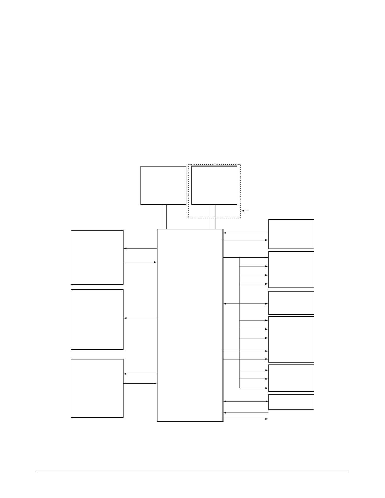
The main circuit board consists of a Jupiter-2 Chip (KS32C6500), memory, TX- and RX-related circuitry, and
some portions of the Line interface Unit, and controls the system.
7-1-2. System Control Part
This circuit consists of the EP-ROM and SRAM, External Real Time Clock crystal, RTC and memory back-up,
and the Jupiter-2 Chip (KS32C6500). The Jupiter-2 Chip is an integrated 14400bps modem, image processor, 16bit MPU, peripheral control, and analog front end circuit on a single-chip.
The modem is 14400 bps half duplex. It is a monolithic device incorporating an over sampling Σ∆ AFE, digital
filters, a digital signal processor (SDIP4) and CPU-Interface logic.
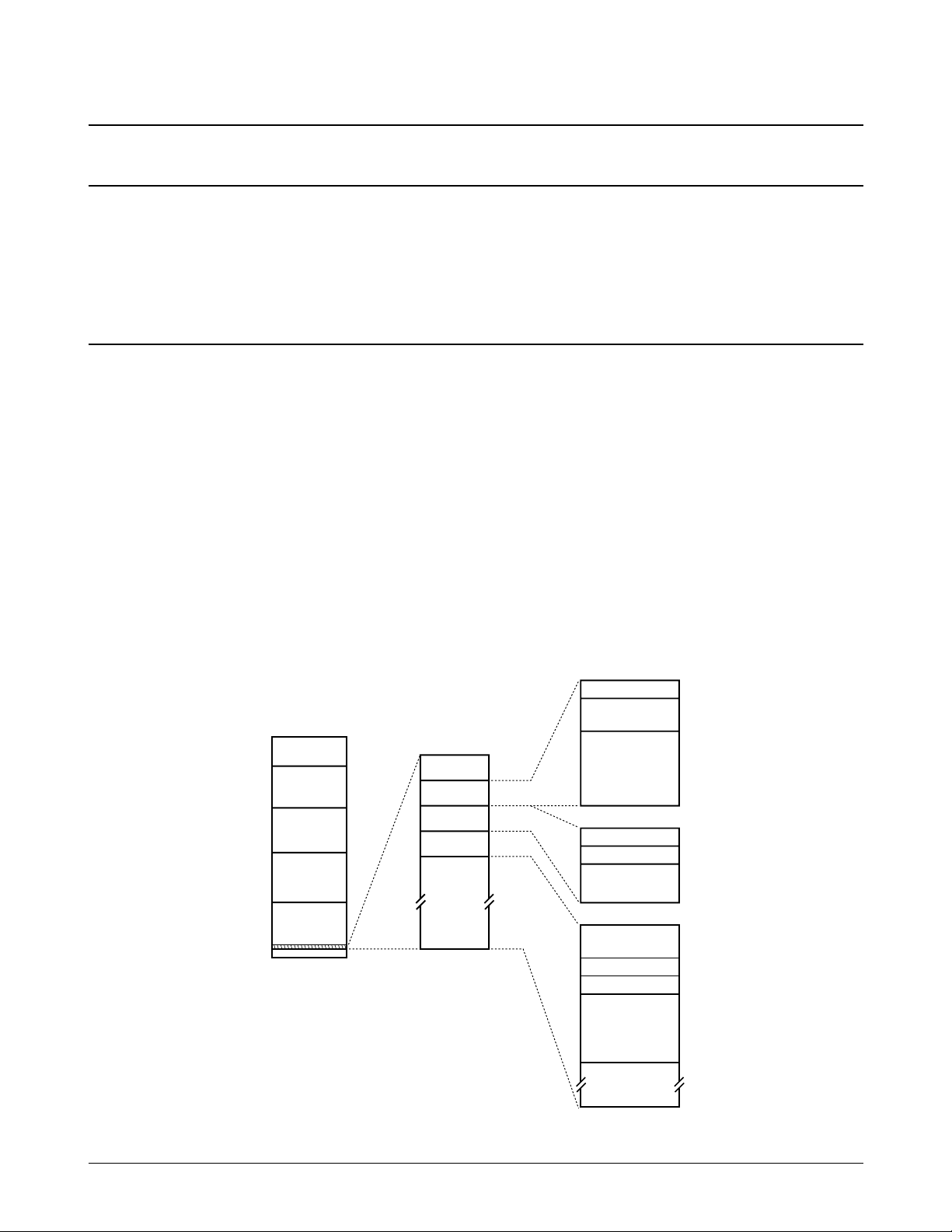
Memory Map
The external memory of the CPU is divided into 32kB RAM (0000H through 7FFFH), 512kB ROM (FC0000H
Figure 7-1 KS32C6500 External Memory Map
Samsung Electronics 7-1
Page 2
Circuit Description
OPERATING
PANEL
SERIAL
COMMUNICATION
HEAD
DRIVER
RTC
CRYSTAL
(32, 768KHZ)
SDIP4 TAD PART
KS32C6500
MOTOR
DRIVER
(CR, LF
MOTOR)
DATA
MEMORY
(SRAM)
PROGRAM
MEMORY
(EPROM)
DRAM.
(USER MEMORY)
GENERAL
PURPOSE I/ 0
TXD
A0~A5
D0~D15 D0~D7
CONTROL
RXD
PHINA~D
CONTROL
+24
XIN
ONLY SF3000T
XOUT
/DMS
/RD/WR
D0~D7
A0~A14
/RD
/LCAS
/RASO~
/UCAS
D0~D15
A0~A17
/A16
/PMS
/RD/WR
D0~D7
A0~A4
/RESET
/RESTO
MODEM
Jupiter-2 Chip
KS32C6500 internal logic generates chip select
signals for both memory chips and peripherals. To
support external access, from one to three wait
cycles can be inserted under program control during
external accesses. A chip select signal line goes
active (low) whenever its corresponding device is
accessed over the external interface. The peripheral
addresses are located in data memory.
/SRAMCS : SRAM chip select active (low)
/ ROMCS : EP-ROM chip select active (low)
D0–D15 : 16 bit data bus
A0–A17 : address bus
System Clock
The 30 MHz internal system clock frequency is
supplied by an external clock generator.
Figure 7-2 Hardware Interface Signals
7`-2 Samsung Electronics
Page 3
32.768 KHz
15 BIT
PRESCALER
1HZ CO=60 CO=60 CO=24
6 BIT
SECONDS
6 BIT
MINUTES
5 BIT
HOURS
BUSY
DETECT
5 BIT
DAYS
4 BIT
MONTHS
5 BIT
YEARS
MONTH
DECODER
LEAP YEAR
DECODER
3 STATE
DRIVER
BUSY FLAG CLEAR BUSY FLAG
CO=28,29,
30,or 31
CO=12
Circuit Description
CPU Bus
SclkCtrlLo
SclkCtrlHi
Baud Gen (8x)
Tx/Rx Control
IRQ control
SARTCmd
Internal Register
SartlRQ
SCLK
RXD
TXD
RxShift Reg
(SARTData)
RxBuffer
(SARTData)
TxShiftReg
JUPITER - 2
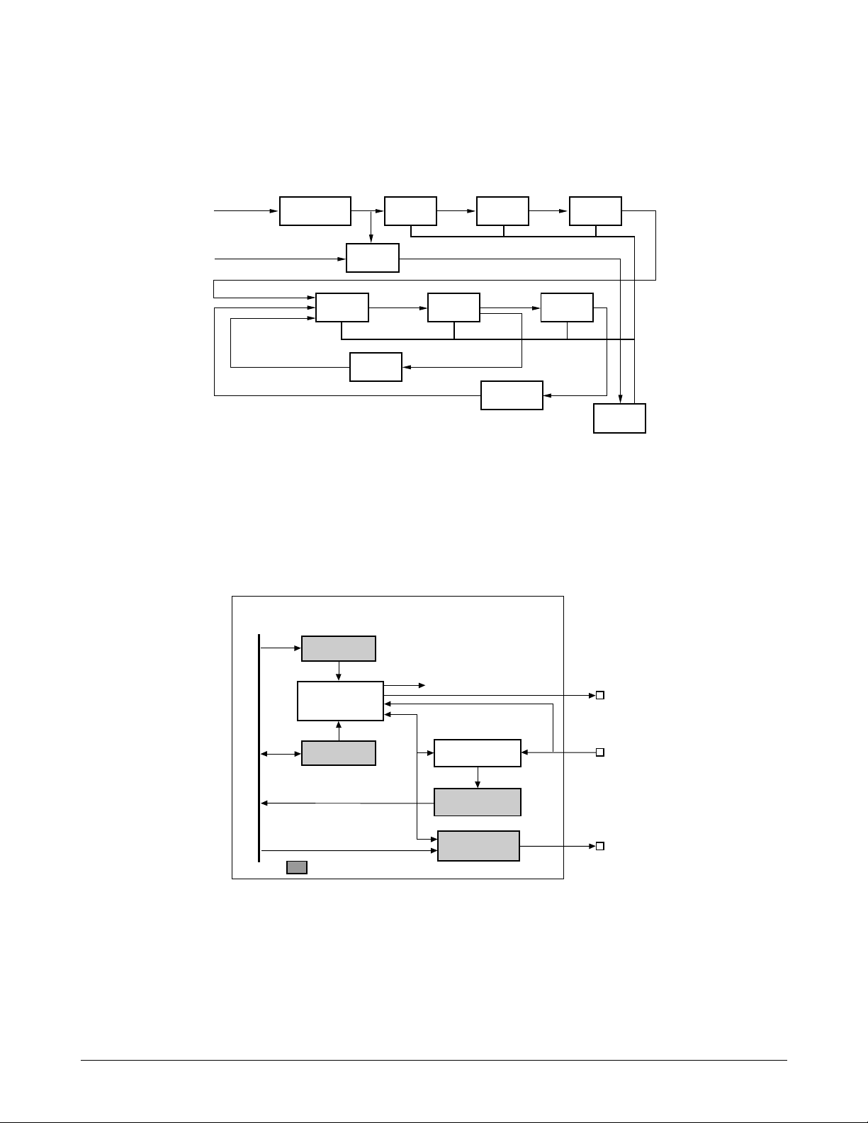
Real Time Clock (RTC)
The circuit receives clock pulses from an external 32.768 kHz crystal, which it divides into hours, minutes,
seconds, year, month, and day. A battery maintains operation when power is off. KS32C6500 can up-track 100
years, begining with 1998.
Figure 7-3 RTC Block Diagram
Operation Panel Control
A Synchronous/Asynchronous Receiver/Transmitter (SART) controls serial data transmission between the
main circuit and the operator panel.
. Serial Communication Signals
The KS32C6500 has two full-duplex serial communication ports. One port is used for I-LIU communication,
Figure 7-4 SART Block Diagram
and the other for OPE communication.
Samsung Electronics 7-3
Page 4
Circuit Description
Reset
To initialize the chip’s internal logic, the reset input
(/RESET) must be held to 0 Volt for at least 22 CPU
clocks. During this time, Vdd must be greater than 3
volt. The watchdog timer can also invoke a system
reset.
[+5V Power Monitoring]
If 5 Volt power to KIA7045P drops to between 4.65V
and 4.35V (typically 4.5V), power failure will be
indicated and the output of KIA7045P will go ‘low’
(GND5). This causes the KS16118 to become active
(‘low’=reset).
The KS32C6500 reset causes the /RESET terminal to
be reset. The output terminal of KIA7045P is an
open-drain configuration, and is connected to
KS32C6500 through a 10 kohm pull-up resistor.
Carriage Return Motor Driver
The CR motor drives the head in two directions to
print data on the recording paper.
Motor type : Step Bipolar
Operation Voltage : +24V DC
Resistance : 5 ohm +/-10%
IC : PBL3717 x2EA
STEP MOTOR DRIVER OUTPUT SIGNAL
Standby Full Step
CRIAO
CRIA 1
PHA
PHB
CRIBO
CRIB 1
500mA
IMA
-500mA
500mA
IMB
-500mA
INPUT
OUTPUT
Line Feed Motor Driver
The LF motor feeds paper in and out.
Motor type : Step Unipolar
Operation Voltage : +24V DC
Holding Voltage : +5V DC
Resistance : 50 ohm ±10%
IC : STA471A
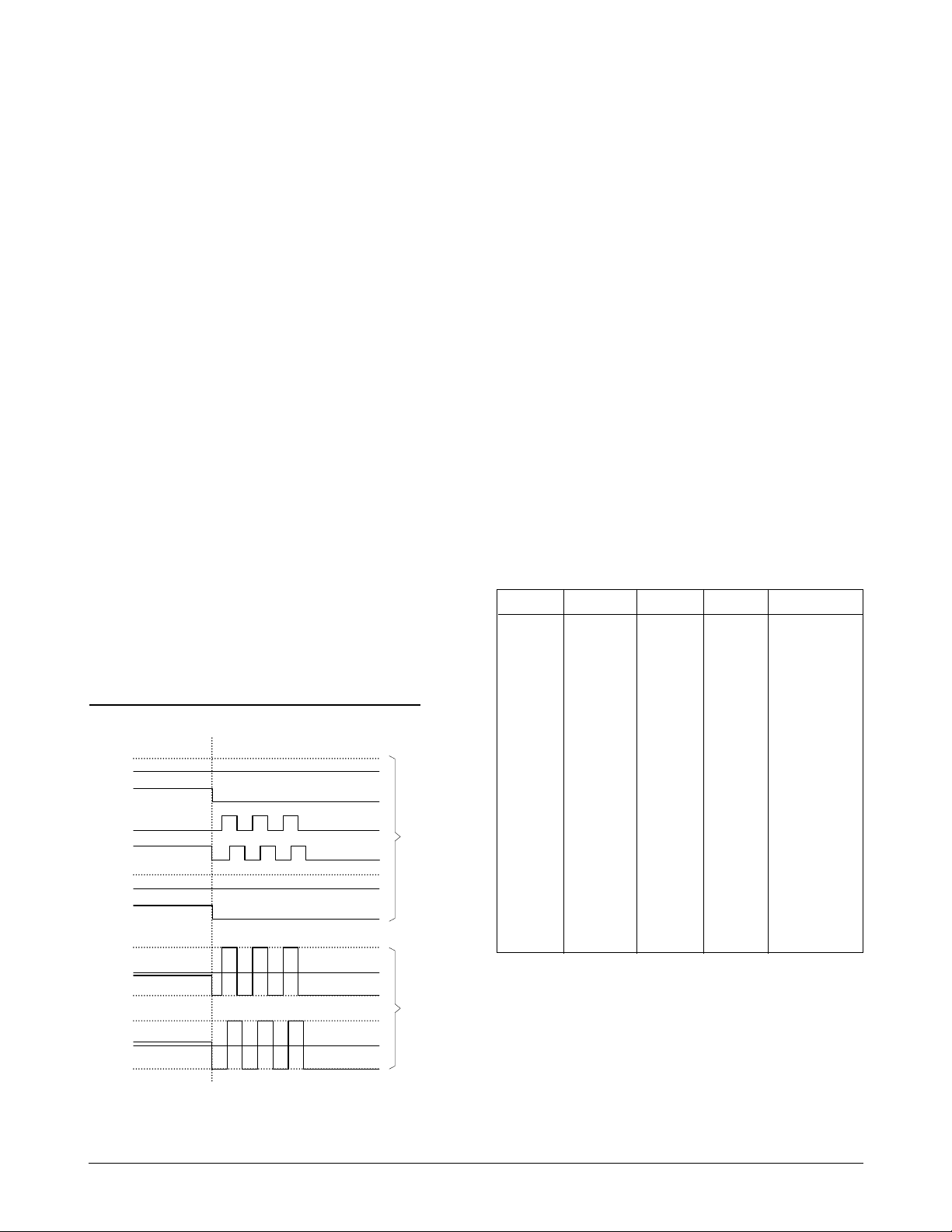
Head Nozzle Driver
The nozzle control circuit is composed as follows:
Number of nozzle : 56 nozzles for mono
Driving Voltage : +24V DC +/-2%
Driving Pulse Width : 3.6 us for mono
Operation Frequency : 5 kHz
Resistance : 30 ohm for mono
IC : SGS Thomson L6451 or Allegro A5817
The IC decodes four input signals (PHINA, PHINB,
PHINC, PHIND) and enables the selected using
OEA and OEB signal input.
IND INC INB INA N
0000 0
0001 1
0010 2
0011 3
0100 4
0101 5
0110 6
0111 7
1000 8
1001 9
1010 10
1011 11
1100 12
1101 13
1 1 1 0 ALL OFF
1 1 1 1 ALL OFF
Table 7-1 Nozzle Driver Signal
Figure 7-5 Step Motor Drive
7-4 Samsung Electronics
Page 5
1
5
10
15
20
25
30
35
40
120
115
110
105
100
95
90
85
80757065605550
45
125130135140145150155160
KS32C6500
160 QFP
(Top View)
PHADR11
PHADR10
PHADR9
PHADR8
PHADR7
PHADR6
PHADR5
GND1
HOE12
HOE11
HOE10
HOE9
HOE8
VDD1
HOE7
HOE6
HOE5
HOE4
HOE3
HOE2
HOE1
GND2
DC_CRIA0
DC_CRIA1
CRIB0
CRIB1
PORT0
PORT1
PORT2
??????????
??????????
GOP12/nHSM
HOE16/HOED?
HOE15/HOEC?
HOE14/HOEB?
HOE13/HOEA?
PHADR4/ PHIND
PHADR3/ PHINC
PHADR2/ PHINB
PHADR1/ PHINA
nECS3
nECS2
nECS1
nECS0
nWBE1
nWE
nOE
nCAS1
nCAS0
nRAS1
nRAS0
nRCS2
nRCS1
nRCS0
VDD4
VDDR21
VDDR20
VDDR19
VDDR18
VDDR17
VDDR16
VDDR15
VDDR14
VDDR13
VDDR12
VDDR11
VDDR10
VDDR9
VDDR8
VDDR7
VDDR6
VDDR5
VDDR4
VDDR3
VDDR2
VDDR1
VDDR0
GND5
nWBE0
GND6
V
D
D
3
D
A
T
A
1
5
D
A
T
A
1
4
D
A
T
A
1
3
D
A
T
A
1
2
D
A
T
A
1
1
D
A
T
A
1
0
D
A
T
A
9
D
A
T
A
8
D
A
T
A
7
D
A
T
A
6
D
A
T
A
5
D
A
T
A
4
D
A
T
A
3
D
A
T
A
2
D
A
T
A
1
D
A
T
A
0
V
D
D
2
P
P
D
0
P
P
D
1
P
P
D
2
P
P
D
3
P
P
D
4
P
P
D
5
P
P
D
6
P
P
D
7
G
N
D
3
n
S
T
R
O
B
E
n
A
U
T
O
F
D
n
S
L
C
T
I
N
n
I
N
I
T
S
E
L
E
C
T
n
A
C
K
n
F
A
U
L
T
P
O
R
T
4
P
O
R
T
3
B
U
S
Y
P
E
R
R
O
R
2
4
5
C
L
K
G
N
D
4
P
H
A
D
R
1
2
P
H
A
D
R
1
3
G
O
P
7
/
n
I
O
R
D
1
G
O
P
1
0
/
F
I
R
E
P
U
L
S
E
G
O
P
6
/
n
I
O
W
R
2
G
O
P
9
/
C
L
K
O
U
T
G
O
P
8
/
n
I
O
R
D
2
G
O
P
4
/
n
R
S
T
O
G
O
P
3
/
T
O
N
E
G
N
D
9
E
E
C
L
K
E
E
D
A
T
A
L
F
P
H
A
S
E
B
P
H
B
I
B
0
P
H
A
I
A
1
P
H
A
Z
I
A
1
P
H
B
Z
I
B
0
G
O
P
1
1
/
n
H
S
C
V
D
D
R
T
C
R
X
O
R
X
I
L
F
C
O
N
P
H
A
G
O
P
2
/
n
E
D
A
C
K
G
O
P
4
/
n
E
D
R
E
Q
G
O
P
3
/
n
E
I
N
T
2
G
O
P
2
/
n
E
I
N
T
1
G
O
P
5
/
n
I
O
W
R
1
V
D
D
5
G
N
D
8
M
C
L
K
G
N
D
7
n
R
E
S
E
T
C
L
K
S
E
L
G
I
P
5
/
U
C
L
K
T
E
S
T
2
T
E
S
T
1
G
I
P
1
/
R
X
D
2
G
I
P
1
/
R
X
D
2
G
I
P
0
/
R
X
D
1
G
I
P
0
/
R
X
D
1
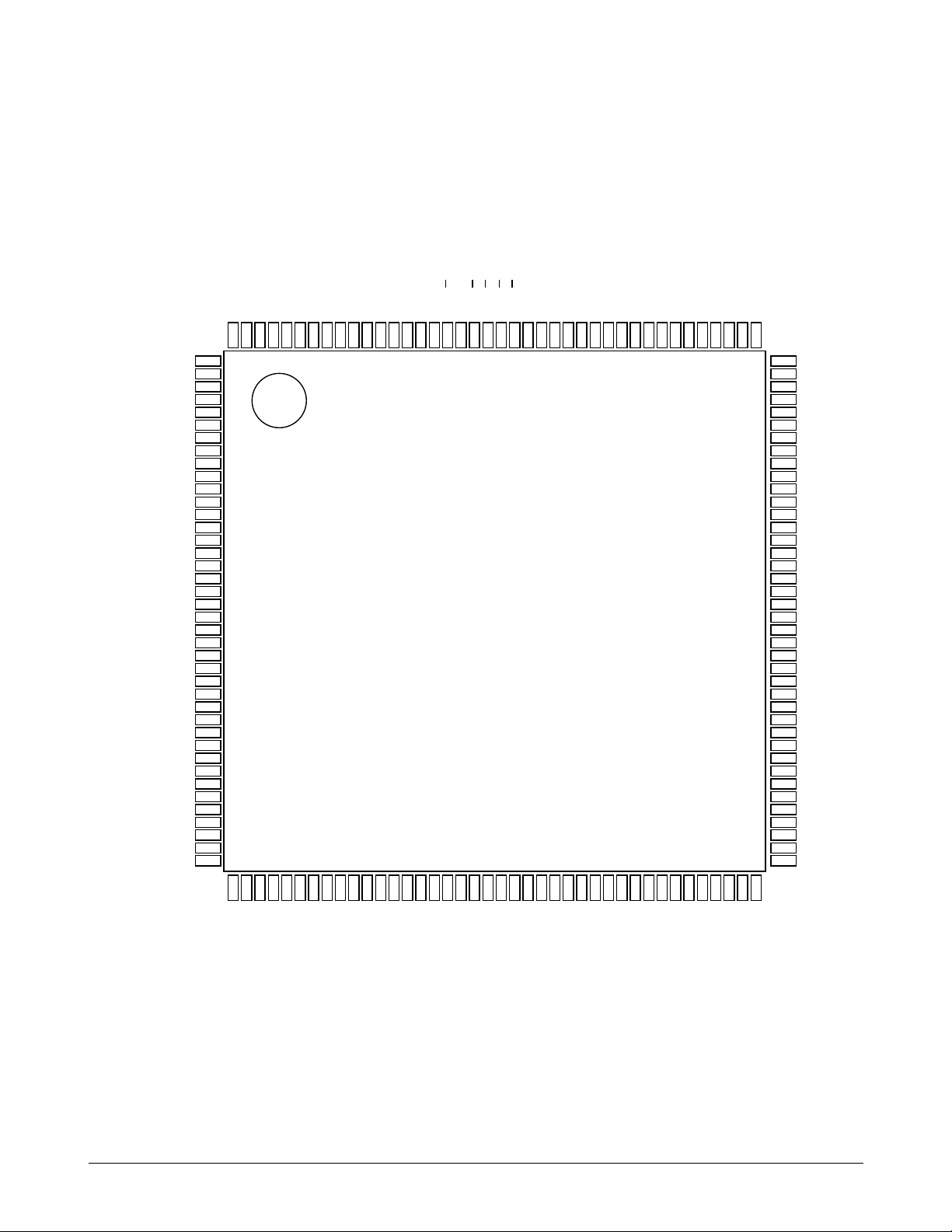
Circuit Description
Jupiter-2 (KS32C6500) Pin Layout Diagram
Samsung Electronics 7-5
Figure 7-6 Pin Layout Diagram
Page 6
Circuit Description
Jupiter-2 ASIC(KS32C6500) Pin Description
Pin No. KS32C6500 ATLAS used pin Pin Description
1 _PHGA11 NOT-USED
2 _PHGA10 NOT-USED
3 _PHGA9 NOT-USED
4 _PHGA8 NOT-USED
5 _PHGA7 NOT-USED
6 _PHGA6 NOT-USED
7 _PHGA5 NOT-USED
8 _PHGA4 PHIND INK NOZZLE ENABLE CONTROL SIGINAL
9 _PHGA3 PHINC INK NOZZLE ENABLE CONTROL SIGINAL
10 _PHGA2 PHINB INK NOZZLE ENABLE CONTROL SIGINAL
11 _PHGA1 PHINA INK NOZZLE ENABLE CONTROL SIGINAL
12 GND1 GND1
13 PHOE16 _HOED INK NOZZLE DECODING SIGNAL
14 PHOE15 _HOEC INK NOZZLE DECODING SIGNAL
15 PHOE14 _HOEB INK NOZZLE DECODING SIGNAL
16 PHOE13 _HOEA INK NOZZLE DECODING SIGNAL
17 PHOE12 NOT-USED
18 PHOE11 NOT-USED
19 PHOE10 NOT-USED
20 PHOE9 NOT-USED
21 VDD1 VDD1
22 PHOE8 NOT-USED
23 PHOE7 NOT-USED
24 PHOE6 NOT-USED
25 PHOE5 NOT-USED
26 PHOE4 NOT-USED
27 PHOE3 NOT-USED
28 PHOE2 NOT-USED
29 PHOE1 NOT-USED
30 GND2 GND2
31 GOP12 GOP12 TX CONTROL
32 DC_CRIA0 CRIA0 CRPHA, CRPAB: PHASE A, B DIRECTION
33 CRPHA/CHX CRPHA CONTROL SIGNAL
34 DC_CRI41 CRIA1 CRIA, CRIB: PHASE A, B CURRENT CONTROL
35 CRIB0 CRIB0 SIGNAL
36 CRPHB/CHY CRPHB L L : HIGH H L : MEDIUM
37 CRIB1 CRIB1 L H : LOW H H : NO
38 GPIO0 GPIO0
39 GPIO1 GPIO1
40 GPIO2 GPIO2
41 GPIO3 GPIO3
42 GPIO4 GPIO4
43 _FAULT NOT-USED
7-6 Samsung Electronics
Page 7

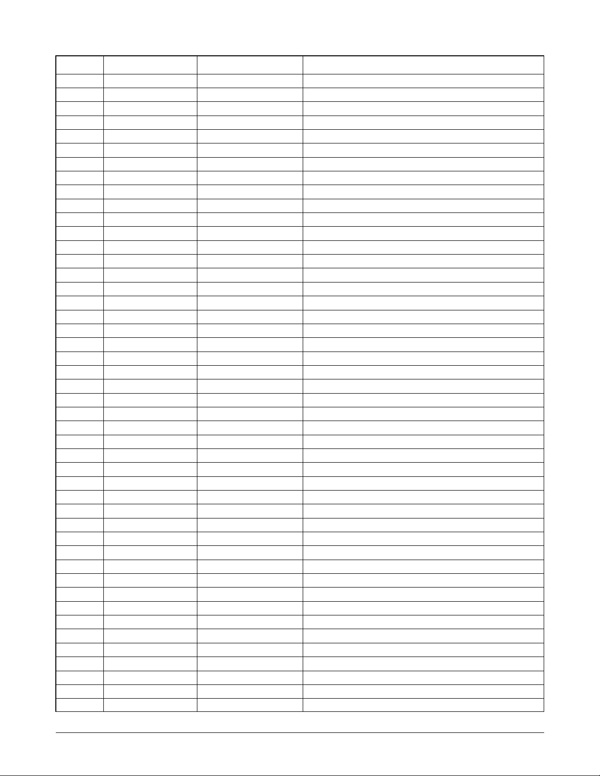
Pin No. KS32C6500 ATLAS used pin Pin Description
44 PERROR NOT-USED
45 BUSY NOT-USED
46 _ACK NOT-USED
47 SELECT NOT-USED
48 _INT NOT-USED
49 _SLCTIN NOT-USED
50 _AUTOFD NOT-USED
51 _STROBE NOT-USED
52 GND3 GND3
53 PPD7 NOT-USED
54 PPD6 NOT-USED
55 PPD5 NOT-USED
56 PPD4 NOT-USED
57 PPD3 NOT-USED
58 PPD2 NOT-USED
59 PPD1 NOT-USED
60 PPD0 NOT-USED
61 245DIR NOT-USED
62 VDD2 VDD2
63 D0 D0
64 D1 D1
65 D2 D2
66 D3 D3
67 D4 D4
69 D5 D5
69 D6 D6
70 D7 D7
71 GND4 GND4
72 D8 D8
73 D9 D9
74 D10 D10
75 D11 D11
76 D12 D12
77 D13 D13
78 D14 D14
79 D15 D15
80 VDD3 VDD3
81 A0 A0
82 A1 A1
83 A2 A2
84 A3 A3
85 A4 A4
86 A5 A5
87 A6 A6
89 A7 A7
89 A8 A8
Circuit Description
Samsung Electronics 7-7
Page 8
Circuit Description
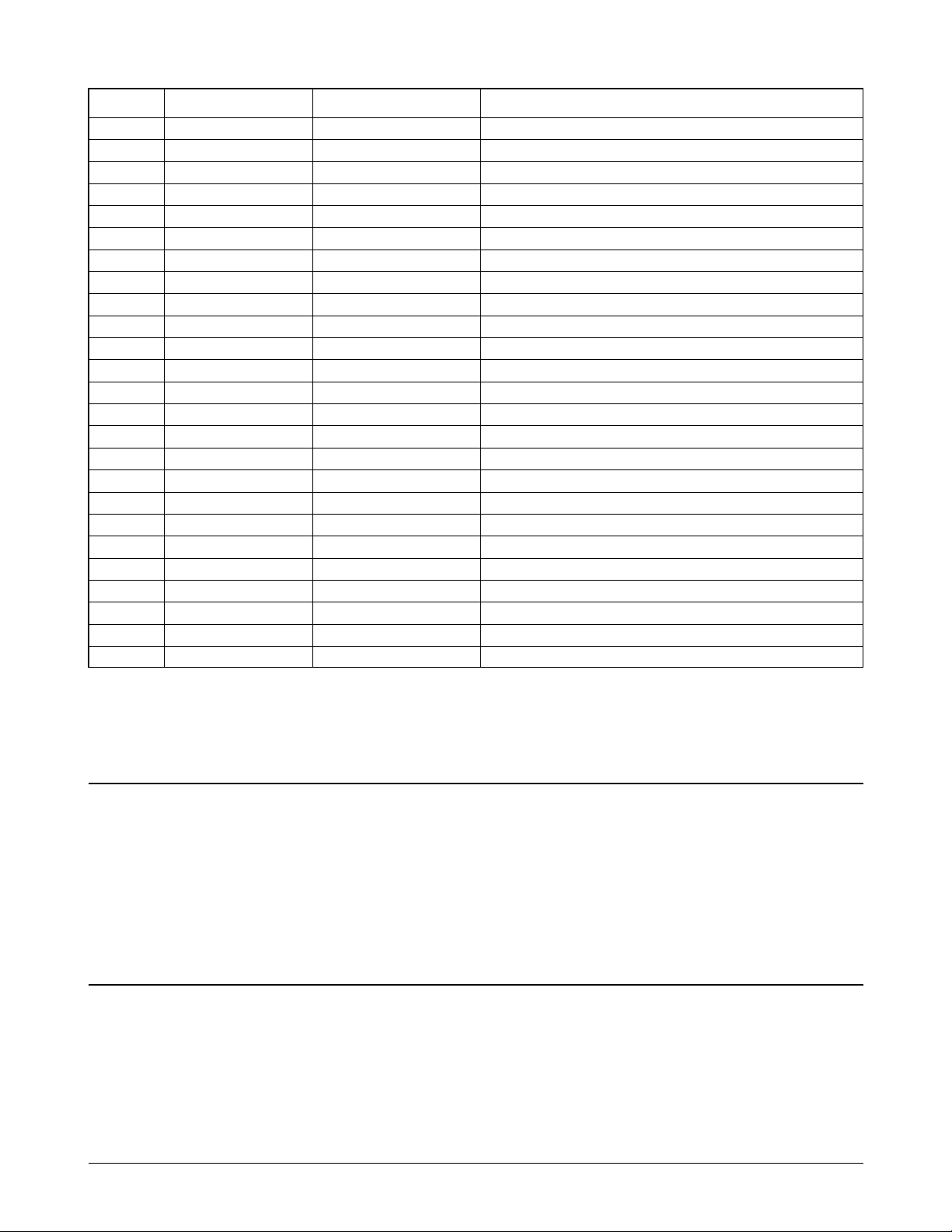
Pin No. KS32C6500 ATLAS used pin Pin Description
90 A9 A9
91 A10 A10
92 GND5 GND5
93 A11 A11
94 A12 A12
95 A13 A13
96 A14 A14
97 A15 A15
98 A16 A16
99 A17 A17
100 A18 A18
101 A19 A19
102 A20 A20
103 A21 A21
104 VDD4 VDD4
105 _RCS0 _RCS0 PROGRAM ROM CHIP SELECT
106 _RCS1 NOT-USED FONT ROM CHIP SELECT
107 _RCS2 _RCS2 SRAM CHIP SELECT
108 _RAS0 _RAS0 DRAM ROW ADDRESS STROBE (DEFAULT)
109 _RAS1 NOT-USED DRAM ROW ADDRESS STROBE (OPTION)
110 _CAS0 _CAS0 DRAM LOWER COLUMN ADDRESS STROBE
111 _CAS1 _CAS1 DRAM UPPER COLUMN ADDRESS STROBE
112 _OE _OE MEMORY OUTPUT ENABLE
113 _WE _WE MEMORY WRITE ENABLE
114 GND6 GND6
115 _WBE0 _WBE0 WRITE BYTE ENABLE
116 _WBE1 NOT-USED WRITE BYTE ENABLE
117 _ECS0 _ECS0 MODEM CHIP SELECT
118 _ECS1 _ECS1 DSP CHIP SELECT
119 _ECS2 _ECS2 SDIP4 CHIP SELECT
120 _ECS3 NOT-USED
121 GOP0 GOP0 LIU TXD
122 GIP0 GIP0 LIU RXD
123 GOP1 GOP1 OPE TXD
124 GIP1 GIP1 OPE RXD
125 TEST1 TEST1 NORMAL MODE: GND
126 TEST2 TEST2 DEBUG MODE: VCC
127 CHIP5 CHIP5 HEAD CHECK
128 CLKSEL CLKSEL MASTER CLK SELECT: H
129 _RESET _RESET SYSTEM RESET
130 GND7 GND7
131 MCLK MCLK MASTER CLK (30MHZ)
132 GND8 GND8
133 GOP5 GOP5 RX CONTROL
134 VDD5 VDD5
135 GIP2 GIP2 _MODEM INTERRUPT REQUEST
7-8 Samsung Electronics
Page 9
Pin No. KS32C6500 ATLAS used pin Pin Description
136 GIP3 GIP3 TX INT
137 GIP4 GIP4 _XDREQ (SDIP4)
138 GOP2 GOP2 _XDACK (SDIP4)
139 LFIA0 LFIA0 LF MOTOR PHASE CONTROL
140 LFPHA LFEN LF MOTOR ENABLE
141 LFIA1 LFIA1 LF MOTOR PHASE CONTROL
142 LFIB0 LFIB0 LF MOTOR PHASE CONTROL
143 LFPHB NOT-USED
144 LFIB1 LFIB1 LF MOTOR PHASE CONTROL
145 EEDATA NOT-USED
146 EECLK NOT-USED
147 GND9 GND9
148 GOP3 GOP3 KEY CLICK
149 GOP4 GOP4 POR CONTROL
150 GOP8 NOT-USED
151 GOP9 GOP9 SDIP4 CLK (30MHZ)
152 GOP10 GOP10 _RESET OUT
153 GOP11 NOT-USED
154 GOP6 NOT-USED
155 GOP7 NOT-USED
156 VDDRTC VDDRTC RTC BACK-UP
157 RXI RXI RTC CLK IN
158 RXO RXO RTC CLK OUT
159 _PHGA13 NOT-USED
160 _PHGA12 NOT-USED
Circuit Description
7-1-3. Memory
System memory consists of 512 kB ROM, 32 kB SRAM and 1024 kB DRAM. All of SRAM is backed up. ROM
and SRAM are selected by chip select lines, and data is accessed by the units position of the byte.
5V power is applied to SRAM through VSB. This facsimile machine uses a Lithium battery for memory backup.
A, 820 ohm resistor in series with the positive battery terminal is for battery protection.
7-1-4. Modem and TX- and RX- Related Circuits
These circuits control transmission between the internal MODEM and the LIU or a remote MODEM.
The KS16117 is a single-chip fax-MODEM having features to detect and generate DTMF tones. TX OUT is the
MODEM output port, and RX IN is the input port. /PORI is the Jupiter-2 signal which enables MODEM
initialization at system power on. D0 - D7 are data buses. RS0 - RS4 are internal register select signals which
determine the mode. /CS is the chip select signal, and /RD /WR are the read and write control signals. RLSD
is used for v.24 interface-related signals and /IRQ is the MODEM interrupt.
Samsung Electronics 7-9
Page 10

Circuit Description
DATA MEMORY
CPU
DMA Controller
SCAN/ MOTOR
DRIVER
IMAGE
PROCESSOR
HALF FLASH ADC
SCANNER
DOCUMENT IMAGE
ADDR-BUS
DATA-BUS
ADDR-BUS
DATA-BUS
CLK_NINE
CLK_PIX
LINE_PERIOD
AGC_PERIOD
ADSAMPLE
SI
CLKI
CLKI_
ΦR
Tx_A_Tx_B_Tx_A_Tx_B_
T
R
D
M
A
A
C
K
T
R
D
M
A
R
E
Q
B-BIT
VIDEO SIGNAL
(analog)
[SDIP4]
Transmit Circuit
This circuitry controls transmission of analog signals
from the MODEM. Output voltage from the
MODEM is buffered through the LIU board and OP
Receive Circuit
In receive mode, analog signals from the LIU board
are transferred to RX IN through the BPF and
smoothing filter.
amp after signal smoothing and filtering, and finally
output to the line.
7-1-5. Image Processor / Motor Driver (SDIP4)
• Scan driver generates the control signals to acquire the document data from the scanner and to operate the
Image Processor.
• Motor driver generates the control signals to drive the Tx-Motor according to programmed motor speed.
Figure 7-7 Block Diagram of Scanner Control Function
7-10 Samsung Electronics
Page 11

Circuit Description
AGC MODULE
(A/D, D/A I/F)
A/D data[7:0]
Initial Data[7.0]
CPU
I/F
MODULE
(Register Files)
SHADING
CORRECTION
MODULE
GAMMA
CORRECTION
MODULE
DECIMATION/
INTERPOLATION
MODULE
EDGE-
ENHANCEMENT
/EMPHASIS
MODULE
ERROR-
DIFFUSION
MODULE
[IMAGE - PROCESSOR]
Image Data
Memory
I/F
MODULE
BINARY Decision &
Output
MODULE
CPU - Data Bus[15:0]
CPU - Addr Bus[26:0]
CPU - read
CPU - write
IP_CS_
RAM - Data Bus[7:0]
RAM - Addr Bus[14:0]
RAM _read_
RAM _write_
Tr_DMA_request
Tr_DMA_acknowledge
pclk
pdata
ERM-Mode
Edge-Strength
Half-Tone enable
Vpeak_IN[7:0]
Vpeak_OUT[7:0]
Gamma Corrected Value[7:0]
Shading Factor[7:0]
Shade Corrected Value[7:0]
Gamma Corrected Value[7:0]
ERM_Data[7:0]
Edge_Data[7:0]
Error-Diffused Data[7:0]
Figure 7-8 Hardware Block Diagram of Image Processor
HARDWARE BLOCK DIAGRAM
Samsung Electronics 7-11
Page 12

Circuit Description
500 KHZ (L:DUTY 75%)
SI
CLOCK
SIG
1 LINE
Image Sensor
This shading wave is formed by scanning the white roller prior to a document. The slice level is determined by
the shading wave, and compensates for shading distortion according to the CIS characteristics. The wave
format from the CIS is converted into a 6 bit digital value in the SDIP4 image processor, and then processed in
B/W or intermediate mode.
CIS Driver
The CIS driver clock (CLK) frequency is 500
kHz. A low duty cycle of 75% is used to
lengthen the charging time. Astart signal (SI) is
provided every 5 ms to match the line scanning
time. Actual image signal (VIN) is provided in
less than 3.4 ms, using the 500 kHz clock,
taking A4 paper size into consideration.
Figure 7-9 CIS Diver Clock Timing
Sensor Detection Circuit
PE SENSOR 1,2
This sensor detects whether paper is loaded in the automatic sheet feeder. If no paper is detected, the output
signal turns high. While paper is feeding to print, the output turns low.
HOME DETECTION CIRCUIT
This circuit detects whether the head is in home position. When power turns on and head is capped, the circuit
is activated. If the head is in the home position, the output turns high.
Scan Motor Controller
The SF3000/SF3000T model facsimile machines perform their send function utilising a single 24 volt motor.
This motor has a winding resistance of 120 ohms. Three drive strobe pulses are used to operate the motor.
Motor Function Drive Strobe Pulse Phase
Document Feed In/Out 400 pps 1-2 phase
Fine Copy/Tx 400 pps 1-2 phase
Super Fine Tx 400 pps 1-2 phase
7-12 Samsung Electronics
Page 13

SDIP4 Pin Layout Diagram
SDIP4
144-QFP
1
2
3
4
5
6
7
8
9
10
11
12
13
14
15
16
17
18
19
20
21
22
23
24
25
26
27
28
29
30
31
32
33
34
35
36
108
107
106
105
104
103
102
101
100
99
98
97
96
95
94
93
92
91
90
89
88
87
86
85
84
83
82
81
80
79
78
77
76
75
74
73
/RESET
D15
D14
D13
D12
D11
D8
D7
D6
D5
D4
D3
D2
D1
D0
D10
D9
VDD
VSS
VDD
VSS
VDD
VSS
GPI0
GPIO0
GPIO1
GPO0
GPI1
GPIO2
GPIO3
GPO1
VDD
VSS
VSS
VSS
VSS
GPO5
GPO4
GPIO9
GPIO8
AA14
AA13
AA12
AA11
AA10
AA9
AA8
AA7
AA6
AA5
AA4
AA3
AA2
AA1
AA0
GPI4
GPI5
VSSA
VDDA
VREFDAC
VREFADC
ADCIN
VSS
VSS
VSS
VDD
VDD
VSS
VSS
VSS
VDD
VSS
109
110
111
112
113
114
115
116
117
118
119
120
121
122
123
124
125
126
127
128
129
130
131
132
133
134
135
136
137
138
139
140
141
142
143
144
72
71
70
69
68
67
66
65
64
63
62
61
60
59
58
57
56
55
54
53
52
51
50
49
48
47
46
45
44
43
42
41
40
39
38
37
VDD
VSS
VSS
VSS
VDD
VSS
VSSA5A4
A3
A2
A1
A0
IPCS_
VSS
CLKI
/CLK
/SH
/WR
/RD
GPIO14
GPIO15
GPO7
ADCCLK
VSS
GPI6
GPIO10
GPIO11
GPO6
Tx_A
Tx_B
Tx_B
Tx_en1
Tx_en2
Tx_int
Tx_A
VSS
VSS
VSS
VSS
DD0
DD1
DD2
VDD
VDD
VDD
VDD
VSS
VSS
VSS
VSS
XCLK
VSS
VDD
/RAMWR
/RAMRD
GPO3
GPO2
GPIO7
GPIO6
GPIO5
GPIO4
GPI3
GPI2
GPI7
GPIO12
GPIO13
DD3
DD4
DD5
DD6
DD7
Circuit Description
Figure 7-10 Pin Lay out Diagram
Samsung Electronics 7-13
Page 14

Circuit Description
SDIP4 ASIC Pin Description
Name Type Description
RESET I Power on reset pin. active : L
A[5:0] I CPU interface address bus.
D[15:0} B CPU interface data bus.
WR I CPU interface write signal pin.
RD I CPU interface read signal pin.
IPCS I CPU interface chip select signal pin.
XP I System clock input pin.
AIN I Sensor image signal input pin.
Ør O CCD charge clear signal pin.
SI O CCD/CIS line clear signal pin.
CLK1 O Sensor Drive signal output pin.
CLK2 O
DREQ O DMA data request signal output pin. active : H
DACK I DMA data acknowiedge output pin. active : L
RAM_RD O IP-SRAM read signal pin.
RAM_WR O IP-SRAM write signal pin.
RAM_addr[14:0] O IP-SRAM address bus.
RAM_data[7:0] O IP-SRAM data bus.
Tx_A O
Tx_B O
Tx_A O Motor drive signal pins.
Tx_B O
Tx_en1 O
Tx_en2 O
Tx_int O Motor drive interrupt pin.
GPI[7:0] I General purpose input pins.
GPO[7:0] O General purpose output pins.
GPIO[7:0] B General purpose input/output pins.
7-14 Samsung Electronics
Page 15

7-1-6. TAD (SF3000T Only)
TAD circuit consists of a voice coprocessor to record and play voice messages in voice memory.
Circuit Description
Recording path
R62 provides power to the condenser microphone.
Voice signal from the microphone is passed through
active filter U22, R60 and C51, R58, C48 to clear
aliasing noise occuring while sampling and
amplifying the signal. Q5 and Q4 compose ALC
(Automatic Level Control) circuit. CODEC (U29)
converts the voice signal to digital and converts the
digital signal from voice coprocessor into analog for
line output.
Mic input path
Transmit path functions as MIC input path.
Outgoing messages and memo messages from
CODEC are stored in the voice memory (4Mb
DRAM) through the DSPG DRAM controller.
Line input and play path
Incoming signals from line are stored in the voice
memory (4Mb DRAM) through CODEC and DSPG
DRAM controller. When played, DSPG processes
the data stored in voice memory and sends it out to
LIU through CODEC and R93. To playback through
the speaker, DSPG sends the signal to speaker
through R93, MUX (U25, U26), and op amp.
DSPG
This circuit consists of Host Interface, Memory
Interface, CODEC Interface, and DSP core. Host
Interface sends and receives data to and from IFC.
Memory Interface sends and receives the
compressed voice data to and from DRAM to play
back and record voice data. DSP core communicates
with host IFC through Host Interface.
Voice backup
+5V is supplied for voice memory through VBT
when power is on. When power is off, +5V is
supplied from the 9V backup battery.
Samsung Electronics 7-15
Page 16

Circuit Description
7-1-7. LIU PBA
The LIU (Line Interface Unit) interfaces the MODEM and telephone to the telephone line. The FAX and
telephone portions of the LIU are active with machine power on. When machine power is off, only the
telephone circuity operates, powered by telephone line voltage. The FAX portion of LIU consists of the interface
between MODEM and telephone line, and the circuits for DC loop feeding, DP signal, loop current and ring
detect. The telephone portion is divided into ringer, dialling and speech circuits. Refer to the schematic and
connection diagram sections of this manual.
FAX section
MODEM/LINE INTERFACE
Following is the path for data and remote control
signals:
• CML1 relay: Switches telephone line between FAX
and telephone circuits.
• U1 pin 3TIT: Single ended input for transformer
(T2)
TIT: Transformer Input from Transformer
• U1 pin 40 ROT: Output for driving transformer
(T3) with an AC impedance greater than 10 Kohm.
ROT: Receive Output Transformer
• C57: DTMF and CNG detect path to T1 20Kohm
winding under idle conditions, and DC blocking
for 20Kohm winding.
• AC impedance: The AC impedance of U1 (I-LIU)
is set to 1000 ohm by external capacitor (C32) at
U1 pin 8 CI (Complex Impedance Input) port.
With the external resistor (R38) at U1 pin 34 ACI
port, it can be programmed to 600ohm. U1 pin 35
CS (Current Shunt control output) port is an
N-channel open drain output to control the
external high power shunt transistor for
synthesizing AC and DC impedance.
• DC conditions: The normal operating mode is
from 15mA to 100mA. An operating mode with
reduced performance is from 5mA to 15mA. In the
line hold range from 0mA to 5mA, the device is in
a power down mode and the voltage at U1 pin 37
LI (Line Input) port is reduced to a maximum of
3.5V. The DC characteristic is determined by the
voltage at U1 pin 37 LI port and R45 resistor
between U1 pin 37 LI and pin 39 LS port. It can be
calculated by the following equation: V
LINE X 45.
I
LS = VLI +
RING DETECT
• U1 pin 28 (MO) is ring melody output port and
this signal drives FET3 which drive Photo coupler
U4 for artificial ring.
MF DIAL
• U1 pin 2 DMS (Dial Mode Selection) port is set to
VDD by R46. It has M/B ratio of 33:66, and in no
power operation mode operates only DP.
• MF signal appears (tone level of low group:
typical - 14 dBm) at U1 pin 4 MFO (DTMF
Generator Output). This signal is leveled by R32,
R28 and C29, then to amplier U1 pin 9 MFI
(DTMF Amplier Input).
• Line dial signals appear at U1 pin 39 LS (Line
Current Sense Input).
(Same as telephone section)
DP DIAL (Same as telephone section)
• U1 pin 2 (DMS) is set to Vdd (33/66) or VSS
(40/60) by R46 or R52 resistor.
• Dial pulses originate at U1 pin 27 (DPN), which
toggles Q5, which drives Q2. The resulting
intermittent voltage interrupts the telephone line.
• Pulse M/B ratio is set by U1 pin 2 DMS port.
Vdd = 33/66, and Vss = 40/60.
• U1 pin 35 CS port: Modulation of line voltage and
shorting the line during make period of pulse
dialling.
7-16 Samsung Electronics
Page 17

LLC (Line Loss Compensation) LOOP
CURRENT DETECT
Circuit Description
• The LLC is a pin option. When it is activated, the
transmit and receive gains for both I/O are
decreased by 6dB at line currents from 20mA
when the U1 pin 31 LLC is connected to AGND,
from 75mA when this pin is connected to VDD.
The LLC is deactivated when LLC pin is
connected VSS.
• When the CML1 relay or Hook Switch switches to
telephone line, the U1 in the LIU board and CPU
(U1) in the Main board srart communication. The
U1 send <Ack> message contains the line current
information. Using this line current information
Main CPU can recognize a parallel phone.
SERIAL
• U1 pin 11 RXD: Schmitt trigger input (treshold =
• U1 pin 29 TXD: Open drain output from serial
• The communication principle is derived from a
INTERFACE
2.5V) to serial interface.
interface.
standard UART:
Baud Rate 9600
Start Bit 1
Stop Bit 1
Data Bits 8
Parity Bit None
LSB is transferred prior to MSB.
Telephone Section
• Line ring voltage passes through bridge diode
BD1, CML relay and Hook Switch to FET3 (BS170)
pin 3, C21, R19.
• The ring frequency discriminator of U1 assures
that only signals with a frequency between 13Hz
and 70Hz are regarded as valid ring signals.
• When a valid ring signal is present for 73ms
continuously, the ring melody generator (pin 28,
MO) is activated and remains active as long as a
valid ring signal is present.
• U1 filters the ring signals and output is pin 28
(MO).
• The 3 basic melody frequencies are : F1 = 880 Hz,
F2 = 1067 Hz and F3 = 1333 Hz. The repetition
rate is set to 4 which means that the sequence of
F1, F2, F3, F1, F2, F3 is repeated 4 times within a
second.
SPEECH CIRCUIT
• U1 (STI9510) and associated components.
• Handset transmitting circuit. Condensor MIC of
handset is filtered by R25, C28, C27, C20, C19,
C24, C22 and C30, and then amplified by U1 pin
32 and 33 (M1, M2)
• Handset receiving circuit. Receiving (Dynamic
unit) of handset is filtered by R49, C45, C40, C44
and C23, and then applied by U1 pin 1 (ROH) and
VSS.
• U1 pin 39 (LS) is audio output to telephone line.
RINGER CIRCUIT
SIDETONE CIRCUIT
• When a ringing signal is applied to the line, Vdd
of U1 (I-LIU) is charged up via an external path.
After Vdd has reached the operating voltage the
oscillator starts and U1 discriminates the ring
frequency.
After a valid ring frequency is applied to the U1
pin 25 RFD (Ring Frequency Discrimination) port,
the ring melody generator of U1 sends out a 3tone melody via the U1 pin 28 MO (Ring Melody
Output)port.
• U1: I-LIU and associated components.
• Ring frequency passes through DC blocking
capacitor C3 or C4 (for Switzerland or Austria)
and Zener-diode ZD2 or ZD3 (for Switzerland or
Austria) to U1 pin 25 RED port.
Samsung Electronics 7-17
• Sidetone audio characteristics are controlled by
R37, R51, R5, R26, and C41 connected to U1 pin 7
STB.
Page 18

Circuit Description
Document
Detect
Sensor
Connector
MICOM
Z-8601
LCD
16 x 1 lines
Key Matrix
LEDs
1 (SF3000T
Only)
8
Y
X
7
11
2
UART
Reset
7-1-8. OPE PBA
OPE PBA consists of U300 (MICOM Z8601), LCD, key matrix, LED indicators, and the document detect and
scan position sensors. Refer to OPE Schematic Diagram and Wiring Diagram sections of this manual.
• Signals from the key matrix and delivered to U300 X/Y input pin group (P1-X).
• U300 pin 4 (RX DATA) is UART code to MAIN PBA.
• Display from controller is received at U300 pin 5 (TX DATA).
• LCD drive signals are U300 P2-X pin group, connector pin P303-1 ~ P303-3.
• Machine status LED drive signals are U300 P01 pin group. (SF3000T only)
• Connector P302 is NPO (No Power Operation) key matrix output.
7-18 Samsung Electronics
Figure 7-11 OPE Block Diagram
Page 19

7-2. Block Diagram
MMAAIINN
MMIICC__AAMMPP
MMEEMMOORRYY
DDSSPPGG
((66330055BB))
PPIICCKK
UUPP
SSEENNSSOORR
SSDDIIPP44
**IIMMAAGGEE__RROOCCEESSSSOORR
**TTxx__MMOOTTOORRCCTTLL
**GGPPII,,GGPPOO,,GGPPIIOO
IIMMAAGGEE
MMEEMMOORRYY
MMEEMMOORRYY
**EEPPRROOMM
**DDRRAAMM
**SSRRAAMM
CCPPUU
KKSS3322CC66550000
WWAATTCCHHDDOOGG GGPPOO,,GGPPII,,GGPPIIOO
RREEAALLTTIIMMEECCLLKK CCRRMMOOTTOORRCCTTLL
SSAARRTT((LLIIUU)) LLFFMMOOTTOORRCCTTLL
SSAARRTT((OOPPEE)) HHEEAADDCCOONNTTRROOLL
AAFFEE
MMOODDEEMM
((KKSS1166111177))
MMOOTTOORR
DDRRIIVVEERR
((TTXX,,CCRR,,LLFF))
HHEEAADD
DDRRIIVVEERR
((AA55881177SSEEPP))
LLIINNEE
EE__PPHHOONNEE
HH AANNDDSSEETT
HHOOOOKK
SS//WW
LLIIUU
IILLIIUU
((SSTTII99550011))
C
O
L
1
4
R
O
W
1
4
TxD/RxD
MODEMTx/R
x
+
2
4
V
1
2
V
+
5
V
G
N
D
5
G
N
D
1
2
G
N
D
2
4
PPOOWWEERRSSUUPPPPLLYY
AC
POWER
MMIICC
SSPPEEAAKKEERR
CCIISS
CCRR
MMOOTTOORR
LLFF
MMOOTTOORR
PPEEMMPPTTYYSSEENNSSOORR
HHEEAADD
LLCCDD
OPE_RST
OOPPEE
MMPPUU
((ZZ88660011))
DDDDEETT
SSEENNSSOORR
DDSSCCAANN
SSEENNSSOORR
OPE_TxD/RxD
TT XX
MM OO TT OO RR
Samsung Electronics 7-19
Page 20

7-3 Schematic Diagrams
7-3-1. Main Circuit Diagram
CPU
7-20 Samsung Electronics
Page 21

Schematic Diagrams
SCAN, I/O
Samsung Electronics 7-21
Page 22

Memory, Motor
Schematic Diagrams
7-22 Samsung Electronics
Page 23

Schematic Diagrams
Modem
Samsung Electronics 7-23
Page 24

DSPG
Schematic Diagrams
7-24 Samsung Electronics
Page 25

Schematic Diagrams
Head Driver
Samsung Electronics 7-25
Page 26

Connector
Schematic Diagrams
7-26 Samsung Electronics
Page 27

Schematic Diagrams
E
D_DET
D0
D_SCAN
D1
D4
D5
D7
D2
D0
D1
D2
D3
RS
R_W
D6
D3
D4
D_SCAN
D_DET
D3
ANSWER
D1
D0
Only used for SF3000T
D4
D2
7-3-2. OPE Circuit Diagram
Samsung Electronics 7-27
Page 28

7-3-3. Hook Circuit Diagram
(*)SERIAL_OFF
(*)SERIAL_ON
P1-1
MHS_IN
MHS_OUT
LINE_IN
RING_OUT
EXT
LINE_OUT
RING_IN
P1-9
P1-4
P1-7
P1-8
P1-2
P1-3
P1-6
(*) IS FOR ITALY
P1-5
OFF_HOOK_STATE
Schematic Diagrams
7-28 Samsung Electronics
Page 29

Schematic Diagrams
+5V
GND5
CN1-2
CN1-3
1
2
3
4
HOME
CN1-1
7-3-4. Home Circuit Diagram
Samsung Electronics 7-29
Page 30

7-3-5. AFPS-V2 (1)
Schematic Diagrams
7-30 Samsung Electronics
 Loading...