

Page 1

Repair Manual
Repair Manual
1. Block Diagram
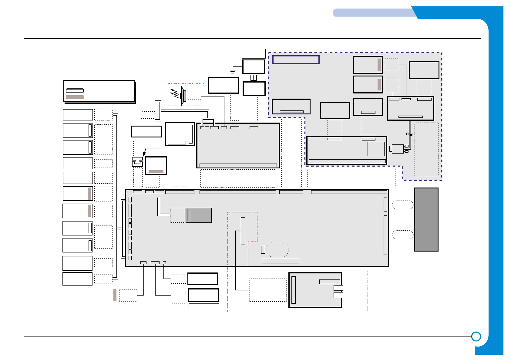
2. Connection Diagram
3. Circuit Description
4. Schematic Diagrams
CONTENTS
Digital Laser
MFP
SCX-5312F/SCX-5112
Page 2

Page 3

Samsung Electronics Digital Printing
CS Group
Copyright (c) 2001. 11
This manual is made and
described centering around
circuit diagram
and circuit description needed
in the repair center
in the form of appendix.
Page 4
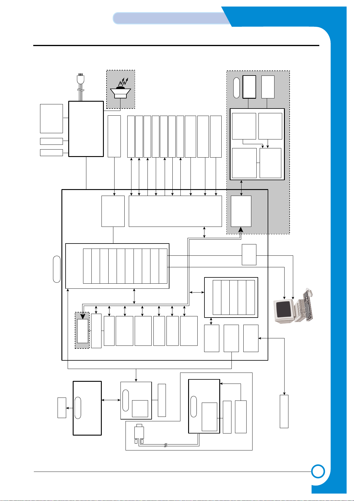
1
1-1
Samsung Electronics
BLOCK DIAGRAM
Repair Manual
1. Block Diagram
Only SCX-5312F
Only SCX-5312F
Only SCX-5312F
LCD
OPE
MICOM
- LCD Drive
- Key Scan
FLAT
D-SUB
CONN.
FLAT MOTOR
ADF
MOTOR
DRIVER
ADF MOTOR
PAPER SENSOR
POS, DET
3P X 2EA
ADF OPTION
CCD MODULE
22P
ARM7TDMI
UART * 2
MEMORY I/F
CACHE (8K)
DMA CNTR
PVC
GEU
I/O I/F
USB
IEEE1284
MOTOR
DRIVER
SW2918 / TEA3718
EXTERNAL
GPIO
74HC245
74HC273
11P
8P
2P
3P3P3P
4P4P2P
2P X 3EA
3P X 2EA
6P X 1EA
4P X 1EA
LSU
THE RMISTOR
FAN
DEV_ID
TONER_TX
TONER_RX
PTL
SOLENOID
PICK_UP, DUPLEX, MP
PAPER SENSOR
FEED+P.EMP, EXIT, MP,BIN-FULL
COVER OPEN S/W
+24V / +5V
LIU
LINE1
EXTERNAL
PHONE
TRANSFORMER
600 / / 600
TX : RX
MODEM &
EXT_PHONE
PAPER A TING
PART
EXTER NAL
PHONE
INTE RFACE
PART
LINE
INTERFACE
MODEM
33.6Kbps
14P
UNICON
USB CABLE
CENTRONICS
CABLE
Image Processor
12bit ADC
I/O PORT
Motor CNTR
DMA I/F
CIP3
FAST SRAM
(1Mbit)
MOTOR
DRIVER
CCD
I/F PART
15P D-SUB
24P
5P
RTC
Back-up Part
SRAM
(32KB)
FLASH ROM
(1MB) X 2EA
F/W
FLASH ROM
(1MB) X 2EA
PCL
DRAM
(8MB)
DRAM
(8MB)
FONT ROM
KM23C8105 H/L
PCL
SPGPe+
MAIN
24P
MOTOR 1
MOTOR 2
SMPS / HVPS
+5V/+24V/+12V/+24Vs/Fuser
T
H
V
M
H
V
DEV
SUPPLY
BLADE
Page 5
2
2-1
Samsung Electronics
CONNECTION DIAGRAM
Repair Manual
2. Connection Diagram
MAI N
FLAT
LS
U
CCD MO DUL E
THERMISTOR
D
UPLEX SOL.
DEV_I D
MP S OL.
LI U
SMPS / HVPS
1.GND_5 2. +5 V 3.
GND_5
4.+5V 5.GND_5
6. + 5V 7 .
GND_12
8.+12V 9.
GND_ 24
10.+24V 11.
GND_24
12. +24V 13.
GND_24
14. +24V 15.
THV_PWM
16 . +2 4V S 1 1 7 .
THV_EN
18. +24VS1
19.
THVREAD
20.
FUSER_ON
21.
MHV_PWM
22.SPK+ 23.
DEV_P W M
24. SPK-
1.nHSYNC
2.+5VS
3.GND_5
4.nLD_ON
5.nVDO
6.NC
7.LSU_CLK
8.nLREADY
9.PMOTOR
10. GND_24
11. +24VS1
123 45678 91011
123 456
7
8
9
1
0
1
1
1.
GND_24
2.+24V 3. +5V 4.GND_24 5.
ADF_PH A6.GND_57.ADF_I A( 1)
8.
ADF_I A( 0)9.ADF_I B(0 )
10 . A D F_ P HB11.
MODULE_DETECT
12. ADF _I B(1)
13.
ADF_P_POS14.ADF_P_DET
15.NC 16.
ADF_P_REGI
17.OPE_RXD
18.OPE_RST 19. OPE_TXD 20
.FLAT_COVER
21 . T M_A 2 2.
TM_NA
23. TM_B
24. TM_NB
123 45678 9101112131415161718192021222324
1 2 3 45 6 7 8 910 11121314 151617181920212223 24
2 1 4 36 5 8 7 109 12111413 161518172019222124 23
1,2. INV_POWER
3,4.GND_12
5.CCD_HOME
6,7. +12V
8.CCD_TG
9.GND_5
10.CCD_CLK1
11.GND_5
12.CCD_CLK2
13.GND_5
14.CCD_RS
15.GND_5
16.CCD_CP
17.GND_5
18.GND_12
19.
VOUT _
VOUT _
VOUT _
R
20. G
21. B
22. GND_12
PC
Parallel Port
36pin
USB Port
4pin
214 36587 1091211141316151817201922212423
FLAT
MOTOR
1.FLAT_A
2.FLAT_NA
3.FLAT_B
4.FLAT_NB
OPE
1.GND_5
2.+5V
3.OPE_TXD
4.OPE_RST
5.OPE_RXD
D-SUB
CONN.
15P D-SUB
ADF
1.+24V
2,3. GND_2 4
4.+5V
5.GND_5
6.ADF_PHA
7.ADF_IA( 0)
8.ADF_IA( 1)
9.ADF_PHB
10.ADF_IB(0)
11.ADF_IB(1)
12.
MODULE_DETECT
13. ADF_P
ADF_P
ADF_P
_DET
14. _POS
15. _REGI
16. NC
ADF
MOTO R
1.ADF_A
2.ADF_NA
3.ADF_B
4.ADF_NB
1.+5V
2.
SI GN AL
SI GN AL
3.GND_5
GND_5
1.+5V
2
3.
4,5. NC
SCANNER PART
DET EC T
SENSOR
SENSOR
POSI ON
EXIT
SENSOR
1.+5V
2.S IGNAL
3.GND_5
1
.
T
H
E
R
M
1
2
.
T
H
E
R
M
2
JOI N T T YP E
1
.
T
H
E
R
M
1
2
.
T
H
E
R
M
2
DC FAN
1.+24V
2.NC
3.Control
1.
MTR1
MTR1
MTR1
MTR1
MTR2
MTR2
MTR2
MTR2
_I B ( 0 )
2.
_I B ( 1 )
3.
_I A ( 0 )
4.
_I A ( 1 )
5.
_I A ( 0 )
6.
_I A ( 1 )
7.
_I B ( 0 )
8.
_I B ( 1 )
MOTOR_1
1
2
3
4
MOTOR_2
5
6
7
8
1.+24V
2.Control
1.DEV_I D1
2.NC
3.DEV_I D
RX
1.NC
2.S IGNAL
SIGNAL
SIGNAL
SIGNAL
3.GND_5
4.NC
TONER_
TONER_
TX
1.+5V
2.Control
3.NC
1.+5V
2.
3.GND_5
4.+5V
5.
6.GND_5
FEED
SENSOR
1
2
3
P. E M PT Y
SENSOR
4
5
6
PTL
1.+5V
2.Control
MP SOL .
1.+24V
2.Control
MP
SENSOR
1.+5V
2.
3.GND_5
1.+5V
2.+5VS
3.+24V
4.+24VS
MI CRO
SWITCH
1.+24V
2.Control
FOR LSU + 5VS CUT
REMARK
: Normal Connector
:BoardontyoeConnector
1.BLADE
2.NC
3. SU PPLY
4.NC
5.DEV
MHV
THV
1.SPK+
2.SPK
-
1
.
H
O
T
2
.
N
e
u
t
r
a
l
HEAT
LAM P( Fuser )
1
.
H
O
T
2
.
N
e
u
t
r
a
l
POWE R
SW I T CH
AC
IN-LET
110V for U SA
220V for EU
1.MODEM_RX 2. GND_12
3.MODEM_TXA1 4. MODEM_T X A2
5.+12V 6.REMOTE 7 . CML1
8.nHOOK29.nRING_DET
10.+5V 11.DP12.GND_5
13. RECALL 14. nE_DP
1. + 5V
2. HYPER_ TXD
3. HYPER_ RXD
4. GND_5
for System States viewer
Mod ul ar J A CK
Ext r na l L IN E
TEL LINE
CN14
CN11
CN2CN3CN8CN7CN5 CN29CN4
CN9
CN28
CN15
CN16
CN17
CN18
CN19
CN21
CN23
CN25 CN26 CN27
CN20
CN22
P1
CN14
CN2
CN4CN3 CN1
CN3
CN2
CN4
CN3
CN1
C0N3
C0N4 C0N2 C0N1
36pin
IEEE1284 Conn.
4pin
USB Con n.
(ONLY SCX-5312F)
(ONLY SCX-5312F)
1.+5V
2.S IGNAL
3
4. NC
.GND_5
BIN-FULL
SENSOR
1
2
3
Page 6
3
3-1
Samsung Electronics
CIRCUIT DESCRIPTION
Repair Manual
3. Circuit Description
3-1 Main PBA
3-1-1 SUMMARY
The main circuit that consists of CPU, MFP controller (built-in 32bit RISC processor core: ARM7TDMI) including various I/O
device drivers, system memory, scanner, printer, motor driver, PC I/F, and FAX transceiver controls the whole system. The
entire structure of the main circuit is as follows :
OSC
20 MHz
POWER
ON RESET
MODEM
CIP3
OSC.(Video)
45.3928 MHz
LIU
OSC.
48 MHz
USB
INTERFACE IC
(UNICON)
USB
RTC
PARALLEL
INTERFACE
OPE PANEL
INTERFACE
PROGRAM
ROM
1MB x 4EA
SRAM
256K
DATA RAM
(DRAM)
8MB x 2EA
PLL
Reset & WDT
Generation
ARM7TDMI
Cache 8KB
ROM/SRAM/
FLASH ROM
Control
(4 Bank)
I/O
Control
(5 Bank)
CPU BUS
Interface Block
GPIO
SYSTEM BUS
Interface Block
[Arbiter]
VIS
ADC
RAM : 512B
UART
(3 CH)
Interrupt
Control
(4 External)
Timer
(3 CH)
Tone
Generator
Engine
Comm. I/F
JBIG
LRAM:1296B
CXRAM:256B
RAM
512B+512B
HPVC
HCT
DMAC
(2 CH)
PPI
PVC
GEU
EDO/FPM
DRAM
Control
(4 Bank)
MA
MD
RAS
CAS
/CS,/RD,/WR
A/D BUS
IMCS
/MIR0,
/RD,/WR
D0~D7
A0~A4
RST_OUT
IOCS
/RST_OUT
/XDACK
/XDREQ
/SDIP CS
/RD,/WR
D0~D15
A0~A5
• Main B’D
<Block Diagram>
Page 7
3-2
CIRCUIT DESCRIPTION
Samsung Electronics
Repair Manual
3-2 Circuit Operation
3-2-1 CLOCK
1) System Clock
• KS32C61200 RISC PROCESSOR: drives PLL internally and uses 60MHz.
2) Video Clock
• Fvd =((PAPER 1SCAN LINE sending time * SCAN effective late /1SCAN LINE DOT #)*4
=(600dpi*600dpi*58.208mm/s*216mm*4)/(25.4mm*25.4mm*76.1%)=28.697MHz
•PAPER 1SCAN LINE sending time=SCAN LINE interval/DOCUMENT SPEED (58.208mm/S)
•1SCAN LINE DOT #=MAZ SCAN distance(216mm)*DOT# per 1mm
3)USB Clock
3-2-2 POWER ON/OFF RESET
1) Signal Operation
• POWER ON/OFF DETECT VCC RISING/FALLING 4.5°≠4.6V
• Td=(Ct*V sensing)/I charge (...Ct=33µF, Is=100µA)
2) TIMING CHART
Device Oscillator
Frequency 20MHz±%
Device Oscillator
Frequency 45.3928 MHz±%
Device Oscillator
Frequency 48MHz±%
Input Signal +5V Power Line (VCC)
Output Signal KS32C61200 nRESET 29F800B nRESET
RESET TIME (Td) 1.48~1.52ms
and SENSEV
CC
Threahold Voltage
V
V
CC
CC
3.6V
V
CC
2V
Output
Undefined
RESET
d
t
d
t
Output
Undefined
Page 8
3-3
Samsung Electronics
CIRCUIT DESCRIPTION
Repair Manual
3-2-3 RISC MICROPROCESSOR
1) RISC MICROPROCESSOR PIN & INTERFACE
No Pin Name I/O Reset Value Description PAD
1 DATA0 I/O Input CPU Data Bus 0 PHBTT8, 8 mA
2 DATA1 I/O " CPU Data Bus 1 "
3 DATA2 I/O " CPU Data Bus 2 "
4 DATA3 I/O " CPU Data Bus 3 "
5 Vsso Vss - 5VGnd
6 DATA4 I/O Input CPU Data Bus 4 PHBTT8, 8 mA
7 Vddo Vdd - 5V
8 DATA5 I/O Input CPU Data Bus 5 PHBTT8, 8 mA
9 DATA6 I/O " CPU Data Bus 6 "
10 DATA7 I/O " CPU Data Bus 7 "
11 DATA8 I/O " CPU Data Bus 8 "
12 Vssi Vss - 3.3 V Gnd
13 DATA9 I/O Input CPU Data Bus 9 PHBTT8, 8 mA
14 Vddi Vdd 3.3 V
15 DATA10 I/O Input CPU Data Bus 10 PHBTT8, 8 mA
16 DATA11 I/O " CPU Data Bus 11 "
17 DATA12 I/O " CPU Data Bus 12 "
18 DATA13 I/O " CPU Data Bus 13 "
19 Vsso Vss - 5VGnd
20 DATA14 I/O Input CPU Data Bus 14 PHBTT8, 8 mA
21 DATA15 I/O " CPU Data Bus 15 "
22 DATA16 I/O " CPU Data Bus 16 "
23 DATA17 I/O " CPU Data Bus 17 "
24 Vsso Vss - 5VGnd
25 DATA18 I/O Input CPU Data Bus 18 PHBTT8, 8 mA
26 DATA19 I/O " CPU Data Bus 19 "
27 DATA20 I/O " CPU Data Bus 20 "
28 DATA21 I/O " CPU Data Bus 21 "
29 Vddi Vdd - 3.3 V
30 DATA22 I/O Input CPU Data Bus 22 PHBTT8, 8 mA
Page 9
3-4
CIRCUIT DESCRIPTION
Samsung Electronics
Repair Manual
No Pin Name I/O Reset Value Description PAD
31 Vssi Vss - 3.3 V Gnd
32 DATA23 I/O Input CPU Data Bus 23 PHBTT8, 8 mA
33 DATA24 I/O " CPU Data Bus 23 "
34 Vddp Vdd - 5V
35 DATA25 I/O Input CPU Data Bus 23 PHBTT8, 8 mA
36 Vssp Vss - 5VGnd
37 DATA26 I/O Input CPU Data Bus 23 PHBTT8, 8 mA
38 DATA27 I/O " CPU Data Bus 23 "
39 Vddo Vdd - 5V
40 DATA28 I/O Input CPU Data Bus 23 PHBTT8, 8 mA
41 Vsso Vss - 5VGnd
42 DATA29 I/O Input CPU Data Bus 23 PHBTT8, 8 mA
43 DATA30 I/O " CPU Data Bus 23 "
44 DATA31 I/O " CPU Data Bus 23 "
45 Vssi Vss - 3.3 V Gnd
46 LFIA0 / OP4 O H Line Feed Motor Phase A PHOB4, 4mA
47 Vddi Vdd - 3.3 V
48 LFIA1 / OP5 O H Line Feed Motor Phase /A PHOB4, 4mA
49 LFIB0 / OP6 O " Line Feed Motor Phase B "
50 LFIB1 / OP7 O " Line Feed Motor Phase /B "
51 TnRST I TAP Controller Reset PHIT
52 TMS I TAP Controller Mode Sel PHIT
53 TDI I TAP Controller Data In "
54 TCK I TAP Controller Clock "
55 TDO O TAP Controller Data Out PHOB4
56 AVdd Vcca - Analog 3.3 V
57 AVin[0] I - Analog Input 0 PICA
58 AVin[1] I - Analog Input 1 "
59 AVss Vssa - Analog Gnd
60 AVssAVin[2] I - Analog Input 2 PICA
Page 10
3-5
Samsung Electronics
CIRCUIT DESCRIPTION
Repair Manual
No Pin Name I/O Reset Value Description PAD
61 AVref I - Analog Positve Reference PICA
62 nIOCS0 O H IO Chipselect 0 PHOB4, 4 mA
63 nIO CS2/ToneOut O " IO Chipselect 2 / ToneOut "
64 nIOCS3/BufferSel O " IO Chipselect 2 / BufferSel "
65 Vssi Vss - 3.3 V Gnd
66 nSELECTIN I - Select Input PHIL, ST
67 nFAULT O H Fault for Error Condition PHOB8, 8 mA
68 nAUTOFD I - Auto Feed PHIL, ST
69 nINIT I - Initialization "
70 SELECT O L Parallel Port Select PHOB8, 8 mA
71 Vddp Vdd - 5V
72 PERROR O L Paper Error PHOB8, 8 mA
73 BUSY O " Parallel Port Busy PHOB8, 8 mA
74 nACK O H Parallel Port Acknowledge PHOB8, 8 mA
75 Vssp Vss - 5VGnd
76 PD0 I/O Input Parallel Port Data 0 PHBTT8, 8 mA
77 PD1 I/O " Parallel Port Dat a "
78 Vddi Vcca - 3.3 V f or Ring OSC
79 PD2 I/O Input Parallel Port Dat a PHBTT8, 8 mA
80 PD3 I/O " Parallel Port Dat a "
81 Vssi Vssa - 3.3 V Gnd for Ring OSC
82 PD4 I/O Input Parallel Port Dat a PHBTT8, 8 mA
83 PD5 I/O " Parallel Port Dat a "
84 Vddo Vdd - 5V
85 PD6 I/O Input Parallel Port Dat a PHBTT8, 8 mA
86 PD7 I/O " Parallel Port Dat a "
87 nSTROBE I - Data Strobe PHIL, ST
88 Vsso Vss - 5VGnd
89 RxD1 / CTin[2] I - Uart 1 Rx Data PHIL, ST
90 TxD1 O H Uart 1 Tx Data PHOB4, 4 mA
Page 11
3-6
CIRCUIT DESCRIPTION
Samsung Electronics
Repair Manual
No Pin Name I/O Reset Value Description PAD
91 nDREQ1/RxD2/CTin[1] I - DMA Request1/Uart 2 RxD PHIL, ST
92 nDMACK1 / TxD2 O H DMA Ack1/Uart 2 TxD PHOB4, 4 mA
93 nIOCS1 / nIOCS5 O " IO CS1 / DMA IO1 CS "
94 Vddi Vdd - 3.3 V
95 nDREQ0 /IP1/CTin[0] I - DMA Request0 / Input Port PHIL, ST
96 nDMACK0 / OP1 O H DMA Ack1 / Out Port PHOB4, 4 mA
97 nIO CS4 / O P2 O " DMA IO0 CS / Out Port "
98 EIRQ0 I - External Interrupt 0 PHILU50, ST
99 EIRQ1 I - External Interrupt 1 "
100 EIRQ2 I - External Interrupt 2 "
101 nWait/EIRQ3 I - Wait Request / Ex. IRQ 3 "
102 Vssi Vss - 3.3 V Gnd
103 VCLK I - Video Clock Input PHIC
104 Vddi Vdd - 3.3 V
105 IP[7] / nFSYNC I - Input Port / Frame Sync PHIL, ST
106 nLSYNC I - Line Sync "
107 OP[8] / nPRINT O H OutPort/PrintStart PHOB4, 4 mA
108 Vssi Vss - 3.3 V Gnd
109 VDO O H Video Data Output PHO B16, 16mA
110 Vsso Vss - 5VGnd
111 CCLK / PWM[0] O H Com. Clock / PWM [0] PHOB4, 4 mA
112 nEPRDY / RxD0 I -
Engine Power Ready
/Uart0RxData
PHIL, ST
113 nCBSY / TxD0 O H
Command Busy
/Uart0TxData
PHOB4, 4 mA
114 nEMSG / PWM[1] I/O Input Eng. Message / PWM [1] PHBLT4,ST,4mA
115 nEBSY / nLsuReady I - Eng. Busy / LSU Ready PHIL, ST
116 nCMSG / PWM[ 2] O H Com. Busy / PWM [2] PHOB4, 4 mA
117 Vddo Vdd - 5V
118 nDRAMCAS0 O L DRAM Cas Strobe 0 PHOB8, 8 mA
119 nDRAMCAS1 O " DRAM Cas Strobe 1 "
120 nDRAMCAS2 O " DRAM Cas Strobe 2 "
Page 12

3-7
Samsung Electronics
CIRCUIT DESCRIPTION
Repair Manual
No Pin Name I/O Reset Value Description PAD
121 nDRAMCAS3 O L DRAM Cas Strobe 3 PHOB8, 8 mA
122 Vsso Vss - 5VGnd
123 nDRAMOE O H DRAM Data Out Enable "
124 nDRAMWE O H DRAM Data Write Enable "
125 Vssi Vss - 3.3 V Gnd
126 nDRAMRAS0 O L DRAM Ras Strobe 0 PHOB8, 8 mA
127 Vddi Vdd - 3.3 V
128 nDRAMRAS1 O L DRAM Ras Strobe 1 PHOB8, 8 mA
129 nDRAMRAS2 O " DRAM Ras Strobe 2 "
130 nDRAMRAS3 O " DRAM Ras Strobe 3 "
131 Vsso Vss - 5VGnd
132 DRAMD0 I/O Input DRAM Data Bus 0 PHBTT12, 12mA
133 Vddo Vdd - 5V
134 DRAMD1 I/O Input DRAM Data Bus 1 PHBTT12, 12mA
135 DRAMD2 I/O " DRAM Data Bus 2 "
136 DRAMD3 I/O " DRAM Data Bus 3 "
137 DRAMD4 I/O " DRAM Data Bus 4 "
138 Vsso Vss - 5VGnd
139 DRAMD5 I/O Input DRAM Data Bus 5 PHBTT12, 12mA
140 DRAMD6 I/O " DRAM Data Bus 6 "
141 DRAMD7 I/O " DRAM Data Bus 7 "
142 Vssi Vss - 3.3 V Gnd
143 DRAMD8 I/O Input DRAM Data Bus 8 PHBTT12, 12mA
144 Vddi Vdd - 3.3 V
145 DRAMD9 I/O Input DRAM Data Bus 9 PHBTT12, 12mA
146 DRAMD10 I/O " DRAM Data Bus 10 "
147 DRAMD11 I/O " DRAM Data Bus 11 "
148 Vssp Vss - 5VGnd
149 DRAMD12 I/O Input DRAM Data Bus 12 PHBTT12, 12mA
150 Vddp Vdd - 5V
Page 13
3-8
CIRCUIT DESCRIPTION
Samsung Electronics
Repair Manual
No Pin Name I/O Reset Value Description PAD
151 DRAMD13 I/O Input DRAM Data Bus 13 PHBTT12, 12mA
152 DRAMD14 I/O " DRAM Data Bus 14 "
153 DRAMD15 I/O " DRAM Data Bus 15 "
154 DRAMD16 I/O " DRAM Data Bus 16 "
155 Vsso Vss - 5VGnd
156 DRAMD17 I/O Input DRAM Data Bus 17 PHBTT12, 12mA
157 Vddo Vdd - 5V
158 DRAMD18 I/O Input DRAM Data Bus 18 PHBTT12, 12mA
159 DRAMD19 I/O " DRAM Data Bus 19 "
160 DRAMD20 I/O " DRAM Data Bus 20 "
161 DRAMD21 I/O " DRAM Data Bus 21 "
162 Vssi Vss - 3.3 V Gnd
163 DRAMD22 I/O Input DRAM Data Bus 22 PHBTT12, 12mA
164 Vddi Vdd - 3.3 V
165 DRAMD23 I/O Input DRAM Data Bus 23 PHBTT12, 12mA
166 DRAMD24 I/O " DRAM Data Bus 24 "
167 DRAMD25 I/O " DRAM Data Bus 25 "
168 DRAMD26 I/O " DRAM Data Bus 26 "
169 Vsso Vss - 5VGnd
170 DRAMD27 I/O Input DRAM Data Bus 27 PHBTT12, 12mA
171 Vddo Vdd - 5V
172 DRAMD28 I/O Input DRAM Data Bus 28 PHBTT12, 12mA
173 DRAMD29 I/O " DRAM Data Bus 29 "
174 DRAMD30 I/O " DRAM Data Bus 30 "
175 DRAMD31 I/O " DRAM Data Bus 31 "
176 Vsso Vss - 5VGnd
177 DRAMA0 O L DRAM Address Bus 0 PHOB8, 8 mA
178 DRAMA1 O " DRAM Address Bus 1 "
179 DRAMA2 O " DRAM Address Bus 2 "
180 DRAMA3 O " DRAM Address Bus 3 "
Page 14
3-9
Samsung Electronics
CIRCUIT DESCRIPTION
Repair Manual
No Pin Name I/O Reset Value Description PAD
181 DRAMA4 O L DRAM Address Bus 4 PHOB8, 8 mA
182 Vsso Vss - 5VGnd
183 DRAMA5 O " DRAM Address Bus 5 "
184 DRAMA6 O " DRAM Address Bus 6 "
185 DRAMA7 O " DRAM Address Bus 7 "
186 Vddo Vdd - 5V
187 DRAMA8 O L DRAM Address Bus 8 PHOB8, 8 mA
188 Vsso Vss - 5VGnd
189 DRAMA9 O L DRAM Address Bus 9 PHOB8, 8 mA
190 DRAMA10 O " DRAM Address Bus 10 "
191 DRAMA11 O " DRAM Address Bus 11 "
192 Vssi Vss - 3.3 V Gnd
193 nROMCS0 O H ROM Chip Select 0 PHOB4, 4 mA
194 Vddi Vdd - 3.3 V
195 nROMCS1 O H ROM Chip Select 1 PHOB4, 4 mA
196 nROMCS2 O " ROM Chip Select 2 "
197 nROMCS3 O " ROM Chip Select 3 "
198 nROMRD O " ROMorIORead PHOB8, 8 mA
199 Vssp Vss - 5VGnd
200 nROMWR O H ROMorIOWrite PHOB8, 8 mA
201 Vddp Vdd - 5V
202 ADDR2 O L Address Bus 2 for ROM PHOB8, 8 mA
203 ADDR3 O " Address Bus 3 f or ROM "
204 ADDR4 O " Address Bus 4 f or ROM "
205 Vsso Vss - 5VGnd
206 ADDR5 O L Address Bus 5 for ROM PHOB8, 8 mA
207 ADDR6 O " Address Bus 6 f or ROM "
208 ADDR7 O " Address Bus 7 f or ROM "
209 Vssi Vss - 3.3 V Gnd
210 ADDR8 O L Address Bus 8 for ROM PHOB8, 8 mA
Page 15
3-10
CIRCUIT DESCRIPTION
Samsung Electronics
Repair Manual
No Pin Name I/O Reset Value Description PAD
211 ADDR9 O L Address Bus 9 for ROM PHOB8, 8 mA
212 Vddo Vdd - 5V
213 ADDR10 O L Address Bus 10 for RO M PHOB8, 8 mA
214 Vsso Vss - 5VGnd
215 ADDR11 O L Address Bus 11 for RO M PHOB8, 8 mA
216 ADDR12 O " Address Bus 12 for RO M "
217 ADDR13 O " Address Bus 13 for RO M "
218 ADDR14 O " Address Bus 14 for RO M "
219 Vsso Vss - 5VGnd
220 ADDR15/CTO ut[0] O L Address Bus 15 for RO M PHOB8, 8 mA
221 ADDR16/CTO ut[1] O " Address Bus 16 for ROM "
222 ADDR17/CTO ut[2] O " Address Bus 17 for ROM "
223 ADDR18/CTO ut[3] O " Address Bus 18 for ROM "
224 Vsso Vss - 5VGnd
225 ADDR19/CTO ut[4] O L Address Bus 19 for RO M PHOB8, 8 mA
226 ADDR20/CTO ut[5] O " Address Bus 20 for ROM "
227 ADDR21/CTO ut[6] O " Address Bus 21 for ROM "
228 ADDR22/CTO ut[7] O " Address Bus 22 for ROM "
229 Vddo Vdd - 5V
230 ADDR23/PTOut O L Address Bus 23 for RO M PHOB8, 8 mA
231 Vsso Vss - 5VGnd
232 TESTSE I - Scan Enable :Tied to Gnd PHILD50, ST
233 TM I - TestMode:TiedtoGnd "
234 Vddi Vcca - 3.3 V for PLL
235 MCLK I - Master Clock PHIC
236 Vssi Vssa - 3.3 V Gnd for PLL
237 FILTER O -
Charge Pump Out :
Capacitor is connected
POBA
238 CPUTEST I -
CPU Test Mode :
Tied to Gnd
PHILD50, ST
239 nRESET I - Reset Input PHIL, ST
240 nRSTOUT O L Reset Output PHOB8, 8 mA
Page 16
3-11
Samsung Electronics
CIRCUIT DESCRIPTION
Repair Manual
3-2-4 PROGRAM ROM (FLASH MEMORY) CONTROL
1) DEVICE
TYPE No...................................AM29F800B
CAPACITY................................4 MBYTE (512K * 16BITS * 4)
2) PROGRAMMING
BEFORE ASS’Y.......................EPROM PROGRAMMER or PROGRAMMING at the factory
AFTER ASS’Y..........................DOWNLOAD from PC
3) OPERA
TING PRINCIPLE
When the RCSO(ROM CHIP SELECT)signal is activated from the CPU after the POWER is ON, it activates RD SIGNAL
and reads the DATA(HIGH/LOW) stored in the FLASH MEMORY to control the overall system.
The FLASH MEMORY may also write. When turning the power on, press and hold the key(power switch) for 2 - 3 seconds,
then the LED will scroll and the PROGRAM DOWNLOAD MODE will be activated. In this mode, you can download the program through the parallel port.
Tr TwTwTwTwTwTwTw TrTrTrTrTdTa
MCLK
nROMCS
A23-2
nTA
ACC+1
HOLD
SETUP
nWR
<Write Timing Diagram for Two Beat Burst Cycle>
Page 17
3-12
CIRCUIT DESCRIPTION
Samsung Electronics
Repair Manual
3-2-5 DRAM CONTROL
1) DEVICE
TYPE NO..................................K4E6411D EDO TYPE
CAPACITY................................4MBYTES (1M*16BITS*2)
2) OPERATING PRINCIPLE
DRAM can either read or write. The data can be stored in the DRAM only when the power is on. It stores data white the CPU
processes data. The address to read and write the data is specified by RAS SIGNALand CAS SIGNAL. DRAMWE*SIGNAL
is activated when writing data and DRAMOE*SIGNAL, when reading. You can expand up to 64MBYTE of DRAM in this system.
0x00
000
00
0xf f f ff f f
bank3 Next
bank3 Base
bank2 Next
bank2 Base
bank1 Next
bank1 Base
bank0 Next
bank0 Base
<DRAM Bank Configuration>
Page 18
3-13
Samsung Electronics
CIRCUIT DESCRIPTION
Repair Manual
3-2-5-1 Fpm DRAM reading Timing
Fast Page Mode DRAM can access the page mode. It can read consecutive cells by accessing the page mode while accessing the burst. For FPM DRAM, the data are valid only when the nCAS is active.
While configuring the software, you must set the timing register of SFR considering the clock speed and the DRAM spec.
5Mhz
MCLK
DRAMD
nWE
nOE
DRAMA
nCAS
nRAS
Tr p Trc
Tcas
Tcas
data 1data 0
row address
column address
column address
addr
wait waitdata
data
<FPM Read Timing Diagram>
Page 19
3-14
CIRCUIT DESCRIPTION
Samsung Electronics
Repair Manual
3-2-5-2 fpm DRAM write timing
5Mhz
MCLK
DRAMD
nWE
nOE
DRAMA
nCAS
nRAS
Trp Trc Tc as Tcas
data 1
data 0
row address
column address
column address
addr
wait waitdata
data
clock
type
Trp Trc Tcas
cycle
#
register cycle
#
register cycle
#
register
58Mhz
40 ns FPM 2 0x1 2 0x1 1 0x0
50 ns FPM 2 0x1 2 0x1 1 0x0
60 ns FPM 3 0x2 2 0x1 2 0x1
70 ns FPM 3 0x2 2 0x1 2 0x1
<FPM Write Timing Diagram>
<SFR Values Example for FPM>
Page 20
3-15
Samsung Electronics
CIRCUIT DESCRIPTION
Repair Manual
3-2-5-3 EDO DRAM read timing
Basically the Extended Data Out DRAM is similar to Fast Page Mode DRAM. For FPM, the data are valid only when the
nCAS is active while reading the internal data, however, it has a latch that the data will be
continuously outputted even after the nCAS is inactivated.
While configuring the software, you must set the timing register of SFR considering the clock speed and the DRAM spec.
5Mhz
MCLK
DRAMD
nWE
nOE
DRAMA
nCAS
nRAS
data 1
data0
row address
column
Trp
Trc Tc as
Tcas
addr
wait
wait
data
data
column
<EDO Read Timing Diagram>
Page 21

3-16
CIRCUIT DESCRIPTION
Samsung Electronics
Repair Manual
3-2-5-4 edo DRAM write timing
5Mhz
MCLK
DRAMD
nWE
nOE
DRAMA
nCAS
nRAS
data 1data 0
row address
column
Trp
Trc
Tcas
Tcas
addr
wait
wait
data
data
clock
type
Trp Trc Tcas
cycl e
#
register cycle
#
register cy cle
#
register
58Mhz
40 ns EDO 2 0x1 2 0x1 1 0x0
50 ns EDO 2 0x1 2 0x1 1 0x0
60 ns EDO 3 0x2 2 0x1 1 0x0
70 ns EDO 3 0x2 2 0x1 2 0x1
column
<FPM Write Timing Diagram>
<SFR Values Example for FPM>
Page 22

3-17
Samsung Electronics
CIRCUIT DESCRIPTION
Repair Manual
3-2-6 FS781 (FREQUENCY ATTENUATOR)
This system used FS781 for the main clock for EMI SUPPRESSION.
It spreads the source clock in a consistent bandwidth to disperse the energy gathered in order to attenuate the energy.
The capacitor value of the loop filter(PIN 4) is set depending on the source clock used or the spread bandwidth. Refer to
FS781 Spec. for detail.
3-2-7 USB (UNIVERSAL SERIAL BUS)
NS’s USBN9602 is used as the interface IC and 48MHz clock is used.
When the data is received through the USB port, EIRQ1 SIGNAL is activated to send interrupt to CPU, then it directly sends
the data to DRAM by IOCS4*&DRAMA(11) SIGNAL through DRAMD (24;31).
3-2-8 SRAM; 32KB SRAM
It stores a variety of option data.
3-2-9 FAX TRANSCEIVER (Only SCX-5312F)
3-2-9-1. GENERAL
This circuit processes transmission signals of modem and between LIU and modem.
3-2-9-2. MODEM (u44)
FM336 is a single ship fax modem. It has functions of DTMF detection and DTMF signal production as well as functions of
modem. TX A1, 2 is transmission output port and RX IN is received data input port. / POR signal controlled by MFPcontroller
(U36:KS32C61200) can initialize modem (nMODEM_RST) without turning off the system.
D0-D7 are 8-bit data buses. RS0-RS4 signals to select the register in modem chips. /RS and /WR signals control READ and
WRITE respectively. /IRQ is a signal for modem interrupt.
Transmission speed of FM336 is supported up to 33.6k. The modem is connected to LINE through transformer directly.
< FAX TRANSCEIVER >
Page 23

3-18
CIRCUIT DESCRIPTION
Samsung Electronics
Repair Manual
3-3 Scanner
3-3-1 SUMMARY
This flat-bed type device to read manuscripts has 600dpi CCD as an image sensor. There is one optical sensor for detecting
CCD home position and Scan-end position. The home position is detected by a optical sensor which is attached to the CCD
Module. The Scan-end position is calculated by number of motor step.
CCD
: Charge Coupled Device improves productivity and allows a compact design.
This machine uses a color CCD.
• Minimum Scan Line Time for One Color : 5mS
• Light Source Power : +12V
• Maximum Pixel frequency : 6 MHz
• Effective Sensor Element : 5340 X 3
• Clamp Level : 0.7~0.8V
• Bright Output : MIN 0.8V
IRQ
[AFE]
12-bit
A/ D c onverter
Shading
Correctio n
Enlargement
/ Reduction
SRA M
8192x8
(2line)
Image
Processing
Module
DMA
Int e rfac e
CIP3
Register
CPU I/F
Module
Vp ea k
Cont ro l
Motor
Con tro l
AIN
AD C_REF T
ADC_REFB
PI_TG
PI 1
R_L ED,
G_LED,
B _LE D
Gamma
Correction
SRAM_A[ 15:0]
SRAM_D[15:0]
SRA M_ nRD
SRA M_ nWR
A [ 5 : 0] D [ 15 : 0]nCS nRD n WR nXD REQ n XDAC K
TX_A, B
nTX_A, B
TX_EN1, EN2
Sensor
Int e rfac e
Shading
Acqu isitio n
SRA M
1024x8
(R/G/B)
SRAM
4096x16
(2 line)
SRA M
256x8
PI 2
EXT SRAM
Interrupt
Cont ro l
Vertical
Decimation
SRA M
1024x8
<Block Diagram>
Page 24

3-19
Samsung Electronics
CIRCUIT DESCRIPTION
Repair Manual
3-3-2 KEY FEATURES
Overview
(1) 0.5µm C-MOS process(TLM), 208-PIN QFP, STD85 library
(2) Frequency : 50 MHz
(3) On-Chip oscillator
(4) Method : Raster scanning method
(5) Image Sauce : 300/400/600dpi CIS & CCD
(6) Scanning Mode
• color gray image : each 8 bits / RGB
• mono gray image : 8 bits / pixel
• binary image : 1 bit / pixel (for text/photo/mixed mode)
(7) Maximum scanning width : A3, 600dpi (8K effective pixels)
(8) Ideal MSLT (A4, 600/300dpi)
• color gray image : 3x5Kx80nsec = 1.2msec (7/28 CPM)
• mono gray image : 1x5Kx80nsec = 0.4msec (21/84 CPM)
• binary image : 1x5Kx80nsec = 0.4msec (21/84 CPM)
(9) A/D conversion depth : 12bits
Pixel processing structure
• Minimum pixel processing time : 4 system clocks
• High speed pipelined processing method
(Shading correction, Gamma correction, Enlargement/Reducement, and Binarization)
Shading Correction
(1) White shading correction support for each R/G/B
(2) White shading data memory : 3x8Kx12bits = 288Kbits 384Kbits (external)
(3) Black shading data memory : 3x8Kx12bits = 288Kbits 384Kbits (external)
Gamma Correction
(1) Independent Gamma table for each RGB component
(2) Gamma table data memory : 3x1Kx8bits = 24Kbits (internal)
Binarization (mono)
(1) 256 Gray’s halftone representation for Photo document : 3x5 EDF(Error DifFusion) method proposed by Stuck.
(2) LAT(Local Adaptive Thresholding) for Text document :
• use of 5x5 LOCAL WINDOW (TIP ALGORITHM)
• ABC(Automatic Background Control) :Tmin Automatic change
(3) Mixed mode processing for text/photo mixed document
(4) EDF data memory : 2x4Kx16bits = 128Kbits (internal)
(5) LAT data memory : 4x4Kx16bits = 256Kbits (external)
Scaling of input image
(1) Scaling factor
• Horizontal direction : 25 ~ 800% by 1% unit
• Vertical direction : 25 ~ 100% by 1% unit
(2) Scaling data memory : 2x8Kx8bits = 128Kbits (internal)
Page 25

3-20
CIRCUIT DESCRIPTION
Samsung Electronics
Repair Manual
Intelligent scan motor controller
(1) Automatic acceleration/deceleration/uniform velocity
(2) Data memory : 256x16bits = 4Kbits (internal)
Auto-Run
Automatic CLK_LINE (line processing start control) and •’TG (line scan start control) signal generation|
(1) Available resynchronization of øTG signal
(2) programmable øTG’s period & CLK_LINE’s occurrence number
Processed data output format in DTM(Data Transfer Module)
(1) DMA mode : Burst/On-demand mode
(2) CDIP I/F : LINE_SYNC, PIXEL_SYSNC, PIXEL_DATA[7:0]
• 36 General Purpose Input/Output : 8(GPO), 28(GPIO)
• Black/White reversion, and Image Mirroring support
CPU
(Jupiter)
DMA Controller
(Jupiter)
DAT A- BUS
Scanner
D OCU MENT IMAG E
Analog Signal
T
R
D
M
A
_
R
E
Q
Image
Processor
T
R
D
M
A
_
A
C
K
Scan/Motor
Driver
PI_TG
ADC_CLK
LINE_PERIOD
CLK_PIX
CLK_LINE
Tx_A, Tx_B,
nTx_A, nTx_B
DATA MEMORY
1M bit
SRAM
ADDR BUS
DATA BUS
AFE
CD S2_CLK
AFE Control
Signal
PI1 , PI2
12b it ADC
12bit (R/ G/ B)
IW IN
CIP3
DAT A- BUS
ADD R- BUS ADDR- BUS
<External interface with CIP3>
Page 26

3-21
Samsung Electronics
CIRCUIT DESCRIPTION
Repair Manual
IRQ
[AFE]
12-bit
A/ D converter
Shading
Correction
Enlarge ment
/ Reduction
SRA M
8192x8
(2line)
Image
Processing
Module
DMA
Interfac e
CIP3
Register
CPU I/F
Module
Vp e a k
Contro l
Motor
Con tro l
AIN
AD C_ REF T
ADC_REFB
PI_TG
PI 1
R_L ED ,
G_LED,
B _LE D
Gamma
Correction
SRAM_A[ 15:0]
SRAM_D[ 15: 0]
SRA M_nRD
SRA M_nWR
A [ 5: 0] D [ 15 : 0]nCS nRD nWR nXDREQ nXDAC K
TX_A, B
nTX_A, B
TX_EN1, EN2
Sensor
Interfac e
Shading
Acqu isitio n
SRA M
1024x8
(R/G/B)
SRAM
4096x16
(2 line)
SRA M
256x8
PI 2
EXT SRAM
Interrupt
Contro l
Vertical
Decimation
SRA M
1024x8
<Block diagram of CIP3>
Page 27

3-22
CIRCUIT DESCRIPTION
Samsung Electronics
Repair Manual
3-4 HOST INTERFACE:
Referred to IEEE 1284 standard.
3-4-1. HOST INTERFACE
PARALLEL PORT INTERFACE PART KS32C61200 has the Parallel Port Interface Part that enables Parallel Interface with
PC. This part is connected to PC through Centronics connector. It generates major control signals that are used to actuate
parallel communication. It is comprised of/ERROR, PE, BUSY, /ACK, SLCT, /INIT, /SLCTIN, /AUTOFD and /STB. This part
and the PC data transmission method support the method specified in IEEE P1283 Parallel Port Standard
(http://www.fapo.com/ieee1284.html). In other words, it supports both compatibility mode (basic print data transmitting
method), the nibble mode (4bit data; supports data uploading to PC) and ECP (enhanced capabilities port: 8bits data - high
speed two-way data transmission with PC). Compatibility mode is generally referred to as the Centronics mode and this is
the protocol used by most PC to transmit data to the printer. ECP mode is an improved protocol for the communication
between PC and peripherals such as printer and scanner, and it provides high speed two-way data communication. ECP
mode provides two cycles in the two-way data transmission; data cycle and command cycle. The command cycle has two
formats; Run-Length Count and Channel Addressing. RLE (Run-Length Count) has high compression rate (64x) and it
allows real-time data compression that it is useful for the printer and scanner that need to transmit large raster image that has
a series of same data. Channel Addressing was designed to address multiple devices with single structure. For example,
like this system, when the fax/printer/scanner have one structure, the parallel port can be used for other purposes while the
printer image is being processed.This system uses RLE for high speed data transmission. PC control signals and data
send/receive tasks such as PC data printing, high speed uploading of scanned data to PC, upload/download of the fax data
to send or receive and monitoring the system control signal and overall system from PC are all processed through this part.
PPD(7: 0)
nSTROBE
BUSY
nAC
K
DATA
<Compatibility Hardware Handshaking Timing>
Page 28

3-23
Samsung Electronics
CIRCUIT DESCRIPTION
Repair Manual
PPD(7: 0)
nAUTOFD
nSTROBE
BUSY
BY TE0
BY TE1
COMM
AND
BY TE
DATA BYTE
12345 6
<ECP Hardware Handshaking Timing (forward) >
<ECP Hardware Handshaking Timing (forward)
1. The host places data on the data lines and indicates a data cycle by setting nAUTOFD
2. Host asserts nSTROBE low to indicate valid data
3. Peripheral acknowledges host by setting BUSY high
4. Host sets nSTROBE high. This is the edge that should be used to clock the data into the Peripheral
5. Peripheral sets BUSY low to indicate that it is ready for the next byte
6. The cycle repeats, but this time it is a command cycle because nAUTOFD is low
1. The host request a reverse channel transfer by setting nINIT low
2. The peripheral signals that it is OK to proceed by setting PE low
3. The peripheral places data on the data lines and indicates a data cycle by setting BUSY high
4. Peripheral asserts nACK low to indicate valid data
5. Host acknow ledges by setting nAUTOFD high
6. Peripheral sets nACK high. This is the edge that should be used to clock the data into the host
7. Host sets nAUTOFD low to indicate that it is ready for the next byte
8. The cycle repeats, but this time it is a command cycle because BUSY is low
12 3 4 56
78
nACK
nAUTOFD
PPD
nINIT
(7: 0)
BUSY
PE
BYTE0
DAT A BYTE
BYTE1
COMM AND BYTE
Page 29

3-24
CIRCUIT DESCRIPTION
Samsung Electronics
Repair Manual
3-4-2 USB INTERFACE
CS
RD VVR
A0/ALE
D[7:0]/AD[7:0]
INTR
MODE[1:0]
Microcontroller Interface
Endpoint/Contol FIFOs
Control
Status
RX
TX
RESET
Vcc
GND
XIN
XOUT
CLKOUT
48 MHz
Oscillator
Clock
Generator
SIE
Media Access Controller[MAC]
Physical Layer interface[PHY]
Trans ceiver
VReg
Clock
Recovery
USB Event
Detect
V3.3
AGND
D+
D-
Upstream Port
3-4-2-1 Features
• Full-Speed USB Node Device
• USB transceiver
• 3.3V signal voltage regulator
• 48 MHz oscillator circuit
• Programmable clock generator
• Serial Interface Engine consisting of Physical Layer In-terface (PHY) and Media
• Access Controller (MAC), USB Specification 1.0 compliant
• Control/Status Register File
• USB Function Controller with seven FIFO-based End-points :
• One bidirectional Control Endpoint 0 (8bytes) : Three Transmit Endpoints (2*32 and 1*64 bytes)
• Three Receive Endpoints (2*32 and 1*64 bytes)
• 8-bit parallel interface with two selectable modes : non-multiplexed
• multiplexed (Intel compatible)
• DMAsupport for parallel interface
• MICROWIRE/PLUS Interface
• 28-pin SO package
Page 30

3-25
Samsung Electronics
CIRCUIT DESCRIPTION
Repair Manual
CS
A0
VVR
RD
D[7:0]
DAT A_IN
DAT A_OUT
ADDR
DAT A_IN
DAT A_OUT
ADDRESS
0x00
0x3F
REGISTERFILE
<Non-Multiplexed Mode Interface Block Diagram>
<Non-Multiplexed Mode Basic Timing Diagram>
cs
A0
RD
VVR
D[7:0]
input
vvrte Address
out
Read Data
out
Burst Read Data
Page 31

3-26
CIRCUIT DESCRIPTION
Samsung Electronics
Repair Manual
3-5 Engine Controller
3-5-1. FUSER CONTROL / THERMISTOR CIRCUIT
This circuit controls the heat lamp temperature to fix the transferred toner on the paper. It is comprised of the thermistor that
has the negative resistance against the temperature and LM393 (voltage comparator) and transistor for switching.
The thermistor has the resistance value reverse proportional to the heat lamp surface temperature. The voltage value is read
by #60 pin(A VIN2) of CPU refering to the parallel combined resistance with the resistor(R43) connected parallel to it and the
voltage distribution of R29. The voltage read activates (inactivates) ‘fuser’ signal to high (or low) referring to the set temperature and when the ‘fuseron’ signal turns down(high) to low(high) by Q3 switching, the S21ME4 inside SMPS (PC3) turns
on(off) and this eventually turns two-way thyristor(THY501) on(off) to allow(shut) AC voltage to the heat lamp.
LM393 is a H/W designed to protect the system when the software heat lamp control does not run normal. When the thermistor temperature goes up to 210°C, #1 pin’s level (LM393) will turn low to turn the ‘fuseron’signal to high. (forcefully shuts
off Q3)In other words LM393 shuts off the heat lamp forcefully.
3-5-2. PAPER SENSING CIRCUIT
1) Cover Open Sensing
Cover Open Sensor is located on the right rear side of the printer. In case the right cover is open, it shuts +5V (LSU laser
unit) and +24V( polygon motor of fixer LSU and HVPS) that are supplied to each unit. It detects the cover opening through
CPU. In this case, the red LED of the OP Panel LED will turn on.
2) Paper Empty Sensing
The paper empty sensor (photo interrupter), located inside bottom of the bin cassette detects paper with the actuator con-
nected to it and informs the CPU of whether there is paper. When there is no paper in the cassette, the red LED of the OP
panel LED will turn on to tell the user to fill the cassette with papers.
3) Paper Feeding When the paper is fed into the set and passes through the actuator of the feed sensor unit, transistor inside
the photo interrupter will turn on, ‘nFEED’ signal will turn low and inform CPU that the paper is currently fed into the system. CPU detects this signal and sprays video data after certain time (related to paper adjustment). If the paper does not
hit the feed sensor within certain time, CPU detects this and informs as “Paper Jam0” (red LED on the OP panel will turn
on).
4) Paper Exit Sensing
The system detects the paper going out of the set with the exit sensor assembled to the actuator attached to the frame. If
CPU does not turn back high a while after the paper hits the exit sensor, CPU detects this and inform as “Paper Jam2” (red
LEDs on the OP panel will turn on).
3-5-3. LSU CIRCUIT
1) Polygon Motor Unit (actuated by +24V)
The polygon motor inside LSU rotates by the ‘PMOTOR’signal. When it reaches the motor constant velocity section through
the initial transient (transient response) section, it sends the ‘nLREADY’ signal to the CPU. The ‘clock’ pin is the pin that
receives clock of the required frequency when LSU uses external CLK as the motor rotational frequency. Currently the external clock circuit is located in the HVPS and 1686Hz = 6.9083MHz (crystal frequency)÷4096(74HC4060N IC), is used as
the rotational frequency of the polygon motor.
2) Laser Unit (actuated by +5V)
After laser is turned on by ‘nLD_ON’ signal, it is reflected by 6 mirrors (polygon mirror) attached to the polygon motor and
performs scan in horizontal way.When the laser beam hits the corner of the polygon mirror, it generates ‘nHSYNC’ signal
(pulse) and the CPU forms the left margin of the image using this signal (horizontal synchronous signal).
Page 32

3-27
Samsung Electronics
CIRCUIT DESCRIPTION
Repair Manual
3-5-4. FAN/SOLENOID ACTUATION CIRCUIT
The fan actuation circuit its power using NPN TR. When it receives ‘FAN’ signal from the CPU. The TR will turn on to make
the voltage supplied to the fan to 24V in order to actuate the fan.
The solenoid is actuated in the same way. When it receives control signal from the CPU, the solenoid for paper feeding is
actuated by switching circuit.
D29(1N4003) diode is applied to the both ends of the output terminal to protect Q22(KSC1008-Y) from noise pulse induced
while the solenoid is de-energized.
3-5-5. PTL ACTUATION CIRCUIT
PTL actuation circuit switches its power using NPN TR.
3-5-6. MOTOR ACTUATION CIRCUIT
Motor actuation circuit is determined while selecting the initial driver IC (provided by the vendor). This system uses
TEA3718(U57, U58), A2918(U59)’s motor driver IC. However, the sensing resistance (R273, R274, R292, R293) and refer-
ence resistance (R284, R289, R294, R295) can vary depending on the motor actuation current value.
It receives motor enable signal (2 phase) from CPU and generates bipolar pulse (constant-current) and sends its output to
stepping motor input.
3-5-7. HIGH VOLTAGE POWER SUPPLY
3-5-7-1. Summary
It is the high voltage power supply that has DC+24V/DC+5V (used for the image forming device in OA digital picture developing method) as the rated inputs. It supplies electrifying voltage (MHV), supply voltage (SUPPLY), developing voltage (DEV),
blade voltage(BLADE) and transferring voltage (THV).
Each high voltage supply shows the voltage required in each digital picture process.
3-5-7-2. Digital Picture Process
Digital picture developing method is widely used by copy machine, laser beam printer and fax paper.
The process is comprised of electrification, exposure, develop, transfer and fixing.
First, in the electrification process, retain constant charge at approx. -900V for the electric potential on the OPC surface by
electrifying OPC drum at approx. -1.4KV through the electrification roller.
The electrified surface of OPC is exposed responding to the video data by the LSU that received print command due to rotation. The unexposed non-video section will retain the original electric potential of -900V, but the electric potential of the image
area exposed by LSU will be approx. -180V that it will form the electrostatic latent image. The surface of the photo-conductive drum where the electrostatic latent image is formed reaches the developer as the drum rotates. Then the electrostatic
latent image formed on the OPC drum is developed by the toner supplied to the developing roller by supplying roller and it is
transformed into visible image. It is the process to change the afterimage on the OPC drum surface formed by LSU into visible image by the toner particles.
While the supply roller energized with -450V by HVPS and the developer roller energized with -300V rotate in the same
Page 33

3-28
CIRCUIT DESCRIPTION
Samsung Electronics
Repair Manual
HEAT ROLLER
PRESSURE ROLLER
MHV
LSU
DEV
BLADE
SUPPLY
THV
SUPPLY ROLLER
DEVELOPER ROLLER
DIRECTION OF PAPER
ELECTRIFICATION
ROLLER
TRANSFER ROLLER
direction, it keeps the toner particles between two rollers supplied to OPC drum in negative state by the friction between two
rollers.
The toner supplied to the developer roller is biased to bias electric potential by the developer roller and transferred to the
developing area. After (-) toner is attached to the developer roller, it will move to the exposed high electric potential surface (180V) rather than to the unexposed low electric potential surface (-900V) of the developer roller and OPC drum. Eventually
the toner will not settle in the low electric potential surface to form the visible image.
Later, the OPC drum continues to rotate and reaches to transfer location in order to accomplish the transfer process.
This process transfers the (-)toner on the transfer roller to the printing paper by the transfer roller. The (-)toner attached to the
OPC drum will be energized to hundreds to thousands of the (+)transfer voltage by HVPS. The (+)electrostatic force of the
transfer roller generated has higher adhesiveness than the (-)toner OPC drum and thus it moves to the surface of the paper
passing through the transfer roller. The toner transferred to the paper with weak electrostatic force is fixed to the paper by the
pressure and heat of the fixer composed of pressure roller and heat roller. The toner attached to the paper is melted by applying the heat (approx. 180°C) from the heat roller and the pressure (approx. 4kg) from the pressure roller. After the fixing
process, the paper is sent out of the set to finish the printing process.
3-5-7-3. Organization of the Device
HVPS is comprised of electrification output unit, bias output unit and transfer output unit.
1) Input Unit
2) Electrification Output (Enable) Unit: MHV (Main High Voltage)
3) Bias Output (Enable) Unit: DEV (Development Voltage)/Supply(Supply Voltage)/BLADE(Blade Voltage)
4) Transfer ‘+’ Output (Enable) Unit: THV(+)(Transfer High Voltage(+))
5) Transfer ‘-’ Output (Enable) Unit: THV(-)(Transfer High Voltage(-))
6) Switching Unit
7) Feedback Unit
8) Regulation Unit
9) Output Unit
Page 34

3-29
Samsung Electronics
CIRCUIT DESCRIPTION
Repair Manual
SWITCHING
CONTROL UNIT
TRANS
MHV-PWM
MHV
REGULATION
CIRCUIT
OUTPUT
CIRCUIT
THVPWM
<Electrification Unit Block-Diagram>
<Transfer Output Unit Block Diagram>
<MHV Output unit Block Diagram>
<BIAS Output Unit Block Diagram>
THVEA
THVREAD
MHV-PWM
PWM
CONTROL UNIT
SWITCHING
CONTROL UNIT
THV
ENVIRONMENT
RECOGNITION
CIRCUIT
PWM
CONTROL UNIT
SWITCHING
CONTROL UNIT
FEEDBACK
TRANS
FEED BACK
TRANS
REGULATION
CIRCUIT
SWITCHING
CONTROL UNIT
TRANS
REGULATION
CIRCUIT
REGULATION
CIRCUIT
THV
MHV
OPC
BIAS-PWM
PWM
CONTROL UNIT
FEEDBACK
SWITCHING
CONTROL UNIT
FEEDBACK
TRANS
REGULATION
CIRCUIT
BLADE
SUPPLY
DEV
Page 35

3-30
CIRCUIT DESCRIPTION
Samsung Electronics
Repair Manual
3-5-7-4 MHV (Electrification Output Enable)
Electrification Output Enable is the electrification output control signal 'PWM-LOW ACTIVE'.
When MHV-PWM LOW signal is received, Q401 turns on and the steady voltage will be accepted to the non-inverting terminal of OP-AMP 324. As the voltage higher than the inverting reference voltage of OP-AMP, which is set to R405 and
R406, OP-AMP output turns high. This output sends IB to the TRANS auxiliary wire through current-restricting resistance Q402 via R408 and C403 and Q402 turns on. When the current is accepted to Q402, Ic increases to the current proportional to time through the T401 primary coil, and when it reaches the Hfe limit of Q402, it will not retain the "on" state, but
will turn to "off". As Q402 turns 'off', TRANS N1 will have counter-electromotive force, discharge energy to the secondary unit, sends current to the load and outputs MHV voltage through the high voltage output enable, which is comprised of Regulation– circuit.
3-5-7-5 BIAS (supply/dev/blade output unit)
BIAS (Electrification Output Enable)Electrification Output Enable is the electrification output control signal ‘PWM-LOW
ACTIVE’.When BIAS-PWM LOW signal is received, Q501 turns on and the steady voltage will be accepted to the non-inverting terminal of OP-AMP 324. As the voltage higher than the inverting reference voltage of OP-AMP, which is set to R506
and R507, OP-AMP output turns high. This output sends IB to the TRANS auxiliary wire through current-restricting
resistance Q502 via R509 and C504 and Q502 turns on. When the current is accepted to Q502, Ic increases to the current proportional to time through the T201 primary coil, and when it reaches the Hfe limit of Q502, it will not retain the “on”
state, but will turn to “off”. As Q502 turns ‘off’, TRANS N1 will have counter-electromotive force, discharge energy
to the secondary unit, sends current to the load and outputs DEV voltage through the high voltage output enable, which
is comprised of Regulation-circuit.
MHV-PWM
U103 7407
R412 2.2K
18V
Q401 A708
R403 130K
R402
82K
R411 2K
R404
27K
C407
104
R406
2.2K
R405 220K
24VS
+
_
R408
47K
R409
390
KA324
C403
333
Q402
D526
24VS
T401
C404
3K/471
D402
4KV
C406
3K/471
R416
15M
R413
12M
ZD401
150V
OPC
R417
15M
MHV OUTPUT
BIAS-PWM
CON03-#24
5V
R520
26K
2
U103-A
7407
R501
100
R519
2.2K
R502
2K
Q501
A708-Y
R503
100KF
R504
56.6KF
C501
104
C502
222
R506
86.6KF
24VS
T201
KAB-007
1
R511
1W 3
5
2
4
C503
R508
104
47K
5
_
7
U1
+
6
U101-B
KA324
R507
12KF
R509
47K
R510
430
C504
333
Q502
D526-Y
7
6
C505
2KV 680
D502
4KV
C506
3KV 471
ZD501
100V
R512
MGR1/2W 12MF
R514
MGR1/2W 50K
R515
MGR1/2W 50K
ZD501
100V
R516
MGR1/2W 50K
BLADE
SUPPLY
DEV
Page 36

3-31
Samsung Electronics
CIRCUIT DESCRIPTION
Repair Manual
3-5-7-6. THV(THV(+)/THV(-) Output Unit)
Transfer(+) output unit is the transfer output control signal 'PWM-LOW ACTIVE'.
When THV-PWM LOW signal is received, Q203 turns on and the steady voltage will be accepted to the non-inverting terminal of OP-AMP 324. As the voltage is higher than the inverting reference voltage of OP-AMP, OP-AMP output turns high.
The 24V power adjusts the electric potential to ZD201 and ZD202, sends IB to TRANS auxiliary wire through currentrestricting resistance R215 via R212 and C204, and eventually Q204 will turn on. When the current is accepted to Q402,
Ic increases to the current proportional to time through the T201 primary coil, and when it reaches the Hfe limit of Q204, it will
not retain the "on" state, but will turn to "off". As Q402 turns 'off', TRANS N1 will have counter-electromotive force, discharge energy to the secondary coil, sends current to the load and outputs THV voltage through the high voltage output
enable, which is comprised of Regulation– circuit. The output voltage is determined by the DUTY width. Q203 switches
with PWM DUTY cycle to fluctuate the output by fluctuating the OP-AMP non-inverting end VREF electric potential, and
the
maximum is output at 0% and the minimum, at 100%.Transfer(-) output unit is THV-EA 'L' enable.
When THV-EA is 'L', Q302 turns on and the VCE electric potential of Q302 will be formed and sends IB to TRANS auxiliary wire through R31 1, C305 and VR302 via current-restricting resistance R314, and eventually Q303 will turn on. When
the current is accepted to Q303, Q303's Ic increases to the current proportional to time through the T301 primary coil, and
when it reaches the Hfe limit of Q303, it will not retain the "on" state, but will turn to "off". As Q303 turns 'off', TRANS
N1 will have counter-electromotive force, discharge energy to the secondary coil, send current to load and output THV(-)
voltage through the high voltage output enable, which is comprised of Regulation– circuit.
#7 TEV-PWM
5V
U2
12
3
R201
10K
U2
R205
1.8K
R206
100
Q203
A708Y
R208
30K
18V
R209
100KF
VR201
50K
R207
2K
C201
103
C202
121
R210
845KF
D202
1N4148
R211
1MF
5
6
7
+
_
U1
11
KA324
24VS
+
C101
35V47
UF
D201
1N4148
24VS
R213
2.2K
R212
680K
C203
472
D203
1N4148
ZD201
5.65V
ZD202
705V
R214
2.2K
C204
333Z
Q204
D526
T201
KAB-007
C206
6KV470pF
C205
2KV68pF
D204
6KV
D206
6KV
C209
6KV
C208
6KV
D205
6KV
D207
6KV
R215
390
C207
3KV470pF
R216
SBR306
R218
MGR1/2W100KF
R217
SBR207
#17
#19
#5
#24
5V
TEV-EA
TEV-READ
5V
D301
1N4148
5
6
7
U2
7407
D-GND
24VS
C4
103
8
9
10
U1
+
_
KA324
R301
470K
C301
222
R302
33K
R303
100KF
C302
102
D302
1N4148
C303
103
R304
389KF
R305
10KF
VR301
5K
R306
26.1KF
C304
500V103Z
18V
R309
202K
R307
33K
Q301
A708Y
18V
R310
2.2K
R308
33K
Q302
A708Y
R312
1W56
R313
1W56
Q303
D526
R311
100KF
C305
333Z
VR302
2K
R314
1.7K
KAB-006
T301
1
5
2
4
6
7
1
5
2
4
7
6
C307
3KW470pF
D304
4KV
C306
2KV68pF
D303
4KV
C308
3KV470pF
R315
SBR306
Page 37

3-32
CIRCUIT DESCRIPTION
Samsung Electronics
Repair Manual
3-5-7-7. Environment Recognition
THV voltage recognizes changes in transfer roller environment and allows the voltage suitable for the environment in order
to realize optimum image output. The analog input is converted to digital output by the comparator that recognizes the
environmental changes of the transfer roller. It is to allow the right transfer voltage to perform appropriate environmental
response considering the environment and the type of paper depending on this digital output by the programs that can
be input to the engine controller ROM.
This environment recognition setting is organized as follows: First, set the THV(+) standard voltage.
Allow 200MΩ load to transfer output, enable output and set the standard voltage 800V using VR201.
Then set 56 (CPU's recognition index value) as the standard using VR302.
This standard value with CPU makes sure that the current feedback is 4µAwhen output voltage is 800V and load is 200MΩ.
If the load shows different resistance value when 800V is output, the current feedback will also be different and thus the
index value will also be different. according to the index value read by CPU, the transfer voltage output will differ according
to the preset transfer table.
The changes in transfer output required by each load is controlled by PWM-DUTY.
Page 38

3-33
Samsung Electronics
CIRCUIT DESCRIPTION
Repair Manual
3-6 OPE PBA
3-6-1 SUMMARY
OPE Board is separated functionally from the main board and operated by the micom(Z8601) in the board. OPE and the main
use UART (universal asynchronous receiver/transmitter) channel to exchange information. OPE reset can be controlled by
the main. OPE micom controls key-scanning and LCD and LED display . If there occurs an event in OPE (such as key touch),
it sends specific codes to the main to respond to the situation and the main analyzes these codes and operates the system.
For example, it the main is to display messages in OPE, the main transmits data through UART line to OPE according to the
designated format and OPE displays this on LCD, LED. OPE’s sensing is also transmitted to the main through UART line
and then the main drives necessary operation.
OPE PBA consists of U1(MICOM, Z8601),LCD, key matrix, LED indicators. Refer to OPE Schematic Diagram and Wiring
Diagram sections of this manual.
• Signals from the key matrix are delivered to U1 input pin group (D1~D6)
• U1 pin 48 (TX DATA) is the UARTcode sent to MAIN PBA.
• Display from the controller is received at U1 pin 5(RX DATA).
• LCD drive signals are sent from U1 P2-x pin group, P3-4~P3-6 pins.
• Machine status LED drive signals are sent from U1 LED0~LED7.
Connector
MICOM
Z8601
UART2
Reset
11
7
X
Y
8
RESONATOR
7.37 MHz
LCD
16 X 2 Line
Key Matrix
LEDs
<OPE BLOCK DIAGRAM>
Page 39

3-34
CIRCUIT DESCRIPTION
Samsung Electronics
Repair Manual
3-7 LIU PBA
3-7-1. SUMMARY
LIU WIRE CONNECTS Main B’D’s MODEM AND LINE PARTS, AND IMPEDANCE MATCHING (AC, DC), RING DETEC-
TION PART and LINE SEIZURE (DIALER).
3-7-2. DC MATCHING PART
Normal movement range of LIU is 12mA ~ 9mA.
Adapting CTR21 standard, the regulation limits to 60mA CURRENT flow through the terminal.
Therefore, select (*:for EU PIT) Option to connect necessary items then the current through LIU will not exceed 60mA.
• CTR21 Standard(Europe) : 12mA~60mA • OTHER Standard (U.S.) : 12mA~90mA
DC has a character to pass through the LINE. And with Q1 (VN2410) GATE section’s LINE INPUT corrent and Q1 Source
connection to R20, can be decided as follows :
• -VDCR = VL1 + ILINE X R20
(VDCR : Tip-Ring CD Voltage, ILINE : Current flow)VL1:Line Input Voltage, VL1=VBD1+VCE(Q2)+VDS(Q1)
3-7-3. AC MATCHING PART
Basic LIU’s AC IMPEDANCE is 600 and uses R47. 48. C36 to possibly control combined IMPEDANCE.
• U.S. Usage : A terminal IMPEDANCE Æ 600W(±30%)
• CTR21 : A Terminal IMPEDANCE Æ 270+750W//150nF
3-7-4. DIALER PART
*MF DIAL
DTMF Dialing is controlled by MODEM and should be selected by appropriate LEVELand On-off Time output based on each
countries’ own National specification.
• Tolerance : ±1.5%
High Group : 1209, 1336, 1477, 1633Hz
Low Group : 697, 770, 852, 941 Hz
*DP DIAL
Controls from MAIN through / DP-Terminal.
for U.S.Usage, set time to DF signal of 40:60 M/B. DP signal is made of U6 (pcb817). The DC current which flows thru Q2
Base is regulated by On/Off switch and turns to DP dial signal with a COUPLER.
• CTR 21 does not have telephone capability but has the number 3 and 4 Line Connection. No DP condition but possibility
to get approval only on DTMF Dial based terminal.
U.S. Usage CTR21
High Freq Level -9.0+2.0/-2.5 -7.0 +1.0/-2.0
Low Freq Level -9.0+1.0/-2.0 -11.0+2.5/-2.0
Page 40

3-35
Samsung Electronics
CIRCUIT DESCRIPTION
Repair Manual
3-7-5. RING DETECTION PART
RING SIGNALS from the LINE section (TIP, RING)are further passed through C5, R3, ZD1, and ZD2 and ends up at U9, (PC
814). U9 then detects above RING SIGNALand passes the output to MAIN B’D. The wilre diagram’s C5 is RINGER CAPACITOR and it normally uses 1UF/250V.
A R3 limits AC current and controls upper and lower REN meter.
3-8 SMPS (Switching Mode Power Supply) Unit.
3-8-1 SMPS SPECIFICATIONS
The SMPS (Switching Mode Power Supply) Unit used here is a PWM (Pulse Width Modulation) type power supply unit that
supplies DC+5V to controller and control panel, and DC+5V , DC+24V and DC+12V to the engine. It also supplies AC power
to fixer heat lamp.
No. Output Channel Ch.1 Ch.2 Ch.3
1 Channel Name +5.1V +24.0V +12.0V
2 Rated Output Voltage +5.1V +24.0V +12.0V
3 Rate Output Current 2A 2.5A 1.0A
4 Maximum Load Current 3A Continued 3.5AContinued 1.0A Continued
and Load Pattern
5 Load Change Range 0.5~2.0A 0.3~2.5A 0.2~1.0A
6 Rate output voltage +5.1V±5% +24.0V±10% +12V±5%
(For rated I/O) (+4.84~+5.35V) (+21.60~+26.40V) (+11.40~+12.60V)
7 1) Total Output Voltage Including All Including All Including All
Deviation +5.1V±5% +24.0V±10% +12V±5%
(Input, Load, Temp., Aging) (+4.84~+5.35V) (+21.60~+26.40V) (+11.40~+12.60V)
2) Dynamic Input Change Including Set Error Including Set Error Including Set Error
3) Dynamic Load Change
8 Refer to ripple & noise 27) 150mVp-p or less 500mVp-p or less 150mVp-p or less
9 Refer to load short and Must not ignite or Output voltage must Must not ignite or
overload protection 23) generate smoke shutdown withing generate smoke
Refer to load short and when output shorted the range of when output shorted
overload protection 23) for 5 sec. 3.5A~6.5A for 5 sec.
Page 41

3-36
CIRCUIT DESCRIPTION
Samsung Electronics
Repair Manual
3-8-2 AC INPUT STAGE
AC Input power path is consist of the Fase (F501) for AC current limit, the Varistor (TNR501) for by-passing high Voltage
Surge, the discharge resistor(R508), the AC Impalse Noise Filtering Circuit (C501, LF501, C503), the Common Mode
Grounding Circuit (C504, C505), the 2’nd noise filter (LF502), and the thermistor (TH501).
Wher power is turned on, TH 501 limits Inlush-Current by it’s high resistanle, and When it’s temperature rise, it’s resistance
become about Zero ohm.
3-8-3 SMC(SWITCHED MODE CONTROL)
The AC input voltage is rectified and filtered by BD552 and C507 to create the DC high voltage applied to the primary winding of T501. TR01 pin #1 is driven by the SMPS device U502. U502. auto-starts and chops the DC voltage. The U502 is PWM
SMPS IC and has internally a SMC(switched mode control) IC and a MOSFET output stage. The SMC IC has a Auto-restart
without a Power Supply for the IC and a Thermal Shutdown function and so on. C509, R512, C510, D505 clamp leadingedge voltage spikes caused by transformer leakage inductance.
The power secondary winding(pim #11-12)is rectified and filtered by D507, C552, L551, and C554 to create the 5V output
voltage. The bias winding(pin #4-5)is rectified and filltered by D506 and C511 to create U502 bias voltage. The secondary
output 5V is regulated through the path of the voltage divide by R553, R556-U503 switching PC252-the bias voltage of U502U503 PWM duty cycle-T501 secondary voltage. C508 filters internal pin, determines the auto-restart frequency, and together with R506, compensates the control loop. U552 of the secondary stage -12Vis the Low Power-loss Regulator with built-in
overcurrent protection function
3-8-4. FIXED TEMPERATURE CONTROL
3-8-4-1. Fixed Lamp Control Circui
AC Neutral
AC Power Live
C502
R502
R503
R505
L501
Logic Unit
Fuser On
SMPS Unit
DC Power
U501
4
2
1
6
THY501
CON502
Zero crossing circuit
<Fixed Lamp Control Circuit>
Page 42

3-37
Samsung Electronics
CIRCUIT DESCRIPTION
Repair Manual
3-8-4-2. The Concept of Fixed Lamp Control
For fixed lamp control, the logic unit "fuser on" control signal and SMPS unit DC power must be supplied. This circuit
turns on only when "fuser on" sends the signal and the DC power is supplied.
The following explains how the fixed lamp control circuit works.
logic unit "fuser on" sends trigger current to triac driver U501 LED, then the infrared ray is detected by U501 photo detector.
Next, U501 triac is conducted.
The conducted current sends trigger input to triac THY501 gate. At this point, THY501 is conducted and AC power is supplied to fixed lamp. Lamp is turned on and temperature rises.
As this fixed lamp control circuit uses the AC voltage ("+" and "-" are repeated) as the power supply, it used two-way triac
(THY501), which has advantage over one-way SCR considering the price, size and reliability.
Triac's gate can be triggered by either forward or reverse signal. Once triac is turned on, it will not be controlled by gate signal, but will be continuously on until the current between major terminals decreases below the holding current. In other
words, you cannot turn it off with reverse signal unlike SCR. This property is called current-voltage threshold rise
rate (commutation: dv/dt). In AC power control
application, triac has to turn off conduction in each zero crossing or switch it twice in each cycle. This switching operation is
called commutation. It is possible to turn off the triac at the end of half cycle by eliminating the gate signal when the load current (IL) is gained at the level equal to or lower than holding current. When triac commutes off-line, the direction of the
voltage of the both ends of triac will be reversed and increase up to the maximum value of line voltage (VAC). At this point,
the width of rise rate will be determined by dv/dt and overshoot voltage, by the circuit. When triac commutes off-line, the voltage of both ends of triac will have the same voltage as the line voltage.
VAC
IL
G
V
T
Inductive IL
<Inductive Circuit>
Page 43

4-1
Samsung Electronics
SCHEMATIC DIAGRAMS
Repair Manual
4
Samsung Electronics
SCHEMATIC DIAGRAMS
Repair Manual
4. Schematic Diagr ams
4-1 Main Circuit Diagram (1/14)
Page 44

4-2
SCHEMATIC DIAGRAMS
Samsung Electronics
Repair Manual
Main Circuit Diagram (2/14)
Page 45

4-3
Samsung Electronics
SCHEMATIC DIAGRAMS
Repair Manual
Main Circuit Diagram (3/14)
Page 46

4-4
SCHEMATIC DIAGRAMS
Samsung Electronics
Repair Manual
Main Circuit Diagram (4/14)
Page 47

4-5
Samsung Electronics
SCHEMATIC DIAGRAMS
Repair Manual
Main Circuit Diagram (5/14)
Page 48

4-6
SCHEMATIC DIAGRAMS
Samsung Electronics
Repair Manual
Main Circuit Diagram (6/14)
Page 49

4-7
Samsung Electronics
SCHEMATIC DIAGRAMS
Repair Manual
Main Circuit Diagram (7/14)
Page 50

4-8
SCHEMATIC DIAGRAMS
Samsung Electronics
Repair Manual
Main Circuit Diagram (8/14)
Page 51

4-9
Samsung Electronics
SCHEMATIC DIAGRAMS
Repair Manual
Main Circuit Diagram (9/14)
Page 52

4-10
SCHEMATIC DIAGRAMS
Samsung Electronics
Repair Manual
Main Circuit Diagram (10/14)
Page 53

4-11
Samsung Electronics
SCHEMATIC DIAGRAMS
Repair Manual
Main Circuit Diagram (11/14)
Page 54

4-12
SCHEMATIC DIAGRAMS
Samsung Electronics
Repair Manual
Main Circuit Diagram (12/14)
Page 55

4-13
Samsung Electronics
SCHEMATIC DIAGRAMS
Repair Manual
Main Circuit Diagram (13/14)
Page 56

4-14
SCHEMATIC DIAGRAMS
Samsung Electronics
Repair Manual
Main Circuit Diagram (14/14)
Page 57

4-15
Samsung Electronics
SCHEMATIC DIAGRAMS
Repair Manual
4-2 LIU Circuit Diagram
(BRW)
2.74K, 1%
600
*
180K, 1/4W
(YEL)
120K
(ORG)
(BLU)
*
,1W
*
/250V
ARS1-3 : OPTION
*
1K, 2W
*
/16V
*
*
*
*
*
*
/16V
*
*: for EU PTT
*
*
*
/250V
600:600
(GRN)
*
1K,1%
*
15nF/400V
*
(BLK)
10, 1%,0.25W
*
(RED)
0.22UF/16V
0.25W
Page 58

4-16
SCHEMATIC DIAGRAMS
Samsung Electronics
Repair Manual
4-3 OPE Circuit Diagram
Page 59

4-17
Samsung Electronics
SCHEMATIC DIAGRAMS
Repair Manual
4-4 HVPS Circuit Diagram(1/2)
R519
2.2K
R503
100KF
18V
C103
104
BLADE
24VS
R418
MGR1/2W 100KF
R506
86.6KF
5V
BIAS-PWM
U102
C502
222
DEV
C402
104
Q401
A708-Y
OPC
OUT
R406
16.2KF
R405
150KF
R407
85KF
D404
1N4148
R516
MGR1/2W 50K
C504
333
MHV
R416
MGR1/2W 30MF
C102
104
C406
3KV 471
GND
C404
3KV 471
R413
MGR1/2W 12MF
C405
2KV 680
+
-
U101-B
KA324
5
6
7
5V
IN
D403
4KV
R517
MGR1/2W 15MF
C505
2KV 680
+
-
U101-A
KA324
3
2
1
R512
MGR1/2W 12MF
D402
4KV
R402
56KF
18V
C503
104
C506
3KV 471
R403
62KF
C403
333
R412
2.2K
18V
DEV
50K
+
C104
35V 47uF
R505
27K
R410
1W 3
R419
5.6K
MHV-PWM
3 4
U103-A
D401
1N4148
Q402
D526-Y
C407
104
R501
100
R504
86.6KF
R509
47K
D502
4KV
C401
222
R409
430
R502
2K
R520
5.6K
CON03-#24
24VS
R510
430
R408
47K
Q501
A708-Y
ZD401
1W 150V
24VS
R404
33K
U103-B
T501
T1167
1
4
2
5
7
6
ZD502
150V
C501
104
R508
47K
7407
R515
MGR1/2W 50K
R401
100
SUPPLY
R411
2K
R514
MGR1/2W 50K
D501
1N4148
7407
T401
KAB-006
1
4
2
5
7
6
CON03-#22
R511
1W 3
ZD501
100V
1 2
MHV
50K
Q502
D526-Y
R507
12KF
KA7818
Page 60

4-18
SCHEMATIC DIAGRAMS
Samsung Electronics
Repair Manual
HVPS Circuit Diagram(2/2)
R305
9.53KF
5V
+
-
U101-D
KA324
12
13
14
4
11
7407
THV(-)
5K
R304
200KF
U103-C
9 8
14
7
C301
222
ZD201
5.6V
7407
D206
6KV
D303
4KV
R309
2.2K
U103-E
R212
MGR1/2W 100KF
THV-PWM
R307
33K
R208
2.2K
D304
4KV
D-GND
D204
6KV
R213
BR1/2W 200MG
R317
2KF
D205
6KV
R301
470K
R306
26.1KF
18V
C105
104
11 10
18V
R316
1KF
THV(+)
50K
C204
473
U103-F
INDEX
5K
Q303
D526-Y
C305
333
5V
D203
1N4148
C303
333
R302
33K
R204
100KF
+
C101
35V 47uF
T301
KAB-006
1
4
2
5 6
7
R315
BR1/2W 30MJ
R314
2.2KF
R311
100KF
R203
30KF
C206
6KV 471
D302
1N4148
C201
103
Q201
A708-Y
R303
100KF
Q202
D526-Y
R202
2K
Q302
A708-Y
R201
100
R210
430
7407
THV
THV-EA
C308
3KV 471
CON03-#6
Q301
A708-Y
C202
331
D202
1N4148
C307
3KV 471
CON03-#1,3
24VS
C304
500V 103
24VS
CON03-#18
R214
1K
T201
HVT-2A
1
4
2
5
7
6
THV-READ
CON03-#20
+
-
U101-C
KA324
10
9
8
R207
1MF
C306
2KV 680
1/2W
C208
6KV 471
18V
24VS
D201
1N4148
R308
33K
C302
102
13 12
C203
472
C207
6KV 471
500V
D301
1N4148
R310
2.2K
R206
470K
R215
10K
ZD202
7.5V
D207
6KV
C209
6KV 471
C205
2KV 101
R205
510KF
R211
BR1/2W 30MJ
R209
1.2K
Page 61

4-19
Samsung Electronics
SCHEMATIC DIAGRAMS
Repair Manual
4-5 SMPS Circuit Diagram(110V)
125V8A
F1
ACINPUT/L
AC INPUT
85V-135Vac
TNR2
TNR-14V182K
C4
C-CX104224
LF1
LF2
C7
C-CX104224
F2
125V5A
C6
C-CY222
C2
C-CX104224
BD1
D3SB60
+24V
C29
35V1000uF
24V
C27
24VG
R43R42R41
C30
35V1000uF1W1.2KJ
L2/A
D5/B
C41
D5/A
D10LC20U
R6
1W100KJ
TH1
15D-9
R3
1W100KJ
R4
2W100KJ
R5
2W100KJ
D1
BYV-26E
C11
C-MYN630V103
C10
200V820uF
R1
1W560KJ
C5
C-CY222
C-CY222
C22
L1
TNR1
INR14D561K
GND
ACINPUT/N
CON2
1
2
R23
1/4W100J
SY1
BTA12-600B
R22
1W180J
C17
50V104J
PC3
S21ME4FY
C18
630V333K
R24
1W47J
ZD4
R11
Q2
R12
1/6W2.2J
Q2
C1008
1/8W470J
IC2
7653
R14
1/8W24J
R13
1/8W1KJ
Q3
R9
1/8W22KJ
R15
1/8W680J
R11
R10
1W0.35J
FUSER_ON
+24S
R66
RD1/8W01.5KJ
R16
1/8W680J
C14
50V102J
VCC
GND
FB
RT
CT
CS
IS
OUT
C13
R18
1/8W18KJ
R19
1/8W5.6KJ
C15
50V471J
C16
50V683J
R20
PC1
PC-123
PC2
PC-123
D6
D1NL20U
C24
35V100uF
D7
D1NL20U
IC3
IC-278RXX
C42
1KV471
L2/C
L2/B
R17
1/8W51J
D2
D1NL20U
C43
C12
35V33uF
D9/A
SB560
D8/B
SB560
C-MY50V472J
C1
R2
1W47J
R31
1/8W120J
F3
R37
1/8W120J
C25
35V100uF
C34
10V3300uF
C28
C-MY50V104
C33
10V3300uF
PT1 EER3435
+24V
ZD1
ZD-500MW30V
R25
1/8W10KJ
R27
1/8W68J
R26
1/8W220J
R30
1/8W220J
Q4
C1008
R28
1/8W680J
C19
C20
C-MY50V104
C-MY50V104
ZD2
ZD-500MW6.2V
5VG
R31
1/8W1KJ
R32
1/8W1KJ
RV1
R34
1.2KJ
R35
1KJ
1uF
C21
IC1
431
12VG
C26
C-MY50V104
5V
12V
1
2
13
9
10
8
7
1
2
6
GND
5
9
4
3
6
IN
OUT
1
2
15
16
12
11
5
6
2
7
3
4
Page 62

4-20
SCHEMATIC DIAGRAMS
Samsung Electronics
Repair Manual
SMPS Circuit Diagram(220V)
125V8A
F1
ACINPUT/L
AC INPUT
85V-135Vac
TNR2
TNR-14V182K
C4
C-CX104224
LF1
LF2
C7
C-CX104224
F2
250V3.15A
C6
C-CY222
C2
C-CX104224
BD1
D3SB60
+24V
C29
35V1000uF
24V
24VG
R43R42R41
C30
35V1000uF1W1.2KJ
L2/A
D5/B
C41
D5/A
D10LC20U
R6
1W220KJ
TH1
15D-9
R3
1W130V(ZEN)
R4
2W100KJ
R5
2W100KJ
D1
BYV-26E
C11
C-MYN630V103
C10
400V330uF
R1
1W560KJ
C5
C-CY222
C-CY222
C22
L1
TNR1
INR14D561K
GND
ACINPUT/N
CON2
1
2
R23
1/4W100J
SY1
BTA12-600B
R22
1W180J
C17
50V104J
PC3
S21ME4FY
C18
630V333K
R24
1W47J
ZD4
R11
Q2
R12
1/6W2.2J
Q2
C1008
1/8W470J
IC2
7653
R14
1/8W24J
R13
1/8W1KJ
Q3
R9
1/8W22KJ
R15
1/8W680J
R11
R10
1W1J
FUSER_ON
+24S
R66
RD1/8W01.5KJ
R16
1/8W680J
C14
50V102J
VCC
GND
FB
RT
CT
CS
IS
OUT
C13
R18
1/8W18KJ
R19
1/8W5.6KJ
C15
50V471J
C16
50V683J
R20
PC1
PC-123
PC2
PC-123
D6
D1NL20U
C24
35V100uF
D7
D1NL20U
IC3
IC-278RXX
C42
1KV471
L2/C
L2/B
R17
1/8W51J
D2
D1NL20U
C43
C12
35V33uF
D9/A
SB560
D8/B
SB560
C-MY50V472J
C1
R2
1W47J
R31
1/8W120J
F3
R37
1/8W120J
C25
35V100uF
C34
10V3300uF
C28
C-MY50V104
C33
10V3300uF
PT1 EER3435
+24V
ZD1
ZD-500MW30V
R25
1/8W10KJ
R27
1/8W68J
R26
1/8W220J
R30
1/8W220J
Q4
C1008
R28
1/8W680J
C19
C20
C-MY50V104
C-MY50V104
ZD2
ZD-500MW6.2V
5VG
R31
1/8W1KJ
R32
1/8W1KJ
RV1
R34
1.2KJ
R35
1KJ
1uF
C21
IC1
431
12VG
C26
C-MY50V104
5V
12V
1
2
13
9
10
8
7
1
2
6
GND
5
9
4
3
6
IN
OUT
1
2
15
16
12
11
5
6
2
7
3
4
Page 63

4-21
Samsung Electronics
SCHEMATIC DIAGRAMS
Repair Manual
4-6 ADF Circuit Diagram
Page 64

4-22
SCHEMATIC DIAGRAMS
Samsung Electronics
Repair Manual
4-7 Flat Circuit Diagram
Page 65

4-23
Samsung Electronics
SCHEMATIC DIAGRAMS
Repair Manual
4-8 PTL Circuit Diagram
Page 66

4-24
SCHEMATIC DIAGRAMS
Samsung Electronics
Repair Manual
4-9 Sensor Circuit Diagram
Page 67

4-25
Samsung Electronics
SCHEMATIC DIAGRAMS
Repair Manual
4-10 Toner_Rx Circuit Diagram
Page 68

4-26
SCHEMATIC DIAGRAMS
Samsung Electronics
Repair Manual
4-11 Toner_Tx Circuit Diagram
 Loading...