

Page 1
Circuit Diagram
Service Manual
11-1
1
1
1
1
11. Circuit Description
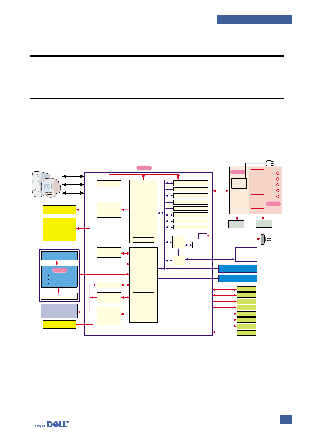
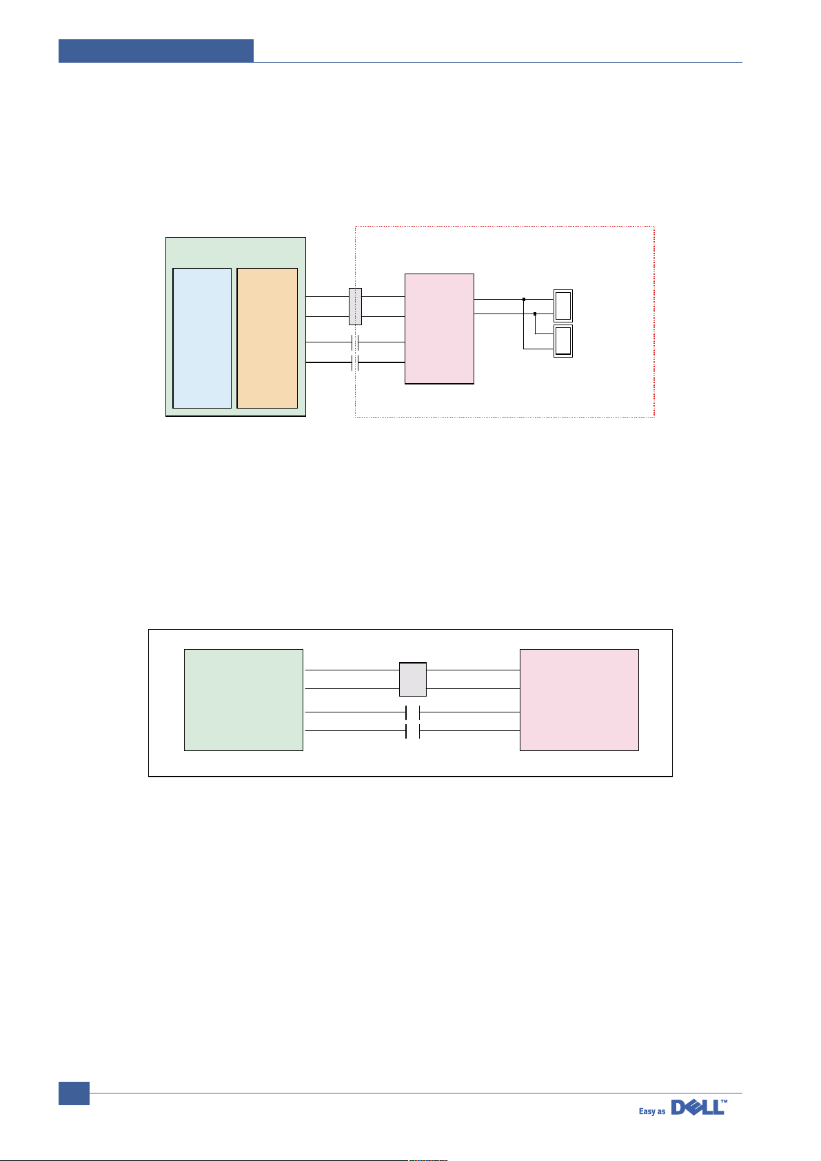
11.1 System Configurations
SCX-4920N is roughly made up Main Control part, Operation Panel part, Scanner part, Line Interface part and
Power part. Each Part is separated Module which focus on common and standard design of different
kind products. main control part adopting Fax & LBP Printer exclusive Controller is composed of 2
CPU and 1 Board. Scanner part is composed of ADF and Platen and is connected with Main by
Harness . Line Interface part is designed to apply TBR21 standard(Domestic, Europe,etc..)
MHV
+5V/
+12V
+24V
+24VS
INLET &
POWER S/W
PAPER EMPTY
SENSOR
EXIT SENSOR
MP EMPTY
SENSOR
FEED SENSOR
COVER S/W
AC PWR
SUPPLY
DEV
THV
OPC GND
SPGPm
ARM946ES
CACHE(16K*2)
SDRAM Control
ROM Control
DMA Control
PVC
GEU/HCT/gCOD
EC
I/O I/F
Engine Control
IEEE1284/USB2.0
MAIN MOTOR
DRIVER
A3977S LR
Reset
THERM
26P
2P
MODEM
SFM336
33.6KBP
AUDIO Drv.
2P
600 DPI, COLOR CCD
MAIN MOTOR
FLATEN MOTOR
FAST SRA M
(128 KB yte)
CIP4
Image P rocesser
AFE I/F
I/O PORT
Motor Control
DMA Control
RTC
JBIG Codec
CIP 4 AFE
FLATEN
MOTOR
DRIVER
TEA3718 X 2EA
CCD DRIVING
PART
USB 2.0
IEEE1284
NETWORK
ADF UNIT
P-REGI, P-DET, P-POS
SENSOR
ADF MOTOR DRIVER
TEA3718 X 2EA
FLAT COVER SENSOR
LCD, 16*2 LINES
14P
3P
FUSER
2P
FAN
2P
NE TWORK INTERFAC E CA RD
SCF (Option)
BootROM
(1MBX2ea or 2MBX2ea)
MEMO RY DIMM
Smart DAA
CX20493
PS3 / PCL6 DIMM(SEC)
SRAM
(128KByte) or
Not Used
SDRAM(16MB or 32MB)
DRAM Backup logic
PCL6(2MB x 2ea)
PS3(2MB x 2 ea) : DELL
3P
LINE
EXT. PHONE
LSU
11P
PTL
DEV_FUSE
MAIN CLUTCH
2P
2P
3P
MP CLUTCH
4P
TONER RX
CARIDGE INFO.
.
TONER TX
4P
3P
4P
AC 110V/220V
MICOM
LCD/LED Drive
Key Scan
OPE
MAIN
SMPS
HVPS
Page 2
Service Manual
Circuit Diagram
11-2
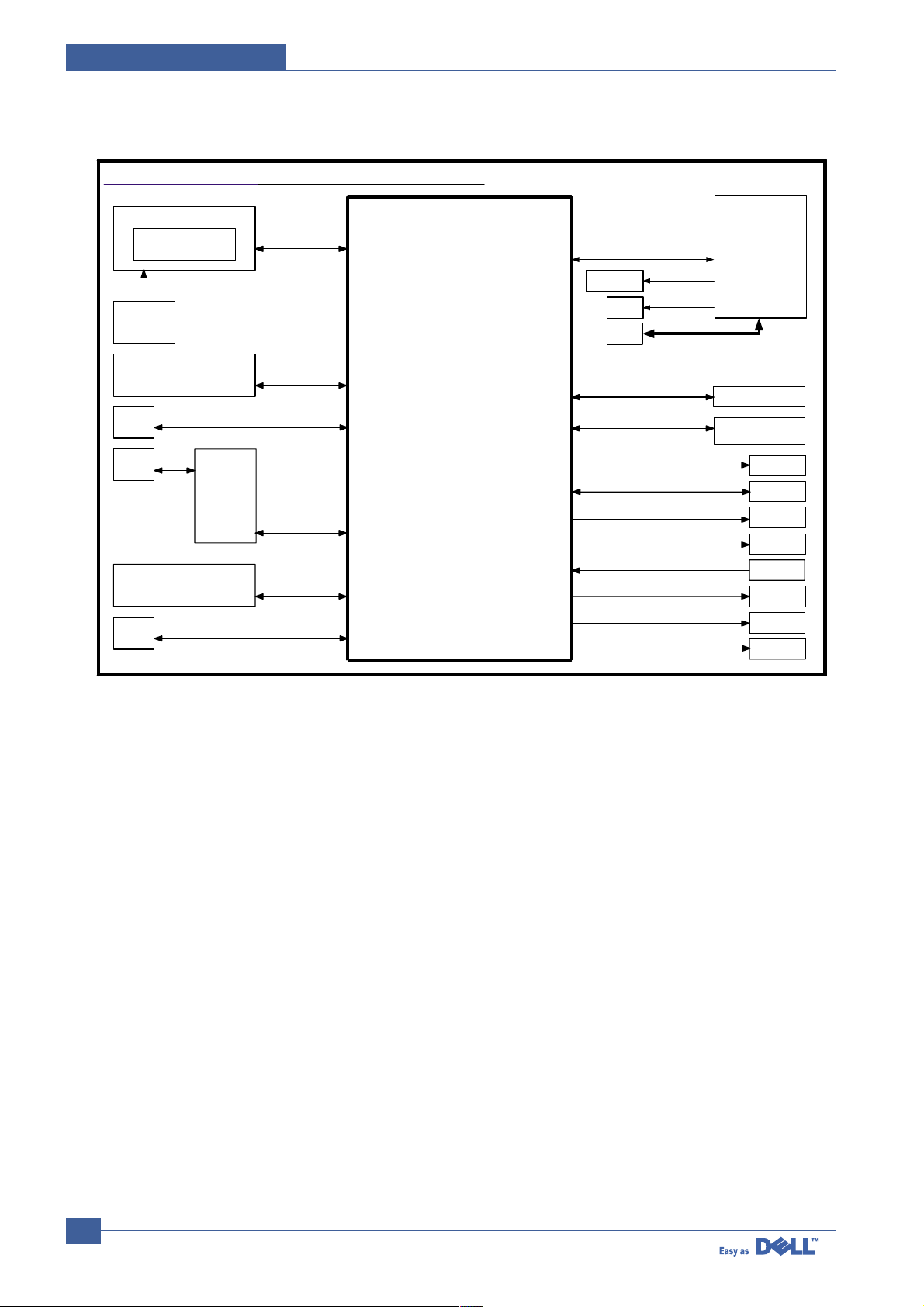
CPU Part
1) CPU : Use 32Bit RISC Processor, ARM946ES,which is exclusive controller to execute Printer & FAX Function
and to execute operation block by flash memory within system program, and to control whole system.
- Main function block
- Completely Integrated System for Embedded Applications,
- 32 Bit Risc Architecture, Efficient and Powerful ARM9 Core.
- LSU Interface Module for Interfacing PVC or HPVC with LSU
- 2 Channel General Purpose DMA Controller for High Speed I/O
- Dual Memory Bus Architecture
- Operation Frequency : AHB Bus: 60MHz, Internal System Bus: 120MHz
- Operation Voltage : 3.3V
- POWER ON RESET TIME :
Laser MFP 1600n CONNECTION DIAGRAM
LCD MODUL E
16 X 2LINE
OPE B’d
1:DGND
2:+5V
3:OPE_TXD
4:OPE_RST
5:OPE_RXD
6 : nLED8
FLATE N
COVER
SENSOR
1:+5V
2:SIGNAL
3:GND
1,3,5,7,8 :DGND
2 : CCD_VOB
4 : CCD_VOR
6 : CCD_VOG
12,16,17,20 : DGND
9,10,11 : CCD_PI_TG
13 : CCD_PI_RS
14 : CCD_PI2
15 : CCD_PI1
16,17,20,24 : DGND
18 : CCD_PI_CP
19 : +5V
21 : CCD_HOME
22 : +24V
23 : INV_POWER
CCD MODULE
FLATEN
MOTOR
1:MA
2:MB
3:MA
4:MB
ADF
MOTOR
DRIVER
SENSOR
-P_POS
-P_PEG
-P_DET
ADF
MOTOR
1:MA
2:MB
3:MA
4:MB
1,4,11,15 : DGND
2:+24V
3:+5V
5:ADF_NA
6:ADF_PHB
7:ADF_PHA
8:ADF_B
9:ADF_NA
10 : ADF_NA
12 : nADF_P_DET
13 : nADF_DET
14 : nADF_P_REG
16 : nADF_P_POS
SCF Unit
1:+3.3V
2 : nS CF_STATUS
3:SCF_CMD
4:SCF_CLK
5:SCF_READY
6:+24V
7,8 : DGND
MAIN
MOTOR
1:MA
2:MB
3:MA
4:MB
1 : P_ EMPT Y
3,4 : +5V
7:+12V
13 : MP_EMPTY
15,22,23 : N.C
17 : N.C
19 : THV_EN
21 : MHV_PWM
25 : FUSER_ON
SMPS / HVPS
MAIN
CLUTCH
MP
CLUTCH
PTL
1:SIGNAL
2:N.C
3:+4VS
1:+24VS
2:SIGNAL
1:+5V
2:SIGNAL
TONER
RX
TONER
TX
CARTRIDGE
1:SIGNAL
2:N.C
3:+24VS
1:+24VS
2:SIGNAL
1:+3.3V
2:CART_DIN
SENSOR
-MPSENSOR
-P_EMPSEN.
-EXITSEN.
- FEED SEN
SWITCH
-DOOROPEN
2:P_FEED
5,6,8,9,10 : GND
11,12 : +24VS
14 : +24V
16 : THV_READ
18 : THV_PWM
20 : DEV_PWM
24 : FAN
26 : P_EXIT
1:LSUCLK
3:nPMOTOR
5:+24VS
7:+5V
LSU
2:nLREADY
4,8,9,11 : DGND
6:nHSYNS
10 : VDO
FAN
PWR
S/W
LIU
LINE / EXT. Phone
1:LINE1
2:LINE2
3:EXT.PHONE
MAIN B’d
SPK
1 : SPK+
2 : SPK-
THERMISTOR
1 : THERMISTER
2 : THERMISTER
FUSER
3 : CART_DOUT
4:DGND
Page 3
Circuit Diagram
Service Manual
11-3
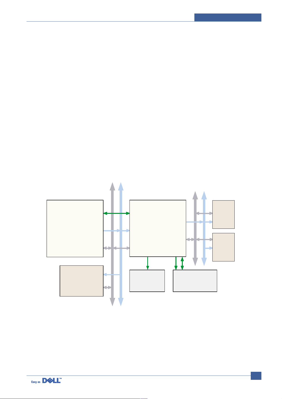
2) Flash Memory : Record System Program, and download System Program by PC INTERFACE.
FAX for Journal List, and Memory for One Touch Dial, Speed Dial List.
- Size : 4M Byte
- Access Time : 70 nsec
3) SDRAM : is used as Swath Buffer in Printing, Scan Buffer in Scanning, ECM Buffer in FAX receiving, and
System Working Memory Area
- size 32MB : 32Mbyte(Basic).
TBD MB :System Working Memory Area and Scan Buffer
TBD MB :FAX Memory Receive Area
TBD MB :Printing System Working Memory Area
- Max Frequency : 133MHz
- store Fax Receive Memory Data by using Battery
MAIN
CONTROLLER
(CPU, DMAC)
SRAM
SRAM
ANALOG
FRONT END
DATA
MEMORY
IMAGE SENSOR
CIP4
data bus address bus
control signals
control signals
data bus address bus
Page 4
Service Manual
Circuit Diagram
11-4
11.2 FAX Section
11.2.1 Modem Part
11.2.1.1 BLOCK DIAGRAM
DSP SSD
System
Side
Dervice
CX20493
LSD
Line
Side
Dervice
Transformer
Capacitor
Ext Line
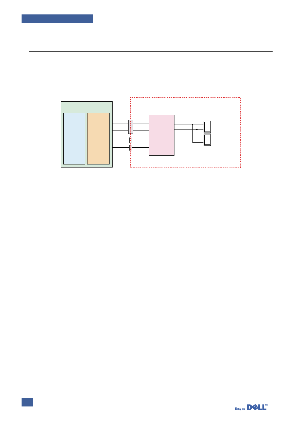
Implemented by based on Conexant DAA (Data Access Arrangement) Solution , and is roughly composed of two
kinds Chip Solution
- CX82500(SFM336) : Existing Modem Chip which adds SSD (System Side Device) for interfacing between -
- LSD and DIB of FM336Plus Core
- CX20493(LSD) : LIU (Line Interface Unit) Chip which is controlled by SSD and satisfies each PSTN
requirements by modulating internal Configuration with connecting Tel Line.
Page 5

Circuit Diagram
Service Manual
11-5
11.2.1.2 Modem(SFM336) specification
• 2-wire half-duplex fax modem modes with send and receive data rates up to 14,400 bps
V.17, V.33, V.29, V.27 ter, and V.21 Channel 2
- Short train option in V.17 and V.27 ter
• PSTN session starting
- V.8 and V.8bis signaling
• HDLC support at all speeds
- Flag generation, 0-bit stuffing, ITU CRC-16 or CRC-32 calculation and generation
- Flag detection, 0-bit deletion, ITU CRC-16 or CRC-32 check sum error detection
- FSK flag pattern detection during high-speed receiving
• Tone modes and features
- Programmable single or dual tone generation
- DTMF receiver
- Tone detection with three programmable tone detectors
• Receive dynamic range:
- 0 dBm to –43 dBm for V.17, V.33, V.29, V.27 ter and V.21 Channel 2
• Programmable transmit level: -9 to –15 dBm
• Serial synchronous data
• Parallel synchronous data
• TTL and CMOS compatible DTE interface
- ITU-T V.24 (EIA/TIA-232-E) (data/control)
- Microprocessor bus (data/configuration/control)
Page 6
Service Manual
Circuit Diagram
11-6
1) Line Interface Signal of Tel Line and LSD is Analog Signal.
2) there is A/D, D/AConverter in LSD, so Analog Signal from Tel Line is transited in Digital through A/D Converter
in DAA and transfer to SSD by DIB Capacitor Digital Signal from SSD is converted to Analog by D/A Converter
in DAA and transfer to Tel Line
3) Transformer transfer Clock from SSD to LSD and Clock Frequency is 4.032MHz. LSD fullwave rectifies Clock to
use as inner Power supply and also use as Main Clock for DIB Protocol Sycn between LSD and SSD.
Transformer transfer Clock by separatin Primary and Secondary, and amplifies Clock Level to LSD by Coil
Turns Ratio 1:1.16.
11.2.1.3 Clock
- Clock is supplied by transformer from SSD to LSD, and There is PWROUT to adjust output impedance of
Clock Out Driver is inside SSD and CLKSHIGH Registor to adjust duty of HLPWR Registor and Clcok. Clock
from SSD to LSD has Differential structure of 180 phase difference for Noise Robustness DIB Data transfer
Data From SSD to LSD By Capacitor, and also transfer specific data from LSD to SSD. after transfering data
to SSD, RSP is transfered and LSD recognize RSP and change LSD to output Driver transfer Data to SSD.
DIB Data form SSD to LSD by Capacitor has Differential structure of 180 phase difference between DIBP and
DIBN for Noise Robustness
Tel Line
CX20493
LSD
Line
Side
Device
CX82500(SFM336)
SSD
System
Side
Device
DSP
Capacitor
Transformer
Primary Parts
Ext Line
LSD
SSD
CLKP
CLKN
DIBP
DIBN
Page 7

Circuit Diagram
Service Manual
11-7
1) Application Network: 3 PSTN (RJ-11)
2) Communication Mode: Half-Duplex, ITU V.8, V.34, V.17, V.29, V.21, ECM
> Modem will auto train down only.
> .
3) Communication Standard: ITU-T Group 3
4) Max. Modem Speed: 33.6 Kbps
5) Encoding: MH, MR, MMR, JPEG
6) Transfer Rate: 3 seconds (standard resolution, MMR, 33.6kbps)
> Phase “C” by ITU-T No.1 Chart/Memory Transmission/ECM
7) Fax Modes: Standard (203 x 98 dpi)
> Fine (203 x 196 dpi)
> Super Fine (300 x 300 dpi)
8) Fax Contrast: Adjustable 3 levels (Light/Normal/Dark)
9) Fax Memory: 4MB (About 300 Sheets of CCITT No.1 Chart at standard resolution).
User selectable parameters will be stored in NVRAM.
10) TX/RX Journal : Available.
1 1) Tel/ID List: Available.
12) Confirmation Reports for Send: Upon successful transmission
> Upon failure
> Reduced image of first page (except OHD, and partial page for
complexity of the images)
> Customer On/Off selectable
13) Management Reports:
> System Data List
> Image TCR for Memory TX
14) TTI/RTI: TTI (Transmit Terminal Identification) printed at top of Fax Image.
> RTI(Receiver Terminal Identification) printed at bottom of Fax
Image the Transmitting devices fax number is substituted for
receving devices fax number is this footer..
15) Line Control Unit (LIU): > Input Sensitivity: Not programmable
> Output Level: 9 to 15 db (programmable)
> Cable Equalization: Not programmable
> Input/Output Impedance: per PTT requirements (programmable)
> DC Resistance: per PTT requirements (programmable)
> Insulation Resistance: Minimum 5M ohm
16) Header Transmission (Always On): Local Machine date and time
> Local Machine ID
> Local Machine Name
> Transmit page count (3 digits)
Page 8

Service Manual
Circuit Diagram
11-8
This is Connection Part between system and PSTN(Public Switched Telephone Network), and 1 st side circuit is
usually located. Main functions are Line Interface, Telephone Connection and Line Condition Monitoring.
1. Telephone Line Connection
• Modular Plug : RJ-11C
• LIU PBA Modular Type : 623 PCB4-4
• Line Code Length : 2m
• Line Code Color : Ivory
11.2.1.4 ON HOOK state Characteristic
1) DC Resistance
• DP Dial Mode (Direct Current 30mA) : 50 ~ 300ohm
• DTMF Dial Mode (Direct Current 20mA) : 50 ~ 540ohm
2) Ring Sensitivity
• Ring detection Voltage : 40Vrms % 150Vrms (condition :Current=25mA,Frequency=15Hz)
product Margin : 30Vrms % 150Vrms
• Ring detection Frequency : 15.3Hz % 68Hz (condition : Voltage=45Vrms,Current=25mA )
product Margin : 15Hz % 70Hz
• Ring detection Current : 20mA % 100mA (condition : Voltage=40Vrms,Frequency=20Hz)
product Margin : over 15mA
3) False Ring Sound
• Ring Frequency : 750Hz + 1020Hz
• Ring interrupt Cycle : On/Off depending on input Ring Signal Cycle.
Page 9

Circuit Diagram
Service Manual
11-9
11.3 Scanner Section
11.3.1 Scan Part
Pictorial signal input part : output signal of CCD passes through Bypass_Cap change to ADC at AFE_CIP4 , and
defined signal between AFE_CIP4 and CIP4 processes the Image signal. When AFE accept each pixel,
CDS(Correlated Double Sampling ) technique which samples arm-level twice is used on each pixel by using CIP4
signal.
1) Pictorial image processing part : read CCD Pixel data in terms of 600dpi Line and process LAT algorithm on
Text mode, Error Diffusion Algorithm on Mixed mode, and store Data at Scan Buffer on PC Scan mode without
algorithm. on every mode Shading Correction and Gamma Correction are executed ahead, then processing is
executed later
* Scan Image Control Specification
• Minimum Scan Line Time : 0.72ms
• Scan Resolution : Max. 600DPI
• Scan Width : 216mm
• main function
- Internal 12bit ADC
- White Shading Correction
- Gamma Correction
- CCD Interface
- 256 Gray Scale
2) CCD Operating Part : CCD Image sensor use +5V and Inverter uses +24V
- CCD Maximum Operating Frequency : 10MHz
- CCD Line time : 0.72ms
- White Data output Voltage : 0.7V & 0.5V (Mono Copy, 0.72ms/line)
- Maximum Inverter Current : 600 mA Max.( +24V)
Page 10

Service Manual
Circuit Diagram
11-10
11.3.2 IP Block Diagram
Crystal
20MHz
CIP4
Oscillation Pad
40MHz
80MHz
SRAM Data
SRAM Address
A/D Converted DataSensor Signal
DMA Request
CPU Address
CPU Data
DMA Acknowledge
Table2
Table1
Table3
Table4
Line
Bufter
CPU
IRQ Ctrl
I/O
Register
Tex DMA
Interface
Sensor
Interface
Image
Engancement
Enlargement/
Reduction
Motor
Control
Vpeak
Control
Gamma
Control
Shading
Acquistion/
Correction
Analog
Front End
Image Sensor
Internal Core
Internal SRAM
External Circuit
Table1: Gamma T able
Table2: IEM T able
Table3: Binary T able
Table4: Motor T able
Extermal
RAM
Control
Binarization
MAIN
MHIMRIMMR
CODEC
Page 11

Circuit Diagram
Service Manual
1) Scanning Device: Color CCD (Charge Coupled Device) Module
2) Supported Operating Systems: Windows 98/2000/NT4.0/ME/XP, MAC (English only, no status
monitor, web download only)
3) Compatibility: TWAIN Standard
4) Maximum Scan Width: 216mm (8.5 inches)
5) Effective Scan Width: 208mm (8.2 inches)
6) Optical Resolution: 600x1200 dpi
7) Interpolated Resolution: Maximum 4800 dpi
8) Preview Scan: 75 dpi
ADF Linearity : 20 sec. (Letter, 300dpi, USB)
Gray Scale : 64 sec. (Letter, 300dpi, USB)
Color : 64 sec. (Letter, 300dpi, USB)
9) Scan Modes/Speeds:
10) ADF Capacity: 50 sheets (20 lb)
11) Image Compression: None
12) PC Interface: > USB (without HUB mode)
Requires 6 ft. USB Cable (not supplied by SEC)
(USB & Parallel are not >
simultaneously supported)
13) Minimum PC Specification: Pentium-II 233MHz, 64MB RAM, 120MB free disk space
14) Registration Position for Original: > Platen: Rear-Left Corner(when facing front/operator panel).
> ADF: Center
15) Number of Copes: 2 digits (99 maximum for LCD display and reports)
11.3.3 Ope Pannel Section
(1)Configuration
operation Panel uses Main Control and separated Ope Chip Micom and work as inner program, systemic
operation is serial system which exchange Date with SIO Port of Main Control. Ope Panel is approximately
composed of Micom part, Matrix part and LCD.
(2) Micom controller
Micom has ROM, RAM, I/O Port built-in and displays and lights LCD by CPU command of Main Control Part
and report Key recognition Data to Main Control Board.
(USB 1.1, 300dpi, Letter
Size, Pentimum 4 1.xGHz,
128MB RAM)
ADF Linearity : 20sec.(Letter, 300dpi, USB)
Gray Scale : 64 sec. (Letter, 300dpi, USB)
Color : 64 sec. (Letter, 300dpi, USB)
Platen Linearity : 18 sec. (Letter, 300dpi, USB)
Gray Scale : 62 sec. (Letter, 300dpi, USB)
Color : 62 sec. (Letter, 300dpi, USB)
11-11
Page 12

Service Manual
Circuit Diagram
11-12
11.4 Printer Section
Printer is consisted of the Engine parts and F/W, and said engine parts is consisted of the mechanical parts
comprising Frame, Feeding, Developing, Driving, Transferring, Fusing, Cabinet and H/W comprising the main
control board, power board, operation panel, PC Interface.
The main controller is consisted of Asic(SPGPm) parts, Memory parts, Engine interface parts and it functions as
Bus Control, I/O Handing, drivers & PC Interface by CPU.
Memory Access supports 16bit Operation, and Program Memory 2MB and Working Memory as well.
The Engine Board and the Controller Board are in one united board, and it is consisted of CPU part and print part
in functional aspect. The CPU is functioned as the bus control, I/O handling, drivers, and PC interface. The main
board sends the Current Image, Video data to the LSU and manages the conduct of Electrophotography for
printing. It is consisted of the circuits of the motor (paper feed, pass) driving, clutch driving, pre-transfer lamp
driving, current driving, and fan driving. The signals from the paper feed jam sensor and paper empty sensor are
directly inputted to the main board.
1) Printing Method: Laser-based Electrophotography
2) Supported Operating Systems: Windows 98/2000/NT4.0/ME/XP/ MAC (English only, no status
monitor, web download only)
3) Emulation: SPL(GDI) , PCL6, PS3,PCL5e
4) Maximum Paper Size: Legal
5) Effective Printing Width: > Letter/Legal: 208mm
> A4: 202mm
6) Resolution: > Addressable 1200 x1200 dpi
(selectable from Print Driver) > 600x600 dpi (True; no RET)
7) Speed: 22ppm (Letter)
8) Input Paper Capacity: > Tray: 250 sheets (20 lb)
> Bypass: Single sheet
9) Output Paper Capacity: 150 sheets (20 lb; sequenced 1 to N, face down)
10) Feed Direction: Front In, Front Out (FIFO)
11) PC Interface: > USB 2.0(without HUB mode)
Requires 6 ft. USB Cable (not supplied by SEC)
12) Toner Cartridge: > Toner Low Sensor: None
> Toner Low Indicator: Message displayed on LCD
> Cartridge Missing Indicator: Message displayed on LCD
13) Paper Sensing: > Tray: “Add Paper” message displayed on LCD
> Bypass: “Add Paper” message displayed on LCD
Page 13

Circuit Diagram
Service Manual
11-13
11.4.1 ASIC
• ARM946ES
- 32-bit RISC embedded processor core
- 16KB instruction cache and 16KB data cache
- No Tightly Coupled Memory
- Memory Protection Unit & CP15 control program
• Dual bus architecture for bus traffic distribution
- AMBAHigh performance Bus (AHB)
- System Bus with SDRAM
• Printer Video Controller for LBP engines
• Graphic Execution Unit for banding support of Printer Languages
• Printer Video Controller for LBP engines
- PVC : Printer Video Controller without RETAlgorithm
- HPVC : Printer Video Controller with RET algorithm
(Line Memory & Lookup Table Memory : 512 x 8 , 4096 x 16)
• Engine Controller
- Motor Control Unit
- Motor Speed Lookup Table Memory (128 x 16 x 2)
- Pulse Width Modulation Unit
- 4 Channels are supported
- ADC Interface Unit
- 3 ADC Channels are available
- ADC Core (ADC8MUX8) maximum clock frequency : 3 MHz
• USB 2.0 Interface
• Package : 272 pins PBGA
• Power : 1.8V(Core), 3.3V(IO) power operation
Page 14

Service Manual
Circuit Diagram
11-14
11.4.2 Speed : 166MHz core(ARM946ES) operation, 60MHz bus operation
ADDR/
DATA
MUX
ROM
CONTROLLER
EXTERNAL
DMA CONTROLLER
(4CH)
ARM946E-S CORE
16KB ICACHE
16KB DCACHE
USB2.0
ARBITER
DECODER
MAC
SYSMAC
SFR Bus
AHB Bus
System Bus
SYSTEM BUS
ARBITER
SYSTEM PLL
(120MHz)
CLOCK & RESET
GENERAT OR
SDRAM
CONTROLLER
(5CH)
GRAPHIC
EXECUTION
UNIT
ROTATOR/
SCALER/
HALFTONER
1024x8, 256x8x4
EPI
MISC
CONTROLLER
PARALLEL PORT
INTERFACE
HCT
ENGINE
CONTROLLER
UART(3CH)
gCODEC
TIME CONTROL
UNIT
INTERRUPT
CTRL (5CH)
ENGINE
Comm. I/F
ADC (3CH)
MOTOR
CONTROLLER
128x16x2
PULSE WIDTH
MODULATOR
HPVC
512x8
4096x16
PVC
LSU I/F
SFR BUS
INTERFACE
IO
CONTROLLER
SYSTEM
BUS
INTERFACE
Page 15

Circuit Diagram
Service Manual
11-15
11.5 Copier Section
1) Copy Mode: Black and White
2) Scanner Type: CCD with Flatbed/Platen and ADF
3) Maximum Size of Original: > Platen: 216 x 297 mm
> ADF: Legal (216 x 356 mm)
(max. width = 218 mm,
max length = 400 mm)
4) Optical Resolution: 600 x 600 dpi
5) Copy Quality - H x V: > Text : 600 x 300 dpi (default)
(User selectable via Content button) > Mixed : 600 x 300 dpi
> Photo : 600 x 600 dpi
6) Supported Media Types: Plain, Label, Cardstock, Transparency
7) Copy Speed: > Platen, SDMP: 22cpm (Letter)
(SDMP = Single Document, > ADF, SDMP: 22cpm (Letter)
Multiple Printout, > ADF, MDSP: 7cpm (Letter, Text or Mixed)
4cpm (Letter, Photo)
MDSP = Multiple Document,
Single Printout)
8) Reduce/Enlarge: Platen: 25% - 400% (1% increments)
> ADF: 25% - 100% (1% increments)
9) Non-printable Area: 4 mm (Top, Bottom, and each Side)
10) Copy Count: 1 to 99
(Page count displayed on LCD
during copy operation)
11) Copy Modes: Text, Mixed, Photo
12) Fixed R/E Setting: 1 00%, Auto-fit, 2(4)-Up
13) Darkness Control: 3 levels
14) First Copy Output Time (FCOT): > Platen: 10 sec. (600 x 300 dpi)
> ADF: 15 sec. (600 x 300 dpi)
15) Duplex Copy > TBD
Page 16

Service Manual
Circuit Diagram
11-16
11.6 Telephone Section
1) Speed Dial: 200 Locations (46 digits maximum per location)
2) On-hook Dial (manual fax): Yes
3) Last Number Redial: Yes
4) Automatic Redial: Y es
5) Pause: Yes (using Redial key)
6) Ringer Volume: Off, Low, Medium, High
7) Tone/Pulse: Selectable (Tech Mode Only no Telecom certification for Pulse mode)
11.7 SMPS & HVPS Section
The SMPS supplies DC Power to the System.
It takes 110V/220V and outputs the +5V, +24V to supply the power to the main board and ADF board. The HVPS
board creates the high voltage of THV/MHV/Supply/Dev and supplies it to the developer part for making best
condition to display the image. The HVPS part takes the 24V and outputs the high voltage for THV/MHV/BIAS,
and the outputted high voltage is supplied to the toner, OPC cartridge, and transfer roller.
11.7.1 HVPS (High Voltage Power Supply)
• Transfer High Voltage (THV+)
> Input Voltage : 24 V DC & 15%
> Output Voltage : MAX +5.0KV & 5 %,(Duty Variable, no loading )
- 1.2KV & 15% (when cleaning,200 ( )
> Output Voltage Trigger : 6.5 )
> Input contrast of the Voltage stability degree :under & 5 % (fluctuating input 21.6V % 26.4V)
Loading contrast : & 5 % or less
> Output Voltage Rising Time : 100 ms Max
> Output Voltage Falling Time : 100 ms Max
> Fluctuating transfer voltage with environmental various : +650 V(Duty 10%) ~ 5 KV (Duty 90%)
> Environment Recognition Control Method : The THV-PWM ACTIVE is transfer active signal. It detects the
resistance by recognizing the voltage value, F/B, while permits the environmental recognition voltage.
> Output Voltage Control Method : Transfer Output Voltage is outputted and controlled by changing Duty of
THVPWM Signal. 10% Duty : +650V, 90% Duty : +5KV & 5%
Page 17

Circuit Diagram
Service Manual
11-17
• Charge Voltage (MHV)
> Input Voltage : 24 V DC & 15%
> Output Voltage : -1.3KV ~ -1.8KV DC +/- 50V
> Output Voltage Rising Time : 50 ms Max
> Output Voltage Falling Time : 50 ms Max
> Output Loading range : 30 M * ~ 1000 M *
> Output Control Signal(MHV-PWM) : CPU is HV output when PWM is Low
• Cleaning Voltage (THV-)
> The (+) Transfer Voltage is not outputted because the THV PWM is controlled with high.
> The (-) Transfer Voltage is outputted because the THV-Enable Signal is controlled with low
> The output fluctuation range is big because there is no Feedback control.
• Developing Voltage (DEV)
> Input Voltage : 24 V DC & 15%
> Output Voltage: -200V ~ -600V DC & 20 V
> Output Voltage Fluctuation range: PWM Control
> Input contrast of the output stability degree : & 5 % or less
Loading contrast : & 5 % or less
> Output Voltage Rising Time : 50 ms Max
> Output Voltage Falling Time : 50 ms Max
> Output Loading range : 10M * ~ 1000 M *
> Output Control Signal (BIAS-PWM) : the CPU output is HV output when PWM is low.
•S upply
> Output Voltage : -400 V ~ -800V DC & 50 V(ZENER using, DEV )
> Input contrast of the output stability degree : under & 5 %
Loading contrast : & 5 % or less
> Output Voltage Rising Time : 50 ms Max
> Output Voltage Falling Time : 50 ms Max
> Output Loading range : 10 M * ~ 1000 M *
> Output Control Signal (BIAS-PWM) : the CPU is HV output when PWM is low.
Page 18

Service Manual
Circuit Diagram
11-18
11.7.2 SMPS (Switching Mode Power Supply)
It is the power source of entire system. It is assembled by an independent module, so it is possible to use for
common use. It is mounted at the bottom of the set.
It is consisted of the SMPS part, which supplies the DC power for driving the system, and the AC heater control
part, which supplies the power to fuser. SMPS has two output channels. Which are +5V and +24V.
• AC Input
> Input Rated Voltage : AC 220V ~ 240V AC 120V / AC 220V(EXP version)
> Input Voltage fluctuating range : AC 198V ~ 264V AC 90V ~ 135V / AC 198V ~ 264V
> Rated Frequency : 50/60 Hz
> Frequency Fluctuating range : 47 ~ 63 Hz
> Input Current : Under 5.0Arms / 2.5Arms (But, the status when lamp is off or rated voltage is
inputted/outputted )
• Rated Output Power
NO ITEM CH2 CH3 Remark
1 CHANNEL NAME +5V +24.0V
2 CONNECTOR PIN CON 3 CON 3
5V PIN: 8 24V PIN:11,12,13
GND PIN: 7 GND PIN:9,10
3 Rated Output +5V & 5% +24V & 10%
(4.75 % 5.25V) (21.6 % 26.4V)
4 Max. Output voltage 0.14 A 2.0 A
5 Peak Loading voltage 0.14 A 2.5 A 1ms
6 RIPPLE NOISE 100mVp-p Under 500mVp-p
Voltage
7 Maximum output 0.35W 48W
8 Peak output 0.7W 60W 1ms
9 Protection for loading -
shortage and
overflowing current
Page 19

Circuit Diagram
Service Manual
11-19
• Consumption Power
• Length of Power Cord : 1830 & 50mm
• Power Switch : Use
• Feature
> Insulating Resistance : 50 ( or more (at DC 500V)
> Insulating revisiting pressure : Must be no problem within 1 min. (at 1500Vac,10mA)
> Leaking Current : under 3.5mA
> Running Current : under 40A PEAK (AT 25 + , COLD START)
under 60A PEAK (In other conditions)
> Rising Time : within 2Sec
> Falling Time : over 20ms
> Surge : Ring Wave 6KV-500A (Normal, Common)
• Environment Condition
> Operating temperature range : 0 +% 40 +
> Maintaining temperature range : -25 +% 85 +
> Preserving Humidity Condition : 30% % 90% RH
> Operating atmospheric pressure range : 1atm
• EMI Requirement : CISPR ,FCC, CE, MIC, C-Tick.
• Safety Requrement :IEC950 UL1950, CSA950, C-UL,NOM,TUV,Semko,Nemko,iK,CB, CCC(CCIB),GOST,
EPA, Power Save
NO ITEM CH2 (+5V) CH3 (+24V) Remark
1 Stand-By 0.07A 0.4 A AVG:55 Wh
2 PRINTING 0.14A 2.0 A AVG 350 Wh
3 Sleep-Mode 0.01A 0.4A AVG : 20 Wh
Page 20

Service Manual
Circuit Diagram
11-20
11.7.3 Fuser Ac Power Control
Fuser(HEAT LAMP) gets heat from AC power. The AV power controls the switch with the Triac, a semiconductor
switch. The ‘ON/OFF control’is operated when the gate of the Triac is turned on/off by Phototriac (insulting part).
In other words, the AC control part is passive circuit, so it turns the heater on/off with taking signal from engine
control part.
When the ‘HEATER ON’ signal is turned on at engine, the LED of PC1 (Photo Triac) takes the voltage and
flashes. From the flashing light, the Triac part (light receiving part) takes the voltage, and the voltage is supplied to
the gate of Triac and flows into the Triac. As a result, the AC current flows in the heat lamp, and heat is occurred.
On the other hand, when the signal is off, the PC1 is off, the voltage is cut off at the gate of Triac, the Triac
becomes off, and then the heat lamp is turned off.
• Triac (THY1) feature :12A, 600V SWITCHING
• Phototriac Coupler (PC3)
> Turn On If Current : 15mA% 50mA(Design: 16mA)
> High Repetive Peak Off State Voltage : Min 600V
 Loading...