

Repair Manual
Repair Manual
1. Block Diagram
2. Connection Diagram
3. Circuit Description
4. Schematic Diagrams
CONTENTS
INKJET PRINTER(MFP)
SCX-1150F
1
1-1
Samsung Electronics
BLOCK DIAGRAM
Repair Manual
1. Block Diag ram
AC
( 110~240
(64Mbit)
V)
SMPS
( 30V, 3. 3V)
Jupi t er3
UART 3
I/OPORT
INT. CNTR
USB
FLASH
Thunder bol
t
MOTOR
CCD Module
SCA NSTEPPER
SCAN MOTOR
(UNI-POLAR STEP)
COLOR
MON O
C A RTR I DG E
RESET
USB
PC
10MHz
48MH z
P1284 CONN
SCANNER
BU F FE
600/ / 600
Tx/ Rx
SPEAKER
SDRAM
AFE
BACK UP
(Super cap 1F)
ADF MODULE
ADF
RTC
Cl o c k
SDRA M
MODEM
Spi t f i r e
/REQ /ACK
ADC
DOC. POS SENSOR
DOC. DET SENSOR
OPE
POWER
+5V
+11.75V
+30V
+3.3V
LIUMAIN
PRINT HEAD(2PEN)
600DPI DOUBLE
HEIGHT
ENCORDER
SENSOR
LINE FEED
CARRIAGE
RETURN MOTOR
COVER OPEN SENSOR
PAPER
EXIT
SENSOR
IMAGE
PROCESSOR
OA-980
IEEE 1284
TIMERS
REAL TIME CLOCK
ARM7TDMI
MEM. SNTR
Head Control I/F
SCAN SNTR
DERASTERIZER
MODEM CLOCK
28.224MHz
MAIN CLOCK
ADF STEPPER
MOTOR DRIVER
KEY PANNEL
TELEPHONE
LINE
MODEM & EXT_PHONE
SEPERATING PART
EXTERNAL
LINE
RING
DETECTION
PA RT
EXTERNAL
PHONE
DETECTION
PA RT
TRANSFORMER
(64Mbit)
(8Mbit)
(33.6Kbps)

2
2-1
Samsung Electronics
CONNECTION DIAGRAM
Repair Manual
2. Connection Dia gr am
Refer to the Schematic diagram(See page 4-2)
3
3-1
Samsung Electronics
CIRCUIT DESCRIPTION
Repair Manual
3. Circuit Description
3-1. GENERAL DESCRIPTION
Main circuit consists of mainly consists of CPU and the controller part with various types of built-in I/O device driver(built-in
RISC Processor Core: ARM7TDMI), system memory part, OA980 controlling input of image received from media and con version, CF(COMP ACTstorage card) interface part. The following nomenclatures by section is the same as those listed in
the circuit diagram.
3-2. MEMORY MAP
The entire Addressing area provided by MAIN CONTROLLER(S3C46MOX(Jupiter3)) is 256MBytes from 0x00000000 to
0x10000000, and the Max. Address Range for each External Chip Select is 32M Byte or Half word from 0x000000 to
0x01FFFFFF and embodied with Big-Endian Bus interface. MEMORY area is divided into EXTERNAL ROM and RAM
areas(See (Figure 1)), and the areas actually used are 8M/8M BYTES SDRAM and 1M BYTES ROM(FLASH MEMORY).
0x0FFF_FFFF
GCS 7 Area
0x0E00_0000
0x0DFF_FFFF
GCS6 Area - DRAM(8MB)
0x0C00_0000
0x0BFF_FFFF
Reserved
0x0A00_0000
0x09FF_FFFF
GCS 4 Area - OA980 PO CS
0x0800_0 000
0x07FF_FFFF
GCS 3 Area - EXTENDED GPIO
0x0600_0 000
0x05FF_FFFF
GCS 2 Ar ea - MODEM
0x0400_0 000
0x03FF_FFFF
GCS 1 Area - OA980
0x0200_0 000
0x01FF_FFFF
Special Registers
0x01C0_0000
0x000F_FFFF
Program Area(1MB
used)
0x0000_0 000
USER MEMORY(3MB Start ~ )
0xC300000
PIXEL TO LINE BUFFER(30KB)
0xC2CBC20
Chunk Bu ffer(8KByte)
0xC2 C9C20
Re ad P rint B uffe r ( 32B yte)
0xC2 C9C00
Swath Buffer(300KByte)
0xC27EC00
Scan Buffer(810KB)
0xC1B4400
RGB Buffer(30KB)
0xC1ACC00
ECM Buffer(64KB)
0xC1 9C C00
RCP PC FAX Buffer(15KB)
0xC199000
JPEG DECODE BUFFER(64KB)
0xC099000
MDM Out Buffer(20KB)
0xC094000
MDM In Buffer(28KB)
0x C08D 000
JPEG INPUT Buffer(220KB)
0xC056000
System AREA(344K)
0xC000000
OASIS Rom Code : 256KB
(Sector 15 ~ Sector 18)
J3 ROM Code :704KB
(Sector 4 ~ Sector 14)
Backup Data(Sector 3:32KB)
Not Used(Sector 1,2: 16 KB)
Boot Rom Code(Sector 0 : 16KB)
Flash memory(1MB)
SDRAM(8MB)
<Figure 1. S3C46MOX(Jupiter3) MEMORY MAP>
◊ MAIN PBA

3-2
CIRCUIT DESCRIPTION
Samsung Electronics
Repair Manual
3-3.DETAILED DESCRIPTION
3-3-1 BLOCK DIAGRAM and MAIN CONTROLLER description
3-3-1-1 General description
MAIN CONTROLLER(S3C46MOX(Jupiter3),U15) consists of this system consists of CPU(ARM7TDMI RISC PROCESSOR), 8K BYTES CACHE, DATAand ADDRESS BUS, PLL deriding input frequency and CLOCK CONTROL part,
SERIAL COMMUNICATION part supporting UART, PRINT HEAD control part, PARALLELPORTINTERFACE part,
USB INTERFACE part, External DMApart for receiving data from external COLOR IMAGE PROCESSOR(OA980,U21), MEMORY and EXTERNAL BANK control part, SYNCHRONOUS SERIAL INTERFACE control part for interfacing Thunderbolt, and LF/CR Motor drive control and general purpose I/O control parts.(See Figure 2 )
3-3-2 S3C46MOX(Jupiter3) FUNCTION DESCRIPTION
3-3-2-1 SYSTEM CLOCK
There are two ways of Clock input method. One is the method to make Master Clock(MCLK) at the internal PLLby connecting X-tal and Capacitor to the outside, and another method is to use MCLK(When inputting 40MHz) directly, which
supplies maximum 40MHz Clock to the EXTCLK terminal(PIN65). The range of frequency being input in case of using
X-tal is limited to 4MHz~10MHz. This system uses SSCG(FS781) with a 10MHZ X-tal outside to make MCLK, and supplies Clock to the XIN terminal(PIN67) of ASIC by expanding Spectrum with bandwidth about 1.5% in comparison with
the basic frequency by using this IC. Inside the ASIC, the PLL makes 66MHz MCLK signal, which is the basic operation
frequency of the System. Also, this PLLmakes 48MHz, the operation frequency of USB Controller.
3-3-2-2 DATA and ADDRESS BUS CONTROL
1. /RD & /WR
/RD & /WR SIGNAL are synchronized with the inside MCLK(66MHZ) and becomes active to Low.
These signal are Strobe Signal used to Read or Write data when each Chip Select becomes active connected to
/RD,/WR PIN of RAM, ROM, OA-980.
2. CHIP SELECT (/ROMCS, /IP_CS,/MED_CS,/SCS0,/SCS1)
- /ROMCS : FLASH MEMORY(U7) CHIP SELECT (LOW ACTIVE)
- /IP_CS : OA-980(U21) CHIP SELECT
(LOW ACTIVE)
- /SCS1 : SDRAM(OPTION)(U12) CHIP SELECT (LOW ACTIVE)
In case each Chip Select is low, it may Read or Write data.
3. D0 ~ D15
- 16BIT DATA BUS
4. A0 ~ A24
- ADDRESS BUS (A23 ~ A24 RESERVED)
3-3
Samsung Electronics
CIRCUIT DESCRIPTION
Repair Manual
<Figure 2. Block Diagram of Main Part>
AC
( 110~240
(64Mbit)
V)
SMPS
( 30V, 3. 3V)
Jupi t er3
UART 3
I/OPORT
INT. CNTR
USB
FLASH
Thunder bol
t
MOTOR
CCD Module
SCA NSTEPPER
SCAN MOTOR
(UNI-POLAR STEP)
COLOR
MON O
CARTRI DGE
RESET
USB
PC
10M Hz
48MH z
P1284 CONN
SCANNER
BU F FE
600/ / 600
Tx/ Rx
SPE AKER
SDRAM
AFE
BACK U P
(Super cap 1F)
ADF MODULE
ADF
RTC
Cl o c k
SDRA M
MODEM
Spi t f i r e
/REQ /ACK
ADC
DOC. POS SENSOR
DOC. DET SENSOR
OPE
POWER
+5V
+11.75V
+30V
+3.3V
LIUMAIN
PRINT HEAD(2PEN)
600DPI DOUBLE
HEIGHT
ENCORDER
SENSOR
LINE FEED
CARRIAGE
RETURN MOTOR
COVER OPEN SENSOR
PAPER
EXIT
SENSOR
IMAGE
PROCESSOR
OA-980
IEEE 1284
TIMERS
REAL TIME CLOCK
ARM7TDMI
MEM. SNTR
Head Control I/F
SCAN SNTR
DERASTERIZER
MODEM CLOCK
28.224MHz
MAIN CLOCK
ADF STEPPER
MOTOR DRIVER
KEY PANNEL
TELEPHONE
LINE
MODEM & EXT_PHONE
SEPERATING PART
EXTERNAL
LINE
RING
DETECTION
PA RT
EXTERNAL
PHONE
DETECTION
PA RT
TRANSFORMER
(64Mbit)
(8Mbit)
(33.6Kbps)
3-4
CIRCUIT DESCRIPTION
Samsung Electronics
Repair Manual
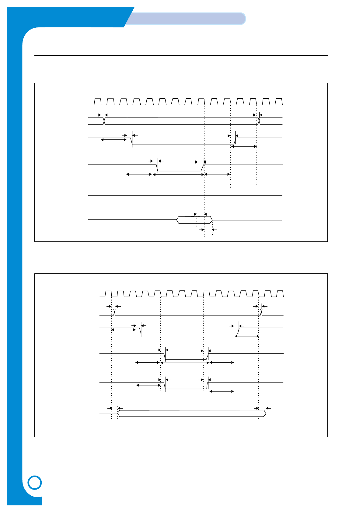
<Figure 3. Flash Memory Read Timing>
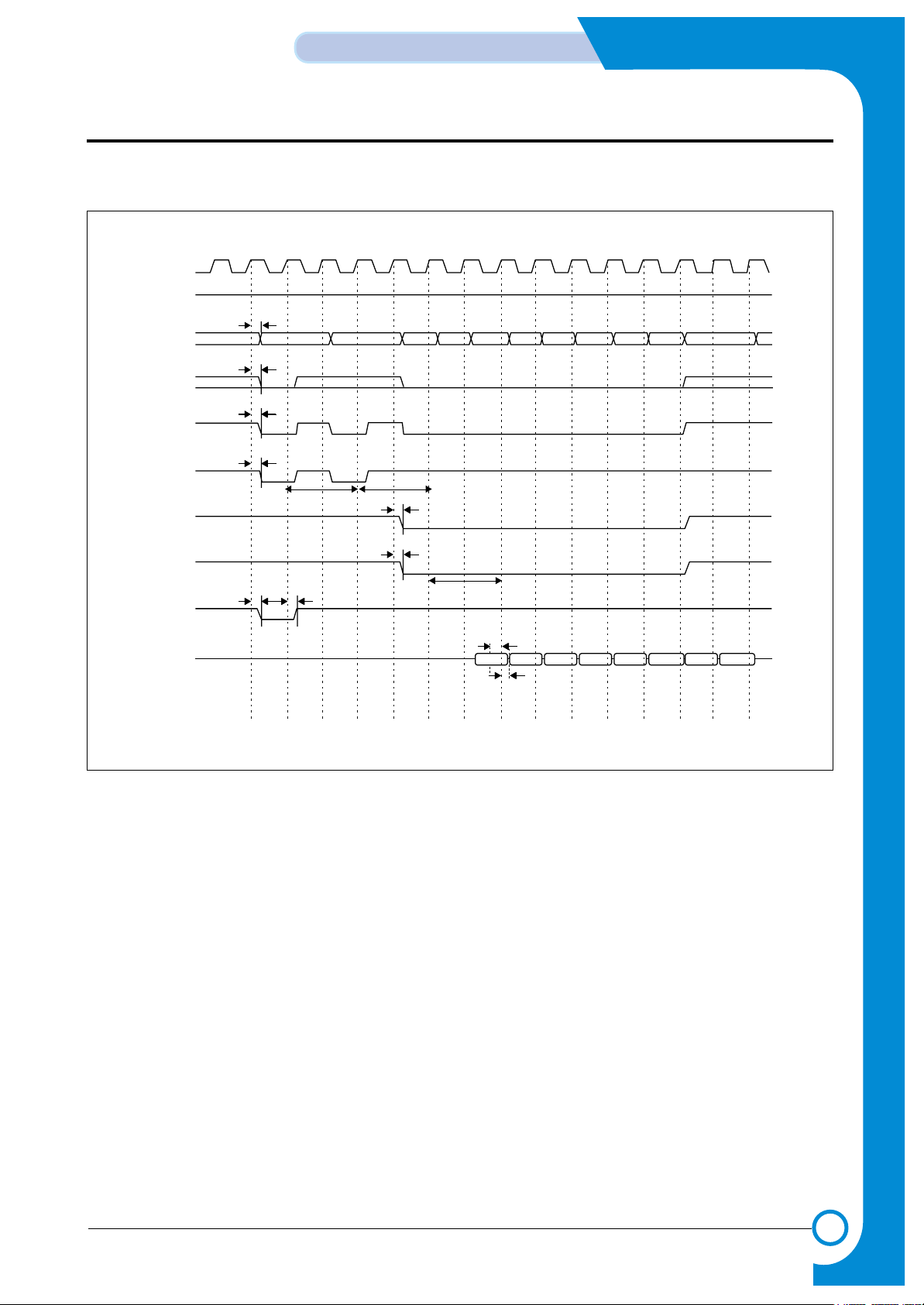
<Figure 4. Flash Memory Write Timing>
EXTCLK
nGCSx
nGCSx
ADDR
tRWD
tRAD
Tacs
tRCD
nWE
DATA
nBEx
Tacc
Toch
Tcah
Tocs
tRCD
tRWD
tRDD
tRAD
tRDH
’1’
EXTCLK
ADDR
nGCSx
nWE
nGCSx
nBEx
DATA
tRAD
tRCD
Tacs
tRWD
Tocs
tRWBED
Tcos
tRDD
Tacc
tRAD
tRCD
Tcah
tRWD
Toch
tRWBED
Toch
tRDD
3-5
Samsung Electronics
CIRCUIT DESCRIPTION
Repair Manual
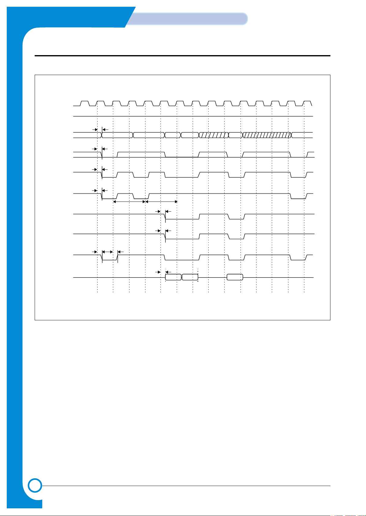
<Figure 5. SDRAM Read Timing>
SCLK
SCKE
ADDR/BA
AP/A10
nGCSx
nSRAS
nSCAS
nBEx
nWE
DATA
’1’
tSAD
tSAD
tSCSD
tSRD
Trp Trcd
tSCD
tSBED
Tcl
tSWD
tSDS
tSDH
3-6
CIRCUIT DESCRIPTION
Samsung Electronics
Repair Manual
<Figure 6. SDRAM Write Timing>
SCLK
’1’
SCKE
ADDR/BA
AP/A10
nGCSx
nSRAS
nSCAS
nBEx
nWE
DATA
tSAD
tSAD
tSCSD
tSRD
Trp
Trcd
tSWD
tSDD
tSDD
tSBED
tSCD
3-7
Samsung Electronics
CIRCUIT DESCRIPTION
Repair Manual
<Figure 7. SDRAM Write Timing>
SCLK
SCKE
ADDR/BA
AP/A10
nGCSx
nSRAS
nSCAS
nBEx
nWE
DATA
tSAD
’1’
’1’
’HZ’
tSAD
tSCSD
tSRD tSRD
tSCD
tSWD
tSCSD
tSAD
Trp Trc
3-8
CIRCUIT DESCRIPTION
Samsung Electronics
Repair Manual
<Figure 8. SDRAM auto Refresh Timing>
SCLK
SCKE
ADDR/BA
AP/A10
nGCSx
nSRAS
nSCAS
nBEx
nWE
DATA
tSAD
’1’
’1’
’HZ’
tSAD
tSCSD
tSRD tSRD
tSCD
tSWD
tSCSD
tSAD
Trp Trc
3-9
Samsung Electronics
CIRCUIT DESCRIPTION
Repair Manual
<Figure 9. SDRAM Self Refresh Timing>
SCLK
SCKE
ADDR/BA
AP/A10
nGCSx
nSRAS
nSCAS
nBEx
nWE
DATA
’HZ’
tSWD
’HZ’
’1’
’1’
’1’
’1’
’1’
’1’
’1’
tCKED
tSAD
tSAD
tSCSD
tSRD tSRD
tSCD
tSCSD
tSAD
tCKED
Trc
Trp
3-10
CIRCUIT DESCRIPTION
Samsung Electronics
Repair Manual
Parameter Symbol Min T yp. Max Unit
ROM/SRAM Address Delay
t
RAD - 12 - ns
ROM/SRAM Chip select Delay
t
RCD - 11 - ns
ROM/SRAM Output enable Delay
t
ROD - 1 1 - ns
ROM/SRAM read Data Setup time
t
RDS - 1 - ns
ROM/SRAM read Data Hold time
t
RDH - 5 - ns
ROM/SRAM Byte Enable Dalay
t
RBED - 13 - ns
ROM/SRAM Write Byte Enable Delay
t
RWBED - 14 - ns
ROM/SRAM output Data Delay
t
RDD - 14 - ns
ROM/SRAM external Wait Setup time
t
WS - 1 - ns
ROM/SRAM external Wait Hold time
t
WH - 5 - ns
ROM/SRAM Write enable Delay
t
RWD - 14 - ns
DRAM Address Delay
t
DAD - 12 - ns
DRAM Row active Delay
t
DRD - 11 - ns
DRAM Read Column active Delay
t
DRCD - 1 1 - ns
DRAM Output enable Delay
t
DOD - 12 - ns
DRAM read Data Setup time
t
DDS - 1 - ns
DRAM read Data Hold time
t
DDH - 5 - ns
DRAM Write Cas active Delay
t
DWCD - 14 - ns
DRAM Cbr Cas active Delay
t
DCCD - 12 - ns
DRAM Write enable Delay
t
DWD - 13 - ns
DRAM output Data Delay
t
DDD - 14 - ns
SDRAM Address Delay
t
SAD - 4 - ns
SDRAM Chip Select Delay
t
SCSD - 4 - ns
SDRAM Row active Delay
t
SRD - 4 - ns
SDRAM Column active Delay
t
SCD - 4 - ns
SDRAM Byte Enable Delay
t
SBED - 5 - ns
SDRAM Write enable Delay
t
SWD - 5 - ns
SDRAM read Data Setup time
t
SDS - 4 - ns
SDRAM read Data Hold time
t
SDH - 0 - ns
SDRAM output Data Delay
t
SDD - 8 - ns
SDRAM Clock Enable Delay
t
CKED - 5 - ns
< ROM/SRAM Bus Timing Constants >
(V
DDP
: 3.3V, V
DDI
: 2.5V, Ta =25˚C, PLCAP=70pf, Max/Min=typ. ±30%)

3-11
Samsung Electronics
CIRCUIT DESCRIPTION
Repair Manual
3-3-2-3 EXTERNAL DMA part
The function of this part is to bring data from external
DEVICE(OASIS:U21) by using GENERAL DMA. If DMA
REQUEST(/IP_REQ) is sent from external DEVICE to
S3C46MOX(JUPITER3:U15), DMA ACKNOWLEDGE
SIGNAL(/IP_ACK) is activated and the GENERAL DMA is
driven, so READ STROBE(/RD) in the external DEVICE to
bring data from the external DEVICE requiring CHANNEL.
To transfer this DA TA to the DESTINATION MEMORY, the
ADDRESS of the DESTINATION MEMORY, CHIP
SELECT and WRITE STROBE(/WR) are generated to
store.
That is, if the EXTERNAL DMA is required by the external
DEVICE, S3C46MOX(Jupiter3:U15) responds to drive the
inside DMA CONTROLLER and then allocate GENERAL
DMA to external CHANNEL so that the data may be transferred to MEMORY TO MEMORY or external DEVICE TO
MEMORY.
• For more details, see the circuit description, see the circuit
description part of IMAGE PROCESSOR (5.3).
3-3-2-4 DRAM control part
Since S3C46MOX(Jupiter3) has the DRAM CONTROLLER build-in, it may be used by connecting DRAM
with external memory.
The Control mode of DRAM CONTROLLER provided by
S3C46MOX(Jupiter3) is available for EARLY WRITE,
NORMAL READ, PAGE MODE, and BYTE/HALF WORD
ACCESS, and is supported even by EDO DRAM,and
SDRAM as well as, Fast page DRAM.
This system uses SDRAM, and the signal used for
READ/WRITE uses /RD,/WR signal used for SYSTEM
BUS CONTROL. It is supported with auto REFRESH and
also by the Self-refresh mode for DRAM
BACK UP. It con-
sists of 2 Banks connected to co
mmon /SCS[1:0], /SCAS,
/SRAS, /SCLK, /SCKE, /DQM[1:0], each of them may use
up to 2M ~ 32M HALF WORD.
In this system, 2 MB is applied as system memory. The
area of DRAM is specified in the DRAM MEMORY MAP of
Fig. 1, while the related TIMING DIAGRAM in Fig. 5, 6, 7,
8, 9.
3-3-2-5 RTC (REAL TIME CLOCK) part
RTC Circuit is logic for maintaining information of the current time, and it is operated in both conditions, Primary
Power and Battery Back-up. Additional RTC IC is not used
because RTC is built-in at MFP Controller.
RTC Logic at inner part of ASIC accepts Crystal
(32.768KHz:X3), which is inputted from outside, as a Clock
Source, and it divides the Clock by every minute for mak-
ing hour, minute, second, year, month, and day. While the
power is on and the Crystal is being oscillation, the RTC
Logic independently counts the time without control by
Software and marks the value of hour, minute, second,
year, month, and day at the appropriated Register.
Software confirms the value of the Register and displays it
at LCD.
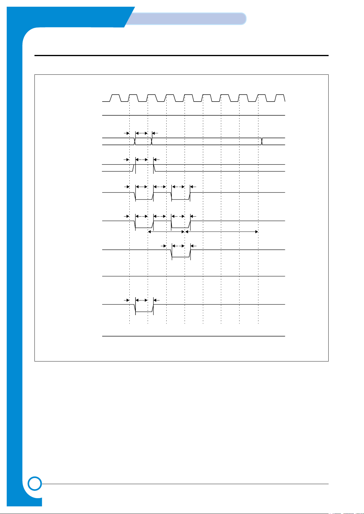
3-3-2-6 P ARALLEL PORT INTERFACE division
S3C46MOX(Jupiter3) has the Parallel Port Interface part
enabling Parallel Interface with PC.
This part is connected to PC through Centronics Connector
in this system, which consists of /ERROR, PE, BUSY,
/ACK, SLCT, /INIT, /SLCTIN, /AUTOFD, /STB and 245DIR
as the part generating the main control signal used to drive
PARALLEL COMMUNICATION. Data transmission
method between this part and PC supports the method
specified in P1284 Parallel Port Standard
(http://www.fapo.com/ieee1284.html) of IEEE.
That is, the Compatibility mode, the fundamental transmission method of print data, supports the Nibble Mode(4bits
data) supporting the Data Uploading to PC, Byte
Mode(8bits data), and ECP(Enhanced Capabilities Port : 8
bits data transmission & receiving) supporting two-way
high speed transmission to PC. The Compatibility mode
and ECP mode may be simply explained as follows.
The Compatibility mode is generally called Centronics
mode and is the protocol used for transmitting data by most
of PC. The ECP mode provides two-way high speed communication as the protocol suggested for improved communication with peripheral equipments such as printer and
scanner.
The ECP mode provides two types of cycles in two-way
transmission. They are data and command cycles.
Command cycle again has Run-length count and Channel
addressing types.
First, RLE (Run Length Encoding) type, having 64-fold
compressibility , is available for the real time data compression, and is used usefully for printer and scanner, which
have to transmit large capacity of raster image having a
series of same data. Next, Channel Addressing is proposed for addressing single structure of multi-device.
For example, although the printer channel is processing
the printer image when the fax/printer/scanner have one
structure like this system, they may use parallel port for
another use. This system does not apply to the parallel port
Interface.
3-12
CIRCUIT DESCRIPTION
Samsung Electronics
Repair Manual
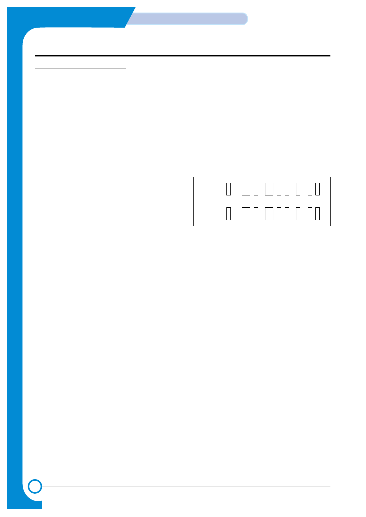
<Figure 10. Compatibility Hardware Handshaking Timing>
1. Write the data to the data register.
2. Program reads the status register to check that the printer is not BUSY.
3. If not BUSY, then Write to the Control Register to assert the STROBE line.
4. Write to the Control register to de-assert the STROBE line.
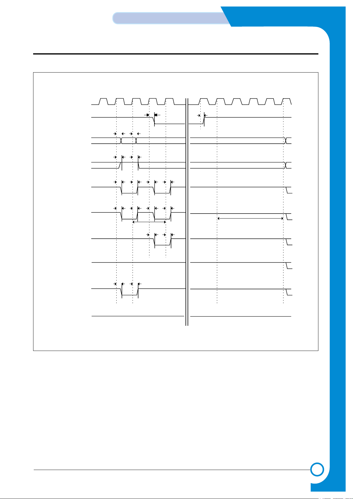
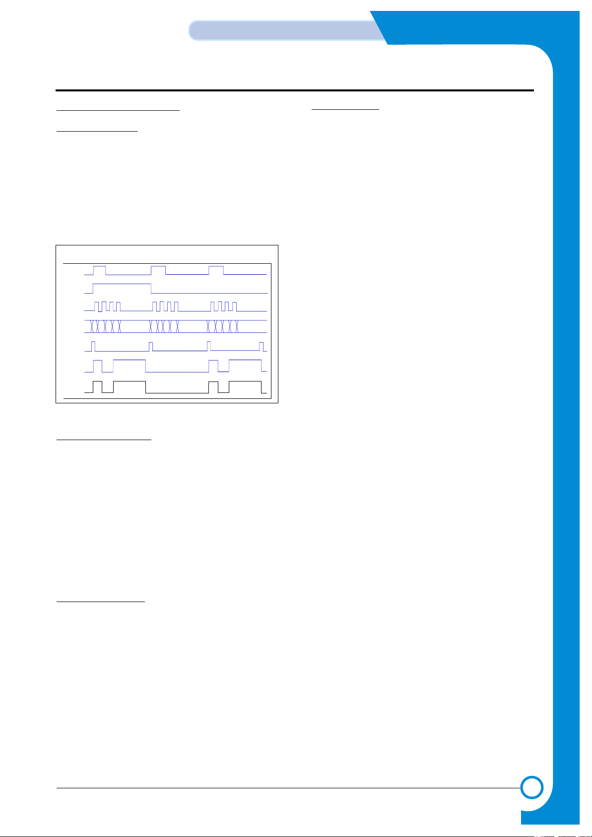
<Figure 10-1. ECP Hardware Handshaking Timing (forward)>
1. The host places data on the data lines and indicates a data cycle by setting nAUTOFD.
2. Host asserts nSTROBE low to indicate valid data.
3. Peripheral acknowledges host by setting BUSY high.
4. Host sets nSTROBE high. This is the edge that should be used to clock the data into the Peripheral.
5. Peripheral sets BUSY low to indicate that it is ready for the next BYTES.
6. The cycle repeats, but this time it is a command cycle because nAUTOFD is low.
BYTE 0 BYTE 1

3-13
Samsung Electronics
CIRCUIT DESCRIPTION
Repair Manual
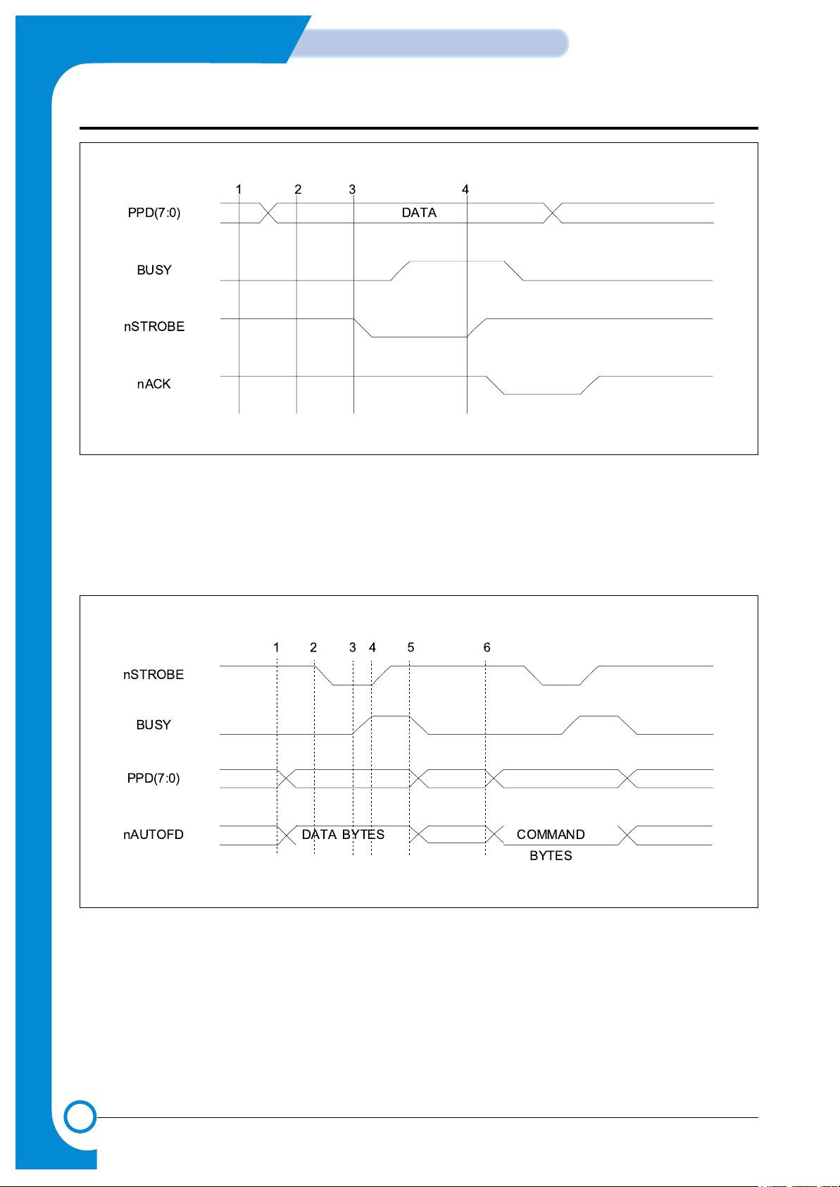
<Figure 10-2. ECP Hardware Handshaking Timing (reverse)>
1. The host request a reverse channel transfer by setting nINIT low.
2. The peripheral signals that it is OK to proceed by setting PE low.
3. The peripheral places data on the data lines and indicates a data cycle by setting BUSY high.
4. Peripheral asserts nACK low to indicate valid data.
5. Host acknowledges by setting nAUTOFD high.
6. Peripheral sets nACK high. This is the edge that should be used to clock the data into the host.
7. Host sets nAUTOFD low to indicate that it is ready for the next BYTES.
8. The cycle repeats, but this time it is a command cycle because BUSY is low.
BYTE 0 BYTE 1
3-14
CIRCUIT DESCRIPTION
Samsung Electronics
Repair Manual
3-3-2-7 USB INTERFACE PART
1. USB function description
As the mode of implementing low cost express PC
Interface, USB was applied. At USB, PC plays the role of
route hub simultaneously by existing in the highest level as
the host. That is, the device supporting each USB is connected centering on PC.
The device is available for Interface for the maximum of
127. USB cable is composed of total of a set of twisted pair
and 2 power lines. Cables have two types.
One is used for express transmission of 12Mbps and may
be extended as long as 5m. The part for implementing USB
function is included in S3C46MOX(Jupiter3).
For Interface of USB, pull-up of 15KΩ is interfaced to the
data line of high level instruments, and, among data lines
of lower level instruments, pull-up resistance of 1.5KΩ is
interfaced to any one.
At this time, D+ line is pulled up for Full Speed device, and,
for Low Speed device, D-line is pulled up. For upper level
instruments(Host, HUB) speed of device is classified interfaced to low level by detecting any one among D+ and D-.
If both lines are in the level of GND at the same time, device
is judged that low device is not interfaced. In the transmission mode of USB, there are
(1) Control transmission,
(2) Interrupt transmission,
(3) Bulk transmission, isochronous transmission
.
Control transmission is for Host to find out configuration
information from USB device. This is conducted when
device is interfaced. Interrupt transmission is used when
small quantity of data is sent periodically. Interval value
may be known from device in the case of initial setting. Bulk
transmission is valid in case of trying to transmit data in
large quantities or in case of transmitting them accurately.
Isochronous transmission should be assured of bandwidth,
and is used when transmitting large quantities of information. Data in voice is used where delay is not allowed but
small error is allowed. At USB coding mode and bit stepping are being conducted. First, in case original data is 1,
bit shall not change, and only when original data is 001, it
shall be inverted. Only while data is 1, 1 and 0 shall be
repeated. Also, in case 1, original data, is continued in 6 bit,
0 shall be inserted, Also, in the 1st phase of packet, data in
the synchronized pattern shall be sent. About more
detailed information regarding USB, see
http//:www.usb.org.
2. operation description
This system, when Host and USB cables are connected,
and when +5V is detected in power detector inside chip
and Vbus(U15-98), 3.3V comes out through Pull-uP terminal. This is also connected to D+ in pattern of hardware and
supports Full-speed. Utilizing Configuration Endpoint,
EPO, in USB controller, Plug & Play function is operated.
Exchange of information between PCs is accomplished
through D+(U15-95) and D-(U15-96) terminals. This terminal decides transmission speed depending on connection
of regulator output in USB controller, and decides size of
signal following USB and SPFC. Signal of general D+ and
D- terminals are same as Figure 10-3.
D+
D-
< Figure 10-3. USB Signal Line DIAGRAM >
3-15
Samsung Electronics
CIRCUIT DESCRIPTION
Repair Manual
3-3-2-8 HEAD control part
1. Entire description
As part to drive INKJET HEAD, it is composed of ACLK,
AGATE, LDCS, LATCHCTL, PCLK, PDATA[3:0], PLOAD,
PENABLE signals for controlling Spitfire of CR B’D generating signal, which is driving Nozzle of Head, and
PH_ID[1:0] and OK2Print signals receiving from Spitfire.
Here,HEAD being used here is DOUBLE HEIGHT PRINT
HEAD, and MONO is configured with 208 NOZZLE, and
COLOR is with 192 NOZZLE.
<Figure 11 HEAD Control Part Timing Diagram>
2. A-LINE driving circuit
13 Address Lines are input into 13 Address Counters in
sequence at Rising edge of ACLK signal, which is input
serially into Spitfire. Output of this Counter was connected
to each A-line driver, and this driver output becomes A-line
signal. The sequence of signal input into Address Counter
is decided by ADIR, and if it is ADIR=0, it is input in
sequence of A13A1, and if it is ADIR=1, in sequence of A1
=> A13. AGATE signal is used to reset Address Counter. If
it becomes AGATE=1, A-Line output becomes Low state.
The cycle of ACLK is 1.5ß¡ in minimum, and Sink current of
each Driver is 60mA.
3. P-LINE drive circuit
P-Line values are clocked to 4-bit Serial to Parallel Shift
Register Clock in Spitfire ASIC, and ASIC shall clock-in Pline NO. of fitting value at Rising Edge of PCLK. These values are latched to Holding register at Rising Edge of
PLOAD. PLOAD Pulse Duration is 50n, and P-line value of
Holding Register is done AND with PENABLE signal in
order to generate appropriate Fire Pulse. PLCK is available
for handling as much as 4MHz. Drive Current of P-line is
400mA. Data of P1°≠P4 is shifted to PDATAO, that of P5P8 shifted to PDATA1, that of P9-P12 shifted to PDATA2,
and that of P13-P16 shifted to PDATA3.
4. Control Signal
• The signal loaded on PDATAO - PDATA2 at Rising edge
of LATCHCTL(Latch Control Nibble) is used as function
as follows in Spitfire.
- PDATA0 == ADIR —> Low : ACLK is operated in Count
Down, High : ACLK is operated in Count
Up.
- PDATA1 == When Fault Test —> High, check whether
P-Line of Head became short with GND.
- PDATA2 == When Print Head ID Check —> high,
make sure that Check mode is set, and,
after that, by using the PDATA0~PDATA2
LIne, make A1-A3 signal for sending, and
Head ID shall come out with PH_IDn output. At this time ID could be displayed only
if each Substrate heater is turned on.
• The signal loaded into PDATAO-PDATA3 at Rising
edge of LDCS(LoadHtrcs) signal is used in the following functions in Spitfire.
- PDATA0 == BLKHTR—> High : Turn on Substrate
Heater of Mono Head.
- PDATA1 == COLHTR—> High : Turn on Substrate
Heater of Color Head.
- PDATA2 == nHSM—> Low : Enable Select Signal of
Mono Head.
- PDATA3 == nHSC—> Low : Enable Select Signal of
Color Head.
When Substrate Heater is turned on, Over-current Check
circuit is operated, automatically , and,if the current is above
750mA, the printer stops operation after OK2PRT
becomes low.
The Timing diagam below shows signal timin for the P-line block
ACLK
An
PCLK
PDATA
PLOAD
PENABLE
Pn
3-16
CIRCUIT DESCRIPTION
Samsung Electronics
Repair Manual
3
-3-2-9 SYNCHRONOUS SERIAL INTERFACE part
As the part interfacing with THUNDERBOLT ASIC, it consists of /TBCS,TBCLK,TBDO. In sending SERIAL DATA
of 13 BIT to Thunderbolt ASIC, meaning of each bit is as
follows. BIT 1 is the bit to do On/Off VPH(+11.82V), BIT
[2:7] is the bit for driving MOTOR 1, BIT [8:13] is the bit to
drive MOTOR 2. MOTORs are available for being used as
STEPPER MOTOR and DC MOTOR respectively.
3-3-2-10 MOTOR control part
(DIR, PWM, LFPHA,LFPHB, LFIA[0:1],
LFIB[0:1])
S3C46MOX(Jupiter3) is arranged to support one Step
motor and one DC motor. This system does not use the
Motor control part provided by S3C46MOX(Jupiter3).
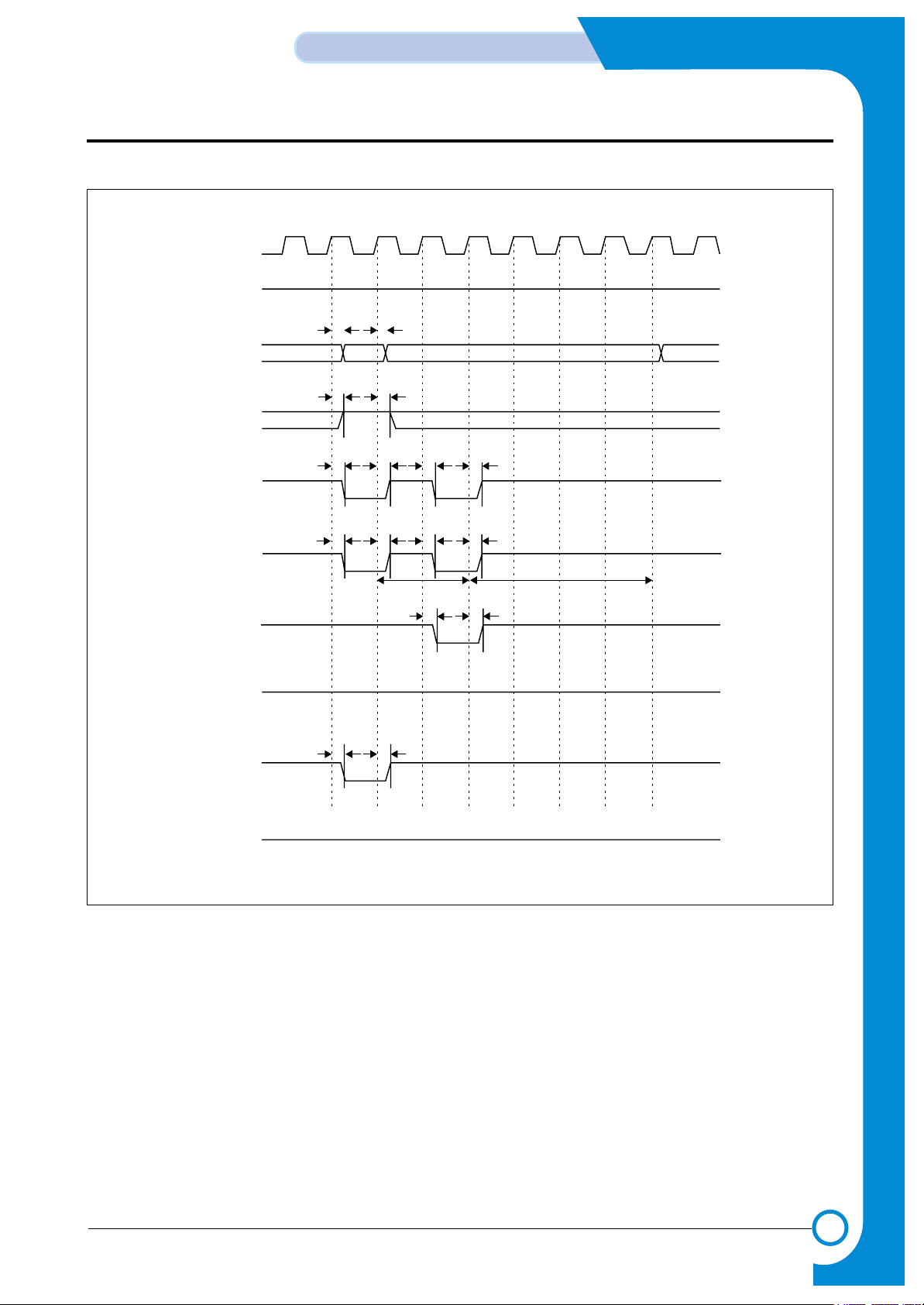
< Figure 12 SYNCHRONOUS SERIAL INTERFACE TIMING DIAGRAM >
/TBCS
TBCLK
TBDO
Tcs-sclk
Tcs-sclk
bit 1 bit 2 bit 3 bit 4 bit 5 bit 6 bit 7 bit 8 bit 9 bit 10 bit 11 bit 12 bit 13
SDI stays at
last value
MSBLSB
Data Latcked on the rising edge of SCLK
time
Tdhd
Tdsu
STEPPER MOTOR DC MOTOR
BIT 1 VPH_ENABLE VPH_ENABLE
BIT 2 MOTOR1_CURR_I1_PHASEB Not used in this mode.
BIT 3 MOTOR1_CURR_I0_PHASEB Not used in this mode.
BIT 4 MOTOR1_DIR_PH_B Not used in this mode.
BIT 5 MOTOR1_CURR_I1_PHASEA Not used in this mode.
BIT 6 MOTOR1_CURR_I0_PHASEA Not used in this mode.
BIT 7 MOTOR1_DIR_PH_A MOTOR1_DIRECTION
BIT 8 MOTOR2_CURR_I1_PHASEB Not used in this mode.
BIT 9 MOTOR2_CURR_I0_PHASEB Not used in this mode.
BIT 10 MOTOR2_DIR_PH_B Not used in this mode.
BIT 11 MOTOR2_CURR_I1_PHASEA Not used in this mode.
BIT 12 MOTOR2_CURR_I0_PHASEA Not used in this mode.
BIT 13 MOTOR2_DIR_PH_A MOTOR2_DIRECTION
3-17
Samsung Electronics
CIRCUIT DESCRIPTION
Repair Manual
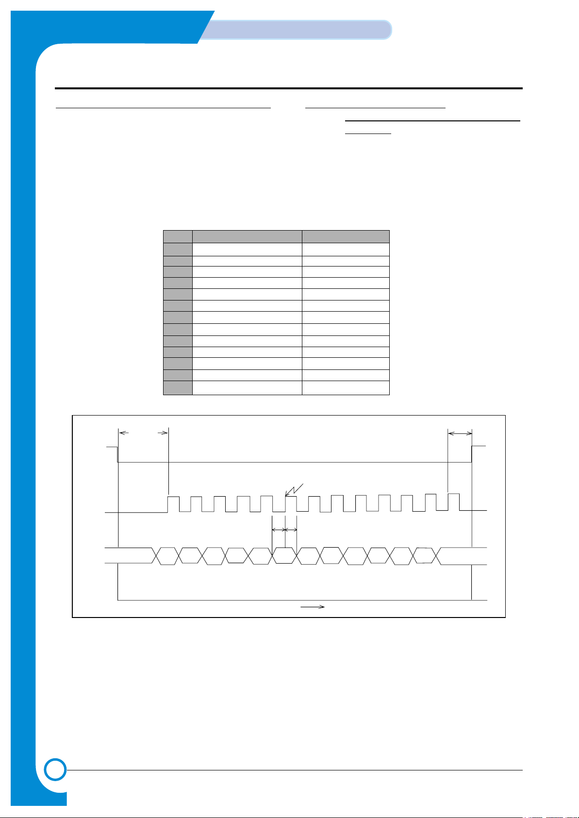
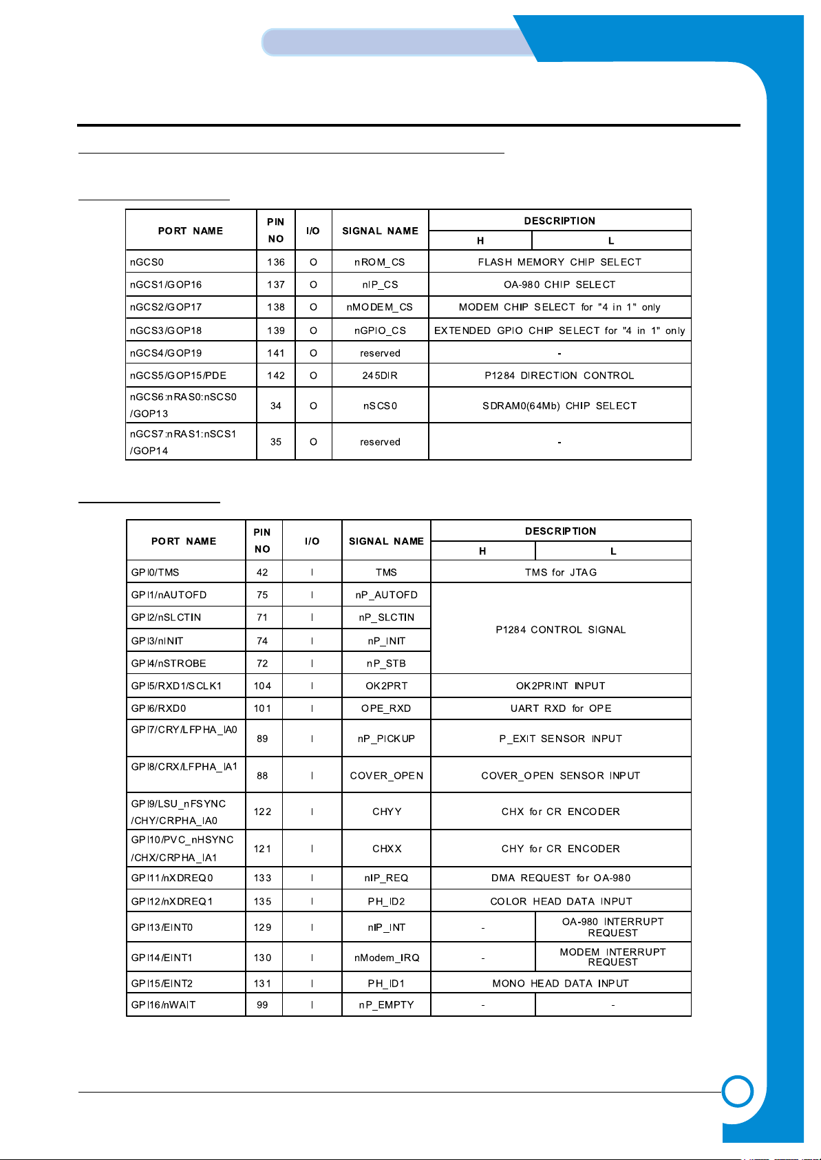
3-3-2-11 GENERAL PURPOSE I/O PORT of S3C46MOX(Jupiter3)
1. J3 Assigned GCS Ports
2. J3 Assigned GPI Ports
 Loading...