

Page 1
Repair Manual
Repair Manual
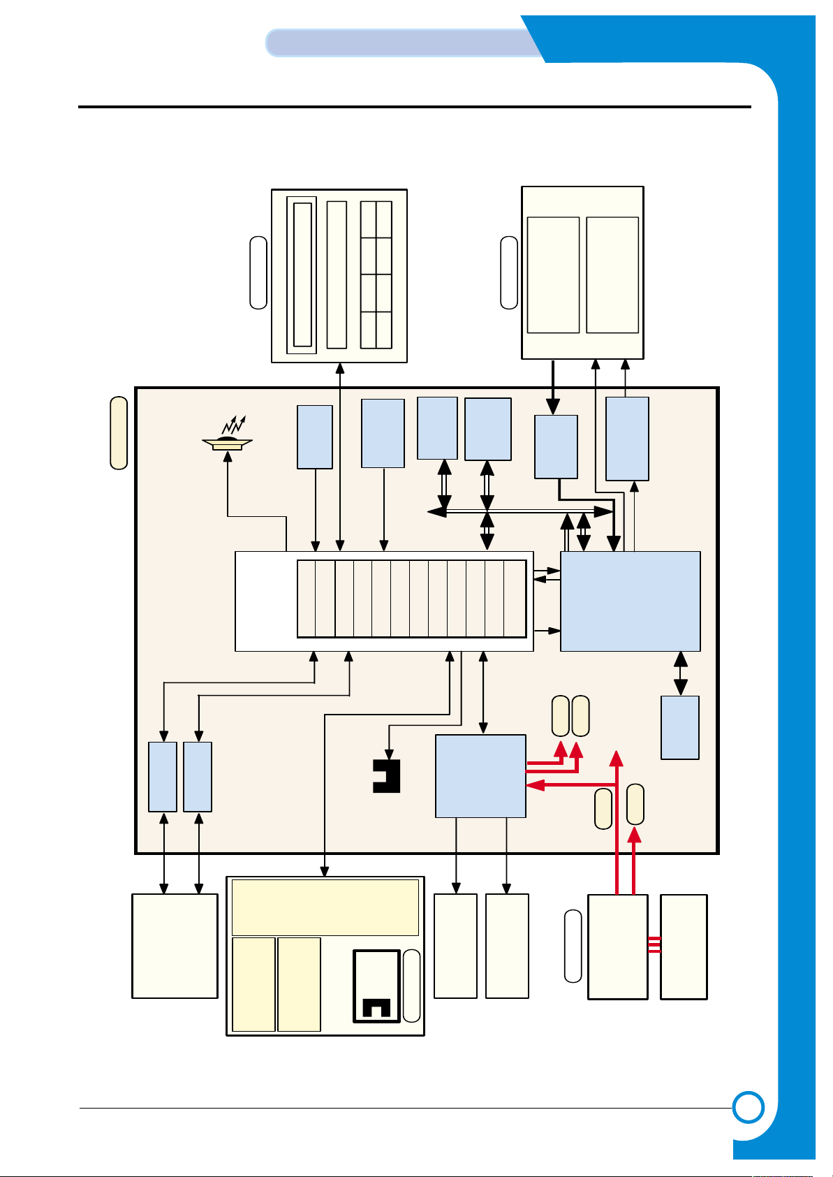
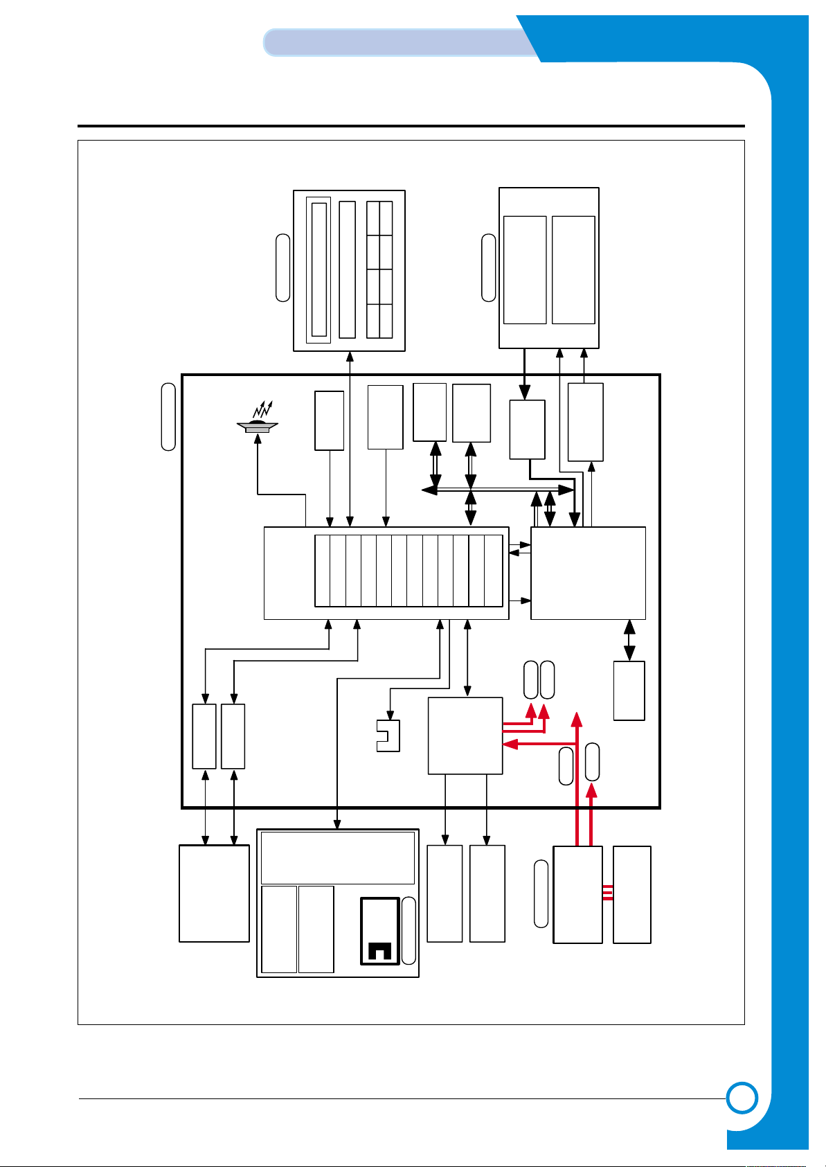
1. Block Diagram
2. Connection Diagram
3. Circuit Description
4. Schematic Diagrams
CONTENTS
INKJET RINTER(MFP)
SCX-1100
Page 2
1
1-1
Samsung Electronics
BLOCK DIAGRAM
Repair Manual
1. Block Diagram
SMPS
(15)
Main
Controller
(U21)
Image
Processor
OA-980
Main Clock
10MHz
RESET
CONTROLLER
FLASH ROM
ADC
16bit
(U16)
SDRAM
1M* 16bit
(U9)
CARRIER
MOTOR
LINE FEED
MOTOR
(30V, 3.3V)
AC
(110~240V)
CCD Module
( COLOR 600DPI )
SCAN MOTOR
( Bi-POLAR STEP )
SCAN STEPPER
MOTOR DRIVER
COLOR
CARTRIDGE
MONO
CARTRIDGE
PRINT HEAD(2PEN)
60DPI DOUBLE HEIGHT
ENCORDER
SENSOR
ENCODER
USB CONN
PC
48MHz
(AU1)
BUZZER
(U27)
SDRAM
(4M 16bit)
1284 CONN
(U1)
HEAD
Driver
IC
/REQ /ACK
KEY PANNEL
LCD
Mcro Controller (U1)
(U5)
(U10,U14)
POWER
MAIN
OPE
SCANNER
+30V
+5V
+12V
+3.3V
PAPER EXIT
SENSOR
(U4)
Motor
Driver
& Regul at or
(U13)
(U7)
ARM7TDM
MEM CNTR
Head Control I/F
SCAN CNTR
DERASTERIZER
UART 3
IEEE 1284
TIMERS
I/O PORT
INT. CNTR
USEB
DM 2
Page 3

2
2-1
Samsung Electronics
CONNECTION DIAGRAM
Repair Manual
2. Connection Diagr am
• Reffer to the Schematic diagram(see page 4-2)
Page 4
3
3-1
Samsung Electronics
CIRCUIT DESCRIPTION
Repair Manual
3. Circuit Description
3-1. GENERAL DESCRIPTION
Main circuit consists of mainly consists of CPU and the controller part with various types of built-in I/O device driver(built-in
RISC Processor Core: ARM7TDMI), system memory part, OA980 controlling input of image received from media and con version, CF(COMP ACTstorage card) interface part. The following nomenclatures by section is the same as those listed in
the circuit diagram.
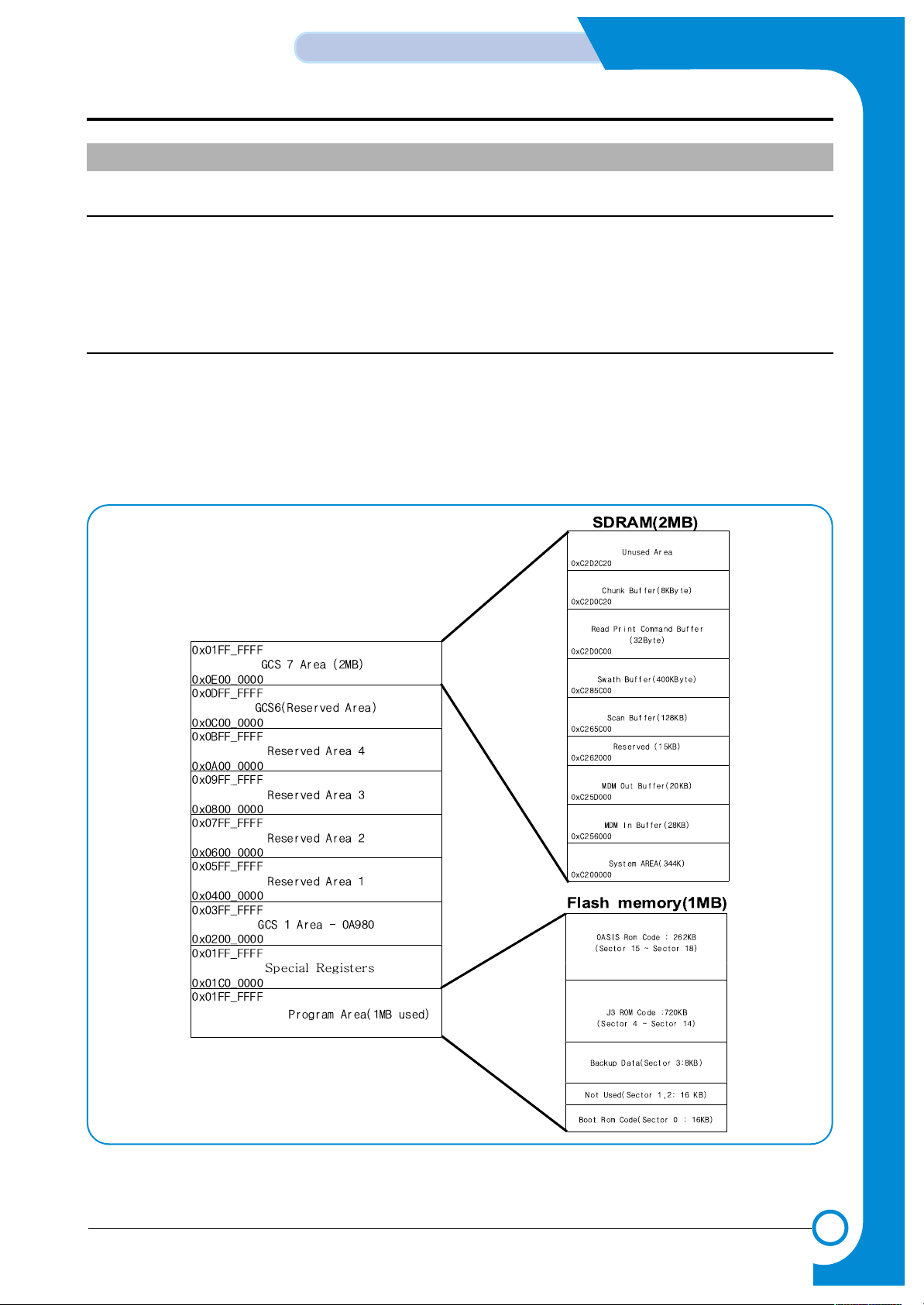
3-2. MEMORY MAP
The entire Addressing area provided by MAIN CONTROLLER(S3C46MOX(Jupiter3)) is 256MBytes from 0x00000000 to
0x10000000, and the Max. Address Range for each External Chip Select is 32M Byte or Half word from 0x000000 to
0x01FFFFFF and embodied with Big-Endian Bus interface. MEMORY area is divided into EXTERNAL ROM and RAM
areas(See (Figure 1)), and the areas actually used are 2M/8M BYTES SDRAM and 1M BYTES ROM(FLASH MEMORY).
In case of SDRAM, it uses 0xC200000h ~ 0xC3FFFFFh(2MB), and ROM uses 0x0000000h ~ 0x0FFFFFh area.
<Figure 1. S3C46MOX(Jupiter3) MEMORY MAP>
◊ MAIN PBA
Page 5
3-2
CIRCUIT DESCRIPTION
Samsung Electronics
Repair Manual
3-3.DETAILED DESCRIPTION
3-3-1 BLOCK DIAGRAM and MAIN CONTROLLER description
3-3-1-1 GENERAL DESCRIPTION
MAIN CONTROLLER(S3C46MOX(Jupiter3),U15) consists of this system consists of CPU(ARM7TDMI RISC PROCESSOR), 8K BYTES CACHE, DATAand ADDRESS BUS, PLLderiding input frequency and CLOCK CONTROL part,
SERIAL COMMUNICATION part supporting UART, PRINT HEAD control part, PARALLELPORT INTERFACE part,
USB INTERFACE part, External DMApart for receiving data from external COLOR IMAGE PROCESSOR(OA980,U21), MEMORY and EXTERNAL BANK control part, SYNCHRONOUS SERIAL INTERFACE control part for interfacing Thunderbolt, and LF/CR Motor drive control and general purpose I/O control parts.(See Figure 2 )
3-3-2 S3C46MOX(Jupiter3) FUNCTION DESCRIPTION
3-3-2-1 SYSTEM CLOCK
There are two ways of Clock input method. One is the method to make Master Clock(MCLK) at the internal PLLby connecting X-tal and Capacitor to the outside, and another method is to use MCLK(When inputting 40MHz) directly, which
supplies maximum 40MHz Clock to the EXTCLK terminal(PIN65). The range of frequency being input in case of using
X-tal is limited to 4MHz~10MHz. This system uses SSCG(FS781) with a 10MHZ X-tal outside to make MCLK, and supplies Clock to the XIN terminal(PIN67) of ASIC by expanding Spectrum with bandwidth about 1.5% in comparison with
the basic frequency by using this IC. Inside the ASIC, the PLL makes 66MHz MCLK signal, which is the basic operation
frequency of the System. Also, this PLLmakes 48MHz, the operation frequency of USB Controller.
3-3-2-2 DATAAND ADDRESS BUS CONTROL
1. /RD & /WR
/RD & /WR SIGNAL are synchronized with the inside MCLK(66MHZ) and becomes active to Low.
These signal are Strobe Signal used to Read or Write data when each Chip Select becomes active connected to
/RD,/WR PIN of RAM, ROM, OA-980.
2. CHIP SELECT (/ROMCS, /IP_CS,/MED_CS,/SCS0,/SCS1)
- /ROMCS : FLASH MEMORY(U7) CHIP SELECT (LOW ACTIVE)
- /IP_CS : OA-980(U21) CHIP SELECT
(LOW ACTIVE)
- /SCS1 : SDRAM(OPTION)(U12) CHIP SELECT(LOW ACTIVE)
In case each Chip Select is low, it may Read or Write data.
3. D0 ~ D15
- 16BIT DATA BUS
4. A0 ~ A24
- ADDRESS BUS (A23 ~ A24 RESERVED)
Page 6
3-3
Samsung Electronics
CIRCUIT DESCRIPTION
Repair Manual
<Figure 2. Block Diagram of Main Part>
SMPS
(15)
Main
Controller
(U21)
Image
Processor
OA-980
Main Clock
10MHz
RESET
CONTROLLER
FLASH ROM
ADC
16bit
(U16)
SDRAM
1M* 16bit
(U9)
CARRIER
MOTOR
LINE FEED
MOTOR
(30V, 3.3V)
AC
(110~240V)
CCD Module
( COLOR 600DPI )
SCAN MOTOR
( Bi-POLAR STEP )
SCAN STEPPER
MOTOR DRIVER
COLOR
CARTRIDGE
MONO
CARTRIDGE
PRINT HEAD(2PEN)
60DPI DOUBLE HEIGHT
ENCORDER
SENSOR
ENCODER
USB CONN
PC
48MHz
(AU1)
BUZZER
(U27)
SDRAM
(4M 16bit)
1284 CONN
(U1)
HEAD
Driver
IC
/REQ /ACK
KEY PANNEL
LCD
Mcro Controller (U1)
(U5)
(U10,U14)
POWER
MAIN
OPE
SCANNER
+30V
+5V
+12V
+3.3V
PAPER EXIT
SENSOR
(U4)
Motor
Driver
& Regul at or
(U13)
(U7)
ARM7TDM
MEM CNTR
Head Control I/F
SCAN CNTR
DERASTERIZER
UART 3
IEEE 1284
TIMERS
I/O PORT
INT. CNTR
USEB
DM 2
Page 7
3-4
CIRCUIT DESCRIPTION
Samsung Electronics
Repair Manual
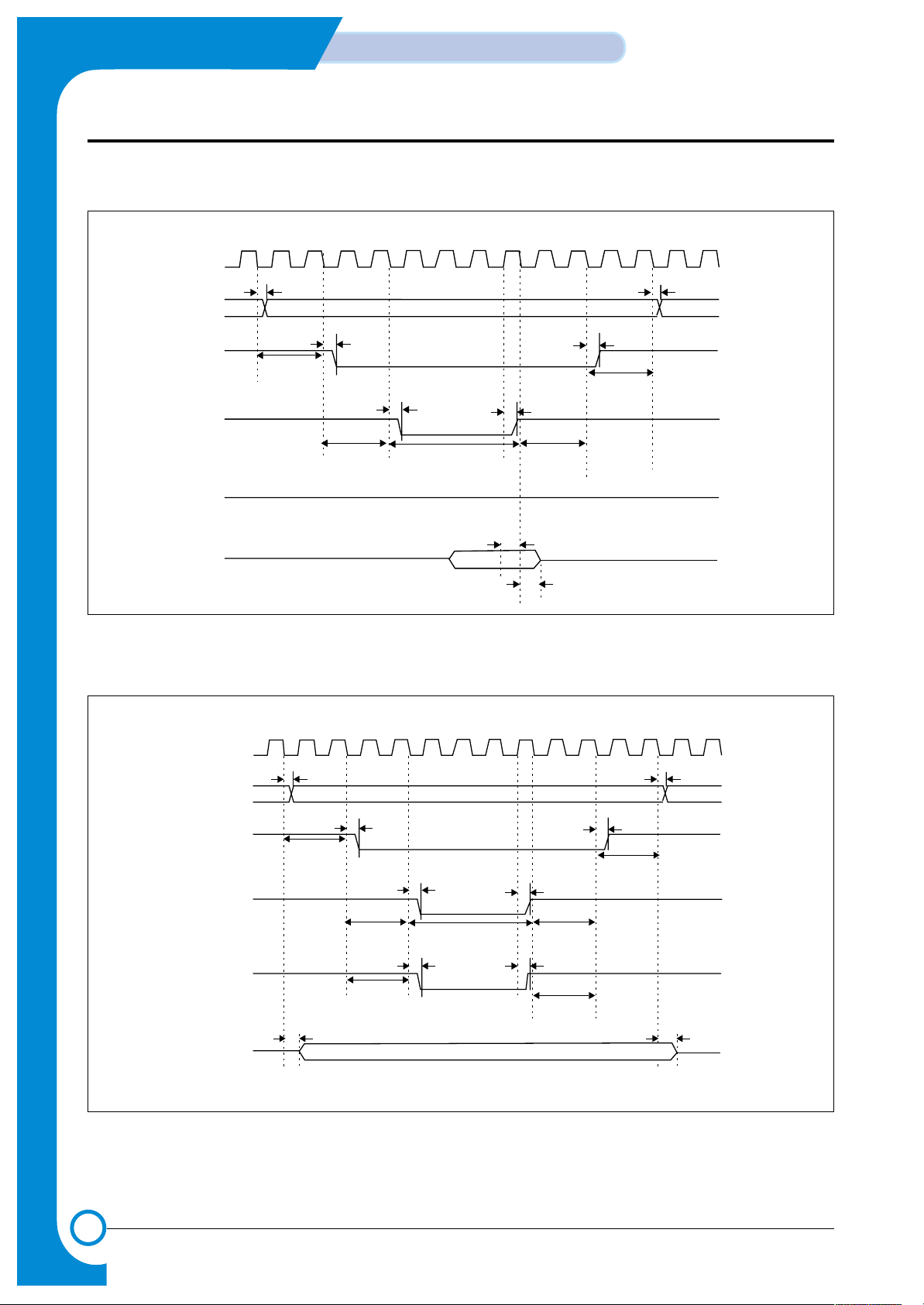
<Figure 3. Flash Memory Read Timing>
<Figure 4. Flash Memory Write Timing>
EXTCLK
nGCSx
nGCSx
ADDR
tRWD
tRAD
Tacs
tRCD
nWE
DATA
nBEx
Tacc
Toch
Tcah
Tocs
tRCD
tRWD
tRDD
tRAD
tRDH
’1’
EXTCLK
ADDR
nGCSx
nWE
nGCSx
nBEx
DATA
tRAD
tRCD
Tacs
tRWD
Tocs
tRWBED
Tcos
tRDD
Tacc
tRAD
tRCD
Tcah
tRWD
Toch
tRWBED
Toch
tRDD
Page 8
3-5
Samsung Electronics
CIRCUIT DESCRIPTION
Repair Manual
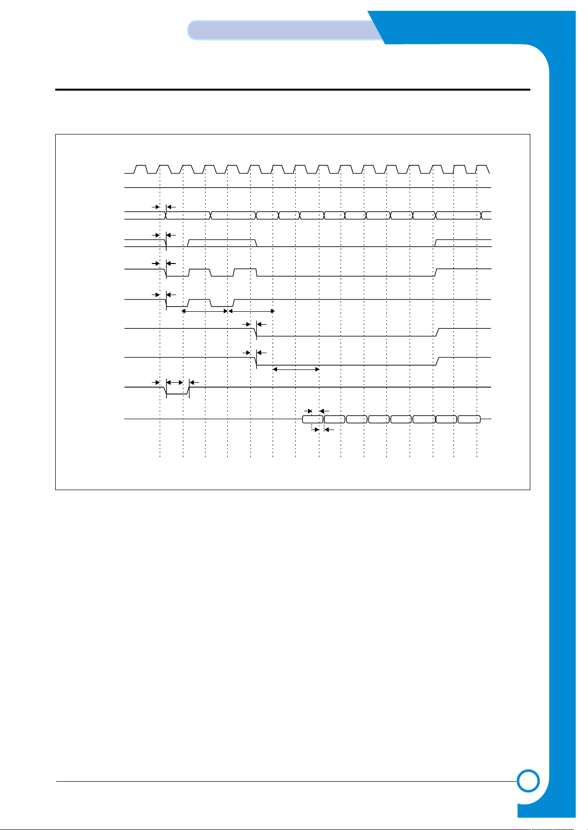
<Figure 5. SDRAM Read Timing>
SCLK
SCKE
ADDR/BA
AP/A10
nGCSx
nSRAS
nSCAS
nBEx
nWE
DATA
’1’
tSAD
tSAD
tSCSD
tSRD
Trp Trcd
tSCD
tSBED
Tcl
tSWD
tSDS
tSDH
Page 9
3-6
CIRCUIT DESCRIPTION
Samsung Electronics
Repair Manual
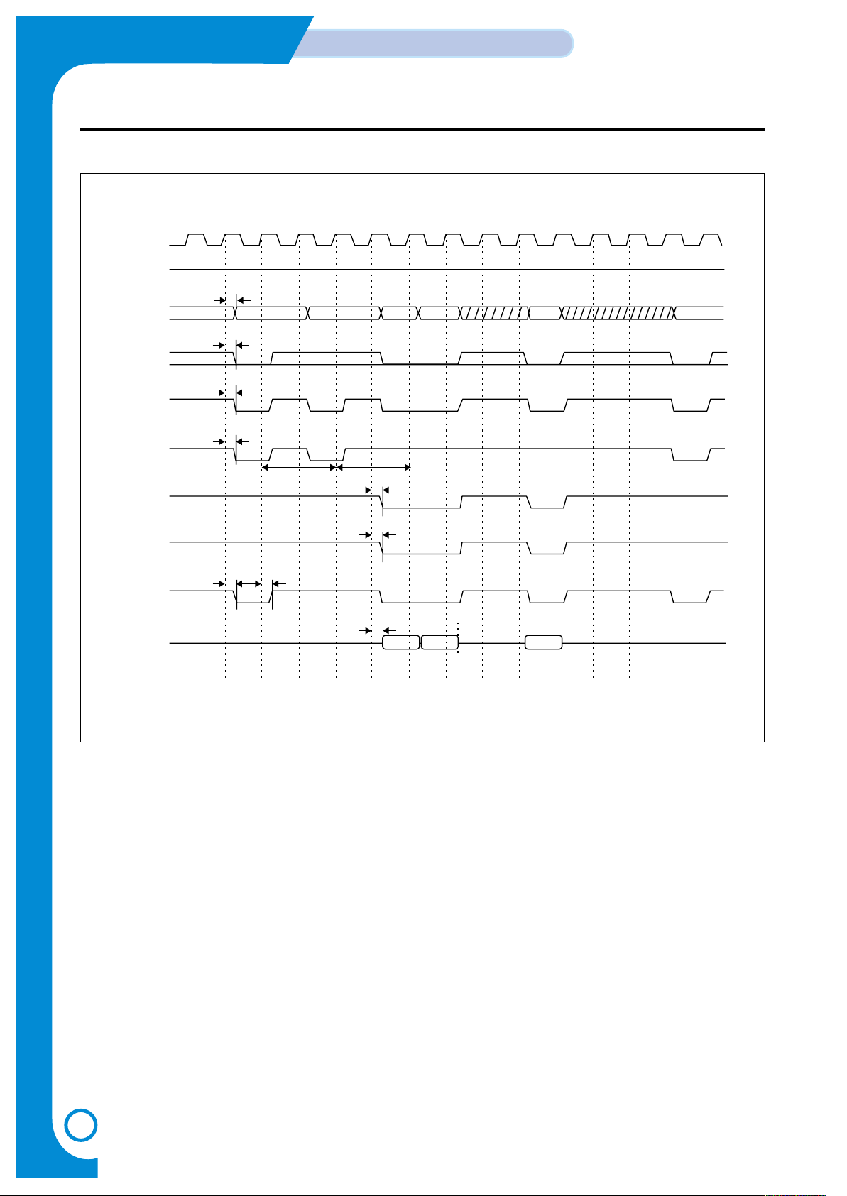
<Figure 6. SDRAM Write Timing>
SCLK
’1’
SCKE
ADDR/BA
AP/A10
nGCSx
nSRAS
nSCAS
nBEx
nWE
DATA
tSAD
tSAD
tSCSD
tSRD
Trp
Trcd
tSWD
tSDD
tSDD
tSBED
tSCD
Page 10

3-7
Samsung Electronics
CIRCUIT DESCRIPTION
Repair Manual
<Figure 7. SDRAM Write Timing>
SCLK
SCKE
ADDR/BA
AP/A10
nGCSx
nSRAS
nSCAS
nBEx
nWE
DATA
tSAD
’1’
’1’
’HZ’
tSAD
tSCSD
tSRD tSRD
tSCD
tSWD
tSCSD
tSAD
Trp Trc
Page 11
3-8
CIRCUIT DESCRIPTION
Samsung Electronics
Repair Manual
<Figure 8. SDRAM auto Refresh Timing>
SCLK
SCKE
ADDR/BA
AP/A10
nGCSx
nSRAS
nSCAS
nBEx
nWE
DATA
tSAD
’1’
’1’
’HZ’
tSAD
tSCSD
tSRD tSRD
tSCD
tSWD
tSCSD
tSAD
Trp Trc
Page 12
3-9
Samsung Electronics
CIRCUIT DESCRIPTION
Repair Manual
<Figure 9. SDRAM Self Refresh Timing>
SCLK
SCKE
ADDR/BA
AP/A10
nGCSx
nSRAS
nSCAS
nBEx
nWE
DATA
’HZ’
tSWD
’HZ’
’1’
’1’
’1’
’1’
’1’
’1’
’1’
tCKED
tSAD
tSAD
tSCSD
tSRD tSRD
tSCD
tSCSD
tSAD
tCKED
Trc
Trp
Page 13
3-10
CIRCUIT DESCRIPTION
Samsung Electronics
Repair Manual
Parameter Symbol Min T yp. Max Unit
ROM/SRAM Address Delay
t
RAD - 12 - ns
ROM/SRAM Chip select Delay
t
RCD - 11 - ns
ROM/SRAM Output enable Delay
t
ROD - 1 1 - ns
ROM/SRAM read Data Setup time
t
RDS - 1 - ns
ROM/SRAM read Data Hold time
t
RDH - 5 - ns
ROM/SRAM Byte Enable Dalay
t
RBED - 13 - ns
ROM/SRAM Write Byte Enable Delay
t
RWBED - 14 - ns
ROM/SRAM output Data Delay
t
RDD - 14 - ns
ROM/SRAM external Wait Setup time
t
WS - 1 - ns
ROM/SRAM external Wait Hold time
t
WH - 5 - ns
ROM/SRAM Write enable Delay
t
RWD - 14 - ns
DRAM Address Delay
t
DAD - 12 - ns
DRAM Row active Delay
t
DRD - 11 - ns
DRAM Read Column active Delay
t
DRCD - 1 1 - ns
DRAM Output enable Delay
t
DOD - 12 - ns
DRAM read Data Setup time
t
DDS - 1 - ns
DRAM read Data Hold time
t
DDH - 5 - ns
DRAM Write Cas active Delay
t
DWCD - 14 - ns
DRAM Cbr Cas active Delay
t
DCCD - 12 - ns
DRAM Write enable Delay
t
DWD - 13 - ns
DRAM output Data Delay
t
DDD - 14 - ns
SDRAM Address Delay
t
SAD - 4 - ns
SDRAM Chip Select Delay
t
SCSD - 4 - ns
SDRAM Row active Delay
t
SRD - 4 - ns
SDRAM Column active Delay
t
SCD - 4 - ns
SDRAM Byte Enable Delay
t
SBED - 5 - ns
SDRAM Write enable Delay
t
SWD - 5 - ns
SDRAM read Data Setup time
t
SDS - 4 - ns
SDRAM read Data Hold time
t
SDH - 0 - ns
SDRAM output Data Delay
t
SDD - 8 - ns
SDRAM Clock Eable Delay
t
CKED - 5 - ns
< ROM/SRAM Bus Timing Constants >
(V
DDP
: 3.3V, V
DDI
: 2.5V, Ta =25˚C, PLCAP=70pf, Max/Min=typ. ±30%)
Page 14

3-11
Samsung Electronics
CIRCUIT DESCRIPTION
Repair Manual
3-3-2-3 EXTERNAL DMA part
The function of this part is to bring data from external
DEVICE(OASIS:U21) by using GENERAL DMA. If DMA
REQUEST(/IP_REQ) is sent from external DEVICE to
S3C46MOX(JUPITER3:U15), DMA ACKNOWLEDGE
SIGNAL(/IP_ACK) is activated and the GENERAL DMAis
driven, so READ STROBE(/RD) in the external DEVICE to
bring data from the external DEVICE requiring CHANNEL.
To transfer this DATAto the DESTINATION MEMOR Y, the
ADDRESS of the DESTINATION MEMORY, CHIP
SELECT and WRITE STROBE(/WR) are generated to
store.
That is, if the EXTERNAL DMAis required by the external
DEVICE, S3C46MOX(Jupiter3:U15) responds to drive the
inside DMA CONTROLLER and then allocate GENERAL
DMA to external CHANNEL so that the data may be transferred to MEMORY TO MEMORY or external DEVICE TO
MEMORY.
• For more details, see the circuit description, see the circuit
description part of IMAGE PROCESSOR (5.3).
3-3-2-4 DRAM control part
Since S3C46MOX(Jupiter3) has the DRAM CONTROLLER build-in, it may be used by connecting DRAM
with external memory.
The Control mode of DRAM CONTROLLER provided by
S3C46MOX(Jupiter3) is available for EARLY WRITE,
NORMAL READ, PAGE MODE, and BYTE/HALF WORD
ACCESS, and is supported even by EDO DRAM,and
SDRAM as well as, Fast page DRAM.
This system uses SDRAM, and the signal used for
READ/WRITE uses /RD,/WR signal used for SYSTEM
BUS CONTROL. It is supported with auto REFRESH and
also by the Self-refresh mode for DRAM
BACK UP. It con-
sists of 2 Banks connected to co
mmon /SCS[1:0], /SCAS,
/SRAS, /SCLK, /SCKE, /DQM[1:0], each of them may use
up to 2M ~ 32M HALF WORD.
In this system, 2 MB is applied as system memory. The
area of DRAM is specified in the DRAM MEMORY MAP of
Fig. 1, while the related TIMING DIAGRAM in Fig. 5, 6, 7,
8, 9.
3-3-2-5 RTC (REAL TIME CLOCK) part
The RTC related circuit part is not applied because the fax
function is not applied, in this system.
3-3-2-6 P ARALLELPORT INTERFACE division
S3C46MOX(Jupiter3) has the Parallel Port Interface part
enabling Parallel Interface with PC.
This part is connected to PC through Centronics Connector
in this system, which consists of /ERROR, PE, BUSY,
/ACK, SLCT, /INIT, /SLCTIN, /AUTOFD, /STB and 245DIR
as the part generating the main control signal used to drive
PARALLEL COMMUNICATION. Data transmission
method between this part and PC supports the method
specified in P1284 Parallel Port Standard
(http://www.fapo.com/ieee1284.html) of IEEE.
That is, the Compatibility mode, the fundamental transmission method of print data, supports the Nibble Mode(4bits
data) supporting the Data Uploading to PC, Byte
Mode(8bits data), and ECP(Enhanced Capabilities Port : 8
bits data transmission & receiving) supporting two-way
high speed transmission to PC. The Compatibility mode
and ECP mode may be simply explained as follows.
The Compatibility mode is generally called Centronics
mode and is the protocol used for transmitting data by most
of PC. The ECP mode provides two-way high speed communication as the protocol suggested for improved communication with peripheral equipments such as printer and
scanner.
The ECP mode provides two types of cycles in two-way
transmission. They are data and command cycles.
Command cycle again has Run-length count and Channel
addressing types.
First, RLE (Run Length Encoding) type, having 64-fold
compressibility , is available for the real time data compression, and is used usefully for printer and scanner, which
have to transmit large capacity of raster image having a
series of same data. Next, Channel Addressing is proposed for addressing single structure of multi-device.
For example, although the printer channel is processing
the printer image when the fax/printer/scanner have one
structure like this system, they may use parallel port for
another use. This system does not apply to the parallel port
Interface.
Page 15
3-12
CIRCUIT DESCRIPTION
Samsung Electronics
Repair Manual
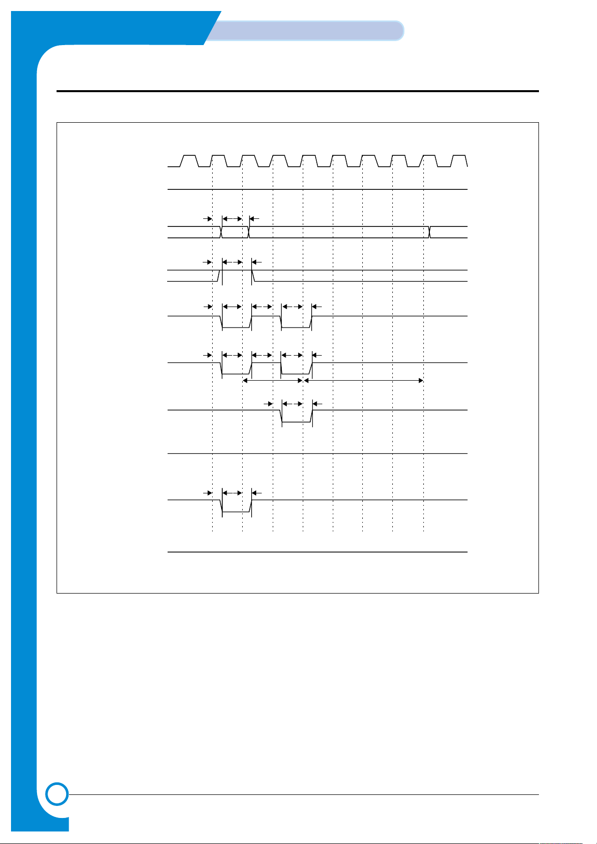
<Figure 10. Compatibility Hardware Handshaking Timing>
1. Write the data to the data register.
2. Program reads the status register to check that the printer is not BUSY.
3. If not BUSY, then Write to the Control Register to assert the STROBE line.
4. Write to the Control register to de-assert the STROBE line.
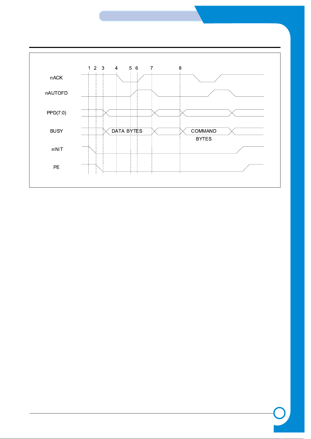
<Figure 10-1. ECP Hardware Handshaking Timing (forward)>
1. The host places data on the data lines and indicates a data cycle by setting nAUTOFD.
2. Host asserts nSTROBE low to indicate valid data.
3. Peripheral acknowledges host by setting BUSY high.
4. Host sets nSTROBE high. This is the edge that should be used to clock the data into the Peripheral.
5. Peripheral sets BUSY low to indicate that it is ready for the next BYTES.
6. The cycle repeats, but this time it is a command cycle because nAUTOFD is low.
BYTE 0 BYTE 1
Page 16
3-13
Samsung Electronics
CIRCUIT DESCRIPTION
Repair Manual
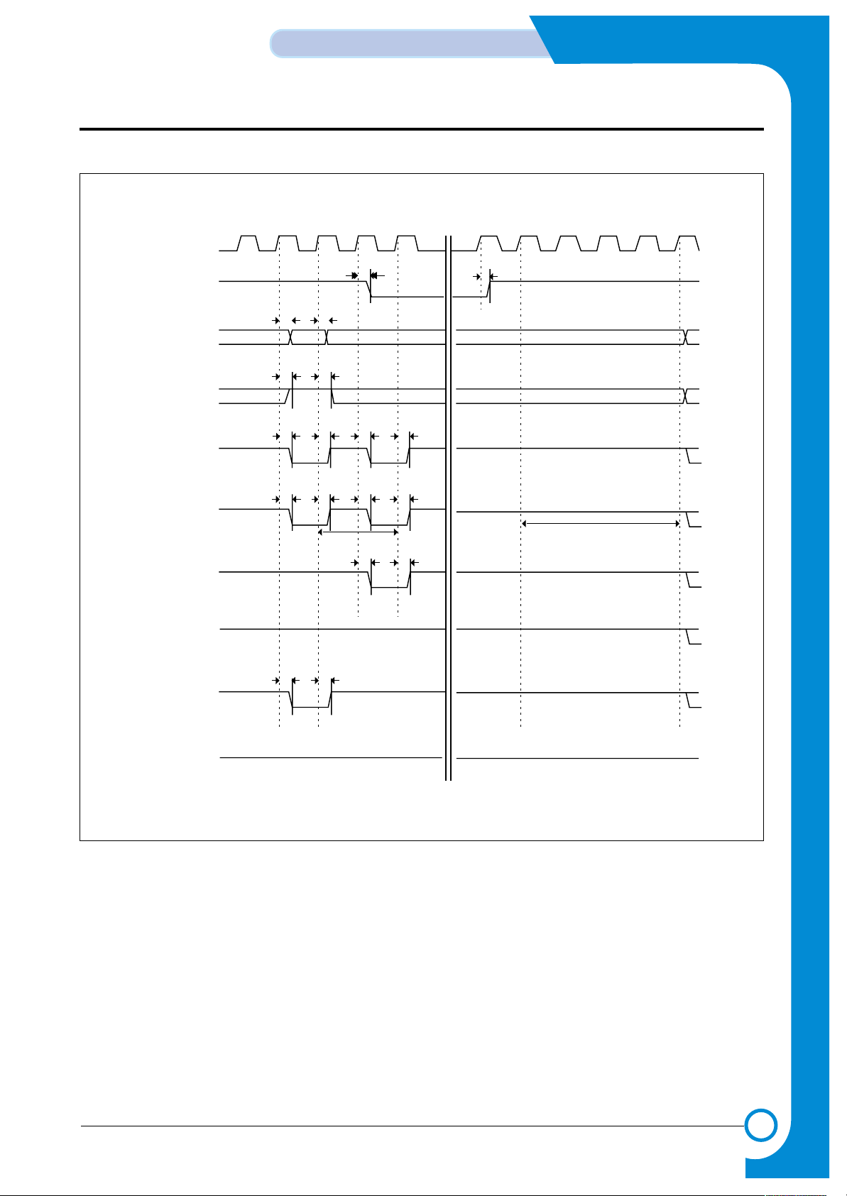
<Figure 10-2. ECP Hardware Handshaking Timing (reverse)>
1. The host request a reverse channel transfer by setting nINIT low.
2. The peripheral signals that it is OK to proceed by setting PE low.
3. The peripheral places data on the data lines and indicates a data cycle by setting BUSY high.
4. Peripheral asserts nACK low to indicate valid data.
5. Host acknowledges by setting nAUTOFD high.
6. Peipheral sets nACK high. This is the edge that should be used to clock the data into the host.
7. Host sets nAUTOFD low to indicate that it is ready for the next BYTES.
8. The cycle repeats, but this time it is a command cycle because BUSY is low.
BYTE 0 BYTE 1
Page 17

3-14
CIRCUIT DESCRIPTION
Samsung Electronics
Repair Manual
3-3-2-7 USB INTERFACE PART
1. USB function description
As the mode of implementing low cost express PC
Interface, USB was applied. At USB, PC plays the role of
route hub simultaneously by existing in the highest level as
the host. That is, the device supporting each USB is connected centering on PC.
The device is available for Interface for the maximum of
127. USB cable is composed of total of a set of twisted pair
and 2 power lines. Cables have two types.
One is used for express transmission of 12Mbps and may
be extended as long as 5m. The part for implementing USB
function is included in S3C46MOX(Jupiter3).
For Interface of USB, pull-up of 15KΩ is interfaced to the
data line of high level instruments, and, among data lines
of lower level instruments, pull-up resistance of 1.5KΩ is
interfaced to any one.
At this time, D+ line is pulled up for Full Speed device, and,
for Low Speed device, D-line is pulled up. For upper level
instruments(Host, HUB) speed of device is classified interfaced to low level by detecting any one among D+ and D-.
If both lines are in the level of GND at the same time, device
is judged that low device is not interfaced. In the transmission mode of USB, there are
(1) Control transmission,
(2) Interrupt transmission,
(3) Bulk transmission, isochronous transmission
.
Control transmission is for Host to find out configuration
information from USB device. This is conducted when
device is interfaced. Interrupt transmission is used when
small quantity of data is sent periodically. Interval value
may be known from device in the case of initial setting. Bulk
transmission is valid in case of trying to transmit data in
large quantities or in case of transmitting them accurately.
Isochronous transmission should be assured of bandwidth,
and is used when transmitting large quantities of information. Data in voice is used where delay is not allowed but
small error is allowed. At USB coding mode and bit stupping are being conducted. First, in case original data is 1,
bit shall not change, and only when original data is 001, it
shall be inverted. Only while data is 1, 1 and 0 shall be
repeated. Also, in case 1, original data, is continued in 6 bit,
0 shall be inserted, Also, in the 1st phase of packet, data in
the synchronized pattern shall be sent. About more
detailed information regarding USB, see
http//:www.usb.org.
2. operation description
This system, when Host and USB cables are connected,
and when +5V is detected in power detector inside chip
and Vbus(U15-98), 3.3V comes out through Pull-uP terminal. This is also connected to D+ in pattern of hardware and
supports Full-speed. Utilizing Configuration Endpoint,
EPO, in USB controller, Plug & Play function is operated.
Exchange of information between PCs is accomplished
through D+(U15-95) and D-(U15-96) terminals. This terminal decides transmission speed depending on connection
of regulator output in USB controller, and decides size of
signal following USB and SPFC. Signal of general D+ and
D- terminals are same as Figure 10-3.
D+
D-
< Figure 10-3. USB Signal Line DIAGRAM >
Page 18

3-15
Samsung Electronics
CIRCUIT DESCRIPTION
Repair Manual
3-3-2-8 HEAD control part
1. Entire description
As part to drive INKJET HEAD, it is composed of ACLK,
AGATE, LDCS, LATCHCTL, PCLK, PDATA[3:0], PLOAD,
PENABLE signals for controlling Spitfire of CR B’D generating signal, which is driving Nozzle of Head, and
PH_ID[1:0] and OK2Print signals receiving from Spitfire.
Here,HEAD being used here is DOUBLE HEIGHT PRINT
HEAD, and MONO is configured with 208 NOZZLE, and
COLOR is with 192 NOZZLE.
<Figure 11 HEAD Control Part Timing Diagram>
2. A-LINE driving circuit
13 Address Lines are input into 13 Address Counters in
sequence at Rising edge of ACLK signal, which is input
serially into Spitfire. Output of this Counter was connected
to each A-line driver, and this driver output becomes A-line
signal. The sequence of signal input into Address Counter
is decided by ADIR, and if it is ADIR=0, it is input in
sequence of A13A1, and if it is ADIR=1, in sequence of A1
=> A13. AGATE signal is used to reset Address Counter. If
it becomes AGATE=1, A-Line output becomes Low state.
The cycle of ACLK is 1.5ß¡ in minimum, and Sink current of
each Driver is 60mA.
3. P-LINE drive circuit
P-Line values are clocked to 4-bit Serial to Parallel Shift
Register Clock in Spitfire ASIC, and ASIC shall clock-in Pline NO. of fitting value at Rising Edge of PCLK. These values are latched to Holding register at Rising Edge of
PLOAD. PLOAD Pulse Duration is 50n, and P-line value of
Holding Register is done AND with PENABLE signal in
order to generate appropriate Fire Pulse. PLCK is available
for handling as much as 4MHz. Drive Current of P-line is
400mA. Data of P1°≠P4 is shifted to PDATAO, that of P5P8 shifted to PDATA1, that of P9-P12 shifted to PDATA2,
and that of P13-P16 shifted to PDATA3.
4. Control Signal
• The signal loaded on PDATAO - PDATA2 at Rising edge
of LATCHCTL(Latch Control Nibble) is used as function
as follows in Spitfire.
- PDATA0 == ADIR —> Low : ACLK is operated in Count
Down, High : ACLK is operated in Count
Up.
- PDATA1 == When Fault Test —> High, check whether
P-Line of Head became short with GND.
- PDATA2 == When Print Head ID Check —> high,
make sure that Check mode is set, and,
after that, by using the PDATA0~PDATA2
LIne, make A1-A3 signal for sending, and
Head ID shall come out with PH_IDn output. At this time ID could be displayed only
if each Substrate heater is turned on.
• The signal loaded into PDATAO-PDATA3 at Rising
edge of LDCS(LoadHtrcs) signal is used in the following functions in Spitfire.
- PDATA0 == BLKHTR—> High : Turn on Substrate
Heater of Mono Head.
- PDATA1 == COLHTR—> High : Turn on Substrate
Heater of Color Head.
- PDATA2 == nHSM—> Low : Enable Select Signal of
Mono Head.
- PDATA3 == nHSC—> Low : Enable Select Signal of
Color Head.
When Substrate Heater is turned on, Over-current Check
circuit is operated, automatically , and,if the current is above
750mA, the printer stops operation after OK2PRT
becomes low.
The Timing diagam below shows signal timin for the P-line block
ACLK
An
PCLK
PDATA
PLOAD
PENABLE
Pn
Page 19

3-16
CIRCUIT DESCRIPTION
Samsung Electronics
Repair Manual
3
-3-2-9 SYNCHRONOUS SERIAL INTERFACE part
As the part interfacing with THUNDERBOLT ASIC, it consists of /TBCS,TBCLK,TBDO. In sending SERIAL DATA
of 13 BIT to Thunderbolt ASIC, meaning of each bit is as
follows. BIT 1 is the bit to do On/Off VPH(+11.82V), BIT
[2:7] is the bit for driving MOTOR 1, BIT [8:13] is the bit to
drive MOTOR 2. MOTORs are available for being used as
STEPPER MOTOR and DC MOTOR respectively.
3-3-2-10 MOTOR control part
(DIR, PWM, LFPHA,LFPHB, LFIA[0:1],
LFIB[0:1])
S3C46MOX(Jupiter3) is arranged to support one Step
motor and one DC motor. This system does not use the
Motor control part provided by S3C46MOX(Jupiter3).
< Figure 12 SYNCHRONOUS SERIAL INTERFACE TIMING DIAGRAM >
/TBCS
TBCLK
TBDO
Tcs-sclk
Tcs-sclk
bit 1 bit 2 bit 3 bit 4 bit 5 bit 6 bit 7 bit 8 bit 9 bit 10 bit 11 bit 12 bit 13
SDI stays at
last value
MSBLSB
Data Latcked on the rising edge of SCLK
time
Tdhd
Tdsu
STEPPER MOTOR DC MOTOR
BIT 1 VPH_ENABLE VPH_ENABLE
BIT 2 MOTOR1_CURR_I1_PHASEB Not used in this mode.
BIT 3 MOTOR1_CURR_I0_PHASEB Not used in this mode.
BIT 4 MOTOR1_DIR_PH_B Not used in this mode.
BIT 5 MOTOR1_CURR_I1_PHASEA Not used in this mode.
BIT 6 MOTOR1_CURR_I0_PHASEA Not used in this mode.
BIT 7 MOTOR1_DIR_PH_A MOTOR1_DIRECTION
BIT 8 MOTOR2_CURR_I1_PHASEB Not used in this mode.
BIT 9 MOTOR2_CURR_I0_PHASEB Not used in this mode.
BIT 10 MOTOR2_DIR_PH_B Not used in this mode.
BIT 11 MOTOR2_CURR_I1_PHASEA Not used in this mode.
BIT 12 MOTOR2_CURR_I0_PHASEA Not used in this mode.
BIT 13 MOTOR2_DIR_PH_A MOT OR2_DIRECTION
Page 20

3-17
Samsung Electronics
CIRCUIT DESCRIPTION
Repair Manual
3-3-2-11 GENERAL PURPOSE I/O PORT of S3C46MOX(Jupiter3)
1. J3 Assigned GCS Ports
2. J3 Assigned GPI Ports
PORT NAME PIN NO I/O SIGNAL NAME
DESCRIPTION
HL
nGCS0 136 O nROM_CS FLASH MEMORY CHIP SELECT
nGCS1/GOP16 137 O nIP_CS OA-980 CHIP SELECT
nGCS2/GOP17 138 O reserved nGCS3/GOP18 139 O reserved nGCS4/GOP19 141 O reserved nGCS5/GOP15/PDE 142 O 245DIR P1284 DIRECTION CONTROL
nGCS6:nRAS0:nSCS0 34 O reserved /GOP13
nGCS7:nRAS1:nSCS1 35 O nSCS1 SDRAM1(16Mb) CHIP SELECT
/GOP14
Page 21

3-18
CIRCUIT DESCRIPTION
Samsung Electronics
Repair Manual
3. J3 Assigned GPO
Page 22

3-19
Samsung Electronics
CIRCUIT DESCRIPTION
Repair Manual
3-3-3 RESET CIRCUIT
This system is configured with PRIMARYRESET(/POR) of
Power Reset, Reset by WATCH DOG TIMER, external
PRIMARY RESET, and SECOND RESET(/_F_POR)
which was done AND. PRIMARYRESETSYSTEM is used
for resetting MAIN CONTROLLER(U15) when System
Power is authorized, and SECOND RESET resets FLASH
MEMORY(U7). Figure 15 below is BLOCK DIAGRAM
related to the reset of entire system.
When +3.3V reaches 3.1V so that system may operate,
POWER MONITOR(U13) moves to High(+3.3V) after
maintaining low(OV) in the degree of 50mS-200mS output
while monitoring it. This Reset signal is input into MFP
CONTROLLER(S3C46MOX(Jupiter3 : U15) right away,
and MFP CONTROLLER becomes awake. And it releases
/F_POR after MCLK 1 clock.
3-3-3-1 POWER MONITOR ( U13 )
Since +3.3V power supplied to XC61FN3112MR is unstable, when it becomes 3.1V(3.038V~3.162V), it is checked
as the POWER FAILURE. And the output terminal of
XC61FN3112MRF becomes LOW(0V),it is applied to
S3C46MOX(Jupiter3)(U15), and RESET(LOW ACTIVE) is
operated When S3C46MOX(Jupiter3) Reset is cancelled,
FLASH MEMORY connected to /F_POR of
S3C46MOX(Jupiter3) is Reset together. Output terminal of
XC61FN3112MRF is pulled up 100KΩ in the structure of
Open drain.
3-3-3-2 WATCH DOG OUTPUT (/F_POR)
Since WATCH DOG TIMER, which is Programmable
Counter in S3C46MOX(Jupiter3) is set as disable for INITIAL STATE, it shall be set as Disable so that it won’t operate, and after it is initialized for operation, it shall be reused
by setting it Enable. When Watch Dog Reset occurs, it is
about 10mS depending on the value set at the initial stage.
And Counter value of Watch Dog Timer is changed by the
program. Reset signal (/F_POR,UI5-106) shall be generated, and entire system shall be Reset and initialized.
< Figure 13. POWER RESET BLOCK DIAGRAM >
Page 23

3-20
CIRCUIT DESCRIPTION
Samsung Electronics
Repair Manual
3-4 MEMORY
3-4-1 GENERAL DESCRIPTION
MEMORYapplied in this system are FLASH MEMORY(U7)
of 1MB, SDRAM(U9) of 2MB.
3-4-2 MEMORY CONFIGURATION
By each CHIP SELECT (/ROM_CS, /SCS1, /SCS0,
/SD_RAS ,/SD_CAS ), FLASH MEMORYand SDRAM are
selected, and DATA is accessed by HALF WORD unit.
3-5 Image processing part (U21)
3-5-1 GENERAL DESCRIPTION
Image Processor OA-980(U21) is mainly configured with
On-chip µ Controller(8bit), Scanner Interface Section(PI),
Image Processing Section(IP), Memory Interface
Section(MI), JBIG Comp & Decomp Section, Rotate and
Inkjet Engine Section, Printer Interface Section(PO), 1284
Parallel Port Interfaced and Host Interface Section(HI).
(See Figure 14 )
3-5-1-1 Physical
3-5-1-2 Features & Functions
• 10bit scanning interface
: Supports CIS and CCD interface.
Needs external ADC(up to 16bit).
• Image processing Section
: Full quality RGB to CMYK or 6 color conversion
Photo/Text detect allows mixed documents.
Arbitrary image scaling using true interpolation.
Automatic contrast and brightness correction.
Error diffusion or programmable dither arrays.
• JBIG compression block
: JBIG/MH/MR/MMR Comp. & Decomp.
• Inkjet engin format
: Rotates data to suit the Lexmark engin format
• Printer Interface section
: Supports a single byte DMA with 150MHz clock speed.
• Microcontroller interface part
: 8bit multiplexed bus acts as address and data bus
• General purpose input and output port
: 30 GPIO pins.
Core Process Drive power Package Design
/frequency
8bit Micro- 0.35U 3.3V 208pin OASIS
controller CMOS 75MHz QFP
<Figure 14. OA-980 Block Diagram>
Page 24

3-21
Samsung Electronics
CIRCUIT DESCRIPTION
Repair Manual
3-5-2 OA-980 DESCRIPTION BY FUNCTIONS
3-5-2-1 Clock Control Section
Internal drive frequency operates classified into two parts.
Almost all On-chip µ Controller(8bit) Module drives by
Main_clock, and Printer Interface Section(PO) only drives
by Base_clock. Main_clock and Base_clock may be set
with frequency each desires by receiving Clock supplied
from outside by PLL Logic.
At present, system Main_clock and Base_clock are each
set in 48MHz, and may be checked at SDRAM_CLK of
SDRAM(U27). Clock supplied from outside does not use
separate crystal, but 48MHz is supplied by IP_CLK,
CLK_Out of Jupiter3(U15).
The one which pulled up Main_EXT(pin46) and
Base_EXT(pin43) is the Option using internal PLL, and, at
the time of Pull-up, it does not use internal PLL, but just use
Clock supplied to Main_CLK(pin45) and Base_CLK(pin42)
as Main_clock and Base_clock.
3-5-2-2 Internal Microcontroller
8bit RISC Microcontroller is built-in, and Address area
which Micro-controller control is 64kbyte. At the same time
when cache is built in for control of more efficient SDRAM,
it possesses Hook function, namely the internal Boot ROM
256byte required for self-initialization function, too.
1. Memory Map
2. Power On/Off Reset
• Power On Reset
Depending on the signal state of Reset_L(pin35), OA-
980 may be reset in the manner of hardware. Reset is on
at “Low” state and, at “High” state, Reset is Off.
Accordingly, in order for OA-980 to operate normally,
after the System initialization, the /IP_RST of
Jupiter3(U15-31) shall be converted to “High” state. In
order for safe Hardware Reset to be accomplished, it
should be maintained in “Low” state for more than 1000
Main_clock(10uS).
• Power Off Reset
PWR_down(pin107), for SDRAM(U27) to advance to the
Self Refresh Mode Reset_L(pin35) at the Power Safe
Mode, shall advance to the Reset Mode earlier than the
minimum of 1uS. This System does not use it.
3. Hook function : Self-initialization function
In case self ROM is connected to OA-980 as in Figure (15),
although the execution file is downloaded to SDRAM, the
execution file is initialized by receiving download from
Memory. This execution file is the ROM File supporting so
that all functions of Image processing related to OA-980 as
well as register setting value required for initialization(Copy,
PC scan, MultiMediaCard Print) may operate normally.
0x0000 .... 0x00ff Boot ROM
0x0100 SDRAM program store
.... and
0xfbff SDRAM stack
0xfc00 .... 0xffff HW registers
Page 25

3-22
CIRCUIT DESCRIPTION
Samsung Electronics
Repair Manual
Hardware Reset "High"
B oot ROM checks
connection of RO M
A fter So ftw are R e set, ad v a n ce to
preparation mode to download execution
file from J u p i te r 3
Dow nload e xecution file on S DR AM(U 27 )
fro m
"Ready"
RO M connected
No ROM
Download the execution file to SDRAM (U27)
from Flash Memory (U9) of Jupiter 3
Initialize OA-980 by the execution file
downloaded on SDRAM (U27) & have it to
enter in the operation mode.
<Figure 15. Boot Code Flow Diagram>
Page 26

3-23
Samsung Electronics
CIRCUIT DESCRIPTION
Repair Manual
3-5-2-3 Host Interface Section
(HI : Jupiter3 interface section)
Unlike the existing DuoIP sequence, OA-980 exchanges
Command and data with Jupiter 3 in the Multiplexed 8bit
Bus(data & address) mode. Namely, it does not receive
Address and Data simultaneously, but receive data after
receiving Address first using Data Bus of Jupiter3.
HI Section also supports the data movement in the DMA
mode. Accordingly, when transmitting large capacity of
Image data(RGB data of MultiMedCard), it uses the DMA
mode.
1. Multiplexed 8bit Bus(data & address) mode
nce Jupiter3 may not support Multiplexed 8bit Bus(data &
address) mode used by OA-980, it configured a circuit additionally so that mutual Interface may be possible by making
required signal using two NOR GATE(UR16) and one OR
Gate(U40).
As REG_ADDR_V AL(pin27) signal is the signal for OA-980
to play a role of informing that value input into 8bit of OA980 Bus is not Data but Address value, when ADDR(10) is
“High” and /IP_CS, /WR “Low,” “High” shall be generated as
shown in the circuit diagram. See figure (16). At this time,
since /WR_L(pin31), the Write signal of OA-980, should be
maintained in “High,” the signal shall be generated in case
actual Write is accomplished with one OR Gate(U18),
namely, only when ADDR(10) is “Low,” When
REG_ADDR_V AL(pin27) is “High,” input the Address value
of OA-980, and when “Low, from the standpoint of Jupiter3,
it may Read or Write One Byte Data using two Cycles by
Reading or Writing relevant Data of (to) Address.
<Figure 16. Hi Block Timing diagram(1)>
Page 27

3-24
CIRCUIT DESCRIPTION
Samsung Electronics
Repair Manual
2. DMA mode
DMA mode is the method of Reading or Writing Data in
Block unit by activating two DMA Channels of OA-980
respectively. When A8 or A9 is “Low” and when /IP_CS is
“Low ,” GDMA of Jupiter3 Reads or Writes in Memory to
Memory mode, as the appropriate DMA Channel is activated. See Figure (17). Of course, it performs required DMA
register setting in Multiplexed 8bit Bus(data & address)
mode before DMA is accomplished.
3-5-2-4 Scanner Interface Section(PI)
It directly controls 16bit ADC and 600dpi color CCD connected to CCD, processes Shading and Gamma correction, the basic course required for Image process of RGB
12bit(8+4bit) data transferred from ADC, then performs the
function of storing the data in SDRAM of OA-980 through
MI Block.
<Figure 17. Hi Block Timing diagram(2)>
Page 28

3-25
Samsung Electronics
CIRCUIT DESCRIPTION
Repair Manual
3-5-2-5 Image Processing Section(IP)
After performing color compensating required for the
System
for RGB digital data input, it conducts the role of
converting to
CMYK data printable. IP Block consists of four
Modules mainly.
- Photo text detect
- Zoom and dpi adjust
- Color space conversion
- Half toning and loss less JPEG
3-5-2-6 Memory Interface Section(MI)
MI Block consists of four Channels, located between external SDRAM(U27) and blocks inside OA-980, and is controlled so that the flow of all data may be accomplished more
efficiently .
3-5-2-7 JBIG Comp & Decomp Section
By condensing Image data processed at Blocks into JBIG
algorithm and save them in external SDRAM(U27), it shall
have Memory domain used more efficiently. Naturally, even
when moving Image data which was condensed to JBIG, to
other block, it is conveyed to Image data freed from condensation.
3-5-2-8 Rotate and Inkjet Engine Section
After Image CMYK Data which ended all image processing
is converted to Format so that Inkjet Printer Engine may
print, it plays the role of saving them on the external
SDRAM(U27).
The Data stored in the external SDRAM(U27) is transferred
to Head Control Part of Jupiter3 through MI and HI Block of
OA-980 by DMA of Jupiter3, and then printed by Spitfire.
3-5-2-9 Printer Interface Section(PO)
When the Image process required for PC Scan (See Fig.
19) is completed, OA-980 requests that /IP_REQ signal in
PO_Block should take the Scan Image Data from the
External DMA Block of Jupiter3(U15). The External DMA
Block of Jupiter3(U15) generates not only /IP_ACK signal
to bring Data by Byte as the unit but also /RD signal to bring
the Data. The External DMA Block of Jupiter3(U15) stores
the Data in SDRAM(U9) and then restore /IP_ACK as
"High" to receive a next Data/.
As DMATiming properties between Jupiter and OA-980 do
not match, /IP_ACK0 is separately created to prevent BUS
collision by using one OR-Gate(U18-3) so that OA-980 may
use the BUS only in /RD in the way of inputting the /ACK
signal into OA-980 only when /RD is actually produced,
while Jupiter3 may use in /WR, as shown in the Timing of
Fig. 18. That is, since OA-980 sends Data to BUS during
/ACK signal section, BUS collision occurs between DMA of
Jupiter3 and /WR section, where /RD, /WR are all carried
out during /ACK.
<Figure 18. PO Block DMATiming Diagram>
Page 29

3-26
CIRCUIT DESCRIPTION
Samsung Electronics
Repair Manual
3-5-3 COPY DATA FLOW FOR OA-980
Page 30

3-27
Samsung Electronics
CIRCUIT DESCRIPTION
Repair Manual
3-5-4 OA-980 I/O PORT
Page 31

3-28
CIRCUIT DESCRIPTION
Samsung Electronics
Repair Manual
Page 32

3-29
Samsung Electronics
CIRCUIT DESCRIPTION
Repair Manual
3-6 CCD MODULE and ADC Part
3-6-1 CCD MODULE GENERAL
DESCRIPTION
CCD Module has the structure transferring RGB data to
be converted into the digital signal through ADC on the
basis of the level of analog signal to OA-980, the Image
Processor, which divides the signals reflected by emitting
light to document into R, G, B data according to each frequency .
The voltage used in the CCD Module are 1 1.75V for analog signal of RGB, 5V as input for CCD and other elements. The input part of CCD Module consists of
CCD_TG, CCD_CLK1,CCD_CLK2 and CCD_RS, the
output of OA-980(U21), CCD_TG controls the scan line,
which is set variously according to copy mode, color and
mono, and scan resolution. CCD_CLK1 and CCD_CLK2
are clocks by each pixel, CD_RS is reset signal of each
pixel. Since the pixel of 1/2 cycle of CCD_CLK1 and
CCD_CLK2 is sampled, color signal sends RGB data to
output for 1/2 cycle, and controls the pixel of 1/2 cycle for
mono. Therefore, the output signal from the CCD Module
classifies the signals received by RGB channel according
to each frequency band and uses each video
signal(CN1) as the input data of ADC(U16).
TG, CLK,RS TO BE USED ARE AS FOLLOWS.
< TG, CLK,RS >
Color Copy Mono Copy
CCD_TG 5mS 2.5mS
CCD_CLK1,CCD_CLK2 1.6uS 800uS
CCD_RS 800uS 400uS
< TG, CLK,RS >
Page 33

3-30
CIRCUIT DESCRIPTION
Samsung Electronics
Repair Manual
3-6-2 ADC
Description ADC(U16) is the input data that change the
analog signal of RGB to the digital signal of 16bit (8bit +
8bit) so that it may be used as the input of OA-980(U21),
image processor, while VSMP(_ADC_VSMP) is used as a
sampling signal for each pixel of RGB. That is, it controls
the signal for one pixel like CLK1,CLK2 of CCD and its
maximum sampling rate is of color 2MHz mono 4MHz.
MCLK(ADC_CLK) is CLK for the signal of VSMP, the relation between MCLK and VSMP is as follows.
The relations among SCK(ADC_SCK), SDI(ADC_SDI) and
SEN(ADC_SEN) are equivalent to the control bit for register setting to mode, output signal appears in 8bit unit from
OP0 to OP7, and 5V/3.3V will be used as the power source.
Color Mono
VSMP 800ns(1.25MHz) 400ns(2.5MHz)
ADC_CLK 133ns(7.5MHz) 133ns(7.5MHz)
VSMP:MCLK 1:6 1:3
RARBGAGBBABBRARBGAGBBABBRAR
B
G
A
GBB
A
B
B
R
A
R
B
G
A
G
B
B
A
B
B
R
A
R
B
G
A
G
B
B
A
B
B
BABBRARBGAGBBABBRAR
B
G
A
GBB
A
B
B
R
A
R
B
G
A
G
B
B
A
B
B
R
A
R
B
G
A
G
B
B
A
B
B
R
A
R
B
G
A
G
B
GAGBBABBRARBGAGBBABBRAR
B
G
A
GBB
A
B
B
R
A
R
B
G
A
G
B
B
A
B
B
R
A
R
B
R
A
R
B
G
A
G
B
B
A
B
B
RARBGAGBBABBRARBGAGBBABBRAR
B
G
A
GBB
A
B
B
R
A
R
B
G
A
G
B
B
A
B
B
R
A
R
B
G
A
G
B
B
A
B
B
16.5 MCLK PERIODS
ADC_CLK
VSMP
OP[7:0]
(DEL = 00)
OP[7:0]
(DEL = 01)
OP[7:0]
(DEL = 10)
OP[7:0]
(DEL = 11)
<Figure 20. Color mode MCLK, VSMP>
<Figure 20-1. Color mode MCLK, VSMP>
16.5 MCLK PERIODS
ADC_CLK
VSMP
OP[7:0]
(DEL = 00)
OP[7:0]
(DEL = 01)
OP[7:0]
(DEL = 10)
OP[7:0]
(DEL = 11)
RARBGAGBBABBRARBGAGBBABBRAR
BABBRARBGAGBBABBRAR
GAGBBABBRARBGAGBBABBRAR
RARBGAGBBABBRARBGAGBBABBRAR
GBB
G
B
A
GBB
G
B
A
B
R
A
B
A
GBB
G
B
A
A
G
B
A
R
B
B
B
GBB
B
R
R
G
G
B
B
R
A
B
A
B
A
B
A
G
G
B
A
R
A
A
B
B
A
B
R
G
G
B
A
B
B
R
R
B
A
B
G
R
R
A
A
B
B
B
R
A
B
A
G
G
B
A
B
A
R
B
A
B
B
B
G
A
B
B
G
G
R
B
A
B
B
R
R
B
A
B
B
B
G
G
A
B
B
A
G
G
R
R
B
A
A
B
B
B
R
A
G
A
R
B
A
B
B
B
G
A
B
B
Page 34

3-31
Samsung Electronics
CIRCUIT DESCRIPTION
Repair Manual
3-7 THUNDERBOLT ASIC DESCRIPTION
3-7-1 ENTIRE DESCRIPTION
THUNDERBOLT ASIC is configured with SERIAL INTERFACE INPUT PORT interfacing Main controller, 2 DC-DC Converter
Controllers, Power On Reset Generation Circuit, and Motor drive part.
3-7-2 THUNDERBOLT FUNCTION DESCRIPTION
3-7-2-1 SERIAL INTERFACE INPUT PORT
T o MAIN CONTROLLER(S3C46MOX(Jupiter3)), /TBCS,TBCLK,TBDO are connected with MAIN CONTROLLER (S3C46MOX
(Jupiter3)), and see the figure for Timing.
/TBCS
TBCLK
TBDO
Tcs-sclk
Tcs-sclk
bit 1 bit 2 bit 3 bit 4 bit 5 bit 6 bit 7 bit 8 bit 9 bit 10 bit 11 bit 12 bit 13
SDI stays at
last value
MSBLSB
Data Latcked on the rising edge of SCLK
time
Tdhd
Tdsu
< Figure 21. SERIAL INTERFACE INPUT Timing Diagram >
Parameter Description Min Typ Max Units
Fclk Serial clock frequency 2.5 4 MHz
Tclh SCLK high width 125 200 - nsec
Tcll SCLK low width 125 200 - nsec
Tcs-sclk Delay nCS falling to first SCLK rising 250 800 - nsec
Tsclk-cs Delay last SCLK rising edge to nCS rising 250 400 - nsec
Tdsu Data valid to SCLK set up time 125 200 - nsec
Tdhd Data hold time 125 200 - nsec
Trd SDI rise time 5 20 nsec
Tfd SDI fall time 5 20 nsec
Trc SCLK rise time 5 20 nsec
Tfc SCLK fall time 5 20 nsec
< Figure 21-1. SERIAL INTERFACE INPUT Timing Specification >
Page 35

3-32
CIRCUIT DESCRIPTION
Samsung Electronics
Repair Manual
3-7-2-2 DC-DC Converter Controller
This System uses VCC by converting it to +5V, and +3.3V, the power source of the system, is obtained from the +5V converted by using REGULATOR IC to use. VPH is used as the head power by converting it to +11.82V.
3-7-2-3 Power On Reset Generation Circuit
This System does not use Power On Reset Generation Circuit.
3-7-2-4 Motor drive part
This System uses DC Motor for CR(Carriage Return) MOTOR, and Stepper motor for LF(Line Feed) motor.
• CR(Carriage Return) MOTOR drive circuit description
1 CR MOTOR specification
CR MOTOR performs reciprocating movement of CARRIAGE from side to side so that INK CARTRIDGE may print on the
paper.
• MOTOR TYPE : PM DC MOTOR “declination”
• Drive voltage : +30VDC
• Winding line resistance : 12Ω ±2Ω
• Driver IC : Thunderbolt
2. CR MOTOR drive
2-1. DC Motor operation
DC Motor drive uses positive phase terminal(+) and anti-phase terminal(-) bound together respectively using 2nd Motor
Driver(MD2) of Thunderbolt ASIC inside, and controls two-way operation of DC motor, by receiving input of "DIR_DCM,"
7th bit among "PWM"(DC-motor Pulse Width Modulation) signal, output of Jupiter-III, and 13Bit Serial Port Inputs("TBDO"
Signal) coming into Thunderbolt ASIC transmitted from Jupiter-III. This Driver is driven by VBULK power source(+30V),
and on terms of Motor Stall not being generated, it is designed to supply 750mA current, and 2.4A current to output terminal for maximum length of 100ms.
< Figure 22. DC-DC Converter Controller Diagram>
Page 36

3-33
Samsung Electronics
CIRCUIT DESCRIPTION
Repair Manual
2-2. Driver Spec.
1) Absolute Maximum Rating
2) DC Specification
3) AC/Transient Specifications
4) Truth Table
3. LF(Line Feed) MOTOR drive circuit description
3-1. LF MOTOR
• MOTOR TYPE : 2-2 Bi-polar Stepper Motor
• Drive Voltage : +30V
• Spherical line resistance : 5Ω ±7%
• Driver IC : Thunderbolt
3-2. LF Motor Operation
LF Motor(Stepper Motor) drive uses the first Motor Driver(MD1) in Thunderbolt ASIC, and Drive Pulse is output from 4
terminals of A+, A-, B+,and B-. two H letter type Drivers. Drive Pulse controls size and flow direction of current(A+ =>
A- or A- => A+) according to bit7-bit No.13 signals among 13Bit Serial Port Inputs("TBDO" Signal) coming into
Thunderbolt ASIC transmitted from Jupiter-III. This Driver is driven by VBULK power source (+30V), and on terms of
motor stall not being generated, it is designed to supply current of 600mA, maximum 700A current to each phase of
motor.
Name Description Condition Min Max Units
Vout DC Motor Driver Output Voltage 42 Volts
Iout DC Motor Driver Output Current 2.4 A
Name Description Condition Min Nom Max Units
f
PWM
PWM frequency Ta = 25C 19 20 21 KHz
DIR_DCM PWM #NAME? #NAME? #NAME? #NAME?
00On Off On Off
01Off On On Off
10On Off On Off
1 1 Off Off Off On
Name Description Condition Min Max Units
I peak Peak DC Motor Driver Output Current Not Stalled 0.75A Volts
I out DC Motor Driver Sustaining Current On Time=100ms 1.6 2.4 A
Page 37

3-34
CIRCUIT DESCRIPTION
Samsung Electronics
Repair Manual
3-3. Driver Spec.
1) Absolute Maximum Rating
2) DC Specification
Name Description Condition Min Max Units
V out DC Motor Driver Output Voltage 42 Volts
I out DC Motor Driver Output Current 0.7 A
Name Description Condition Min Max Units
I peak
Peak DC Motor Driver Output Current
Not Stalled 0.6A Volts
Page 38

3-35
Samsung Electronics
CIRCUIT DESCRIPTION
Repair Manual
3-8-1 OVERVIEW
OPE BOARD is separated from the Main Board functionally, and operates entire Micom(HT48C5A-000Z) in the
Board. OPE and Main exchange mutual information using
UART(universal asynchronous receiver/transmitter) channel. Also, Resetting of OPE is designed to control at the
Main. Micom in OPE performs key-scanning and LCD, LED
display control, and senses document detect, Scan position
and so on. When information is generated from OPE(key
touch, sensor level change, etc.), it sends specific code
coping with the situation to Main, and the Main operates
system by analyzing this code. If the Main tries to display
data on OPE, the Main sends data to OPE via UART line
on the basis of the format specified, and OPE displays it to
LCD.
• This system does not apply document detect and SCAN
position.
3-8-2 UART
OPE and MAIN exchange information mutually by using
asynchronous communication mode(UART), and in full
duplex. Band rate is 9600bps, and uses 7.37MHz resonator
as oscillating element. It engages in communication with
8bit data without parity bit. UART line has two lines for Tx
and Rx, and the default level is in the 'high' state. For communication, the start bit(low level) is transmitted before 8bit
data. When the data transmission(8bit) is completed, the
high state is maintained as the stop bit(high level) is transmitted. Data is transmitted from LSB(DO), and MSB(D7) is
transmitted lastly.
3-9-1 UART COMMUNICATION
1) UART TX FORMAT
Codes for change of KEY, TOUCH, SENSOR LEVEL and
so on are transmitted in single code without PRE/POST
DATA, and OK or Error messages to check if communication is performed properly are also transmitted in single
code. Provided that, in case the Main requested a certain
value(LCD, other register) particularly, data requested is
transmitted followed by sending Post Data('EOH') first.
2) UART RX FORMAT
Data being received will be arranged to be received according to the following specified format to know what data they
are.
DATA are received in the sequence of A,B,C, and D, and
the Check sum to check if the transmission is made properly will be found by doing XOR data from Ato C.
◊ OPE
3-8 Basic concept
3-9 UART operation
start stopbit data 8bit (D0 ~ D7) bit
D0 D1 D2 D3 D4 D5 D6 D7
a) Type of data received
b) Number of data (n+1) received after.
----------
c) DATA(N)
----------
d) Check sum(1)
Page 39

3-36
CIRCUIT DESCRIPTION
Samsung Electronics
Repair Manual
3-9-2 UART COMMUNICATION DATA
1) UART transmission DATA(received by the Main side)
(Note) 1. After this, keep waiting until there is response from the Main.
2. The case of longer time(longer than 10ms) elapsed longer than waiting time required for Interface is regarded as fail
3. After this code went out, then data requested it goes out.
• KEY MATRIX
Types Status DATA used port Level Remarks
key data ON 11H~ 88H PORT PC0~PORT PC7 L
OFF af H H
SCAN POSITION sensor ON a5 H PORT PB3 H SCX-1100 not applied
OFF a4 H L
DOC. detector sensor ON a1 H PORT PB-5 L SCX-1100 not applied
OFF a0 H H
For initial use of initial OPE ee H After power on, generated only once
UART communication OK b0 H (Note 2)
ERR c0 H
LCD interface of OPE OK df H When failed in the interface once &
when succeeded first(Note 2)
ERR d0 H
Self initial generation of OPE e2 H LCD data keeps status quo
Send data requested by the Main e0 H Data types:LCD, other(Note 3)
(1_H) (2_H) (3_H) (4_H) (5_H) (6_H) (7_H) (8_H)
(_1H) INK RESERVED RESERVED RESERVED CONTRAST RESERVED RESERVED RESERVED
(_2H) PAPER RESERVED RESERVED RESERVED COPY P AGE RESERVED RESERVED RESERVED
(_3H) SET UP RESERVED RESERVED RESERVED ZOME RETE RESERVED RESERVED RESERVED
(_4H) SCROLL NOLUM-UP RESERVED RESERVED RESERVED BLACK COPY RESERVED RESERVED RESERVED
(_5H) SCROLL NOLUM-DOWN RESERVED RESERVED RESERVED COLOR COPY RESERVED RESERVED RESERVED
(_6H) CANCEL RESERVED RESERVED RESER VED SPECIAL RESERVED RESERVED RESERVED
(_7H) ENTER RESERVED RESERVED RESER VED SCAN TO RESERVED RESERVED RESERVED
(_8H) QUALITY RESERVED RESERVED RESER VED POWER RESER VED RESERVED RESERVED
<SCX-1100 OPE B’D KEY MATRIX>
Page 40

3-37
Samsung Electronics
CIRCUIT DESCRIPTION
Repair Manual
2) Received DATA(transmitted by MAIN)
1. DATATYPE
2. NO. OF DATA
• In case DATAis N BYTE, N+1
3. DATA
In case DATATYPE is LCD DATA, it is configured with ASCII CODE to be displayed.
In case DATATYPE is LED DATA, it is 1 BYTE.
LED DATA BIT ASSIGNMENT:
4. CHECK SUM
The value done XOR all of them from DATATYPE to DATA.
5. Change of LCD types
<2 LINE * Change to 16 character LCD>
DATATYPE : b1 H
NO. OF DATA : 2
DATA : 26 H
CHECK SUM : b1h XOR 2 XOR 16h = a5 h
<1 LINE * Change to 16 character LCD>
DATATYPE : b1 H
NO. OF DATA : 2
DATA : 26 H
CHECK SUM : b1h XOR 2 XOR 26h = 95 h
DEFAULT : 2 LINE 16 Character LCD
In case the MAIN does not change the LCD types, it is the Default LCD state of OPE MICOM.
* SCX-1100 uses 1 LINE LCD.
DA TA types Meaning Remarks
a1 H LCD DISPLAY DATA(FULL LINE)
a2 H LCD DISPLAY DATA(1'ST LINE)
a3 H LCD DISPLAY DATA(2'ST LINE)
a4 H LED DATA
b1 H Change of LCD types
DATA BIT BIT 0 BIT 1 BIT 2 BIT 3 BIT 4 BIT 5 BIT 6 BIT 7
LED NO. LED 0 LED 1 LED 2 LED 3 LED 4 LED 5 LED 6 LED 7
Page 41

3-38
CIRCUIT DESCRIPTION
Samsung Electronics
Repair Manual
3-10 I/O PORT configuration and use usage
It has 32 I/O Ports, and 24 Ports of them are arranged to decide I/O direction with Software Control, and the rest 8 Ports are
arranged to be used for Input or Output only. All of I/O Ports are classified into four Blocks according to the characteristics of
I/O Control, and each Block consists of 8 Ports.
1) Assignment of Port PAX
-. PA0 : LCD VCC CONTROL SIGNAL (POWER ON/OFF)
-. PA1 : LED 1
-. PA2 : RESERVED
-. PA3 : RESERVED
-. PA4 : RESERVED
-. PA5 : RESERVED
-. PA6 : RESERVED
-. PA7 : RESERVED
2) Assignment of port PBX
-. PB0(Output) : LCD Enable
-. PB1(Output) : LCD R/W
-. PB2(Output) : LCD RS
-. PB3(Input) : GND
-. PB4(Input) : Unused (Pull-up)
-. PB5(Input) : GND
-. PB6(Output) : UART TXD in Main UART
-. PB7(Input) : UART RXD from Main UART
LCD ON/OFF
In case of VCC applied to LCD No. 3 PIN (BACKGROUND LEVEL), all the LCD screen will be erased. When the power is
applied, MICOM P A0~7 are Default High LEVEL, so LCD will be OFF. From Jupiter3, LCD will be ON simultaneously with OPE
reset.
Q1, Q2 have the function of simply doing On/off only.
When pressing the Power Key, actual power is not turned Off but 11.75V terminal of Thundervolt Off in the Main, while simply
the LCD DISPLAY should not appear in OPE. At this point, Micom should be operated normally to recognize the Key when
pressing the Power key again. [The same effect as Power save]
Type I/O Control I/O direction USE Remarks
PA X Byte Control I/O => Output LED Control
Used as LCD VCCCONTROL in SCX-1100.
PB X Byte Control In : 4, Out : 4 UART, LCD, Sensor SCX-1100 SENSOR not applied.
PC X Byte Control I/O => Input Key Input
PD X Byte Control I/O => Output LCD Data, Key Scan
Page 42

4
4-1
Samsung Electronics
SCHEMATIC DIAGRAMS
Repair Manual
4. Schematic Diagr ams
4-1 Main Circuit Diagram (1/8)
Main Board
REV 0.2
SCX-1100
6
DIAGRAM
B
5
SHEET 7
7
D
12
ALL RIGHTS RESERVED
4
SHEET 2
SHEET 3
SHEET 4
MODEM PART
JUPITER.SCH
MODEM.SCH
DRIV.SCH
SCANIP.SCH
SAMSUNG ELECTRONICS CO., LTD.
G
A
REF NO
C
D
E
PARALLEL PORT PART
G
PARA.SCH
1/8
234
P
6
C
A
B
C
3
E
5
E
ED.
DATE
SHEET 8
2
1
SIGN
A
R
DRIVER PART
.
SHEET 5
H
E
C
K
CONN.SCH
N
MEM.SCH
.
D
W
1
.
3
CONNETOR PART
CONTROLLER PART
MEMORY PART
SEC
IMAGE PROCESSING PART
01.08.06
SHEET 6
Page 43

4-2
SCHEMATIC DIAGRAMS
Samsung Electronics
Repair Manual
Main Circuit Diagram (2/8)
SCX-1100
R26
Q7
KSA1203_YTF
0
R30
100
R27
CN4-3
0
CN14-10
K
REF NO
G
.
P
A
.
SIGN
CCD
A
B
CONNECTION
E
B
01.08.06
4
1
E
C
3
7
D
4
B
Main Board
1
C
E
(UNUSED)
5
2
C
C
(UNUSED)
(UNUSED)
D
6
A
H
R35
0
W
OPE_MAGIC
ED.
6
ALL RIGHTS RESERVED
N
2/8
3
G
D
REV 0.2
DATE
2
E
SAMSUNG ELECTRONICS CO., LTD.
2 3
SEC
51
R
E
CN16-15
C
.
LIU
CN16-7
CN16-8
5V
DGND
10K
CN16-12
CN1-7
R153
CN16-3
5V
R375
C333
680
100nF
DGND
100nF
CN14-6
C334
Q1
2SC2812L6-TA
1
3
2
1K
R366
3.3V
CN5-11
0
R209
CN1-17
L8 0
3.3V
5V 5V
0L7
3
2
Q4
2SC2812L6-TA
1
C194
100pF
13
100pF
C81
DGND
11.75V
100nF
C209
2
14
0
L10
L9
11
100
R36
CN12-2
0
R37
R33R28
10K 10K
TP365
10KR149
CN1-8
50V
330uF
C50
47KR136
R138 47K
L12 0
FGND
0
L11
CN14-35
FGND
CN5-22
CN5-23
CN1-3
CN5-4
CN1-1
CN5-3
100pF
C337
DGND
R135
R137 1K
1K
5
C39
47pF
CN16-5
CN1-6
CN5-10
DGND
4
DGND
CN8-4
DGND
CN5-9
CN14-28
DGND
DGND
CN14-31
C98
CN1-15
C95
10nF
3
10nF
CN7-1
1
R144
100nF
C205
DGND
CN1-26
DGND DGND
5V
CN4-2
C204
22pF
0L6
DGND
L5
R380
180K
5045-03A
CN3-1
30V
CN1-22
DGND
CN5-7
C338
100pF
100nF
C197
DIN15
CN16-1
CN14-27
C33
100nF
22pF
C203
CN5-12
CN5-13
GND30
CN13-2
CN16-6
C49
100nF
3.3V
CN1-25
U6
CD74HCT244M
CN1-13
AGND
CN16-9
CN4-1
5045-04A
30V
USB20-4W2100
CN8-1
5V
CN11-4
CN14-17
CN14-8
INV_POWER
CN6-1
3711-000225
CN4-4
DGND
CN1-20
R147
R148 10K
10K
11.75V
R44
22
CN6-3
CN6-4
CN6-2
C80
100pF
2K
R126
DGND
2K
C35
47pF
1
R123
47pF
C32
DGND
3711-002815
CN9-1
CN14-16
1.5K
16V
100uF
C118
R384
8
CN14-3
CN5-14
CN14-15
DGND
BD10
1.5K
CN1-10
R155
CN14-2
5V
DGND
CN14-20
100pF
C181
100R145
CN14-23
CN14-33
GND12
CN14-11
CN16-2
100nF
C119
C58
220pF
9
R383
CN14-34
3
68K
4
4.7K
R146
KSA1182-Y
Q9
DGND
100nF
C66
100
1/8W
R24
DGND
CN14-7
CN1-18
5.1K
R8
R23
47K
DGND
CN14-22
47pF
C38
5V
DGND
100
R29
CN1-12
INV_POWER
CN16-14
CN1-14
2SC2812L6-TA
Q10
GND12
7
CN5-16
CN5-17
CN5-15
R378
TP366
5V
CN14-9
0
CN1-24
11.75VA
CN5-2
FPC_24
CN5-1
BD6 0,5%
TP230
6
RPI-441C1
U5
CN1-4
BD12
CN14-25
100nF
C208
CN14-1
CN14-32
100
R34
5V
CN11-2
TP77
CN14-36
12
5VA
BD13
DGND
CN14-21
CN1-16
BD11
C82
100pF
10K
10K
R377
R25
CN5-8
CN14-4
CN1-5
5V
AGND
CN1-21
CN14-26
CN14-13
CN14-5
CN5-5
DGND
C336
100pF
TP78
CN14-29
TP367
1
3
2
DGND
2SC2812L6-TA
Q5
C3
3.3V
CN11-1
R152
25V
100uF
CN1-19
2
CN8-2
DGND
5V
4.7K
R373
CN16-4
DGND
11.75V
RB420D T147
D8
100nF
C97
CN1-11
AGND
CN13-1
CN1-23
AGND
5V
CN5-24
AGND
3K
R125
10
R207 10K
10K
R154
CN14-12
R38
10K
CN16-13
CN1-9
CN14-18
220pF
C7
CN5-18
CN5-19
CN5-6
10K
DGND
5
5V
R43
CN3-3
5V
220pF
C1
CN12-3
C67
CN14-19
16V
100uF
CN6-5
CN16-11
TP363
TP364
CN14-30
CN5-21
CN14-14
30V
DGND
CN5-20
0,5%BD7
C182
100nF
CN8-3
DGND
5V
AGND
CN11-3
CN1-2
CN16-10
R45
22K
GND30
CN12-1
10nFC96
GND30
CN14-24
3K
R124
_ERROR
_INIT
KEYTONE
CN3-2
3711-000198|scon_pin3_2.5mm
_P_PICKUP
REG1_SEN
LAMP_ON
_STB
_CML_ON
E_DP
ADF_IA0
ADF_PHA
_D_SCAN
_D_DET
_ADF_DET
VOUT_G
VOUT_R
VOUT_B
CCD_RS
HOME
OPE_TXD
OPE_TXDD
_OPE_RST
_OPE_RES
OPE_RXD
_OPE_RES
OPE_TXDD
ADF_IB1
ADF_IB0
ADF_PHB
ADF_IA1
_HOOK_OFF
_RING_DET
MODEM_RX
DP
RECALL
MODEM_TX1
REMOTE
MODEM_TX2
CCD_TG
CCD_CLK1
CCD_CLK2
CR_NA
CD(0:7)
SLCT
PE
BUSY
_ACK
_SLCTIN
_AUTOFD
LF_NB
LF_A
LF_NA
LF_B
SCAN_NB
SCAN_B
SCAN_NA
SCAN_A
COVER_OPEN
PH_ID2
PENABLE
PLOAD
PDATA3
PDATA2
PDATA1
PDATA0
PCLK
LDCS
LATCHCTL
ACLK
AGATE
_SF_POR
OK2PRT
CHY
CHX
SPK_OUT-
SPK_OUT+
CR_A
PULLUP
PH_ID1
(Unused)
(U nused)
(Unused)
Page 44

4-3
Samsung Electronics
SCHEMATIC DIAGRAMS
Repair Manual
Main Circuit Diagram (3/8)
Main Board
REV 0.2
SCX-1100
E
G
3/8
B
D
R
E
P
6
CONTROLLER
2
DATE
ED.
A
SEC
C
G
6
C
2
13
D
.
A
REF NO
.
C
1
SAMSUNG ELECTRONICS CO., LTD.
01.08.06
5
7
H
3
5
E
4
D
N
1
W
ALL RIGHTS RESERVED
A
2
B
SIGN
.
4
E
K
C
3
R3
10K
1nF
C215
DGND
100
R208
R100
0
R77
100nF
100K
100nF
C110C87
3.3V
100nF
C216
100
R102
R89
R91
10M
DGND
100
R59
100
R85 100
PLLGND
C220
1nF
4.7K
R94
DGND
4.7K
R101
R55
100
4.7K
R84
R64
4.7K
100R11
U15
S3C46MOX
DGND
R92
4.7K
1/16W
100
RA1
2
GND
I0
1
3
OUT
100
R80
LF25CDT
U11
3.3V
C89
820pF
DGND
50V
C65
1uF
R93
100
4.7K
R88
R83
100
3.3V
0,5%
BD4
100uF
C76
16V
XC61FN3112MR
U13
DGND
100nF
C78
R51
100
R50
820pF
C93
2.5V
100
1/16W
RA5
1/16W
RA4
100nF
C113
PLLGND
DGND
100nF
C99
3.3V
C79
100nF
C112
22pF
DGND
TP3
100
1/16W
RA2
100R95
100
R60
22pF
C219
100nF
C111
100
100
R86
R73
R56
100nF
C91
100nF
C92
100
C77
100nF
DGND
4.7K
R74
DGND
R71
100
100
R72
3.3V
DGND
SD16150J7-10.000M
X1
22pF
C218
C70
100pF
C217
0.68nF
R63
4.7K
22pFC125
0.32768MHz
X3
3.3V
0R76
4.7K
R75
DGND
4.7K
R78
3.3V
R90
100
DGND
3.3V
FS781BZB
U37
100nF
C64
1/16W
RA3
DGND
R61
100
C90
10nF
4.7K
R65
3.3V
R87 100
R58 100
100R57
3.3V
C109
100nF
100nF
C88
BD14
CIM21J121NES
DGND
3.3K
R204
4.7K
R62
DGND
100R107
DGND
TBCLK
TBDO
_TBCS
VB2
PENABLE
245DIR
KEYCLICK
_IP_RST
_ROM_CS
_IP_CS
_MODEM_CS
_GPIO_CS
_SCAS
_SRAS
_SCS0
_SCS1
TDO
_F_POR
PCLK
LATCHCTL
AGATE
ACLK
PDATA0
PDATA1
PDATA2
PDATA3
LDCS
PLOAD
PH_ID1
_MODEM_IRQ
_IP_INT
PD(0:7)
OPE_RXD
OPE_TXD
_IP_ACK
_IP_REQ
CHXX
CHYY
ADDR(0:19)
DATA(0:15)
_P_INIT
_P_ERROR
P_PE
_P_ACK
DQM1
DQM0
_POR
PH_ID2
SCLK
SCKE
PWM
OK2PRT
_POR
_P_STB
_P_AUTOFD
P_SLCT
_P_SLCTIN
P_BUSY
_RD
_TRST
TDI
TCK
TMS
A20
A21
IPCLK
VBUS
USB_DP
USB_DM
PULLUP
_WR
_OPE_RST
A22
_P_PICKUP
COVER_OPEN
(Unused)
Page 45

4-4
SCHEMATIC DIAGRAMS
Samsung Electronics
Repair Manual
Main Circuit Diagram (4/8)
Main Board
REV 0.2
SCX-1100
ALL RIGHTS RESERVED
2 5
2
01.08.06
W
B
K
G
ED.
(UNUSED)
E
743
G
5
SEC
P
1
D
REF NO
.
3
200
.
6
1
4/8
SIGN
E
SAMSUNG ELECTRONICS CO., LTD.
A
C
E
B
E
2
H
1
N
C
4
A
R
3
3.3V
DGND
100K
R371
6
DATE
MEMORY
C
.
C
D
A
D
R21
C68
100nF
U2-1
74VHC08MX
U2-2
74VHC08MX
100nF
C42
C45
100nF
16V
3VB
DGND
C31
10uF
3.3V
16V
10uF
C30
C57
100nF
100nF
C54
R13 180K
C37
100nF
C53
100nF
DGND
100pF
C8
100nF
C69
VB
MC74VHC32DR2
U1-3
MC74VHC32DR2
U1-4
DGND
68K
R12
VB
DGND
U8
K4S641632D-TC75
U1-1
MC74VHC32DR2
5.5V,5V
R32
0
1.5KR17
3.3V
C56
U2-4
74VHC08MX
DGND
100nF
100nF
C4
100nF
100nF
C43
C18
C5
100nF
DGND
VB
DGND
DGND
U9
K4S161622D-TC70
MMSD914T1
D2
R9 10K R10 10K
0
R41
DGND
0R22
R42
0
DGND
VB2
DGND
100nF
C51
C10
100pF
DGND
Q2
KSA1182-Y
DGND
100nF
C52
U7
1107-001302
DGND
3VB
MC74VHC32DR2
U1-2
3.3V
C44
100nF
DGND
C55
100nF
2SC2812L6-TA
Q8
U3-1
74VHC27
R40
DGND
C9
0
1nF
200
C6
1nF
R16
DGND
74VHC08MX
U2-3
3.3V
CHX
CHXX
CHYY
CHY
ADDR(1:19)
SD_CKE
_SD_RAS
_SRAS
_SD_CAS
_SCAS
DATA(0:15)
_ROM_CS
_RD
_WR
A20
_F_POR
DQM0
DQM1
_SD_CAS
_SD_RAS
_SCS1
_WR
A20
SCLK
SD_CKE
_F_POR
ADDR(1:11)
DATA(0:15)
ADDR(1:12)
DATA(0:15)
_SD_RAS
_SD_CAS
A21
A22
_SCS0
_WR
DQM0
DQM1
SCLK
SD_CKE
(Unused)
(Unused)
Page 46

4-5
Samsung Electronics
SCHEMATIC DIAGRAMS
Repair Manual
Main Circuit Diagram (5/8)
Main Board
REV 0.2
SCX-1100
64
B
2
P
E
01.08.06
B
E
6
ALL RIGHTS RESERVED
3
5
DATE
D
1
.
G
SIGN
DRIVER
C
5/8
3
W
2
.
4
AD
REF NO
C
A
5
C
SAMSUNG ELECTRONICS CO., LTD.
N
K
1
A
ED.
G
H
C
D
SEC
E
1
R
3
E
2
.
7
22pF
C75
22pF
C15
30VA
C84
100nF
2007-007004
R15
12K
2K
5V
2007-000669
R18
U22
C74LCX245FT-ELP
C85
100nF
GND30
56K
R66
DGND
47nF
C13
DGND
0
R39
R387
R388 0
0
GND30
2007-000669
R19 2K
U4
17E0201
U14
TEA3718S
R20
1K
150uH
L2
JB27-00001A
C22
47nF
GND30
ZD2
1N4735A
0403-000141
0403-000150
1N4743A
ZD1
0R389
22pF
C12
R81
10K
R5 0.68
0.68R31
2007-007845|R6432_RES
DGND
DGND
C27
100nF
1KR67
DGND
30VA
100
R47
2007-000842
R14 3K
BD3
CIB32P600NES
100nF
C121
GND30
3.3V
DGND
TEA3718S
U10
0.5
R79
C59
5V
GND30
GND30
22pF
56K
R46
GND30
R4
0
C34
R70
1nF
10K
C16
22pF
C72
22pF
820pF
C83
GND30
30VB
MC74VHC32DR2
U18-2
GND30
DGND
5V
DGND
30VB
3.3V
C24
47nF
C23
47nF
30VA
C63
5V
820pF
2401-000880
3.3V
MC74VHC32DR2
U18-1
50V
220uF
C28
22pF
C73
GND30
2.7K
R54
C41
2401-001363
GND30
11.75V
DGND
16V
470uF
5V
0R6
GND30
100
R48
C152
100nF
22pF
C71
47nF
C36
R53 1K
GND12
D1
SS26
GND30
100R68
GND30
30VB
100
R69
1nF
C21
2203-000440
47nF
C14
2203-000989
DGND
0402-001212
SS26
D3
2203-000626
22pF
30V
1nF
GND30
C11
C108
C19
100nF
22pF
C61
100nF
GND30
C74
GND30
C29 22uF50V
C25
10nF
C26
100nF
100R82
GND30
5V
C62
DGND
0,5%
BD1
100nF
JB27-00001A
L1 150uH
DGND
C20
1nF
100nF
C40
GND30
R49
100
MM74HCT273WM
U17
BD2
0,5%
GND30
C86
DGND
2
31
820pF
2103-001041
R7
500ohm
820pF
C60 R52
0.5
CIB32P600NES
BD5
LF_A
LF_NA
LF_B
LF_NB
E_DP
RECALL
_GPIO_CS
_SPK_CTL
RX_CTL
TX_CTL
_CML_ON
DP
TONE_CTL
DATA(0:7)
SCAN_NA
SCAN_B
SCAN_NB
SCAN_A
PWM
CR_A
CR_NA
SCAN_IB0
SCAN_IB1
SCAN_IA1
DATA(0:3)
_HOOK_OFF
_RING_DET
_WR
_RD
TBCLK
TBDO
_TBCS
SCAN_PHA
SCAN_PHB
SCAN_IA0
(Unused)
Page 47

4-6
SCHEMATIC DIAGRAMS
Samsung Electronics
Repair Manual
Main Circuit Diagram (6/8)
Main Board
REV 0.2
SCX-1100
3
2
C
D
7
.
2
ALL RIGHTS RESERVED
SIGN
6/8
D
E
01.08.06
6
E
4
G
E
4
B
5
5
C
C
P
1
K
6
1
W
.
N
2
A
SAMSUNG ELECTRONICS CO., LTD.
C
ED.
IMAGE PROCESS
.
B
A
DATE
3
H
1
3
DA
SEC
R
REF NO
G
E
R374
DGND
100nF
C201
33
1
TP233
1
R98
TP268
R104
4.7K
100
RA6
100
1/16W
C162
100nF
TP231
1
TP32
1
TP234
1
C196
100nF
C128
100nF
3.3V
R115
100
C198
10uF
16V
TP30
1
100nF
C164
U16
WM8192
100nF
C151
TP232
1
C177
100nF
TP29
1
TP460
DGND
TP235
1
100nF
C103
10nF
C102
3.3V
TP459
U3-2
DGND
74VHC27
R117
100
100nF
C165
C139
100nF
C105 100nF
100nF
C200
3.3V
C143
10uF
16V
R105
4.7K
3.3V
1
TP238
C116
100nF
R134
AGND
4.7K
C131
100nF
100nF
C130
16V
10uF
C180
DGND
100
R205
AGND
C114
100nF
C202
100nF
U18-4
MC74VHC32DR2
1000nF
C104
100nF
C94
3.3V
R118
1K
0,5%
100nF
BD8
C178
0
R119
1
TP33
1
TP26
MC74VHC32DR2
U18-3
1
TP236
16V
C127
10uF
100nF
DGND
C179
OA-980
U21
R116
4.7K
DGND
100nF
DGND
C142
16V
10uF
C129
3.3V
5V
3.3V
TP25
1
TP457
C176
10uF
16V
C153
DGND
C163
100nF
100nF
TP28
1
10uF
16V
C107
DGND
DGND
74VHC27
U3-3
TP458
10uF
47KR97
100nF
C106
TP31
1
DGND
5VA
TP269
1
DGND
TP27
1
DGND
DGND
U27
K4S641632C
R128
4.7K
100nF
C115
TP450
100nF
C193
0
AGND
4.7K
R120
R206
TP237
1
3.3V
100nF
C140
VOL_00
VOL_20
VOL_10
LAMP_ON
_SF_POR
_MODEM_RST
_IP_RST
_WR_L
_IP_ACK0
ADDR(10)
_WR
_IP_ACK
_RD
HOME
ADF_PHA
ADF_PHB
ADDR(10)
MAINEXT
CCD_RS
CCD_CLK1
VOUT_B
VOUT_G
ADF_IB1
ADF_IB0
ADF_IA1
ADF_IA0
_ADF_DET
REG1_SEN
_IP_INT
_IP_REQ
_IP_ACK0
_ADC_VSMP
ADC_SEN
ADC_SDI
ADC_CLK
SCAN_PHA
SCAN_PHB
SCAN_IA1
SCAN_IA0
SCAN_IB1
SCAN_IB0
ADC_SCK
ADC_SEN
ADC_SDI
_D_DET
_D_SCAN
VOUT_R
ADC_SCK
CCD_CLK2
SDRAMDATA(0:15)
SDRAMDATA(0:15)
DATA(0:7)
_IP_CS
_WR
BASEEXT
ADDR(9:8)
DATA(0:7)
BASEEXT
MAINEXT
IPCLK
CCD_TG
_ADC_VSMP
ADC_CLK
(Unused)
Page 48

4-7
Samsung Electronics
SCHEMATIC DIAGRAMS
Repair Manual
Main Circuit Diagram (7/8)
Main Board
REV 0.2
SCX-1100
.
7/8
E
G
D
P
SIGN
SEC
DATE
1
01.08.06
C
SAMSUNG ELECTRONICS CO., LTD.
4
1
R
4
3
MODEM
D
E
D
G
3
A
B
ED.
R167
H
5
A
.
C
W
5
2
A
B
REF NO
6
6
.
K
ALL RIGHTS RESERVED
E
2
2
1 7
E
N
C
C
3
R142
C188 100nF
47KR163
100nFC184
47K
C213 1nF
R130 120K
R166
MC14053BD
U23-2
150K
U24-2
KA358D-T/F
100nF
C146
U25-2
KA358D-T/F
C210
3.3V
5V
1nF
300K
DGND
330KR164
3.3V
MMSD914T1
D6
DGND
100nF
C136
11.75V
AGND
MC34119DR2
U34
R160
5V
330K
+3.0V
DGND
R141
47K
AGND
100nF
C187
130KR143
0R157
+3.0V
+3.0V
DGND
MC14053BD
U23-3
100nFC214
11.75VA
C147
100nF
AGND
5V
+3.0V
R159
4.7K
C212
1uF
DGND
11.75VA
10uHL4
R140 3K
U25-1
KA358D-T/F
R139 120K
DGND
AGND
MC14053BD
U23-4
U19
FM336R6719-12
MMSD914T1
D7
DGND
C155
100nF
27pF
C122
1nF
C166
10K
R114
AGND
DGND
DGND
100nFC199
1nFC175
C149
100nF
C134
5V
100nF
C135
1nF
11.75VA
100nFC183
100nF
C169
8.2K
R129
AGND
C132 100nF
1nFC189
R109
10K
10K
R113
5V
C170
100nF
C138
22uF
16V
R165
10K
C145
AGND
100nF
11.75VA
150KR162
C174 100nF
+3.0V
R121
10K
330KR131
R372
10K
AGND
C133
100nF
R158 1M
C173
100nF
1MR379
DGND
16V
22uF
C150
AGND
R112 10K
100nF
C168
27pF
C154
C123
1nF
C172
100nF
25V
22uF
C156
1uF
C211
R122
4.7K
24K
R127
91KR132
BD9
CIM21J121NES
+3.0V
AGND
28.224MHz
X2
R110
100
C144
1nF
C186 1nF
C148
100nF
100nFC185
47KR133
Q3
2SC2812L6-TA
16V
10uF
C167
DGND
5V
KA358D-T/F
U24-1
DGND
5V
C206
100nF
R156 1M
AGND
C171 100nF
0
DGND
+3.0V
C137
R161
100nF
U23-1
MC14053BD
C157
100nF
KEYTONE
MMSD914T1
D4
DGND
_SPK_CTL
TONE_CTL
TX
_MODEM_RST
TX_CTL
TONE_OUT
VOL_2
VOL_1
VOL_0
REMOTE
SPK_OUT+
SPK_OUT-
TONE_OUT
KEYCLICK
RX
_WR
_RD
_MODEM_CS
MODEM_TX2
MODEM_TX1
MODEM_RX
DATA(0:7)
ADDR(0:4)
_MODEM_IRQ
RX_CTL
RX
TX
(Unused)
Page 49

4-8
SCHEMATIC DIAGRAMS
Samsung Electronics
Repair Manual
Main Circuit Diagram (8/8)
Main Board
REV 0.2
SCX-1100
3.3V
W
3
5
C
DATE
5
.
P
2
SEC
A
D
D
C
H
3
G
4
2
1
01.08.06
E
2
SAMSUNG ELECTRONICS CO., LTD.
K
ED.
G
.
ALL RIGHTS RESERVED
R
E
6
A
71
A
C
N
8/8
D
E
6
.
B
REF NO
E
13
B
C
PARALLEL PORT PART
SIGN
4
DGND
5V
100nF
C192C191
100nF
3.3V
DGND
U26
TC74LVX4245MTCX
3.3V
HIC1
SUPER1284
RA8 39
100nF
C195
5V
U33
TC74LVX4245MTCX
C190
100nF
5V
100nF
C207
DGND
DGND
RA739
CD(2)
CD(3)
_P_STB
_P_ACK
P_BUSY
P_PE
P_SLCT
_P_ERROR
VOL_00
VOL_10
VOL_20VOL_2
VOL_1
VOL_0
DGND
CD(1)
CD(0)
_STB
_INIT
_ERROR
_SLCTIN
_AUTOFD
SLCT
PE
BUSY
_ACK
_P_SLCTIN
_P_AUTOFD
245DIR
PD(0:7)
PD(0)
PD(1)
PD(2)
PD(3)
PD(4)
PD(5)
PD(6)
PD(7)
_P_INIT
CD(0:7)
CD(4)
CD(5)
CD(6)
CD(7)
Page 50

4-9
Samsung Electronics
SCHEMATIC DIAGRAMS
Repair Manual
4-2 OPE Circuit Diagram
1
A
B
C
ALL RIGHTS RESERVED
SAMSUNG ELECTRONICS CO., LTD.
D
E
12
CN1-4
CN1-5
CN1-6
CN1-7
CN1-8
CN1-9
CN1-10
CN1-11
CN1-12
CN1-13
CN1-14
2345
+5V
5V
R8
22K
D1
R3
LCD_RS
LCD_RW
LCD_E
LCD_D0
LCD_D1
LCD_D2
LCD_D3
LCD_D4
LCD_D5
LCD_D6
LCD_D7
200
C2
100nF
/OPE_RST
CN2-2
OPE_TXD
CN2-1
OPE_RXD
CN2-3
3
CN1-3
2
CN1-2
1
CN1-1
GND5 GND5
MMSD914T1
C3
1000nF
GND5
R1
200
5V5V
R16
10K
R17
680
GND5
100pF
5V
R5
22K
GND5
C8
22pF
GND5 GND5
D3
OPE_POW
C7C6
GND5
5V
GND5
C9 C10
MMSD914T1
MMSD914T1D2
R6
22K
22pF22pF
CN2-4
CN2-5
R2
200
C11
47pF
OSC1
CSACS_7.37MHz
GND5
C12
47pF
5V
R7
22K
C13
C1
10uF
10uF
16V
100nF
C4
GND
U1
HT48R50
GND5
16V
GND5
5V
C5
100nF
180KR19
1K
R25100pF
R21
68K
GND5
GND5
paper
setup
scroll/volume_up
scroll/volume_down
special
scan to
quality
1
R20
1.5K
3
Q2
1
2SC2812L6-TA
2
ink
3456
67
5V
2
Q1
KSA1182-Y
3
200
R18
5V
R24
150
2
1
3
contrast
copy page
zoomrete
black copy
color copy
cancel
enter
power
ED.
SIGN
A
P
.
REF NO
DATE
Q3
KSA1182-Y
C
H
E
C
K
1
OPE_POW
LED1
SLS-NNGR202TS
01.07.2
SEC
GND5
5V
R9
22K
R10
22K
R11
22K
R12
22K
R13
22K
R14
22K
R22
22K
R23
22K
23
D
E
NR
W
G
G
.
.
MAGIC SEC OPE PART
SCX-1100
OPE Board
REV 0 .3
A
B
C
D
E
1/1
Page 51

4-10
SCHEMATIC DIAGRAMS
Samsung Electronics
Repair Manual
4-3 SMPS Circuit Diagram
{Doc} 01
MAGIC POWER SUPPLY CIRCUIT DIAGRAM (Magic-V3)
B
11
Friday, July 20, 2001
Title
Size
Document Number Rev
Date:
Sheet of
F1
LF1
SQH0350
BD1
PC1
H
NT1
TNR1
+3.3V0.8A
+30V1.3A
IL1
CON1-1
CON1-2
CON1-3
CON1-4
PE
4
7
6
T1
EE2525W
N
U2
D4=SR204
C14=16V47uF
C11=50V470uF/KMG
ZD4=1W36V
3
R-30190
AC250V T 2A
R1=1W560K
10D561K
C1=224
C3=222
2KBP06M
DSC10D9
C5=400V120uF
R3=1/4W/180K
SSP5N80A
C6=1KV331
R5=47K
R4=1W0.42(MINI)
Q3=C1008-Y
C8=103
D2=1N4148
PC1=PC123B
ZD2=4.3VB
C13=10V1000uF
R14=6.8K
R13=510
R15=6.8KF
C10=1uF
PC123B
Magic-V3 POWER
SUPPLY(100-240Vac)
KA78R33
R10=330
Q4=C1008
C7=PC630V103
Q1
X
3
4
1
2
10
C4=222
C2=104
R2=1/4W180K
Q2=FQU2N60
ZD1=9.1V
C9=103
R6=510
R11=180
D1=1N4148
D3=1N4148
R8=330
R7=3.3KF
R9=33
B1=BEAD
9
D5=ER502
C12=50V47uF/KMG
R12=1K
ZD3=5.6V
R16=1.8KF
10D471K
R20=1/4W68K
R17=1W0.42(MINI)
R18=2W2.2K
1
3
2
B2=BEAD
3t
48t =550uH
3t
12t
2t
ZD5=27V
C15=1KV102
R19=1/4W/180K
R21=1/4W22
2
1
8
-+
t
CH1
CH3
GND
GND
Page 52

Electronics
Page 53

Samsung Electronics Digital Printing
CS Group
Copyright (c) 2001. 10
This manual is made and
described centering around
circuit diagram
and circuit description needed
in the repair center
in the form of appendix.
SAMSUNG
 Loading...