

Samsung SCH-X359 Service Manual
Service Manual Online Homepage: http://manual.kmip.net/ Email: web_manual@163.com ICQ: 343183001 QQ: 35070846
CDMA TELEPHONE
Service Manual Online Homepage: http://manual.kmip.net/ Email: web_manual@163.com ICQ: 343183001 QQ: 35070846
SCH-X359
SERVICE
Manual
CDMA TELEPHONE CONTENTS
1. Specification
2. Flow Chart of Troubleshooting
3. Exploded Views and Parts List
4. Electrical Parts List
5. Block Diagrams
6. PCB Diagrams
Service Manual Online Homepage: http://manual.kmip.net/ Email: web_manual@163.com ICQ: 343183001 QQ: 35070846
ELECTRONICS
ⓒ
Service Manual Online Homepage: http://manual.kmip.net/ Email: web_manual@163.com ICQ: 343183001 QQ: 35070846
Samsung Electronics Co.,Ltd. AUG. 2003
Printed in Korea.
This Service Manual is a property of Samsung Electronics Co.,Ltd.
Any unauthorized use of Manual can be punished under applicable
International and/or domestic law.
Code No.: GH68-04299A
BASIC.
Service Manual Online Homepage: http://manual.kmip.net/ Email: web_manual@163.com ICQ: 343183001 QQ: 35070846
2. SCH-X359 Trouble Shooting
Service Manual Online Homepage: http://manual.kmip.net/ Email: web_manual@163.com ICQ: 343183001 QQ: 35070846
1. Logic Section
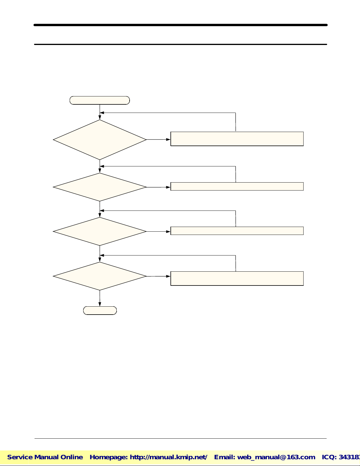
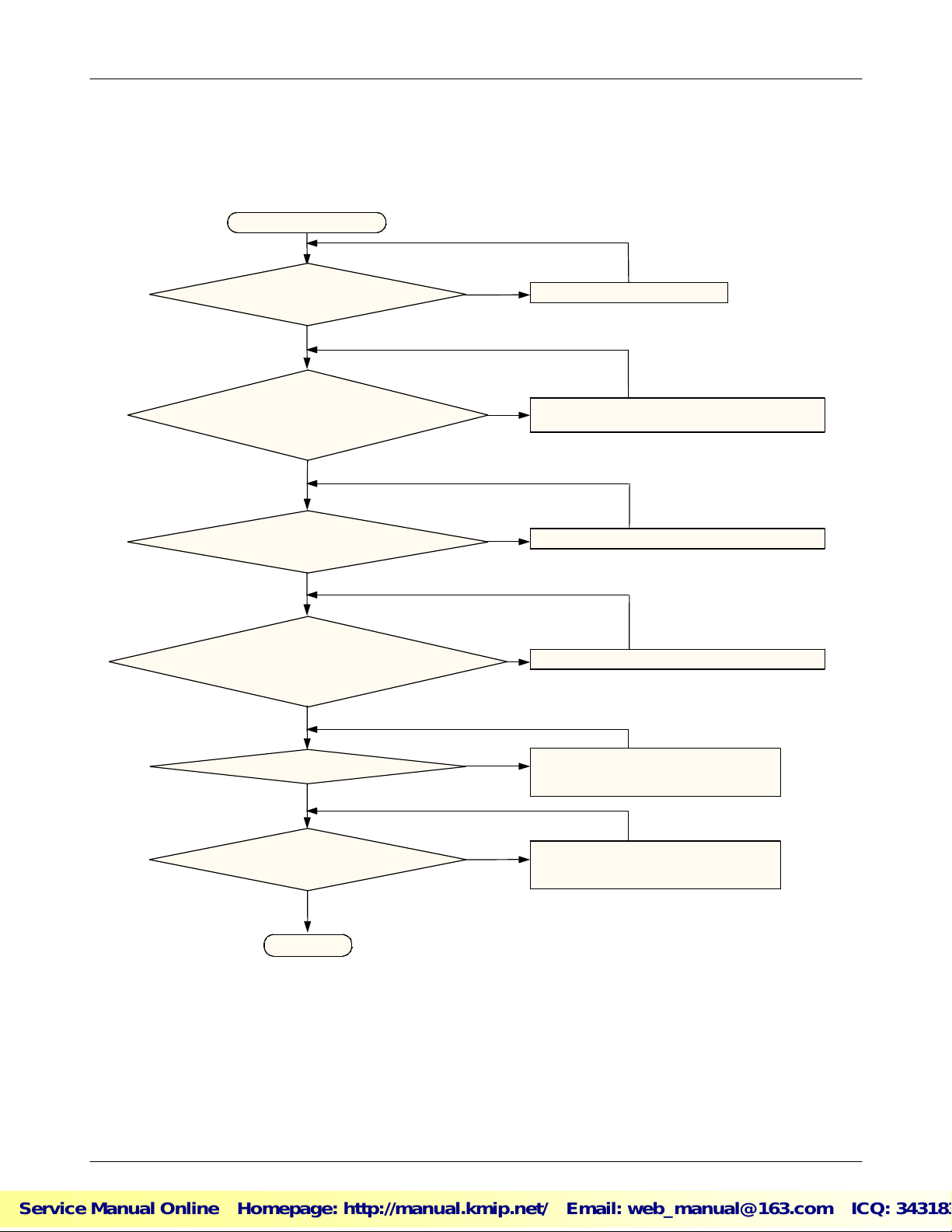
1-1. No Power
Press PWR button
"H" level
outputted from
Q307 Pin1?
Yes
U300 Pin
2=2.8V?
Yes
U300 Pin
1=2.8V?
Yes
R346
=2.8V?
Yes
No
No
No
No
Check Battery, Q503 and its neighboring
circuits
Check U300 and its neighboring circuits
Check U300 and its neighboring circuits
Check U300, U301, U302 and its
neighboring circuits
END
2-1
SAMSUNG Proprietary-Contents may change without notice
This Document can not be used without Samsung's authorization
Service Manual Online Homepage: http://manual.kmip.net/ Email: web_manual@163.com ICQ: 343183001 QQ: 35070846
SCH-X359 Flow Chart of Troubleshooting and Circuit Diagrams
Service Manual Online Homepage: http://manual.kmip.net/ Email: web_manual@163.com ICQ: 343183001 QQ: 35070846
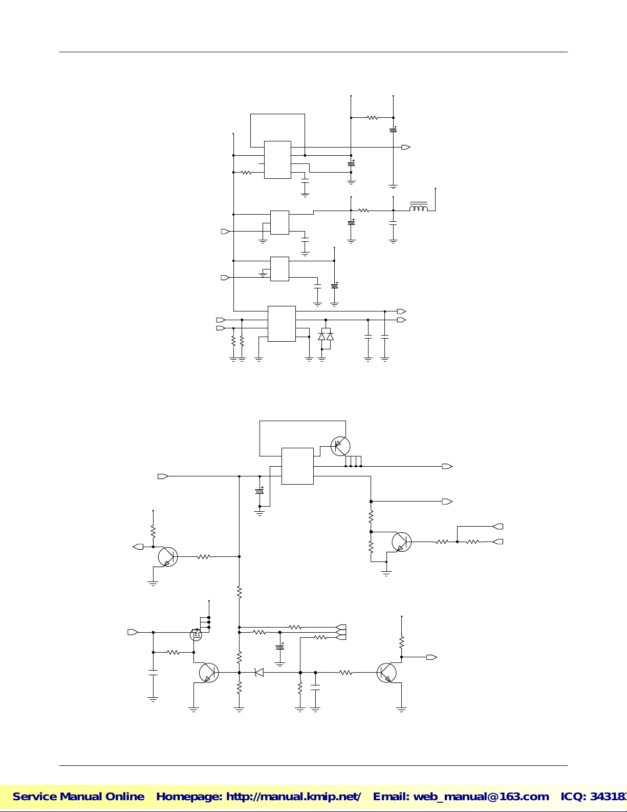
SLEEP_N
IDLE_N
BACKLIGHT_LED
MOT_CON
R323
2.8V
R300
V_IN
R303
150K
47K
R324
U300
1
8
_RESET
VDET
7
2
VOUT
VIN
3
6
GNDNC
5
4
_SHDN BYP
U301
1
IN
2
GND
3
EN
REF_BYP
U302
1
IN5OUT
2
GND
3
REF_BYP
EN
U303
1
VIN8VOUT1
2
SD1
3
SD2
GND
47K
VOUT2
OUT
ERR1
ERR2
C304
470PF
5
4
C307
1NF
4
C317
1NF
7
6
54
1
3.0VT
3
2
C306
10UF
6.3V
D300
C316
10UF
6.3V
3.0VR
C302
10UF
6.3V
R309
C318
2.8VA
0
C300
10UF
6.3V
RESIN_N
2.8VB
NC
C305
100NF
C319
1UF
330NF
2.8V
L300
V_LED
V_MOT
TA_DET_N
V_BATT
C331
100NF
TA+
2.8V
1
3
R334
12K
Q306
R347
680K
2
Q307
Q503
(Picture 1)
C332
1NF
4
3
Q304
12 56
V_BATT
ICHG
R332
R352
22K
2.7K
R335
470K
HP_PWR
PS_HOLD
ON_SW
Q305
3
2
R337
1
2.8V
R348
100K
3
1
Q308
10K
ON_SW_SENSE
R338
20K
CHG_ON
TA+
2
U305
ISENSE
1
GND
2
VCC
C326
10UF
10V
R336
47K
V_IN
6
5
2
1
S4S
3G
3
2
1
R350
22K
20K
R354
220K
R385
R346
1K
R344 1K
ZD305
C330
10UF
6.3V
R355
100K
DRIVE
VSENSE
PROG
6
5
43
R349
4.7K
(Picture 2)
2-2
SAMSUNG Proprietary-Contents may change without notice
This Document can not be used without Samsung's authorization
Service Manual Online Homepage: http://manual.kmip.net/ Email: web_manual@163.com ICQ: 343183001 QQ: 35070846
SCH-X359 Flow Chart of Troubleshooting and Circuit Diagrams
Service Manual Online Homepage: http://manual.kmip.net/ Email: web_manual@163.com ICQ: 343183001 QQ: 35070846
1-2. Abnormal initial operation (Normal +2.8V voltage source)
Press PWR button
PCM CLK applied to
U200 pin2?
Yes
TCXO CLK signal
applied outputted from
U200 pin4?
Yes
RAM_CS signal ouputted
from U201 Pin J2?
Yes
CHIP X8 CLK signal
ouputted from U202 Pin
A14?
Yes
No
Check VCTCXO Output.
No
Check U200 and its neighboring circuits.
Replace if required.
No
No
Check MSM board U202
Check MSM board U202
LED on?
Yes
Normal initial display
on LCD?
No
No
Check the LED and its
neighboring circuits.
Replace if required
Check the LCD pins and its
neighboring circuits.
Replace if required
Yes
END
2-3
SAMSUNG Proprietary-Contents may change without notice
This Document can not be used without Samsung's authorization
Service Manual Online Homepage: http://manual.kmip.net/ Email: web_manual@163.com ICQ: 343183001 QQ: 35070846
SCH-X359 Flow Chart of Troubleshooting and Circuit Diagrams
Service Manual Online Homepage: http://manual.kmip.net/ Email: web_manual@163.com ICQ: 343183001 QQ: 35070846
1
NC
2
IN
3
GND
TCXO
47PFC213
(Picture 1)
U200
R213
100K
VCC
OUT
5
4
2.8TCXO
C211
100NF
PCM_CLK
2.8V
WP
2.8V
R221
47K
RESIN_N
ROM_CS2_N
A(1:20)
A(21)
A(22)
ROM_CS1_N
RAM_CS1_N
RD_N
LB_N
A(0)
10KR222
C220
10NF
T1
T2
T3
T4
A(1)
A(2)
A(3)
A(4)
A(5)
A(6)
A(7)
A(8)
A(9)
A(10)
A(11)
A(12)
A(13)
A(14)
A(15)
A(16)
A(17)
A(18)
A(19)
A(20)
A10
B10
G2
F2
E2
D2
F3
E3
D3
C3
C7
E7
F7
C8
D8
E8
F8
D9
G9
F4
E4
D7
E6
E9
H2
J2
H3
C4
D4
C5
D5
F9
A1
B1
B5
B6
C1
F1
U201
A0
A1
A2
A3
A4
A5
A6
A7
A8
A9
A10
A11
A12
A13
A14
A15
A16
A17
A18
A19
A20
A21
CE#F1
CE1#S
OE#
LB#
UB#
WP#/ACC
RESET#
CE2#F
NC
NC
NC
NC
NC
NC
NC
NC
VCCF
VCCS
CIOF
CE2S
RY/BY#
WE#
DQ 0
DQ 1
DQ 2
DQ 3
DQ 4
DQ 5
DQ 6
DQ 7
DQ 8
DQ 9
DQ10
DQ11
DQ12
DQ13
DQ14
DQ15/A-1
VSS1
VSS2
C209
100PF
J5
J6
H9
D6
E5
C6
J3
D(0)
G4
D(1)
K4
D(2)
H5
D(3)
H6
D(4)
K7
D(5)
G7
D(6)
J8
D(7)
K3
D(8)
H4
D(9)
J4
D(10)
K5
D(11)
J7
D(12)
H7
D(13)
K8
D(14)
H8
D(15)
G3
J9
F10
NC
G1
NC
G10
NC
L1
NC
L5
NC
L6
NC
L10
NC
M1
NC
M10
NC
K6
NC
G8
NC
1
NC
2
NC
100KR209
10KR210
10KR211
LWR_N
D(0:15)
C210
100NF
(Picture 2)
2-4
SAMSUNG Proprietary-Contents may change without notice
This Document can not be used without Samsung's authorization
Service Manual Online Homepage: http://manual.kmip.net/ Email: web_manual@163.com ICQ: 343183001 QQ: 35070846
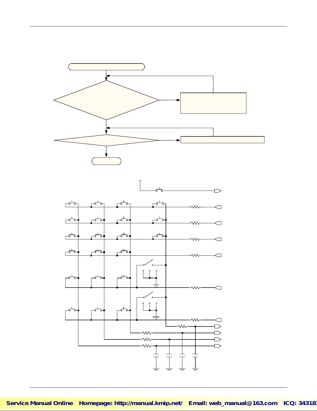
1-3. Abnormal Key Data Input
Service Manual Online Homepage: http://manual.kmip.net/ Email: web_manual@163.com ICQ: 343183001 QQ: 35070846
Check initial status
SCH-X359 Flow Chart of Troubleshooting and Circuit Diagrams
12
12
12
12
KEYPAD
12
12
Scanning signal
outputted from U100
scan 0-5, 0-3
keysense
Nomal key data input?
END
MENU
LIGHT
1
4
7
*
OVER
12
STO
12
2
2
11 2
5
12
8
KEYPAD
12
0
12
Yes
Yes
12
1
12
12
KEYPAD
12
12
LEFT
SEND
3
6
9
SH
No
R343,R345,R351,R353,R356,
Check
U100 and its neiboring
circuits
No
V_BATT
2
12
34 5
12
34 5
END_PWR
12
UNDER
12
INTERNET
12
CLR
UP
DOWN
Replace the key dome sheet
ON_SW
R343
1K
R345
1K
R351
1K
R353
1K
R356
1K
KEYSCAN(0)
KEYSCAN(1)
KEYSCAN(2)
KEYSCAN(3)
KEYSCAN(4)
1KR371
R372 1K
R373 1K
C333
100PF
C334
100PF
C335
100PF
1KR369
1KR370
C336
100PF
KEYSCAN(5)
KEYSENSE(3)
KEYSENSE(2)
KEYSENSE(1)
KEYSENSE(0)
2-5
SAMSUNG Proprietary-Contents may change without notice
This Document can not be used without Samsung's authorization
Service Manual Online Homepage: http://manual.kmip.net/ Email: web_manual@163.com ICQ: 343183001 QQ: 35070846
SCH-X359 Flow Chart of Troubleshooting and Circuit Diagrams
Service Manual Online Homepage: http://manual.kmip.net/ Email: web_manual@163.com ICQ: 343183001 QQ: 35070846
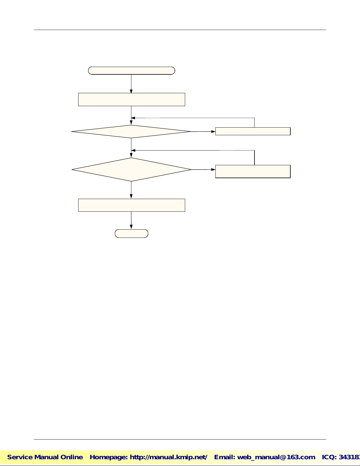
1-4. Audio
Speaker does not work
Check the connection between CN300
and LCD Module connector
Yes
U203 Pin17, 18
Yes
Check CN300
Pin31,32
Yes
Check the voltage on the speaker line
lands on LCD module
Yes
END
No
No
Check U203, U202
Check CN300 soldering
and U203 circuit
2-6
SAMSUNG Proprietary-Contents may change without notice
This Document can not be used without Samsung's authorization
 Loading...