

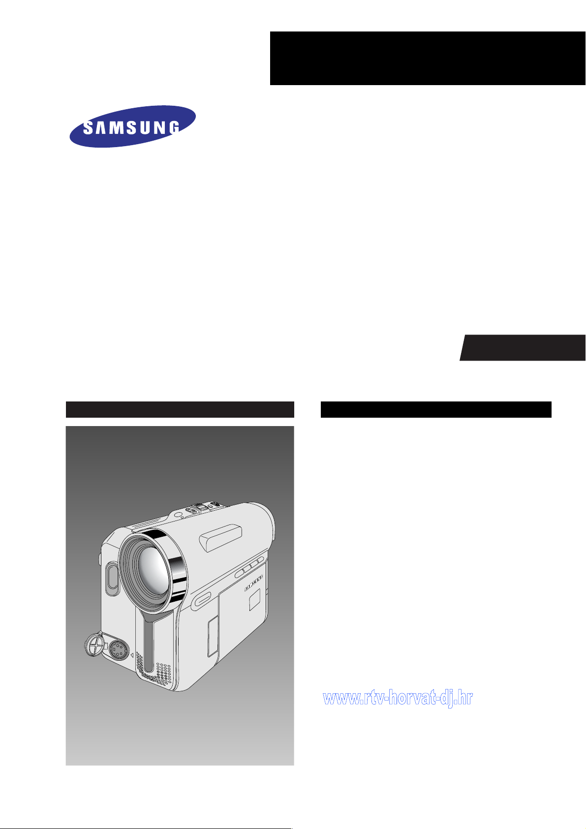
DIGITAL VIDEO CAMCORDER
Chassis : Dragon (Delta III)
BASIC : SCD353
SCD353/XAA, XAO, XAC, XTC, XAX, RCL, XAP,
TWN, GEN, ZAM, SAM, AFS, XBG
SCD352/XAA, XAO, XAC, XTC, XAX, RCL, XAP,
TWN, GEN, ZAM, SAM, AFS, XBG
SCD351/XAA, XAO, XAC, XTC, XAX, RCL, XAP,
TWN, GEN, ZAM, SAM, AFS, XBG
SERVICE
; Shooting Design DVC Leader
; Use Built-in Flash Memory
; Multi Memory Card Slot
; Direct Print System : PictBridge ™
; Power Nite Pix
; High quality MPEG4
; Still image Interpolation
; Real Wide mode (16:9)
Manual
DIGITAL VIDEO CAMCORDER Merit & Character regarding Product
1. Precautions
DEVICE
UNDER
TEST
(READING SHOULD
NOT BE ABOVE
0.5mA)
LEAKAGE
CURRENT
TESTER
EARTH
GROUND
TEST ALL
EXPOSED METER
SURFACES
ALSO TEST WITH
PLUG REVERSED
(USING AC ADAPTER
PLUG AS REQUIRED)
2-WIRE CORD
1. Be sure that all of the built-in protective devices are
replaced. Restore any missing protective shields.
2. When reinstalling the chassis and its assemblies, be
sure to restore all protective devices, including :
control knobs and compartment covers.
3. Make sure that there are no cabinet openings
through which people--particularly children
--might insert fingers and contact dangerous
voltages. Such openings include the spacing
between the picture tube and the cabinet mask,
excessively wide cabinet ventilation slots, and
improperly fitted back covers.
If the measured resistance is less than 1.0 megohm
or greater than 5.2 megohms, an abnormality exists
that must be corrected before the unit is returned
to the customer.
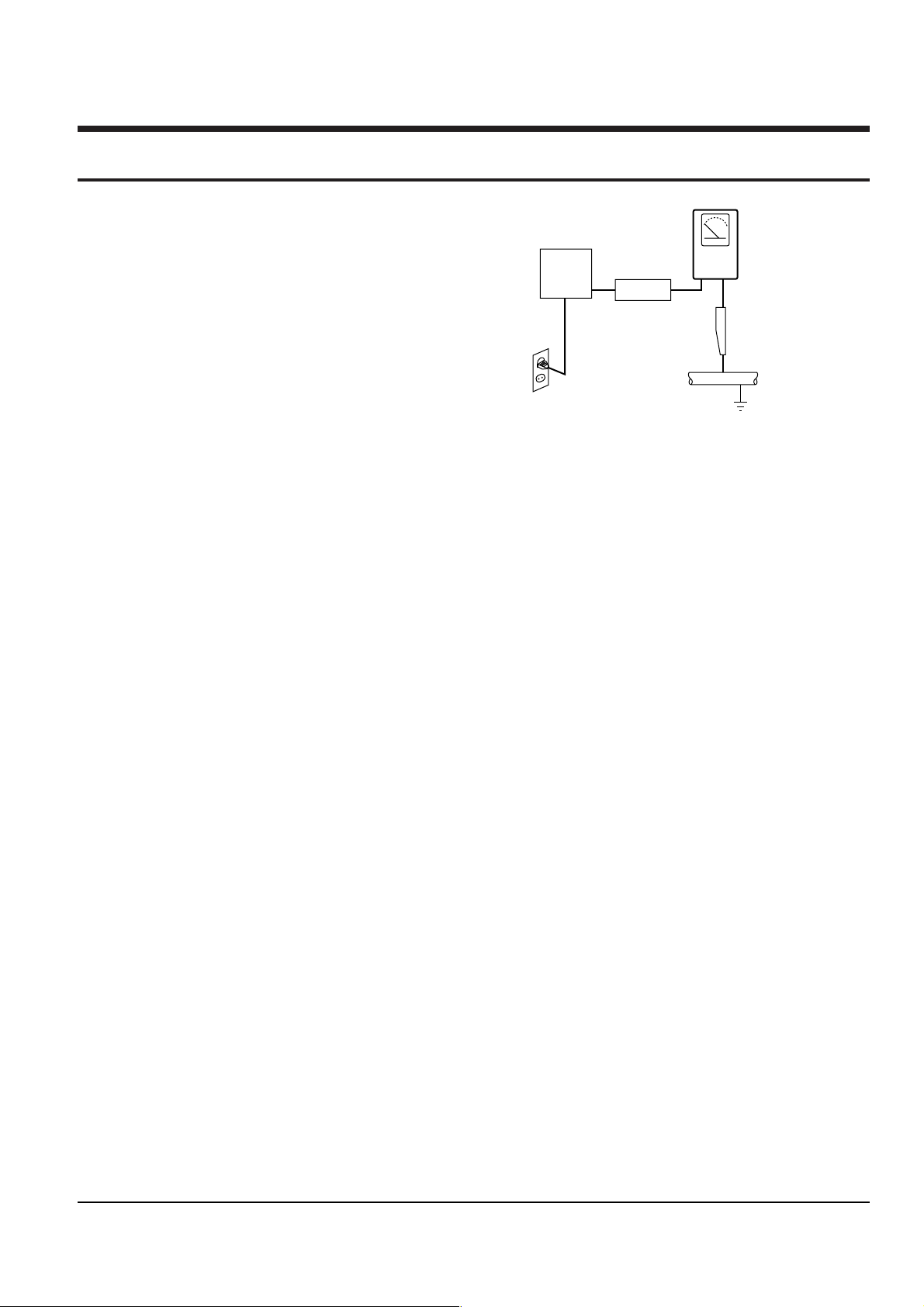
4. Leakage Current Hot Check (See Fig. 1-1) :
Warning : Do not use an isolation transformer
during this test. Use a leakage current tester or a
metering system that complies with American
National Standards Institute (ANSI C101.1,
Leakage Current for Appliances), and Underwriters
Laboratories (UL Publication UL1410, 59.7).
Fig. 1-1 AC Leakage Test
7. Antenna Cold Check :
With the unit’s AC plug disconnected from the
AC source, connect an electrical jumper across the
two AC prongs. Connect one lead of the ohmmeter
to an AC prong.
Connect the other lead to the coaxial connector.
8. High Voltage Limit :
High voltage must be measured each time
servicing is done on the B+, horizontal deflection
or high voltage circuits.
5. With the unit completely reassembled, plug the AC
line cord directly the power outlet. With the unit’s
AC switch first in the ON position and then OFF,
measure the current between a known earth
Heed the high voltage limits. These include the
X-ray protection Specifications Label, and the
Product Safety and X-ray Warning Note on the
service data schematic.
ground (metal water pipe, conduit, etc.) and all
exposed metal parts, including : antennas, handle
brackets, metal cabinets, screwheads and control
shafts. The current measured should not exceed
0.5 milliamp. Reverse the power-plug prongs in the
AC outlet and repeat the test.
9. Some semiconductor (“solid state”) devices are
easily damaged by static electricity.
Such components are called Electrostatically
Sensitive Devices (ESDs); examples include
integrated circuits and some field-effect transistors.
The following techniques will reduce the
6. X-ray Limits :
The picture tube is designed to prohibit X-ray
occurrence of component damage caused by static
electricity.
emissions. To ensure continued X-ray protection,
replace the picture tube only with one that is the
same type as the original.
10. Immediately before handling any semiconductor
components or assemblies, drain the electrostatic
charge from your body by touching a known
earth ground. Alternatively, wear a discharging
Samsung Electronics 1-1
Wrist-strap device. (Be sure to remove it prior to
applying power--this is an electric shock
precaution.)

Precautions
11. High voltage is maintained within specified limits
by close-tolerance, safety-related components and
adjustments. If the high voltage exceeds the
specified limits, check each of the special
components.
12. Design Alteration Warning :
Never alter or add to the mechanical or electrical
design of this unit. Example : Do not add
auxiliary audio or video connectors.
Such alterations might create a safety hazard.
Also, any design changes or additions will void
the manufacturer’s warranty.
13. Hot Chassis Warning :
Some TV receiver chassis are electrically
connected directly to one conductor of the AC
power cord. If an isolation transformer is not
used, these units may be safely serviced only if
the AC power plug is inserted so that the chassis
is connected to the ground side of the AC source.
To confirm that the AC power plug is inserted
correctly, do the following : Using an AC
voltmeter, measure the voltage between the
chassis and a known earth ground. If the reading
is greater than 1.0V, remove the AC power plug,
reverse its polarity and reinsert. Re-measure the
voltage between the chassis and ground.
14. Some TV chassis are designed to operate with 85
volts AC between chassis and ground, regardless
of the AC plug polarity. These units can be safely
serviced only if an isolation transformer inserted
between the receiver and the power source.
18. Picture Tube Implosion Warning :
The picture tube in this receiver employs
“integral implosion” protection. To ensure
continued implosion protection, make sure that
the replacement picture tube is the same as the
original.
19. Do not remove, install or handle the picture tube
without first putting on shatterproof goggles
equipped with side shields. Never handle the
picture tube by its neck. Some “in-line” picture
tubes are equipped with a permanently attached
deflection yoke; do not try to remove such
“permanently attached” yokes from the picture
tube.
20. Product Safety Notice :
Some electrical and mechanical parts have special
safety-related characteristics which might not be
obvious from visual inspection. These safety
features and the protection they give might be
lost if the replacement component differs from the
original--even if the replacement is rated for
higher voltage, wattage, etc.
Components that are critical for safety are
indicated in the circuit diagram by shading,
( or ).
Use replacement components that have the same
ratings, especially for flame resistance and
dielectric strength specifications. Areplacement
part that does not have the same safety
characteristics as the original might create shock,
fire or other hazards.
15. Never defeat any of the B+ voltage interlocks.
Do not apply AC power to the unit (or any of its
assemblies) unless all solid-state heat sinks are
correctly installed.
16. Always connect a test instrument’s ground lead to
the instrument chassis ground before connecting
the positive lead; always remove the instrument’s
ground lead last.
17. Observe the original lead dress, especially near
the following areas : Antenna wiring, sharp
edges, and especially the AC and high voltage
power supplies. Always inspect for pinched, outof-place, or frayed wiring. Do not change the
spacing between components and the printed
circuit board. Check the AC power cord for
damage. Make sure that leads and components
do not touch thermally hot parts.
1-2 Samsung Electronics

2. Product Specifications
2-1 Product Specification
Operation Description
System
LCD monitor/Viewfinder
Connectors
General
Video signal
Video recording system
Audio recording system
Usable cassette
Tape speed
Tape recording time
FF/REW time
Image device
Lens
Filter diameter
Size/dot number
LCD monitor Method
Viewfinder
Video output
S-video output
Audio output
DV input/output
USB output
External mic
Power source
Power source type
Power consumption
(Recording)
Operating temperature
Storage temperature
External dimension
Weight
Built-in MIC
NTSC
2 rotary heads, Helical scanning system
Rotary heads, PCM system
Digital video tape (6.35mm width): Mini DV cassette
SP: approx. 18.81mm/s LP: approx. 12.56mm/s
SP: 60 minutes (when using DVM 60), LP: 90 minutes (when using DVM 60)
Approx. 150 sec. (using DVM60 tape)
CCD / 680K (Still Image : 48K)
F1.4 20x(Optical), 900x(Digital) Electronic zoom lens
Ø30
2.5inchs 112k
TFT LCD
B/W LCD
1Vp-p (751 terminated)
Y: 1Vp-p, 751, C: 0. 286Vp-p, 751
-7.5dBs (6001 terminated)
4pin special in/out connector,
Mini-B type connector
Ø3.5 stereo
DC 8.4V, Lithium Ion Battery Pack 7.4V
Lithium Ion Battery Pack, Power supply (100V~240V) 50/60Hz
4.4W(LCD), 4.0W(Viewfinder)
0˚~40˚C (32˚F~104˚F)
-20˚C ~ 60˚C (-4˚F ~ 140˚F)
Length 90mm, Height 110mm, Width 60mm
400g (Except for Lithium Ion Battery Pack and tape)
Omni-directional stereo condenser microphone
Samsung Electronics
2-1
Product Specification
--
Acces sory Comment
-/--/ -
S-Cable / Scart Jack
Opt./Opt.Opt./Opt.
Carrying Case / Tape
T.B.DT.B.D
Battery Pack
O/XO / --/ -
Remocon / Acces sory Shoe
OO-
Analog In
O/O/OO/O/O
Multi Lang./ Batt. Check/Instant On
O/GUI/OO/GUI/OO/OSD/O
Beep Sound / Display / PB Zoom
O/O/O/-O/O/O/-
AV / S.Jack / Ext.Mic / H.phone
O/O/OO / O / O-/ -/ O
Light / Night Captur e / LSS
T.B.DT.B.D
JPEG Multi Display
T.B.DT.B.D
Continuous Shot / Im age Mix
M4/VG/30fM4/VG/30f
MPEG Clip Form at / size / F.Ratio
XGAXGA
JPEG Recording Si ze to Memory
----
Memory Card
16M32M--
Builtin Memory
Multi CardMulti CardM.S. Slot-
Memory Card Slot
MJ/QQ/15fMJ/QQ/15f
Web camera (For./size/F.rate)
M4/VG/30fM4/VG/30f
USB Stream. (For./size/F.Rate)
USB2.0USB2.0
USB
In/OutIn/Out
IEEE1394
DISDIS
Image Stabili zer
12/16b PCM12/16b PCM
Audio
BWColorBW
Viewfinder
2.5", 112K2.5", 112K
LCD
680K680K
CCD
20x / 900x20x / 900x
Zoom/Digita l Zoom
520 line520 line
Resolution
MiniDVMiniDV
Format
VM-F730D355SC-D353D351
Model cod e
NTSC (
Rsx
)NTSC(America)
Region
-
Acces sory Comment
Opt./Opt.
S-Cable / Scart Jack
Opt./Opt.
Carrying Case / Tape
T.B.D
Battery Pack
O/XX/XX/X
Remocon / Acces sory Shoe
-
Analog In
O/O/O
Multi Lang./ Batt. Check/Instant On
O/GUI/OO/OSD/OO/OSD/O
Beep Sound / Display / PB Zoom
O/O/O/-
AV / S.Jack / Ext.Mic / H.phone
O/O/O-/-/O-/-/O
Light / Night Captur e / LSS
T.B.DNoNo
JPEG Multi Display
T.B.DNoNo
Continuous Shot / Im age Mix
M4/VG/25fNoNo
MPEG Clip Form at / size / F.Ratio
XGANoNo
JPEG Recording Si ze to Memory
-
---
Memory Card
64M
---
Builtin Memory
Multi Card
M.S.NoNo
Memory Card Slot
MJ/QQ/12.5fNo
Web camera (For./size/F.rate)
M4/VG/25fNo
USB Stream. (For./size/F.Rate)
USB2.0No
USB
Out
IEEE1394
DIS
Image Stabili zer
12/16b PCM
Audio
Color
BW
Viewfinder
2.5", 112K
LCD
800K
CCD
20x / 900x
Zoom/Digita l Zoom
520 line
Resolution
MiniDV
Format
D355VP-D353D352D351
Model cod e
PAL (Europ e)
Region
O
O
O
O
O
O
O
O
O
O
O
O
O
O
O
O
O
O
O
O
O
O
O
O
O
O
O
O
O
O
O
O
O
O
OO
O
O
O
O
O
O
O
O
O
O
O
O
O
O
O
O
O
O
O
O
O
O
O
O
O
O
O
O
O
O
O
O
O
O
O
O
O
O
OO
O
O
O
O
O
O
O
O
O
O
O
O
O
O
O
O
O
O
O
O
O
O
O
O
O
O
O
O
O
O
2-2 Chassis Product Specification
2-2
Samsung Electronics
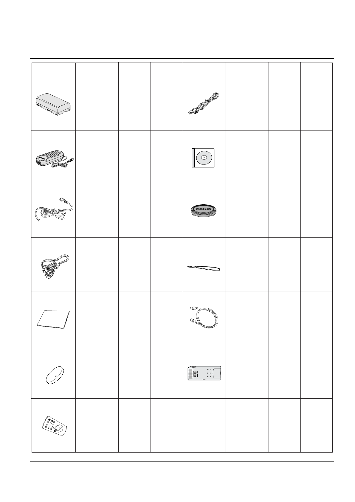
2-3 Accessories Supplied with Camcorder
(SCD354/
D355
only)
(SCD352/
D353/D354/
D355
only)
(SCD352/
D353/D354/
D355
only)
Basic
Accessories
Basic
Accessories
Basic
Accessories
Basic
Accessories
Basic
Accessories
Basic
Accessories
Basic
Accessories
Basic
Accessories
Basic
Accessories
Basic
Accessories
Basic
Accessories
Accessories
Accessories
Accessories Description Part No Remark Description Part No RemarkAccessories
1. Lithium Ion
Battery Pack
AD43-00136A
AD43-00146A
Optional
Optional
2. AC Power Adapter
(AA-E8 TYPE)
AD44-00090A
4. Audio/Video Cable
AD68-00839B
AD39-00001A
5. Instruction Book
6. Lithium Battery
(CR2025)
AD43-10130H
7. Remote Control
AD59-00085A
AD97-07354B
8. USB Cable
AD39-00073A
AD43-00128A
9.Software CD
10. Lens Cover
11.Lens Cover strap
AD72-00049A
13. Memory Stick
1109-001221
12. S-Video Cable
AC39-42001Z
3. AC
Cord
AD39-00076A
Product Specification
Samsung Electronics
2-3
3. Alignment and Adjustment
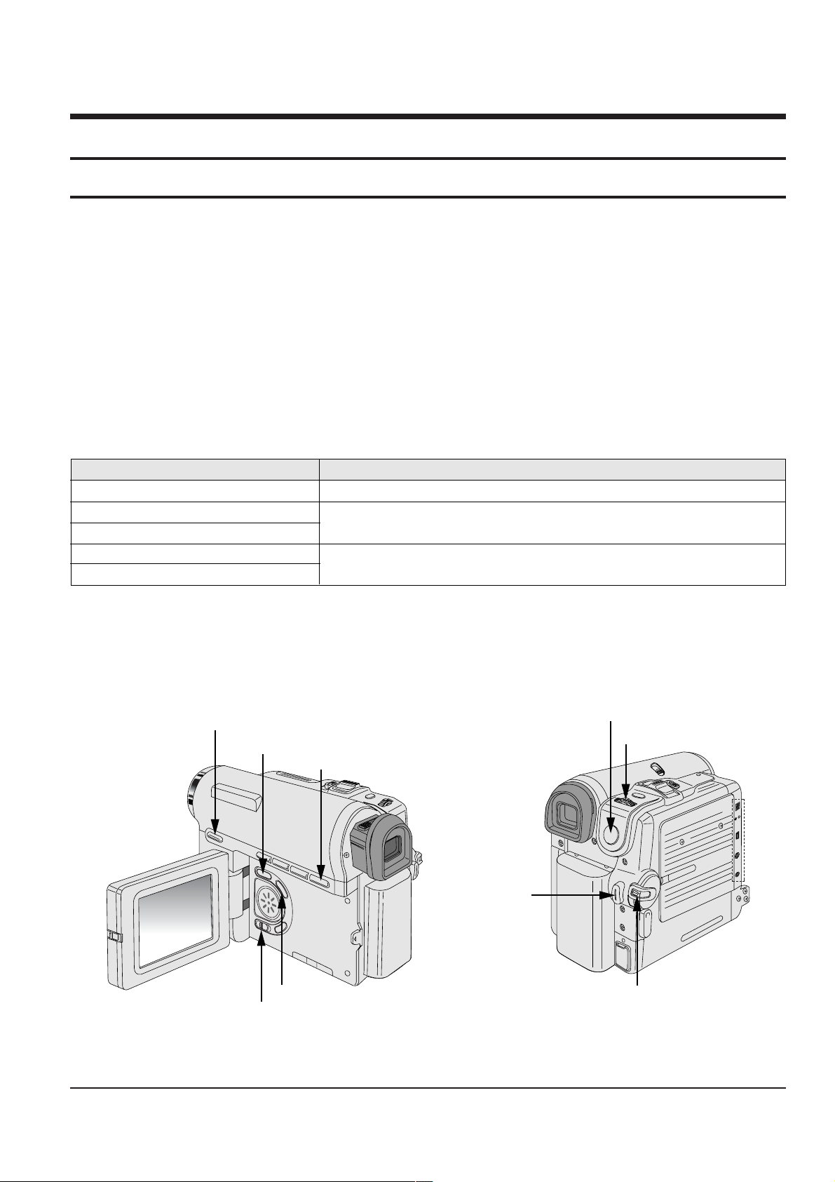
MENU Button
EASY Q Button
Start/Stop Button
MENU Selector
DISPLAY Button
Mode switch
PB ZOOM
Power switch
STOP Button
DV
USB
AV
MIC
3-1 VCR Adjustment
3-1-1 Adjustment Preparation
1) Before you start
ΠUse the buttons on the CAMCORDER when adjusting VCR.
´ When changing the adjustment item, please press the “EASY-Q” and “DISPLAY” buttons on the
CAMCORDER.
ˇ The adjustment value can be changed by moving the “MENU Selector” Left or Right.
¨ Press the “MENU Selector” to store each adjustment into EEPROM.
ˆ The OSD shows “OK” after finishing each adjustment step.
Ø In order to exit the adjustment mode, disconnect the power source.
2) Function of each buttons on the Set Key
<Table 3-1>
Buttons Description
MENU Selector push (Confirm) Stores changed value in the adjustment and auto adjustment mode.
MENU Selector Right (Data Down)
MENU Selector Left (Data Up)
EASY-Q (Mode Up)
DISPLAY (Mode Down)
Changes data in the adjustment state.
Changes mode.
3) How to get into the VCR adjust mode
[STEP 1]
ΠConnect the Power source.
´ Set the Power Switch to “PLAYER” position and Mode Switch to “TAPE” position.
Fig. 3-1
Samsung Electronics
3-1
Alignment and Adjustments
Indicates current adjustment item
Adjustment value
For Engineering Mode
Stored value
[STEP 2]
ΠPress and hold the "STOP" and "PB ZOOM" buttons on the video camera at the same time for more than
5 seconds.
´ When monitor OSD appears as shown Fig. 3-2, the adjustment mode has been activated successfully.
ˇ Move the “MENU Selector” to highlight VCR ADJ and push the “MENU Selector”.
¨ Monitor OSD shows Fig. 3-3.
Then VCR adjustment mode has been activated successfully.
[STEP 3]
In order to complete the adjustment the power must be reset.
This can be done by disconnecting and reconnecting the power source.
Fig. 3-2
Fig. 3-3
3-1-2 VCR Adjustment
Note : This is the only electronic adjustment for the VCR.
Other addresses have already been assigned data during the manufacturing process.
We don’t need any adjustment for those addresses.
<Table 3-2>
(Address)
Mode
61F SWP Position 8C Head Switching Position Adjust
Name Value Description
ΠGet into VCR ADJUST mode.
´ Move to the VCR ADJUST address “6IF”.
ˇ Play standard tape, and “Head Switching Position” will be adjusted automatically (within 5 Seconds).
3-2
Samsung Electronics

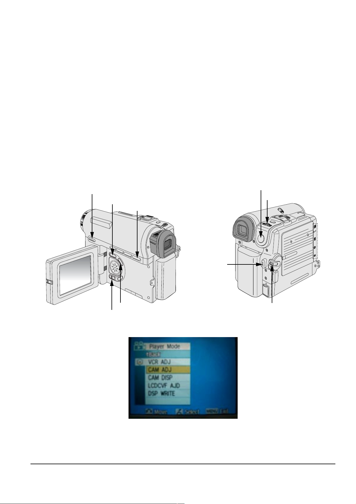
3-2 Camera Adjustment
Note : How to adjust the camera system.
1) EEPROM stores confirmed adjustment value of each adjustment step.
2) DSP (Digital Signal Process : ICM01-Main PCB) digitalizes the camera signal.
3) When changing IC505-Main PCB of EEPROM, readjust Main PCB.
While changing LCD PCB and CVF PCB- always readjust each part.
Since EEPROM stores confirmed adjustment value of each adjustment step, readjusting must be performed in order
to store the changed data.
4) Adjust the following items after changing LENS Ass’y.
ΠLens Zoom Track
´ Auto HALL
ˇ Auto IRIS
5) Adjust the following items after changing EEPROM and Camera Main PCB.
ΠLens Zoom Track
´ Zoom VR Center
ˇ Auto HALL
¨ Auto IRIS
ˆ Auto White Balance (indoor)
Ø Auto White Balance (outdoor)
Alignment and Adjustments
3-2-1 Adjustment Preparation
1) Before you start
ΠUse the buttons on the CAMCORDER when adjusting Camera.
´ When changing the adjustment item, please press the “EASY-Q” and “DISPLAY” buttons on the
CAMCORDER.
ˇ The adjustment value can be changed by moving the “MENU Selector” Left or Right.
¨ Press the “MENU Selector” to store each adjustment into EEPROM.
ˆ The OSD shows “OK” after finishing each adjustment step.
Ø In order to exit the adjustment mode, disconnect the power source.
2) Function of each buttons on the Sst Key
<Table 3-3>
Buttons Description
MENU Selector push (Confirm) Stores changed value in the adjustment and auto adjustment mode.
MENU Selector Right (Data Down)
MENU Selector Left (Data Up)
EASY-Q (Mode Up)
DISPLAY (Mode Down)
Changes data in the adjustment state.
Changes mode.
Samsung Electronics
3-3
Alignment and Adjustments
MENU Button
EASY Q Button
Start/Stop Button
MENU Selector
DISPLAY Button
Mode switch
PB ZOOM
Power switch
STOP Button
DV
USB
AV
MIC
5) How to set up the camera adjustment mode
[STEP 1]
ΠConnect the Power source.
´ Set the Power Switch to “CAM” position and Mode Switch to “TAPE” position.
[STEP 2]
ΠPress and hold the "STOP" and "PB ZOOM" buttons on the video camera at the same time for more than
5 seconds.
´ When monitor OSD appears as shown Fig. 3-5, the adjustment mode has been activated successfully.
ˇ Move the “MENU Selector” to highlight CAM ADJ and push the “MENU Selector”.
¨ Monitor OSD shows Fig. 3-6.
Then Camera adjustment mode has been activated successfully.
[STEP 3]
In order to complete the adjustment the power must be reset.
This can be done by disconnecting and reconnecting the power source.
3-4
Fig. 3-4
Fig. 3-5
Samsung Electronics
Alignment and Adjustments
Adjusted values
Stored values
3M ± 1cm
(Be sure to maintain the distance)
CCDLENS
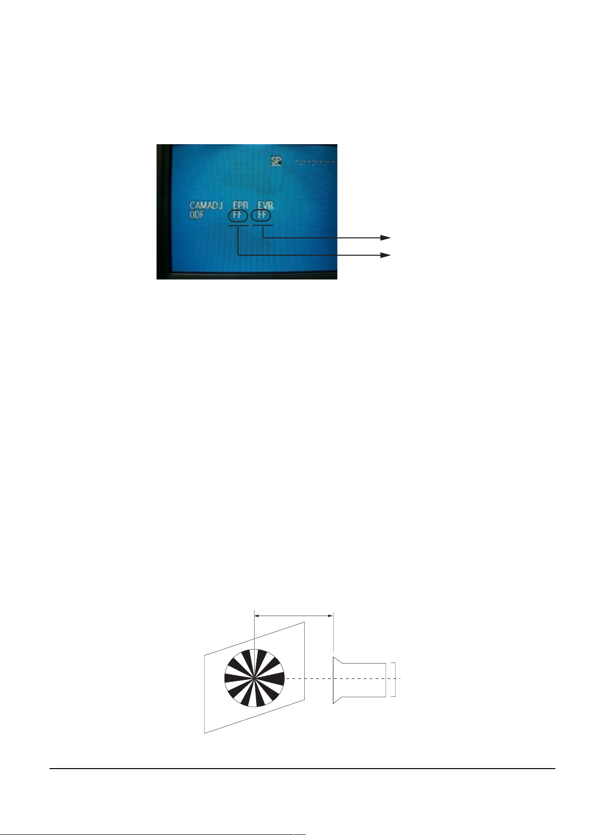
3-2-2 Camera Adjustment
Note : "XX XX" indicate the previous preset value and adjusted value.
Press the “MENU Selector” (Confirm) to store the adjusted value.
Fig. 3-6
1) EEPROM Data Initialize
Caution : These adjustments must be done when installing a new EPROM (IC105) or Main PCB.
Œ Press the “EASY-Q”(Mode Up)/”DISPLAY”(Mode Down) buttons until CAMADJ displays “0DF XX XX”.
´ Use the “MENU Selector” (Data Up/Down) until the display data for EVR is “A0”.
ˇ Press the “MENU Selector” (Confirm).
¨ The OSD shows “OK” after finishing the initalize.
2) Lens Zoom Track
Caution : For whole zoom range, it shall be in focus.
The location of a focus lens is moving depending on the location of Zoom Lens.
During adjusting, micom measures the focus location from a near distance to a long.
ΠCamera is set to E-E mode.
´ Focus chart photo.
ˇ Center the camera about 3m from a focus chart which, should be placed on a flat surfaced white or gray wall.
¨ Connect the video output terminal to a TV.
ˆ Press the “EASY-Q” (Mode Up)/”DISPLAY” (Mode Down) buttons until CAMADJ displays “0DE XX XX”.
Ø Press the “MENU Selector” to begin adjustment.
The camera must be kept still when adjusting the zoom and focus lens.
If you don’t have any chart, you can use the object which has a lot of vertical line.
The OSD shows “OK” after finishing the adjustment.
(The word “OK” is displayed for only a fraction of a second.)
Samsung Electronics
Fig. 3-7
3-5

Alignment and Adjustments
3) Zoom VR Center
ΠConnect a video output terminal to a TV.
´ Press the “EASY”(Mode Up)/”DISPLAY”(Mode Down) buttons so that OSD shows “0D6 XX XX”.
ˇ Press the “MENU Selector” (Confirm).
¨ Then Micom finds out Zoom VR center position.
Store Zoom VR center value in OB7.
4) Auto HALL
ΠConnect a video output terminal to a TV.
´ Press the “EASY-Q”(Mode Up)/”DISPLAY”(Mode Down) buttons so that OSD shows "0CD XX XX".
ˇ Press the “MENU Selector” (Confirm).
¨ Then micom finds out max. Hall value with an iris opened and min. Hall value with an iris closed.
Store max. and min. value of Hall in OAD and OAC respectively.
ˆ The OSD shows “OK” after finishing the adjustment.
(The word “OK” is displayed for only a fraction of a second.)
5) Auto IRIS Level
ΠConnect a video output terminal to a wave form monitor and a TV.
´ Press the “EASY-Q”(Mode Up)/”DISPLAY”(Mode Down) buttons so that OSD shows "0CE XX XX".
ˇ Press the “MENU Selector” (Confirm).
¨ Then micom finds out max. Hall value with an iris opened and min.
Hall value with an iris closed. Store max. and min. value of in 00BC, 00BD and 00BB respectively.
ˆ The OSD shows “OK” after finishing the adjustment.
(The word “OK” is displayed for only a fraction of a second.)
6) Auto White Balance (indoor)
Œ Camera mode & 3100˚ K gray scale chart.
´ Connect a video output terminal to a vectorscope and a TV.
ˇ Press the “EASY-Q”(Mode Up)/”DISPLAY”(Mode Down) buttons so that OSD shows "0D4 XX XX".
¨ Ensure that camera picks up image 40µs on 3100˚K gray scale chart precisely and the illumination is 1500~2000
Lux.
ˆ Press the “MENU Selector” (Confirm) to ensure that white spot on a vectorscope is moving in the middle of
screen.
Ø The OSD shows “OK” after finishing the adjustment.
(The word “OK” is displayed for only a fraction of a second.)
7) Auto White Balance (outdoor)
Œ Camera mode & 5100˚ K gray scale chart.
´ Connect a video output terminal to a vectorscope and a TV.
ˇ Press the “EASY-Q”(Mode Up)/”DISPLAY”(Mode Down) buttons so that OSD shows "0D5 XX XX".
¨ Ensure that camera picks up image 40 µs on 5100 gray scale chart (3100 gray scale chart + C16 filter) precisely
and the illumination is 1500~2000 Lux.
ˆ Press the “MENU Selector” (Confirm) to ensure that white spot on a vectorscope is moving in the middle of
screen.
Ø The OSD shows “OK” after finishing the adjustment.
(The word “OK” is displayed for only a fraction of a second.)
3-6
Samsung Electronics
3-3 Deck Adjustment
Connceted the Recorder Circuit
SWITCH C-IN
DC POWER SUPPLY
A
B
Alignment and Adjustments
3-3-1 Operation Without Housing Assembly
1) Remove the Housing Ass’y from the Deck Ass’y.
2) Connect the Mechanical Chassis to the recorder
circuit to supply voltage.
3) Set to Unload mode.
4) Press the S/W Push (Keep ON status)to start loading, and push the PLAY Key.
(Cover the Top/End sensor with black tape,
because they do not operate.)
Note : For the removal of the Housing Ass’y refer to
4-2-2 (page 4-7).
Fig. 3-8
3-3-2 Setting Mechanical Mode (Without Recorder Circuit)
1) Set the power-supply output to approx. 3V~5V.
2) Choose the polarity (depending on whether loading or unloading).
3) Supply the voltage to the Motor Loading, and set
to the desired mode.
<Table 3-4>
A B Movement of Chassis
+ - Unloading
- + Loading
Samsung Electronics
Fig. 3-9
3-7
Alignment and Adjustments
P5
P2
P4
P3
P1
P8
P6
P7
P9
PINCH ROLLER
3-3-3 Maintenance
Carry out the following periodic maintenance checks in order to fully exercise all functions, operations and tape.
After repairing, service the set as follows:
1) Cleaning of Drum Assembly
ΠGently apply lens tissue soaked in ethyl alcohol to the Drum assembly.
Clean the Upper Drum assembly while rotating it slowly counterclockwise(by hand).
Note : Do not rotate the motor by power or rotate the Upper Drum assembly clockwise.
Also, the Head tip will be damaged if the lens tissue is moved in a perpendicular direction.
Be sure to follow these instructions when cleaning the Drum Ass’y
2) Cleaning of Tape Path
ΠIn EJECT mode, clean the tape path system(from Pole Tension P1 through Pole Review P9, Pinch Roller and
Capstan Shaft) and the Lower Drum. Using the lens tissue soaked in ethyl alcohol.
Note : Make sure that no oil or grease adheres to the lens tissue.
3-8
Fig. 3-10
Samsung Electronics

3) Periodic Maintenance and Check List
2mm
OIL
When overhauling, refer to the following table.
Alignment and Adjustments
<Table 3-5>
Maintenance checks
Hours of use (H)
500 1000 1500 2000 2500 3000 3500 4000 4500 5000
system
D
R
V
N
G
Perform-
Tape
path
I
I
ance
Cleaning of tape path O O O O O O O O O O
Cleaning and degaussing of drum ass’y
S
Y
S
T
E
M
Capstan Shaft 66666
Gear Capstan 66666
Gear Pully Shaft 66666
Belt Timing ŮŮŮŮŮ
Motor Loading ŮŮŮŮŮ
OOOOOOOOOO
Abnormal Noise ŮŮŮŮŮŮŮŮŮ
Back Tension ŮŮŮŮŮ
Confirmation
Brake System ŮŮŮŮŮ
PB, REV Torque Measurement
ŮŮŮŮŮ
O : Cleaning ¨ : Oil Ů : Confirmation
Ů When lubrication bearings, be sure to keep the oil
free of dust. (Oil contaminated with dust might
cause the bearings to wear out or seize.)
Ů A“drop”of oil is defined as the amount attached to
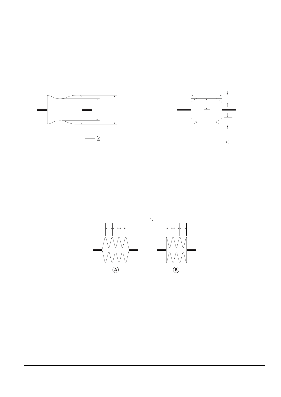
the tip of a Ø 2mm stick as shown in Fig. 3-11.
Remark
- Never let oil get on to the tape path
surface.
Samsung Electronics
Fig. 3-11
3-9

Alignment and Adjustments
1 0.5
ARM TENSION Œ
CAP ADJUST ´
"B"
"A"
3-3-4 Mechanical Check and Adjustment
3-3-4(a) Tension Regulator Adjustment
1) Disassembly
Œ For the removal of the Housing Ass’y refer to 4-2-2 (page 4-7).
2) Adjustment
ΠSet to PLAY mode (without cassette tape).
´ Check that the distance between external surface of Holder Loading and extenal diamater of Arm Tension is
1±0.5mm. (Fig. 3-12)
ˇ If necessary, proceed to step 4.
¨ If the Arm Tension Œ is located inside (or right) the position specified, adjust the Cap Adjust Œ toward
arrow “A”. (If it is located outside (or left), adjust toward arrow “B”.)
Note : Check if the Arm Tension can be moved toward arrow “C” in PB mode.
3) Reassembly
Œ For the removal of the Housing Ass’y refer to 4-2-2 (page 4-7).
3-10
Fig. 3-12
Samsung Electronics
Alignment and Adjustments
REEL DISK S TABLE
RESTING SURFACE
REEL DISK T TABLE
RESTING SURFACE
CHASSIS MAIN
b
a
3-3-4(b) Back Tension Confirmation
1) Set up the cassette-torque tape.
2) Set to CAMERA mode, push the EDIT(+) KEY and check that the torque value of Reel S is 4±1g.cm.
3) If necessary, proceed to step 4.
4) If the Tension value is Low specified, moved to toward “a”.
If the Tension value is High specified, moved to toward “b”.
Reference : After changed, insert Cassette torque tape and confirm torque value.
Fig. 3-13
3-3-4(c) PB/REV Torque check
1) Set up the cassette torque tape.
2) Set to CAMERA mode, Push the EDIT(+) button and check that the torque value of Reel T is 9.5±3.5g.cm.
3) Push the EDIT(-) button and check that the torque value of Reel S is 15±4g.cm.
4) If necessary, replace the defective Reel Disk S, T Ass’y.
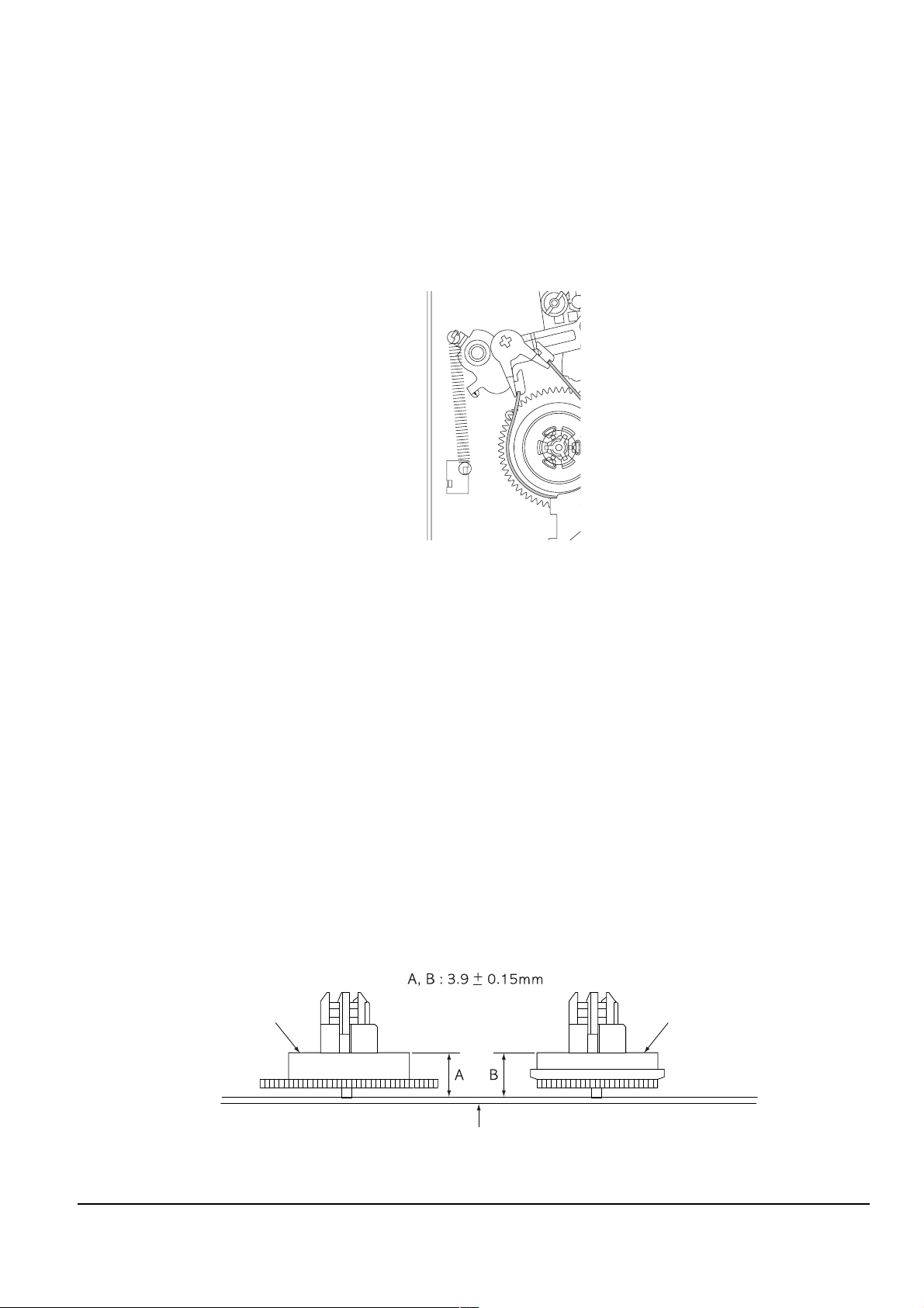
3-3-4(d) Reel Table Height Check
1) Removal
Œ For the removal of the Housing Ass’y refer to 4-2-2 (page 4-7).
´ For the removal of the Idler Ass’y refer to 4-2-3 (page 4-8).
2) Check
ΠUsing vernier calipers, check the following distances : From the upper surface of the Main Chassis to the
resting surfaces of Reel S, T table should each be 3.9±0.15mm.
3) Mounting
Œ For the removal of the Idler Ass’y refer to 4-2-3 (page 4-8).
´ For the removal of the Housing Ass’y refer to 4-2-2 (page 4-7).
Samsung Electronics
Fig. 3-14
3-11
Alignment and Adjustments
P1
P2
P3
P4
P5
P7
P6
P8
P9
A
B
C
INLET OUTLET
NORMAL
DEFECT AT INLET
DEFECT AT OUTLET
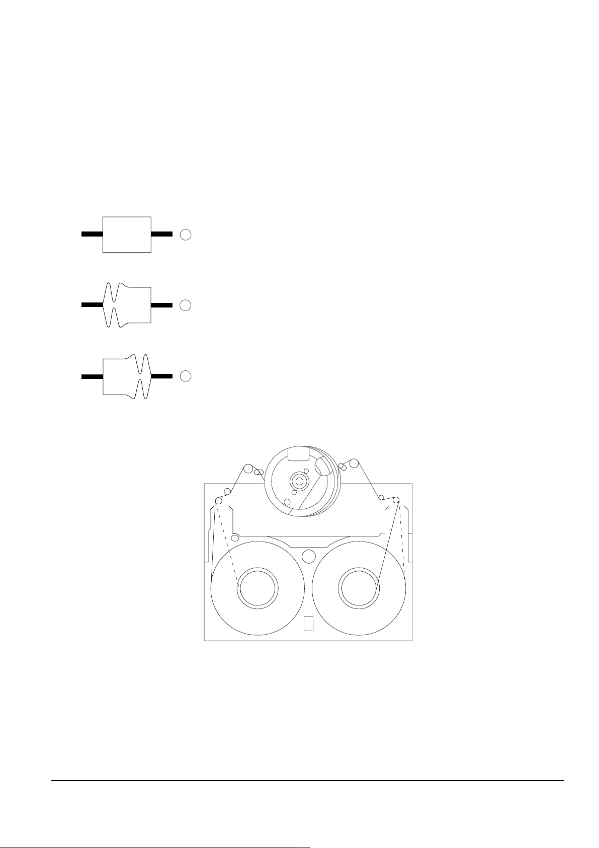
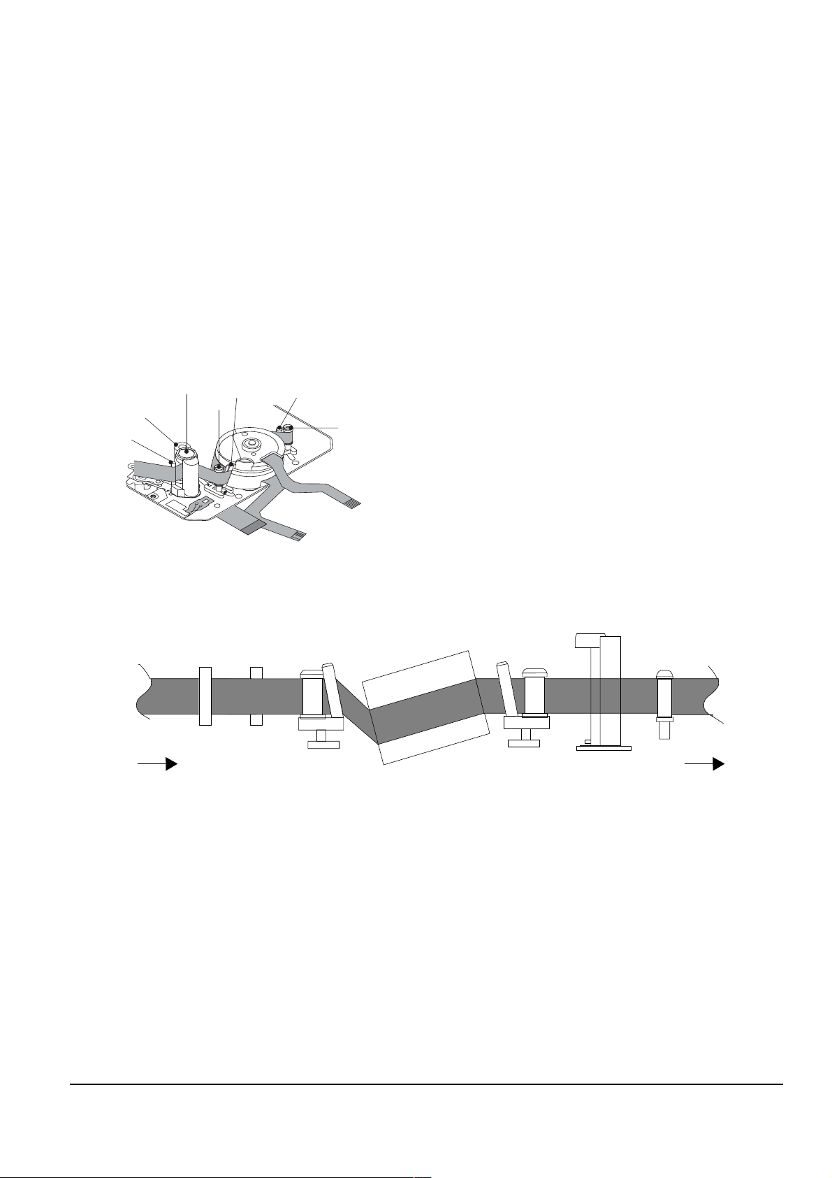
3-3-5 Tape Path Adjustment
3-3-5(a) Preparation for Adjustment
ΠClean the tape running surface (Poles, Drum, Capstan Shaft, Pinch Roller).
´ Observe the PB RF signal and Head Switching Pulse on an oscilloscope.
ˇ Play back the alignment tape.
¨ Check that the waveform of the RF signal is flat at both inlet and outlet(A in Fig. 3-15).
If not flat (B or C in Fig. 3-15), do adjustments 3-3-5(b) through 3-3-5(d).
Fig. 3-15
Fig. 3-16
3-12
Samsung Electronics
3-3-5(b) Tracking adjustment
P9
P8
P7
P6
P4
P3
MOTOR CAPSTAN
(DEFECTIVE) (CORRECT)
ΠPlay Back the alignment tape.
´ Turn P3 to flatten the waveform at the inlet.
ˇ Turn P7 to flatten the waveform at the outlet.
Alignment and Adjustments
Fig. 3-17
3-3-5(c) Take Up Path Adjustment
ΠPlay back the alignment tape, and confirm that the tape is not twisted between the Guide Roller T and
Capstan. (Fig. 3-17)
´ Set to REV mode and observe the outlet waveform of PB RF signal. (Fig. 3-18)
NOTE : If the outlet waveform is out-of-spec, replace the Arm Review or the Arm Pinch Ass’y,
and redo steps 1 and 2.
Fig. 3-18
Samsung Electronics
3-13
Alignment and Adjustments
Emin Emax
Emax
Emin
80(%)
A
A
C
C
C
1
8
abc a
abc
bc
3-3-5(d) Check After Adjustment
1) Tracking Check
ΠPlayback the alignment tape.
´ Confirm that the minimum amplitude value(E min.)is 80% of the maximum value(E max.) or larger.
(Fig. 3-19)
ˇ Confirm that no large fluctuation occur on the waveform. (Fig. 3-20)
Fig. 3-19
2) CUE and REV Check
ΠPlayback the alignment tape, and set to REV mode.
Confirm that the waveform peaks have a uniform Pitch. (Fig. 3-21 A)
If the track pitch is not uniform, do section 3-3-5(b) (Tracking adjustment).
´ Set to CUE mode.
Confirm that the waveform peaks still have a uniform pitch. (Fig. 3-21 B)
If the track pitch is not uniform, do section 3-3-5(b) (Tracking Adjustment).
Fig. 3-21
Fig. 3-20
3-14
Samsung Electronics
Alignment and Adjustments
P9
P8
P7
P6
P4
P3
MOTOR CAPSTAN
P1 P2 P3 P4 P6 P7 P9
FROM THE S REEL
TO THE T REEL
3) Rise Time Check
ΠPlayback the alignment tape.
´ Set to playback mode, and confirm that the waveform of PB RF signal rises flat within 3 seconds.
Also confirm that the tape is not twisted or curled around the Pinch Roller. (Fig. 3-23)
ˇ Run the tape in CUE/REV and FF/REW modes, then playback.
Confirm the waveform of PB RF signal rises flat within 3 seconds. Also confirm that the tape is not twisted or
curled around the Pinch Roller.
¨ Repeat steps 2. and 3.
4) Tape Path Check
ΠIn CUE and REV modes, check that the tape is not curled around the P3, P7 upper flange and P9
upper/Lower flanges.
Fig. 3-22
Fig. 3-23
Samsung Electronics
3-15
4. Disassembly and Reassembly
ΠREMOVE 3 SCREWS
(M 1.7 X 4 BLK)
ΠREMOVE 2 SCREWS
(M1.7 X 4 BLK)
´ REMOVE
2 SCREWS
(M1.7 X 4 BLK)
ˇ REMOVE 1 SCREW
(M1.7 X 5 WHT)
Caution : Please indicate that the connector
must be detached before separating
the Front Assembly
4-1 Cabinet and PCB
4-1-1 Ass’y Zoom Removal
4-1-2 Ass’y Front Removal
Fig. 4-1 Ass’y Zoom Removal
Samsung Electronics 4-1
Fig. 4-2 Ass’y Front Removal
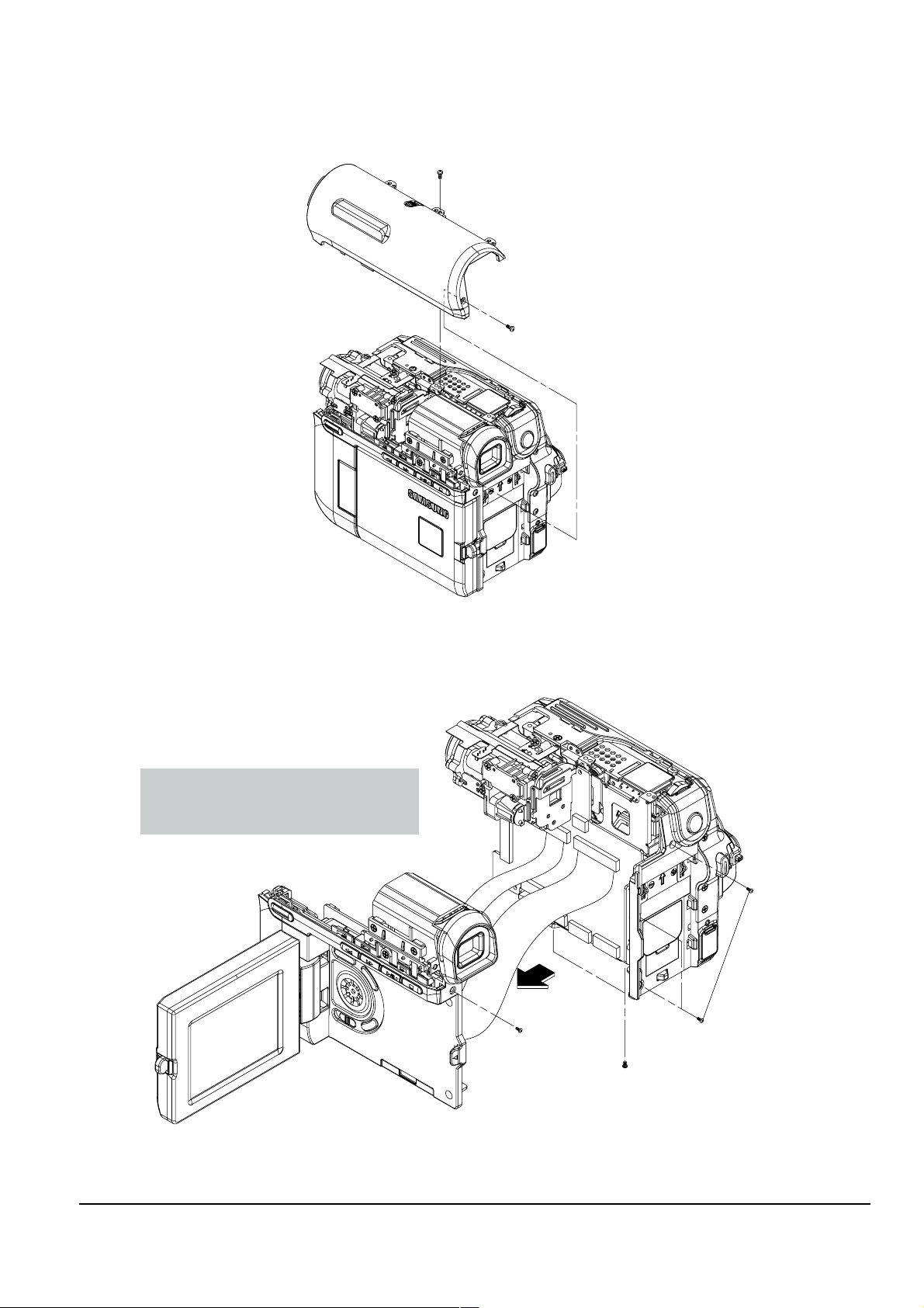
Disassembly and Reassembly
ΠREMOVE 1 SCREW
(M1.7 X 4 BLK)
´ REMOVE 1 SCREW
(M1.7 X 5 WHT)
ΠREMOVE 3 SCREWS
(M1.7 X 4 BLK)
´ REMOVE 2 SCREWS
(M1.7 X 4 BLK)
ˇ REMOVE 1 SCREW
(M1.7 X 5 WHT)
Caution : Please indicate that the connectors
must be detached before separating
the Left Assembly
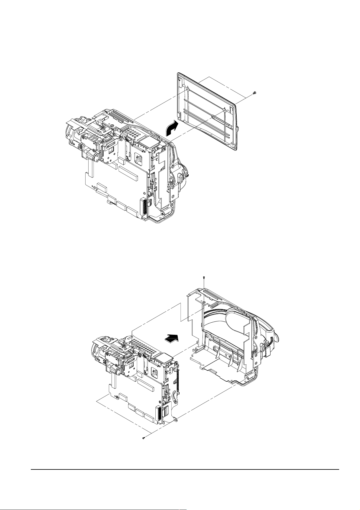
4-1-3 Ass’y Top Removal
4-1-4 Ass’y Left Removal
Fig. 4-3 Ass’y Top Removal
4-2
Fig. 4-4 Ass’y Left Removal
Samsung Electronics

4-1-5 Ass’y LCD & EVF/CVF Removal
ΠREMOVE 3 SCREWS
(T1.7 X 4 BLK)
´ REMOVE 1 SCREW
(M1.7 X 5 WHT)
ˇ REMOVE 4 SCREWS
(T2 X 5 BLK)
¨ REMOVE 2 SCREWS
(M1.7 X 3 WHT)
Caution : Please indicate that there is a
connector on the View-Finder
that must be detached
Caution : Please indicate that this connector
must be detached before separating
the LCD Assembly
ΠREMOVE 4 SCREWS
(M1.7 X 4 BLK)
Caution : The Rear Assembly is connected to the
Main PCB. Pulling it to the left as
indicated in the illustraton can cause
the connector to break. This removal
instruction should indicate that the Rear
assembly should be pulled Forward first
in order to disconnect it from the Main PCB.
Then it can be pulled to the left
to separate it from the Main PCB
Disassembly and Reassembly
4-1-6 Ass’y Rear Removal
Fig. 4-5 Ass’y LCD & EVF/CVF Removal
Fig. 4-6 Ass’y Rear Removal
4-3Samsung Electronics
Disassembly and Reassembly
ΠREMOVE 2 SCREWS
(M1.4 X 3 BLK)
ΠREMOVE 2 SCREWS
(M1.7 X 4 BLK)
´ REMOVE 2 SCREWS
(T1.7 X 4 BLK)
4-1-7 Ass’y Cover Housing Removal
4-1-8 Ass’y Right Removal
Fig. 4-7 Ass’y Cover Housing Removal
4-4
Fig. 4-8 Ass’y Right Removal
Samsung Electronics
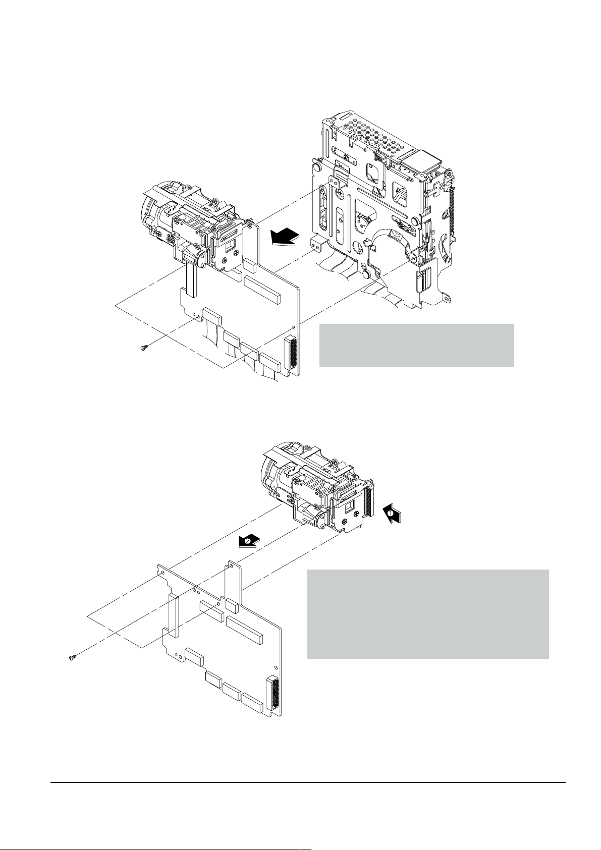
4-1-9 Ass’y Deck Removal
ΠREMOVE 3 SCREWS
(M1.7 X 2.5 BLK)
Caution : Please indicate that these connectors
must be detached before separating
the Deck Assembly from the MAIN PCB.
ΠREMOVE 3 SCREWS
(M1.7 X 2.5 BLK)
Caution : The Lens Assembly is connected to the Main PCB.
Pulling it to the left as indicated in the illustration
can cause the connector to break. This removal
instruction should indicate that the Lens assembly
should be pulled Forward first in order to disconnect
it from the Main PCB. Then it can be pulled to the
left to separate it from the Main PCB.
Disassembly and Reassembly
4-1-10 Ass’y Main PCB Removal
Fig. 4-9 Ass’y Deck Removal
Fig. 4-10 Ass’y Main PCB Removal
4-5Samsung Electronics
Disassembly and Reassembly
DC POWER SUPPLY
A
B
4-2 Deck
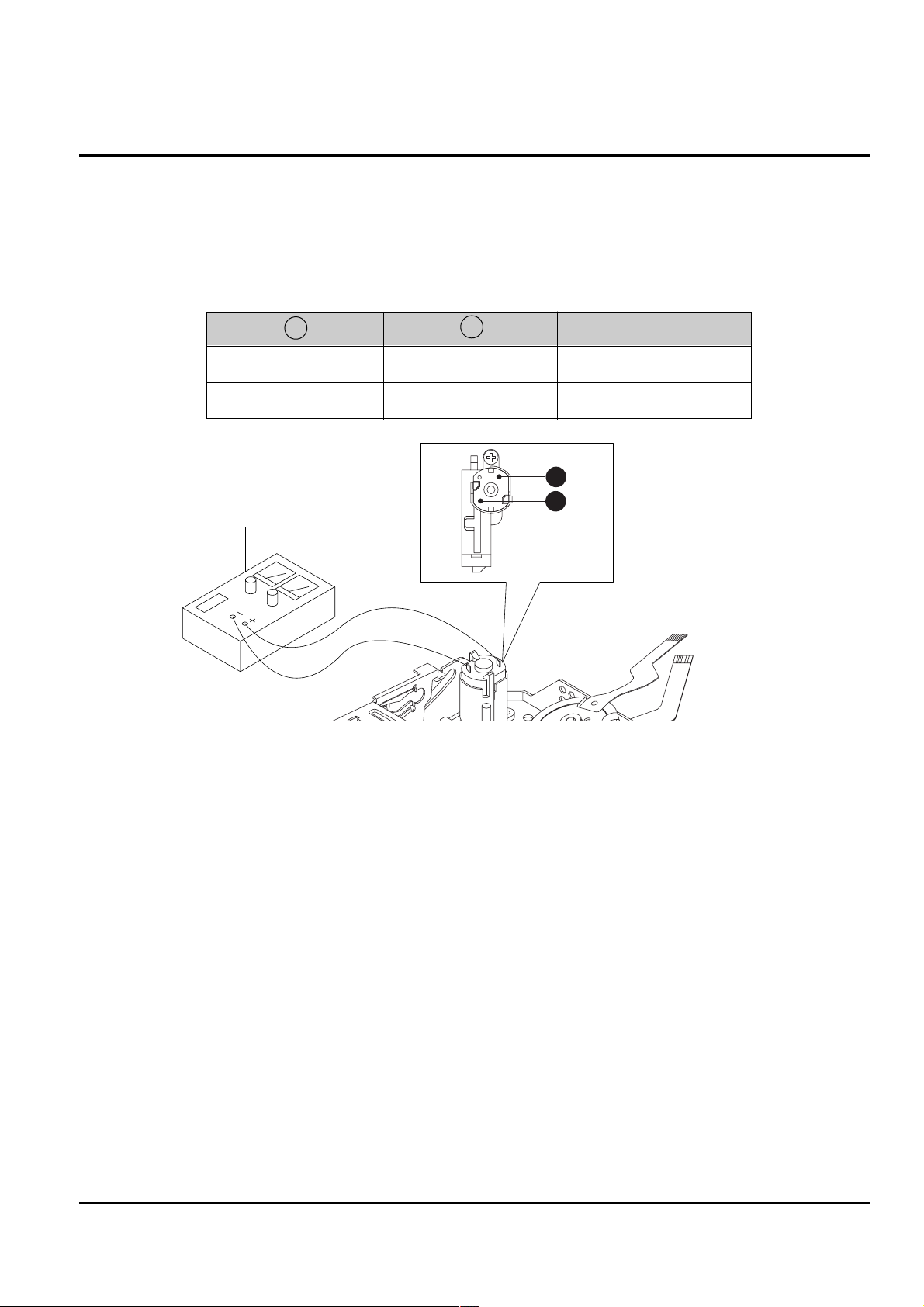
4-2-1 How to Load and Unload (Setting the Mechanical Modes)
1) Set the power-supply output to approximately 3V~5V, and connect it to the Motor Loading(= Loading Motor).
2) Choose the polarity depending on whether loading or unloading. (See Table 4-1)
3) Supply the voltage to the Motor Loading(= Loading Motor).
<Table 4-1>
AB
+
_
Fig. 4-11 Loading and Unloading
_
+ Loading
Movement of Chassis
Unloading
4-6
Samsung Electronics
4-2-2 Housing Ass’y
3
HOUSING LOCK L ´
ˇ HOUSING LOCK R
ΠLEVER LOCK
¨ LEVER HOUSING
ˆ SHAPE OF PIN
Ø CAM PART
∏ CAM PART
HOUSING ASS'Y ”
<DETAIL A>
"A"
Disassembly and Reassembly
4-2-2(a) Disassembly
Note : Do disassembly and reassembly in the
unloading mode.
1) Push the Lever(see arrow “A”, Detail A) turn the
Lever Lock Œ and open the Housing Ass’y ”.
2) Separate the Hook of Housing Lock L ´ and
Housing Lock R ˇ and then lift it.
3) Separate the Shape of Pin L and R ˆ from Cam
Parts Ø, ∏ of Main Chassis and then lift the
Housing Ass’y ”.
4-2-2(b) Reassembly
1) Mount the Shape of Pin L and R ˆ to Cam Parts Ø,
∏ of Main Chassis.
2) Mount Housing Lock L ´, R ˇ to right and left ,
and then locked.
Fig. 4-12 Housing Ass’y
4-7Samsung Electronics
Disassembly and Reassembly
"A"
2
ΠCOVER REEL ASS'Y
´ IDLER ASS'Y
4-2-3 Cover Reel Ass’y, Idler Ass’y
4-2-3(a) Disassembly
1) Lift the Cover Reel Ass’y Œ (See arrow “A”).
2) Then lift the Idler Ass’y ´.
4-2-3(b) Reassembly
1) Fit the Idler Ass’y ´ into the Pin.
2) Mount the Cover Reel Ass’y Œ to the Main Chassis
is groove in the oposite direction of arrow “A”.
4-8
Fig. 4-13 Cover Reel Ass’y, Idler Ass’y
Samsung Electronics
4-2-4 Reel Disk T, Brake T, Lever Eject
4
6
BRAKE T ´
ˇ LEVER EJECT
SHAPE OF PIN ˆ
Ø PIN
ΠREEL DISK T
¨ SHAPE OF PIN
Disassembly and Reassembly
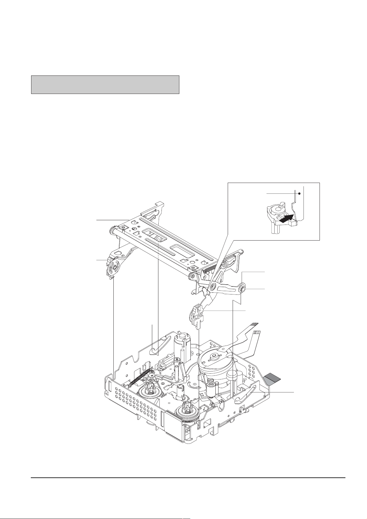
4-2-4(a) Disassembly
Note 1 : When disassembling, take care not to deform
the part. Do not stain the post.
1) Lift up the Brake T ´.
2) Lift up the Reel Disk T Œ.
3) Separate the Lever Eject’s hook from the Main
Chassis, and then Lift up the Lever Eject ˇ.
4-2-4(b) Reassembly
1) Insert the Lever Eject ˇ into the shape of pin ¨,
and then lock the Lever Eject’s hook Eliminate
this step.
2) Mount the Reel Disk T Œ to the pin Ø.
3) Insert the Brake T ´ into the shape of pin ˆ.
Fig. 4-14 Reel Disk T, Brake T, Lever Eject
4-9Samsung Electronics

Disassembly and Reassembly
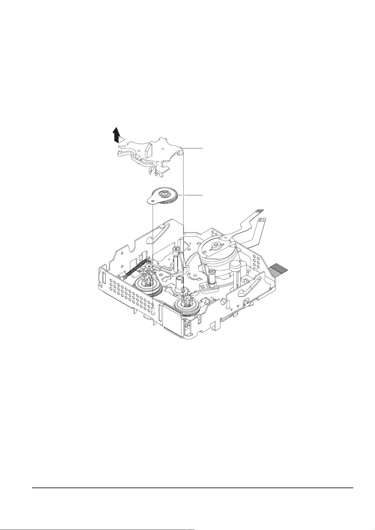
4
"A"
3
SPRING TENSION (=TENSION SPRING) Œ
ARM TENSION (=TENSION ARM) HOOK ∏
PIN Ø
MAIN CHASSIS HOOK ´
¨ ARM TENSION (=TENSION ARM) ASS'Y
ˆ REEL DISK S
ˇ WASHER SLIT
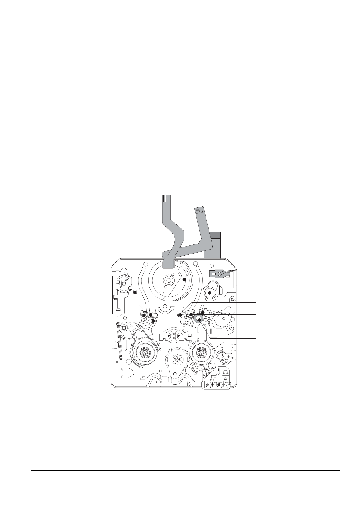
4-2-5 Arm Tension (=Tension Arm) Ass’y, Reel Disk S
4-2-5(a) Disassembly
Note 1 : When disassembling, take care not to deform
any part. Do not stain the post.
1) Separate the Spring Tension (=Tension Spring)Œ
form Hook of Main Chassis.
2) Remove the Washer Slit ˇ, and then lift up the Arm
Tension (=Tension Arm) ¨.
3) Lift up the Reel Disk S ˆ.
4-2-5(b) Reassembly
1) Mount the Reel Disk S ˆ.
2) Push the Arm Tension (=Tension Arm) Ass’y ¨
in the direction “A”, and then insert into the Pin Ø.
3) Insert the Washer Slit ˇ, and then attach the Spring
Tension (=Tension Spring) Πto Main Chassis Hook
´ and Arm Tension Hook ∏.
Note 1 : When reassembling or disassembling,
position of Spring Tension (=Tension
Spring) Πis same.
Note 2 : When inspecting the motion, Forward and
Reverse Tensions must be inspected.
Note 3 : When reassembling, confirm that the bending
of the Arm Tension (=Tension Arm) is
inserted into the Guide Cam.
Fig. 4-15 Arm Tension (=Tension Arm) Ass’y, Reel Disk S
4-10
Samsung Electronics

4-2-6 Drum
7
5
4
2
1
Ø HEAD TIP
DRUM ˇ
¨ 1 BENDING
∏ PUTTING PLACE OF DRUM
ˆ 1 HOLE
´ SPRING PLATE
Π3 SCREWS
Disassembly and Reassembly
4-2-6(a) Disassembly
Note 1 : Do not touch the Head tip Ø when removing
or reassembling the Drum ˇ.
Note 2 : Do not touch the path post when removing or
reassembling
1) Remove 3 Screws Œ, and then remove the Spring
Plate ´.
2) Lift up the Drum ˇ.
4-2-6(b) Reassembly
1) Mount and insert the Drum ˇ to the 1 Bending ¨
and 1 Hole ˆ.
2) Insert the Spring Plate ´, and then secure
3 Screws Œ.
Fig. 4-16 Drum
4-11Samsung Electronics

Disassembly and Reassembly
3
4
2
SOLDER POINTS
LOADING MOTOR ASS'Y ¨
ˇ 1 SCREW
ΠPINCH REVIEW ASS'Y
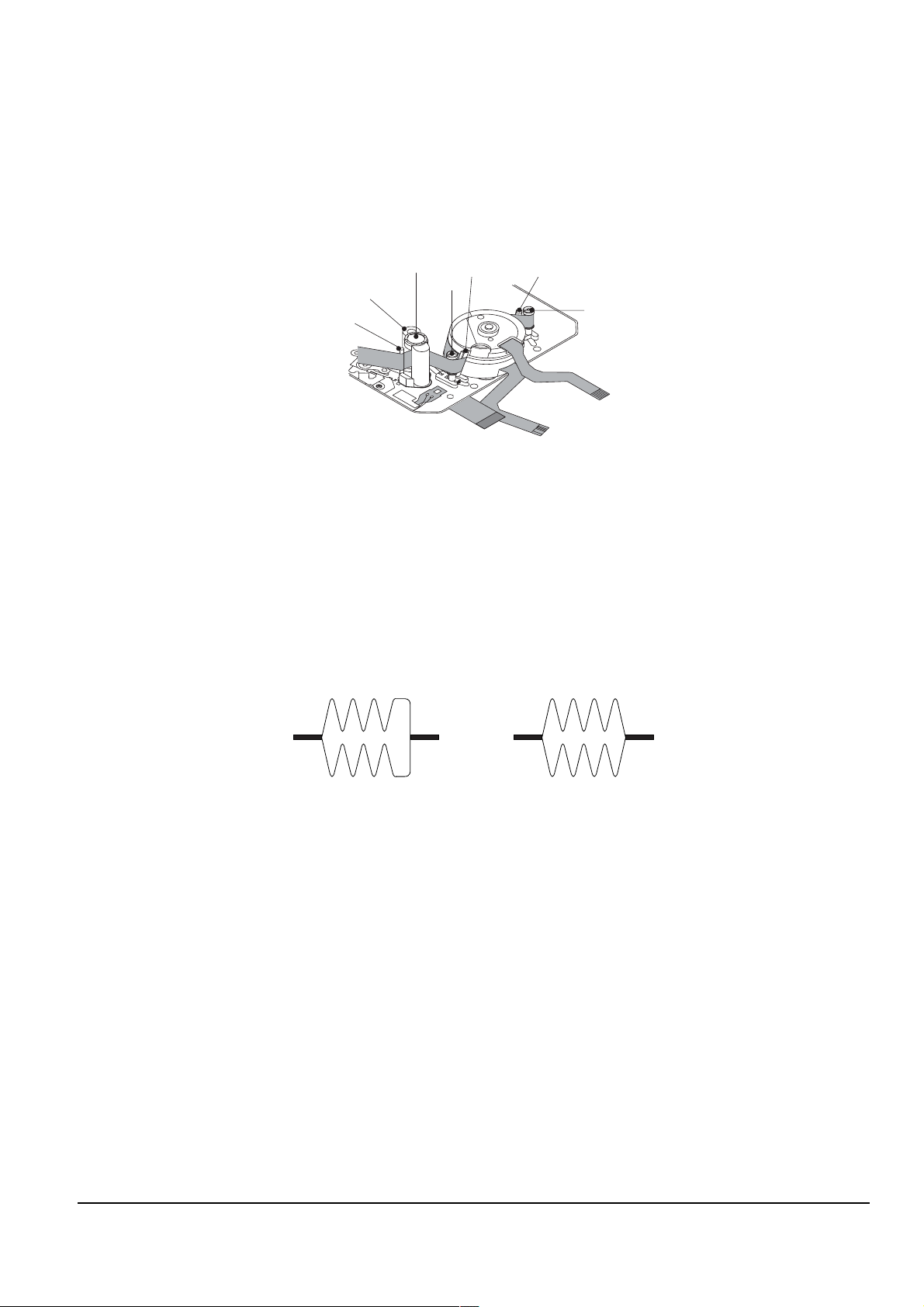
4-2-7 Loading Motor Ass’y, Pinch Review Ass’y
4-2-7(a) Disassembly
Note : When disassembling and reassembling, be
careful not to touch the Pinch Roller
and the review post.
1) In unload mode, rotate the Pinch Review Ass’y Œ
in a clockwise direction and left up the
Pinch Review Ass’y Œ.
2) De-solder the 2 points.
3) Remove the 1 screw ˇ and separate the 1 hook of
Loading Motor Ass’y ¨.
4) Lift up the Loading Motor Ass’y ¨.
4-2-7(b) Reassembly
1) Lock the one hook of Loading Motor Ass’y ¨ and
secure one screw ˇ.
2) Re-solder the 2 wires.
(+ into red wire , - into blue wire)
3) In disassembling position, insert the Pinch Review
Ass’y Œ and rotate the Pinch Review Ass’y Œ in
unload position.
4-12
Fig. 4-17 Loading Motor Ass’y, Pinch Review Ass’y
Samsung Electronics

4-2-8 Guide Roller S,T , Pole Base S,T , Gear Loading S,T Ass’y
6
2
3
GUIDE ROLLER S ˆ
ˇ POLE BASE T ASS'Y
POLE BASE S ASSY Œ
Ø GUIDE ROLLER T
GEAR LOADING S ASS'Y ´
∏ MAIN CHASSIS
¨ GEAR LOADING T ASS'Y
Disassembly and Reassembly
Note1 : When disassembling and reassembling, be
careful not to touch the Guide
Roller S ˆ and T Ø.
Note2 : When disassemblig and reassembling the
Guide Roller S ˆ and T Ø, be careful not to
deform the Gear Loading S ´ and T ¨ Ass’y.
4-2-8(a) Disassembly
1) Lift up the Pole Base S Œ(T ˇ) Ass’y form the link
of the Gear Loading S ´(T ¨) Ass’y.
2) Turn the S ˆ and T Ø Guide Rollers counter
clockwise to remove them.
3) Separate the hook of the Gear Loading S ´ and
lift down the Gear Loading S ´(T ¨) Ass’y.
4-2-8(b) Reassembly
1) Turn the S ˆ and T Ø Guide Rollers clockwise and
reassemble.
2) Replace the S ´ and T ¨ Gear Loading assemblies.
3) Fit the Pole Base S Œ(T ˇ) Ass’y in the link of the
Gear Loading S ´(T ¨) Ass’y.
Note 1 : When reassembling, confirm the assemble
point.
Note 2 : Disassembly and reassembly is done in the
Unload mode.
Note 3 : After assembling, make sure that loading and
unloading work correctly by applying 3V~5V
to the Loading Motor.
Fig. 4-18 Guide Roller S,T , Pole Base S,T , Gear Loading S,T Ass’y
4-13Samsung Electronics

Disassembly and Reassembly
Π1 SCREW
´ SLIDE MAIN
ˇ GEAR CAM MAIN
1 SCREW ¨
GEAR MODE SWITCH ˆ
GEAR CAM MAIN
ASSEMBLE POINT
(TWO ARROWS)
GEAR MODE SWITCH
4-2-9 Slide Main, Gear Cam Main, Gear Mode Switch
Note : Disassembly and reassembly must be done
with the Deck Assembly in the Unload mode.
4-2-9(a) Disassembly
1) Remove the 1 screw Œ and lift up the Slide Main ´.
2) Lift up the Gear Cam Main ˇ.
3) Remove the 1 screw ¨ and lift up the
Gear Mode Switch ˆ.
4-2-9(b) Reassembly
1) Mount the Gear Mode Switch ˆ and secure the
1 screw ¨.
2) After assemble and fit the Gear Cam Main ˇ,
Gear Mode Switch ˆ to assemble point.
3) Mount the Slide Main ´ and secure 1 screw Œ.
Note : When reassembling, confirm that pin of Slide
Main ´ is inserted into the cam of
Gear Cam Main ˇ.
Fig. 4-19 Slide Main, Gear Cam Main, Gear Mode Switch
4-14
Samsung Electronics

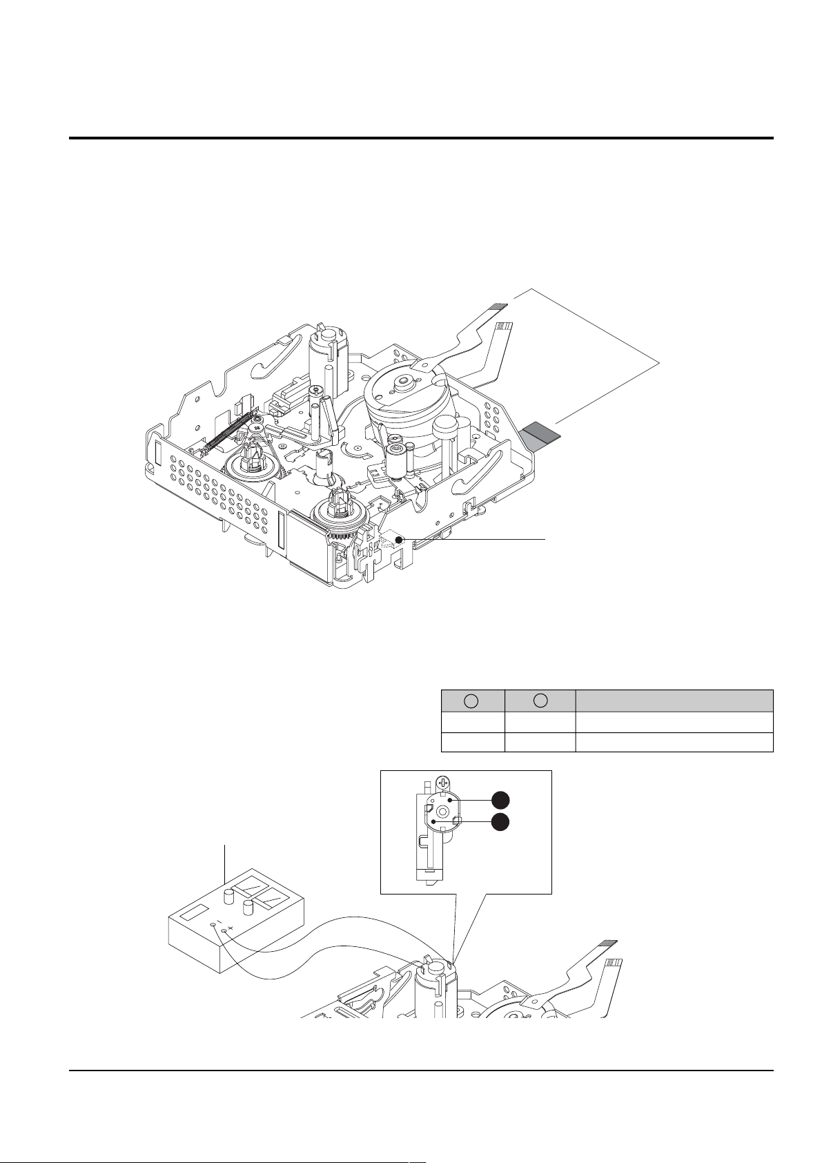
4-2-10 Cover Capstan, Capstan Motor Ass’y
2
3
4
1 SCREW Œ
´ COVER CAPSTAN
ˇ 2 SCREWS
¨ CAPSTAN MOTOR ASS'Y
Disassembly and Reassembly
Note : Be careful not to damage the gears during the
disassembly and reassembly process.
4-2-10(a) Disassembly
1) Remove the 1 Screw Œ.
2) Separe 2 hooks of Cover Capstan ´ and then lift up
the Cover Capstan ´.
3) Remove the 2 Screws ˇ, and then lift up the
Capstan Motor Ass’y ¨.
4-2-10(b) Reassembly
1) Mount the Capstan Motor Ass’y ¨ and secure the
2 Screws ˇ.
2) Lock the 2 hooks of Cover Capstan ´ and
1 Screw Œ.
Fig. 4-20 Cover Capstan, Capstan Motor Ass’y
4-15Samsung Electronics

Disassembly and Reassembly
2
3
4
LEVER REVIEW Œ
GEAR PULLEY ˆ
´ WASHER SLIT
ˇ GEAR CAPSTAN
¨ PULLEY BELT TIMING (=TIMING BELT)
4-2-11 Belt Timing (Timing Belt), Gear Capstan, Gear Pulley, Lever Review
4-2-11(a) Disassembly
1) Lift up the Lever Review Œ.
2) Remove the Washer Slit ´ and lift up the
Gear Capstan ˇ.
3) Separate the Pulley Belt Timing (=Timing Belt) ¨
and lift down the Gear Pulley ˆ.
4-2-11(b) Reassembly
1) Mount the Gear Pulley ˆ and hang the Belt
Timing (=Timing Belt) ¨ on the Gear Pulley ˆ.
2) Hang the Pulley Belt Timing ¨ on the lower gear
of the Gear Capstan ˇ, and then mount the Gear
Capstan ˇ.
3) Insert the Washer Slit ´.
4) Mount the Lever Review Œ.
Fig. 4-21 Belt Timing (=Timing Belt), Gear Capstan, Gear Pulley, Lever Review
4-16
Samsung Electronics

5. Exploded View and Parts List
Page
5-1 Ass’y Chassis - - - - - - - - - - - - - - - - - - - - - - - - - - - - - - - - - - - - - - - - - - - - 5-2
5-2 Ass’y Left (SCD353) - - - - - - - - - - - - - - - - - - - - - - - - - - - - - - - - - - - - - - - - 5-4
5-3 Ass’y Left (SCD352/SCD351)- - - - - - - - - - - - - - - - - - - - - - - - - - - - - - - - - - - 5-6
5-4 Ass’y LCD- - - - - - - - - - - - - - - - - - - - - - - - - - - - - - - - - - - - - - - - - - - - - - - 5-8
5-5 Ass’y Front (SCD353/SCD351)- - - - - - - - - - - - - - - - - - - - - - - - - - - - - - - - - - 5-10
5-6 Ass’y Front (SCD352) - - - - - - - - - - - - - - - - - - - - - - - - - - - - - - - - - - - - - - - 5-12
5-7 Ass’y Rear - - - - - - - - - - - - - - - - - - - - - - - - - - - - - - - - - - - - - - - - - - - - - - 5-14
5-8 Ass’y EVF - - - - - - - - - - - - - - - - - - - - - - - - - - - - - - - - - - - - - - - - - - - - - - - 5-15
5-9 Ass’y Zoom- - - - - - - - - - - - - - - - - - - - - - - - - - - - - - - - - - - - - - - - - - - - - - 5-16
5-10 Ass’y Case Right - - - - - - - - - - - - - - - - - - - - - - - - - - - - - - - - - - - - - - - - - 5-17
5-11 Mechanical Parts (Main Chassis) - - - - - - - - - - - - - - - - - - - - - - - - - - - - - 5-18
5-12 Mechanical Parts (Sub Chassis) - - - - - - - - - - - - - - - - - - - - - - - - - - - - - - 5-20
Notice
You can search for the updated part code through ITSELF web site.
URL; http://itself.sec.samsung.co.kr
Samsung Electronics 5-1

Exploded View and Parts List
W125
W126
C201
C607 P053
P002
W126
W125
P051
W225
P001
C050
M001
(M1.7 X L4 BLK)
(M1.7 X L4 BLK)
(M1.7 X L2.5 BLK)
(M1.7 X L2.5 BLK)
(M1.4 X L4.7 (2.5) YEL)
5-1 Ass’y Chassis
5-2 Samsung Electronics

Exploded View and Parts List
Loc. No Parts No. Description ; Specification Remark
C050 AD97-09608A ASSY-CHASSIS DECK;ASSY,DRAGON-PJ,C201 AD61-01994A BRACKET-LENS;DRAGON-PJ,SUS304 1/2H,T0.5,
C607 0605-001099 CCD;COLOR,DIP,14P,8.2x8.36x3.5mm,6
M001 AD97-09507A ASSY-DECK;ASSY,DD-10,P001 AD97-09528A ASSY-MAIN BOARD;DRAGON-PJ,SC-D353,MAIN B SCD353 Only
AD97-09528C ASSY-MAIN BOARD;DRAGON-PJ,SC-D352,MAIN B SCD352 Only
AD97-09528E ASSY-MAIN;DRAGON-PJ,SC-D351,MAIN BOARD(N SCD351 Only
P002 AD97-09533A ASSY-CCD BOARD;-,DELTA3,CCD BOARD,C
P051 AD97-08324A ASSY-LENS-ZOOM;PC,SHML,20X
P053 AD60-00053A SPACER-CCD;ALPHA_PJ,SILICON,-,-,-,BLK,0.
W125 6001-001385 SCREW-MACHINE;CH,+,M1.7,L2.5,ZPC(BLK),SW
W126 6003-001300 SCREW-TAPTITE;CH,+,B,M1.7,L4,ZPC(BLK),SW
W225 6009-001410 SCREW-SPECIAL;CH,+,-,M1.4,L4.7(2.5),ZPC(
5-3Samsung Electronics

Exploded View and Parts List
W112
P003
W112
P054
C007
C002
C208
W117
C003
C008
P004
C626
W112
C001
C623
C622
C323
C208
W112
W112
C621
C005
C640
C635
5-2 Ass’y Left (SCD353)
5-4 Samsung Electronics

Exploded View and Parts List
Loc. No Parts No. Description ; Specification Remark
C001 AD63-00709A COVER-LEFT;DRAGON-PJ,ABS,T14,W30,L58,-,C002 AD61-01977B CASE-LEFT;SC-D353,ABS 94HB,T25,W79,L99,S
C003 AD61-01694A HOLDER-TRIPOD;THETA3-PJ,PC,T1.0,W30,L14,
C005 AD63-00706B COVER-DOOR;DRAGON-PJ,PC,T1,W10,L29,-,-,?
C007 AD61-01988A HOLDER-SELECT;DRAGON-PJ,POM,T7,W8,L11,NA
C008 AD64-01322A KNOB-SELECT;DRAGON-PJ,ABS,T4,W5,L8,-,SIL
C208 AD61-12033A BRACKET-NUT;SV-D10,SECC,-,-,-,-,T0.8
C323 AD61-02069A HOLDER-DOOR MS;DRAGON-PJ,ABS,T7,W12,L32,
C621 AD61-01990A BRACKET-DOOR;DRAGON-PJ,SUS304 1/2H,T0.8,
C622 AD64-01314A BUTTON-FUNCTION A;DRAGON-PJ,ABS,W11xH10x
C623 AD64-01315A BUTTON-FUNCTION B;DRAGON-PJ,ABS,W45xH14x
C626 AD63-00716A COVER-DUMMY FUNCTION;DRAGON-PJ,ABS,T9,W1
C635 AD66-00350A SHAFT-DOOR;DRAGON-PJ,SUS,L35,0.8,-,-,C640 AD61-02005A SPRING ETC-DOOR;DRAGON-PJ,SUS,0.2,1,1.4,
P003 AD97-09524C ASSY-LEFT BOARD;DRAGON-PJ,M/S, EVF,LEFT
P004 AD97-09526A ASSY-FUNCTION BOARD;DRAGON-PJ,VP-D353,FU
P054 AD97-08377A ASSY-SPEAKER;DELTA2-PJ,SC-D103,SPEAKER
W112 6003-001453 SCREW-TAPTITE;BH,+,B,M1.7,L4,ZPC(BLK)
W117 6003-001490 SCREW-TAPTITE;PH,+,B,M1.7,L4,NI PLT,SWCH
5-5Samsung Electronics

Exploded View and Parts List
W112
P003
W112
P054
C002
C208
W117
C003
P004
C626
W112
C001
C623
C622
C208
W112
5-3 Ass’y Left (SCD352/SCD351)
5-6 Samsung Electronics

Exploded View and Parts List
Loc. No Parts No. Description ; Specification Remark
C001 AD63-00709A COVER-LEFT;DRAGON-PJ,ABS,T14,W30,L58,-,C002 AD61-01977E CASE-LEFT;SC-D352,ABS 94HB,T25,W79,L99,S SCD352 Only
AD61-01977C CASE-LEFT;SC-D351,ABS 94HB,T25,W79,L99,S SCD351 Only
C003 AD61-01694A HOLDER-TRIPOD;THETA3-PJ,PC,T1.0,W30,L14,
C208 AD61-12033A BRACKET-NUT;SV-D10,SECC,-,-,-,-,T0.8
C622 AD64-01314A BUTTON-FUNCTION A;DRAGON-PJ,ABS,W11xH10x
C623 AD64-01315A BUTTON-FUNCTION B;DRAGON-PJ,ABS,W45xH14x
C626 AD63-00716A COVER-DUMMY FUNCTION;DRAGON-PJ,ABS,T9,W1
P003 AD97-09524B ASSY-LEFT BOARD;DRAGON-PJ,NO Slot, EVF,L SCD352/351 Only
P004 AD97-09526A ASSY-FUNCTION BOARD;DRAGON-PJ,VP-D353,FU
P054 AD97-08377A ASSY-SPEAKER;DELTA2-PJ,SC-D103,SPEAKER
W112 6003-001453 SCREW-TAPTITE;BH,+,B,M1.7,L4,ZPC(BLK)
W117 6003-001490 SCREW-TAPTITE;PH,+,B,M1.7,L4,NI PLT,SWCH
5-7Samsung Electronics

Exploded View and Parts List
L010
L006
L009
L007
L008
W118
L011
W112
L004
C349
L053
L013
L001
W116
L015
L017
L016
L014
W117
W120
C208
W118
5-4 Ass’y LCD
5-8 Samsung Electronics

Exploded View and Parts List
Loc. No Parts No. Description ; Specification Remark
C208 AD61-12033A BRACKET-NUT;SV-D10,SECC,-,-,-,-,T0.8
C349 AD97-09664A ASSY-LED BL;-,DELTA3-PJ,LED BACK LIGHT
L001 AD97-09605C ASSY-LCD;ASSY,SC-D353,- SCD353 Only
AD97-09605B ASSY-LCD;ASSY,SC-D352,DRAGON-PJ SCD352 Only
AD97-09605A ASSY-LCD;ASSY,SC-D351,- SCD351 Only
L004 AD97-09599A ASSY-LCD BOARD;DRAGON-PJ,DIGITAL,LCD BOA
L006 AD61-01974C CASE-LCD TOP;SC-D353,ABS 94HB,T7,W50,L70 SCD353 Only
AD61-01974B CASE-LCD TOP;SC-D352,ABS 94HB,T7,W50,L70 SCD352 Only
AD61-01974A CASE-LCD TOP;DRAGON-PJ,ABS 94HB,T7,W50,L SCD351 Only
L007 AD64-01329A LOCKER-LCD;DRAGON-PJ,POM,NATU,-,-,T3.5,W
L008 AD63-00745A COVER-LOCK LCD;DRAGON-PJ,ABS,T2,W5,L8,-,
L009 AD61-01299A SPRING ETC-LOCK LCD;THETA-PJ,SWPB,-,-,-,
L010 AD64-01332B INLAY-MS;DRAGON-PJ,PC,T0.6,W15,L15,SIL, SCD353 Only
AD64-01332C INLAY-DV;DRAGON-PJ,PC,T0.6,W15,L15,SIL, SCD352/351 Only
L011 AD64-00808A BADGE-SAMSUNG;ALPHA_PJ,AL,T0.7,-,-,-,SIL
L013 AD61-01975A CASE-LCD BOTTOM;DRAGON-PJ,ABS 94HB,T4,W5
L014 AD63-00562A COVER-HINGE TOP 2.5;DELTA2-PJ,ABS 94V0,
L015 AD63-00563A COVER-HINGE BOTTOM 2.5;DELTA2-PJ,ABS 94
L016 AD97-08469A ASSY-HINGE;-,DELTA2-PJ,HINGE
L017 AD97-06489A ASSY-LCD FPC;.,DELTA-PJ,LCD FPC
L053 AD07-00049A LCD-PANNEL;A024CN02 V0,DELTA3-PJ,480*234
W112 6003-001453 SCREW-TAPTITE;BH,+,B,M1.7,L4,ZPC(BLK)
W116 6001-001527 SCREW-MACHINE;CH(0.3),+,M1.7,L2.0,NI PLT
W117 6003-001490 SCREW-TAPTITE;PH,+,B,M1.7,L4,NI PLT,SWCH
W118 6003-001291 SCREW-TAPTITE;CH,+,B,M1.4,L3.0,ZPC(BLK),
W118 6003-001291 SCREW-TAPTITE;CH,+,B,M1.4,L3.0,ZPC(BLK),
W120 6001-001716 SCREW-MACHINE;BH,+,M2,L4,NI PLT
5-9Samsung Electronics

Exploded View and Parts List
C210
C471
C625
C062
C031
P058
C013
W127
C037
C597
C627
W112
W127
W112
W112
C208
C034
W112
P006
5-5 Ass’y Front (SCD353/SCD351)
5-10 Samsung Electronics

Exploded View and Parts List
Loc. No Parts No. Description ; Specification Remark
C013 AD63-00713A COVER-JACK;DRAGON-PJ,ABS+URETHAN,T3,W8,L
C031 AD63-00568A SHEET-MIC;DELTA2-PJ,0Œ¡˜6˜,T0.2,W12.2,L2
C034 AD61-01976A CASE-FRONT;DRAGON-PJ,ABS 94HB,T13,W20,L8
C037 AD61-01984A HOLDER-HOOD;DRAGON-PJ,PC,T10,W34,L34,BLK
C062 AD63-00707A COVER-FRONT;DRAGON-PJ,ABS,T5,W23,L55,-,C208 AD61-12033A BRACKET-NUT;SV-D10,SECC,-,-,-,-,T0.8
C210 AD61-01993A BRACKET-GRIP FRONT;DRAGON-PJ,SUS304 1/2H
C471 AD63-00705A COVER-S JACK;DRAGON-PJ,URETHAN,T3,W14,L1
C597 AD63-00711A COVER-TOP;DRAGON-PJ,ABS,T34,W38,L102,-,C625 AD63-00714A COVER-DUMMY FRONT;DRAGON-PJ,ABS 94HB,T23 SCD353 Only
AD63-00714B COVER-DUMMY FRONT;DRAGON-PJ,ABS 94HB,T23 SCD351 Only
C627 AD63-00719A COVER-DUMMY TOP;DRAGON-PJ,PC,T11,W11,L8,
P006 AD97-09525F ASSY-JACK BOARD;DRAGON-PJ,USB,JACK BOARD SCD353 Only
AD97-09525B ASSY-JACK BOARD;DRAGON-PJ,ALL(X),JACK BO SCD351 Only
P058 AD97-08597A ASSY-UNIT MIC;-,THETA2-PJ,UNIT MIC
W112 6003-001453 SCREW-TAPTITE;BH,+,B,M1.7,L4,ZPC(BLK)
W127 6003-001292 SCREW-TAPTITE;CH(0.3),+,B,M1.7,L3,ZPC(BL
5-11Samsung Electronics

Exploded View and Parts List
C210
C471
C625
C062
C031
P058
C013
W127
C037
C597
C053
C054
C658
W127
C627
W112
W127
W112
W112
C208
C034
W112
P006
5-6 Ass’y Front (SCD352)
5-12 Samsung Electronics

Exploded View and Parts List
Loc. No Parts No. Description ; Specification Remark
C013 AD63-00713A COVER-JACK;DRAGON-PJ,ABS+URETHAN,T3,W8,L
C031 AD63-00568A SHEET-MIC;DELTA2-PJ,0Œ¡˜6˜,T0.2,W12.2,L2
C034 AD61-01976A CASE-FRONT;DRAGON-PJ,ABS 94HB,T13,W20,L8
C037 AD61-01984A HOLDER-HOOD;DRAGON-PJ,PC,T10,W34,L34,BLK
C053 AD64-01319A KNOB-NIGHT SHOT;DRAGON-PJ,ABS 94HB,T6,W1
C054 AD61-01985A HOLDER-NIGHT SHOT;DRAGON-PJ,ABS,T12,W15,
C062 AD63-00707A COVER-FRONT;DRAGON-PJ,ABS,T5,W23,L55,-,C208 AD61-12033A BRACKET-NUT;SV-D10,SECC,-,-,-,-,T0.8
C210 AD61-01993A BRACKET-GRIP FRONT;DRAGON-PJ,SUS304 1/2H
C471 AD63-00705A COVER-S JACK;DRAGON-PJ,URETHAN,T3,W14,L1
C597 AD63-00710A COVER-TOP;DRAGON-PJ,ABS,T34,W38,L102,-,C625 AD63-00714A COVER-DUMMY FRONT;DRAGON-PJ,ABS 94HB,T23
C627 AD63-00719A COVER-DUMMY TOP;DRAGON-PJ,PC,T11,W11,L8,
C658 AD61-01995A BRACKET-NIGHT SHOT;DRAGON-PJ,SUS304 1/2H
P006 AD97-09525E ASSY-JACK BOARD;DRAGON-PJ,USB, LED, NITE
P058 AD97-08597A ASSY-UNIT MIC;-,THETA2-PJ,UNIT MIC
W112 6003-001453 SCREW-TAPTITE;BH,+,B,M1.7,L4,ZPC(BLK)
W127 6003-001292 SCREW-TAPTITE;CH(0.3),+,B,M1.7,L3,ZPC(BL
W127 6003-001292 SCREW-TAPTITE;CH(0.3),+,B,M1.7,L3,ZPC(BL
5-13Samsung Electronics

Exploded View and Parts List
W112
P009
C354
C306
C045
C044
C208
C041
C015
C042
C334
C208
5-7 Ass’y Rear
Loc. No Parts No. Description ; Specification Remark
C015 AD63-00527D COVER-LI BATTERY;OMEGA2-PJ(2M),ABS94+URE
C042 AD63-00584B COVER-JIG;OMEGA2-PJ(2M),ABS 94HB,T2,W20,
C044 AD64-01156B KNOB-BATTERY EJECT;DRAGON-PJ,ABS 94HB,T5
C045 AD61-01980A HOLDER-BATT EJECT;DRAGON-PJ,ABS,T3.2,W9,
C208 AD61-12033A BRACKET-NUT;SV-D10,SECC,-,-,-,-,T0.8
C306 AD61-01625B SPRING ETC-BATTERY EJECT;THETA2-PJ,SUS30
C334 AD63-00704A COVER-DC JACK;DRAGON-PJ,URETHAN,T7,W8.2,
C354 AD97-09612A ASSY-REAR;ASSY,DRAGON-PJ,P009 AD97-09529A ASSY-REAR BOARD;DRAGON-PJ,SC-D353,REAR B
W112 6003-001453 SCREW-TAPTITE;BH,+,B,M1.7,L4,ZPC(BLK)
5-14 Samsung Electronics

5-8 Ass’y EVF
L055
C208
C208
C208
L054
C630
L060
L056
L062
W206
W206
L061
L063
C208
L065
Exploded View and Parts List
Loc. No Parts No. Description ; Specification Remark
C208 AD61-12033A BRACKET-NUT;SV-D10,SECC,-,-,-,-,T0.8
C630 AD61-01983A HOLDER-FRAMELESS;DRAGON-PJ,ABS,T8.7,W15.
L054 AD97-09687A ASSY-UNIT-EVF(NTSC);-,DRAGON-PJ,UNIT-EVF
L055 AD61-01972A CASE-EVF MAIN;DRAGON-PJ,PC/ABS,T32,W32,L
L056 AD61-01973A CASE-EVF SLIDE;DRAGON-PJ,ABS 94V0,T21.7,
L060 AD64-01165B KNOB-EVF;DRAGON-PJ,POM,T4.5,W3.6,L5,-,G
L061 AD61-01609A HOLDER-LENS EVF;DELTA2-PJ,ABS 94 HB,T7.8
L062 AD67-00250A LENS-EVF 18X-G1;SHML-PJ,PMMA,WHITE,15,6,
L063 AD73-00145A RUBBER-EYE CUP;DRAGON-PJ,URETHANE,W10.8x
L065 AD61-01982A HOLDER-EYE CUP;DRAGON-PJ,ABS,T7.1,W18.5,
W206 6001-001373 SCREW-MACHINE;PH,T0.5,+,M1.7,L3.0,BLK,SW
5-15Samsung Electronics

Exploded View and Parts List
W112
P008
L072
5-9 Ass’y Zoom
Loc. No Parts No. Description ; Specification Remark
L072 AD97-09683A ASSY-CASE ZOOM;ASSY,DRAGON-PJ,EXPORT
P008 AD97-09527A ASSY-TOP BOARD;DRAGON-PJ,SC-D353,TOP BOA
W112 6003-001453 SCREW-TAPTITE;BH,+,B,M1.7,L4,ZPC(BLK)
5-16 Samsung Electronics

5-10 Ass’y Case Right
W112
C212
W112
C059
C019
C303
C351
C309
C208
C010
C014
C020
C636
C018
Exploded View and Parts List
Loc. No Parts No. Description ; Specification Remark
C010 AD61-01978A CASE-RIGHT;DRAGON-PJ,ABS 94HB,T36,W85,L1
C014 AD59-00139A UNIT-BELT GRIP;DRAGON-PJ,-,LEATHER,-,-,C018 AD64-01321A KNOB-POWER;DRAGON-PJ,ABS,T7.4,W16,L18.1,
C019 AD61-01996A PLATE-POWER;DRAGON-PJ,SUS 305 1/2H,T0.5,
C020 AD64-01325A LOCKER-POWER;DRAGON-PJ,POM,GREEN,-,-,T3.
C059 AD61-01986A HOLDER-POWER;DRAGON-PJ,ABS,T7.3,W14.5,L1
C208 AD61-12033A BRACKET-NUT;SV-D10,SECC,-,-,-,-,T0.8
C212 AD61-01307A BRACKET-GRIP BACK;THETA-PJ,SUS,T0.8,-,-,
C303 AD61-01169A SPRING ETC-PLATE RECORD;DELTA-PJ,SUS ,-,
C309 AD64-01317A BUTTON-REC;DRAGON-PJ,ABS+PC,W6.2xL16.5xH
C351 AD97-09609A ASSY-COVER HOUSING;ASSY,DRAGON-PJ,C636 AD61-02006A SPRING ETC-POWER;DRAGON-PJ,SUS,0.16,1,1.
W112 6003-001453 SCREW-TAPTITE;BH,+,B,M1.7,L4,ZPC(BLK)
5-17Samsung Electronics

Exploded View and Parts List
W105
M011
C353
M036
M021
M203
M037
M048
M019
M209
M021
M047
C628
M035
M026
M032
C636
M022
M015
M034
M010
M033
5-11 Mechanical Parts (Main Chassis)
5-18 Samsung Electronics

Exploded View and Parts List
Loc. No Parts No. Description ; Specification Remark
C353 AD97-09363A ASSY-HOUSING;ASSY,DD-10,C628 AD63-00650A COVER-REEL;DD-10,DURACON M90-44,-,-,-,-,
C638 AD61-01925A STUD-GUIDE DRUM;DD-10,SWCH16A,-,OD1.4,L4
M010 AD97-09504A ASSY-MAIN CHASSIS;ASSY,DD-10,M011 AD97-09506A ASSY-LOADING MOTOR;ASSY,DD-10,M015 AD66-00322A LEVER-EJECT;DD-10,POM(DURACON MS-02),-,M019 AD97-09582A ASSY-DRUM;ASSY,DD-10,FP2 layer,TOE
M019 AD97-09689A ASSY-DRUM;ASSY,DD-10,Coil Motor,TOE
M021 AD61-01923A GUIDE-ROLLER;DD-10,HE73M,D3.2,-,-,-,M022 AD61-01864A PLATE-SPRING BASE;DD-10,SUS303,T0.15,-,M026 AD66-00316A GEAR-PULLEY;DD-10,DURACON (M90-44),-,-,M032 AD97-09367A ASSY-BRAKE T;ASSY,DD-10,M033 AD97-09364A ASSY-REEL DISK S;ASSY,DD-10,M034 AD97-09365A ASSY-REEL DISK T;ASSY,DD-10,M035 AD97-09366A ASSY-IDLER;ASSY,DD-10,M036 AD97-09362A ASSY-ARM TENSION;ASSY,DD-10,M037 AD61-01904A SPRING ETC-TENSION;-,SUS304 WPB,0.16,-,M047 AD97-09360A ASSY-POLE BASE T;ASSY,DD-10,M048 AD97-09359A ASSY-POLE BASE S;ASSY,DD-10,M203 6031-001430 WASHER-PLAIN;POLYSLIDER,-,ID0.8,D2.5,T0.
M209 AD97-09361A ASSY-PINCH REVIEW;ASSY,DD-10,W105 6001-001590 SCREW-MACHINE;PH,+,M1.4,L2.2,ZPC(BLK),SW
5-19Samsung Electronics

Exploded View and Parts List
W101
C624
W104
M017
M206
M207
M205
M024
M023
C634
M014
C639
M013
C637
M208
5-12 Mechanical Parts (Sub Chassis)
5-20 Samsung Electronics

Exploded View and Parts List
Loc. No Parts No. Description ; Specification Remark
C624 AD63-00672A COVER-CAPSTAN;DD-10,POM(DURACON M90-44),
C634 AD66-00318A LEVER-REVIEW;DD-10,SECC,T0.5,-,-,-,-,C637 AD61-01916A STUD-GEAR-MODE-SWITCH;DD-10,SWRCH18A,T2.
C639 AD61-01917A STUD-SLIDE MAIN;DD-10,SWRCH18A,T2.6,-,L5
M013 AD66-00312A GEAR-CAM MAIN;DD-10,POM(TR-20),-,-,-,-,M014 AD66-00327A SLIDER-MAIN;DD-10,SECC,T0.5,-,-,-,M017 AD97-09242A ASSY-CAPSTAN MOTOR;ASSY,DD-10,ƒ⁄.;1310
M023 AD66-00330A PULLEY-BELT TIMING;DD-10,POLYURETHAN Z,M024 AD66-00313A GEAR-CAPSTAN;DD-10,DYAMID(L1742K),-,-,-,
M205 6031-001432 WASHER-PLAIN;POLYSLIDE,M2.5,ID1.6,OD2.5,
M206 AD97-09357A ASSY-ARM LOADING S;ASSY,DD-10,M207 AD97-09358A ASSY-ARM LOADING T;ASSY,DD-10,M208 AD97-09374A ASSY-GEAR MODE SWITCH;ASSY,DD-10,W101 6001-001575 SCREW-MACHINE;PH,+,M1.4,L3.5,ZPC(WHT),SW
W104 6001-001715 SCREW-MACHINE;BH,+,M1.4,L2.2,ZPC(BLK)
5-21Samsung Electronics

6. Electrical Parts List
Loc.No Part No Description ; Specification Remark Loc.No Part No Description ; Specification Remark
P001 AD97-09528A ASSY-MAIN BOARD;DRAGON-PJ,SC-D353,MAIN B SCD353 Only
AD97-09528C ASSY-MAIN BOARD;DRAGON-PJ,SC-D352,MAIN B SCD352 Only
AD97-09528E ASSY-MAIN;DRAGON-PJ,SC-D351,MAIN BOARD(N SCD351 Only
B301 2901-001022 CORE-FERRITE BEAD;60ohm,1.6x0.8x0.8mm,20
B302 2901-001022 CORE-FERRITE BEAD;60ohm,1.6x0.8x0.8mm,20
B303 2901-001022 CORE-FERRITE BEAD;60ohm,1.6x0.8x0.8mm,20
BM01 2007-000070 R-CHIP;0ohm,5%,1/10W,TP,1608
BM02 2007-000070 R-CHIP;0ohm,5%,1/10W,TP,1608
BM03 2007-000070 R-CHIP;0ohm,5%,1/10W,TP,1608
BM04 2007-000070 R-CHIP;0ohm,5%,1/10W,TP,1608
BM05 2703-002174 INDUCTOR-SMD;10uH,10%,2520
BM06 2703-002174 INDUCTOR-SMD;10uH,10%,2520
BM07 2007-000029 R-CHIP;0ohm,5%,1/8W,TP,2012
BM08 2703-002174 INDUCTOR-SMD;10uH,10%,2520
BM09 2703-002174 INDUCTOR-SMD;10uH,10%,2520
BM10 2703-002174 INDUCTOR-SMD;10uH,10%,2520
BM73 2703-001883 INDUCTOR-SMD;22uH,10%,2520
C111 2203-005344 C-CER,CHIP;22nF,10%,25V,X7R,TP,1005,C112 2203-005344 C-CER,CHIP;22nF,10%,25V,X7R,TP,1005,C113 2203-006048 C-CER,CHIP;100NF,10%,10V,X7R,TP,1005
C114 2203-006048 C-CER,CHIP;100NF,10%,10V,X7R,TP,1005
C115 2404-001020 C-TA,CHIP;10uF,20%,10V,GP,TP,3216
C116 2203-006048 C-CER,CHIP;100NF,10%,10V,X7R,TP,1005
C117 2404-001020 C-TA,CHIP;10uF,20%,10V,GP,TP,3216
C118 2203-002487 C-CER,CHIP;4.7nF,10%,25V,X7R,1005
C120 2203-000254 C-CER,CHIP;10nF,10%,16V,X7R,1005
C121 2203-006048 C-CER,CHIP;100NF,10%,10V,X7R,TP,1005
C122 2203-000254 C-CER,CHIP;10nF,10%,16V,X7R,1005
C123 2203-006048 C-CER,CHIP;100NF,10%,10V,X7R,TP,1005
C124 2404-001020 C-TA,CHIP;10uF,20%,10V,GP,TP,3216
C200 2203-006048 C-CER,CHIP;100NF,10%,10V,X7R,TP,1005
C201 2203-006048 C-CER,CHIP;100NF,10%,10V,X7R,TP,1005
C202 2203-006048 C-CER,CHIP;100NF,10%,10V,X7R,TP,1005
C203 2203-001126 C-CER,CHIP;0.68nF,10%,50V,X7R,1608
C204 2404-001020 C-TA,CHIP;10uF,20%,10V,GP,TP,3216
C205 2404-001020 C-TA,CHIP;10uF,20%,10V,GP,TP,3216
C206 2203-006048 C-CER,CHIP;100NF,10%,10V,X7R,TP,1005
C207 2203-006048 C-CER,CHIP;100NF,10%,10V,X7R,TP,1005
C208 2404-001020 C-TA,CHIP;10uF,20%,10V,GP,TP,3216
C209 2203-006048 C-CER,CHIP;100NF,10%,10V,X7R,TP,1005
C210 2404-001020 C-TA,CHIP;10uF,20%,10V,GP,TP,3216
C211 2203-005627 C-CER,CHIP;470NF,10%,10V,X5R,TP,1608
C212 2203-005923 C-CER,CHIP;1000NF,20%,6.3V,X5R,TP,1608
C213 2203-006048 C-CER,CHIP;100NF,10%,10V,X7R,TP,1005
C214 2203-006048 C-CER,CHIP;100NF,10%,10V,X7R,TP,1005
C215 2203-006048 C-CER,CHIP;100NF,10%,10V,X7R,TP,1005
C216 2203-006048 C-CER,CHIP;100NF,10%,10V,X7R,TP,1005
C217 2203-006048 C-CER,CHIP;100NF,10%,10V,X7R,TP,1005
C218 2203-006048 C-CER,CHIP;100NF,10%,10V,X7R,TP,1005
C219 2203-006048 C-CER,CHIP;100NF,10%,10V,X7R,TP,1005
C220 2203-006048 C-CER,CHIP;100NF,10%,10V,X7R,TP,1005
C221 2203-000254 C-CER,CHIP;10nF,10%,16V,X7R,1005
C222 2203-006006 C-CER,CHIP;0.005NF,°æ0.25PF,50V,C0G,TP,1
C223 2203-006006 C-CER,CHIP;0.005NF,°æ0.25PF,50V,C0G,TP,1
C224 2203-006006 C-CER,CHIP;0.005NF,°æ0.25PF,50V,C0G,TP,1
C225 2203-006006 C-CER,CHIP;0.005NF,°æ0.25PF,50V,C0G,TP,1
C226 2203-000585 C-CER,CHIP;0.22NF,10%,50V,X7R,TP,1005
C227 2404-000151 C-TA,CHIP;1uF,20%,16V,-,TP,3216
C228 2203-006048 C-CER,CHIP;100NF,10%,10V,X7R,TP,1005
C229 2404-001020 C-TA,CHIP;10uF,20%,10V,GP,TP,3216
C230 2203-006048 C-CER,CHIP;100NF,10%,10V,X7R,TP,1005
C231 2203-005065 C-CER,CHIP;1000nF,+80-20%,10V,Y5V,-,1608
C232 2203-000438 C-CER,CHIP;1nF,10%,50V,X7R,1005
C233 2203-005061 C-CER,CHIP;100nF,+80-20%,16V,Y5V,-,1005
C234 2203-000438 C-CER,CHIP;1nF,10%,50V,X7R,1005
C235 2203-005061 C-CER,CHIP;100nF,+80-20%,16V,Y5V,-,1005
C236 2404-000151 C-TA,CHIP;1uF,20%,16V,-,TP,3216
C237 2203-005061 C-CER,CHIP;100nF,+80-20%,16V,Y5V,-,1005
C238 2203-000438 C-CER,CHIP;1nF,10%,50V,X7R,1005
C239 2203-005061 C-CER,CHIP;100nF,+80-20%,16V,Y5V,-,1005
C240 2203-005061 C-CER,CHIP;100nF,+80-20%,16V,Y5V,-,1005
C241 2203-005061 C-CER,CHIP;100nF,+80-20%,16V,Y5V,-,1005
C242 2203-005061 C-CER,CHIP;100nF,+80-20%,16V,Y5V,-,1005
C243 2203-000438 C-CER,CHIP;1nF,10%,50V,X7R,1005
C244 2404-001020 C-TA,CHIP;10uF,20%,10V,GP,TP,3216
C245 2203-006048 C-CER,CHIP;100NF,10%,10V,X7R,TP,1005
C246 2203-006048 C-CER,CHIP;100NF,10%,10V,X7R,TP,1005
C247 2404-001020 C-TA,CHIP;10uF,20%,10V,GP,TP,3216
C300 2404-001251 C-TA,CHIP;22UF,20%,7V,-,TP,3216
C301 2404-001254 C-TA,CHIP;220uF,20%,2.5V,-,TP,3.5(L)X2.8
C302 2203-006048 C-CER,CHIP;100NF,10%,10V,X7R,TP,1005
C303 2404-001020 C-TA,CHIP;10uF,20%,10V,GP,TP,3216
C304 2203-006048 C-CER,CHIP;100NF,10%,10V,X7R,TP,1005
C305 2203-000254 C-CER,CHIP;10nF,10%,16V,X7R,1005
C306 2404-001251 C-TA,CHIP;22UF,20%,7V,-,TP,3216
C307 2203-000254 C-CER,CHIP;10nF,10%,16V,X7R,1005
C308 2203-000254 C-CER,CHIP;10nF,10%,16V,X7R,1005
C309 2203-006048 C-CER,CHIP;100NF,10%,10V,X7R,TP,1005
C310 2404-000167 C-TA,CHIP;2.2uF,20%,16V,-,TP,3216
C311 2203-006048 C-CER,CHIP;100NF,10%,10V,X7R,TP,1005
C312 2203-006048 C-CER,CHIP;100NF,10%,10V,X7R,TP,1005
C316 2203-002487 C-CER,CHIP;4.7nF,10%,25V,X7R,1005
C317 2203-005993 C-CER,CHIP;68NF,10%,16V,X7R,TP,1005
C318 2203-006048 C-CER,CHIP;100NF,10%,10V,X7R,TP,1005
C319 2203-002793 C-CER,CHIP;1000nF,+80-20%,25V,Y5V,2012
C320 2203-000254 C-CER,CHIP;10nF,10%,16V,X7R,1005
C321 2404-001020 C-TA,CHIP;10uF,20%,10V,GP,TP,3216
C322 2404-001254 C-TA,CHIP;220uF,20%,2.5V,-,TP,3.5(L)X2.8
C323 2404-001251 C-TA,CHIP;22UF,20%,7V,-,TP,3216
C324 2203-006048 C-CER,CHIP;100NF,10%,10V,X7R,TP,1005
C325 2404-001020 C-TA,CHIP;10uF,20%,10V,GP,TP,3216
C326 2203-000330 C-CER,CHIP;0.012NF,5%,50V,C0G,TP,1005
C327 2203-000330 C-CER,CHIP;0.012NF,5%,50V,C0G,TP,1005
C328 2203-000330 C-CER,CHIP;0.012NF,5%,50V,C0G,TP,1005
C329 2203-000330 C-CER,CHIP;0.012NF,5%,50V,C0G,TP,1005
C330 2203-000330 C-CER,CHIP;0.012NF,5%,50V,C0G,TP,1005
C331 2203-000330 C-CER,CHIP;0.012NF,5%,50V,C0G,TP,1005
C333 2203-000330 C-CER,CHIP;0.012NF,5%,50V,C0G,TP,1005
C334 2203-000330 C-CER,CHIP;0.012NF,5%,50V,C0G,TP,1005
C335 2203-000330 C-CER,CHIP;0.012NF,5%,50V,C0G,TP,1005
C336 2203-000330 C-CER,CHIP;0.012NF,5%,50V,C0G,TP,1005
C337 2203-000330 C-CER,CHIP;0.012NF,5%,50V,C0G,TP,1005
C401 2203-006048 C-CER,CHIP;100NF,10%,10V,X7R,TP,1005
C402 2203-006048 C-CER,CHIP;100NF,10%,10V,X7R,TP,1005
C403 2203-006048 C-CER,CHIP;100NF,10%,10V,X7R,TP,1005
C406 2203-006048 C-CER,CHIP;100NF,10%,10V,X7R,TP,1005
C407 2203-006048 C-CER,CHIP;100NF,10%,10V,X7R,TP,1005
C408 2203-006048 C-CER,CHIP;100NF,10%,10V,X7R,TP,1005
C409 2203-006048 C-CER,CHIP;100NF,10%,10V,X7R,TP,1005
C411 2404-001020 C-TA,CHIP;10uF,20%,10V,GP,TP,3216
C412 2404-001269 C-TA,CHIP;10uF,20%,20V,-,TP,3528
C413 2203-006048 C-CER,CHIP;100NF,10%,10V,X7R,TP,1005
Samsung Electronics
This Document can not be used without Samsung’s authorization
6-1

Electrical Parts List
C416 2203-006048 C-CER,CHIP;100NF,10%,10V,X7R,TP,1005
C417 2203-005061 C-CER,CHIP;100nF,+80-20%,16V,Y5V,-,1005
C418 2203-002487 C-CER,CHIP;4.7nF,10%,25V,X7R,1005
C419 2203-005481 C-CER,CHIP;47nF,10%,10V,X7R,TP,1005,C420 2203-006048 C-CER,CHIP;100NF,10%,10V,X7R,TP,1005
C421 2203-005923 C-CER,CHIP;1000NF,20%,6.3V,X5R,TP,1608
C422 2203-000234 C-CER,CHIP;0.1NF,5%,50V,C0G,TP,1005
C423 2203-000234 C-CER,CHIP;0.1NF,5%,50V,C0G,TP,1005
C424 2203-000234 C-CER,CHIP;0.1NF,5%,50V,C0G,TP,1005
C425 2203-006047 C-CER,CHIP;33NF,10%,16V,X7R,TP,1005
C426 2203-006048 C-CER,CHIP;100NF,10%,10V,X7R,TP,1005
C427 2203-006048 C-CER,CHIP;100NF,10%,10V,X7R,TP,1005
C428 2203-006048 C-CER,CHIP;100NF,10%,10V,X7R,TP,1005
C429 2203-006048 C-CER,CHIP;100NF,10%,10V,X7R,TP,1005
C430 2203-000489 C-CER,CHIP;2.2nF,10%,50V,X7R,1005
C431 2203-000489 C-CER,CHIP;2.2nF,10%,50V,X7R,1005
C432 2203-006048 C-CER,CHIP;100NF,10%,10V,X7R,TP,1005
C505 2203-000254 C-CER,CHIP;10nF,10%,16V,X7R,1005
C506 2203-000714 C-CER,CHIP;3.3nF,10%,50V,X7R,TP,1005,C507 2203-006006 C-CER,CHIP;0.005NF,°æ0.25PF,50V,C0G,TP,1
C508 2203-000278 C-CER,CHIP;0.01nF,0.5pF,50V,C0G,1005
C509 2203-000254 C-CER,CHIP;10nF,10%,16V,X7R,1005
C510 2404-001020 C-TA,CHIP;10uF,20%,10V,GP,TP,3216
C512 2203-005061 C-CER,CHIP;100nF,+80-20%,16V,Y5V,-,1005
C513 2203-000254 C-CER,CHIP;10nF,10%,16V,X7R,1005
C514 2203-000254 C-CER,CHIP;10nF,10%,16V,X7R,1005
C515 2203-006048 C-CER,CHIP;100NF,10%,10V,X7R,TP,1005
C516 2203-005061 C-CER,CHIP;100nF,+80-20%,16V,Y5V,-,1005
C517 2203-005061 C-CER,CHIP;100nF,+80-20%,16V,Y5V,-,1005
C518 2203-002717 C-CER,CHIP;10nF,+80-20%,50V,Y5V,TP,1005
C519 2203-002982 C-CER,CHIP;6.8nF,10%,50V,X7R,TP,1005
C520 2203-000254 C-CER,CHIP;10nF,10%,16V,X7R,1005
C521 2203-002982 C-CER,CHIP;6.8nF,10%,50V,X7R,TP,1005
C523 2404-001246 C-TA,CHIP;10uF,20%,6.3V,WT,TP,2012
C526 2203-000254 C-CER,CHIP;10nF,10%,16V,X7R,1005
C527 2203-000254 C-CER,CHIP;10nF,10%,16V,X7R,1005
C528 2203-006048 C-CER,CHIP;100NF,10%,10V,X7R,TP,1005
C529 2404-001020 C-TA,CHIP;10uF,20%,10V,GP,TP,3216
C530 2203-006048 C-CER,CHIP;100NF,10%,10V,X7R,TP,1005
C601 2404-001020 C-TA,CHIP;10uF,20%,10V,GP,TP,3216
C602 2404-001020 C-TA,CHIP;10uF,20%,10V,GP,TP,3216
C603 2404-001020 C-TA,CHIP;10uF,20%,10V,GP,TP,3216
C604 2203-006048 C-CER,CHIP;100NF,10%,10V,X7R,TP,1005
C605 2404-001020 C-TA,CHIP;10uF,20%,10V,GP,TP,3216
C606 2404-001039 C-TA,CHIP;47uF,20%,6.3V,GP,TP,3528,C607 2404-001039 C-TA,CHIP;47uF,20%,6.3V,GP,TP,3528,C608 2203-006048 C-CER,CHIP;100NF,10%,10V,X7R,TP,1005
C609 2203-006048 C-CER,CHIP;100NF,10%,10V,X7R,TP,1005
C611 2203-006048 C-CER,CHIP;100NF,10%,10V,X7R,TP,1005
C612 2404-001039 C-TA,CHIP;47uF,20%,6.3V,GP,TP,3528,C613 2203-006048 C-CER,CHIP;100NF,10%,10V,X7R,TP,1005
C614 2404-001020 C-TA,CHIP;10uF,20%,10V,GP,TP,3216
C615 2404-000151 C-TA,CHIP;1uF,20%,16V,-,TP,3216
C616 2203-005686 C-CER,CHIP;2200nF,20%,10V,X5R,TP,2012
C617 2203-006048 C-CER,CHIP;100NF,10%,10V,X7R,TP,1005
C618 2203-006048 C-CER,CHIP;100NF,10%,10V,X7R,TP,1005
C621 2203-006048 C-CER,CHIP;100NF,10%,10V,X7R,TP,1005
C622 2203-006048 C-CER,CHIP;100NF,10%,10V,X7R,TP,1005
C623 2203-005686 C-CER,CHIP;2200nF,20%,10V,X5R,TP,2012
C624 2404-000151 C-TA,CHIP;1uF,20%,16V,-,TP,3216
C625 2404-001020 C-TA,CHIP;10uF,20%,10V,GP,TP,3216
C626 2404-000232 C-TA,CHIP;4.7uF,20%,10V,-,TP,3216
C627 2203-005887 C-CER,CHIP;680NF,+80-20%,10V,Y5V,TP,1608
C628 2404-001020 C-TA,CHIP;10uF,20%,10V,GP,TP,3216
C629 2203-006048 C-CER,CHIP;100NF,10%,10V,X7R,TP,1005
C630 2203-005686 C-CER,CHIP;2200nF,20%,10V,X5R,TP,2012
Loc.No Part No Description ; Specification RemarkLoc.No Part No Description ; Specification Remark
C631 2203-006048 C-CER,CHIP;100NF,10%,10V,X7R,TP,1005
C632 2404-001020 C-TA,CHIP;10uF,20%,10V,GP,TP,3216
C633 2203-006048 C-CER,CHIP;100NF,10%,10V,X7R,TP,1005
C634 2404-001020 C-TA,CHIP;10uF,20%,10V,GP,TP,3216
C635 2203-002487 C-CER,CHIP;4.7nF,10%,25V,X7R,1005
C636 2203-002487 C-CER,CHIP;4.7nF,10%,25V,X7R,1005
C701 2404-001269 C-TA,CHIP;10uF,20%,20V,-,TP,3528
C703 2404-000212 C-TA,CHIP;3.3uF,20%,25V,-,TP,3528
C704 2203-005686 C-CER,CHIP;2200nF,20%,10V,X5R,TP,2012
C705 2203-005344 C-CER,CHIP;22nF,10%,25V,X7R,TP,1005,C706 2203-005344 C-CER,CHIP;22nF,10%,25V,X7R,TP,1005,C707 2203-005344 C-CER,CHIP;22nF,10%,25V,X7R,TP,1005,C708 2203-000189 C-CER,CHIP;100nF,+80-20%,25V,Y5V,TP,1608
C709 2203-000438 C-CER,CHIP;1nF,10%,50V,X7R,1005
C710 2203-006048 C-CER,CHIP;100NF,10%,10V,X7R,TP,1005
C711 2203-000585 C-CER,CHIP;0.22NF,10%,50V,X7R,TP,1005
C712 2203-000438 C-CER,CHIP;1nF,10%,50V,X7R,1005
C713 2203-000438 C-CER,CHIP;1nF,10%,50V,X7R,1005
C714 2203-005344 C-CER,CHIP;22nF,10%,25V,X7R,TP,1005,C715 2203-005344 C-CER,CHIP;22nF,10%,25V,X7R,TP,1005,C716 2203-005344 C-CER,CHIP;22nF,10%,25V,X7R,TP,1005,C717 2203-005344 C-CER,CHIP;22nF,10%,25V,X7R,TP,1005,C718 2203-005344 C-CER,CHIP;22nF,10%,25V,X7R,TP,1005,C719 2203-006320 C-CER,CHIP;2200nF,10%,16V,X7R,TP,2012
C720 2203-005686 C-CER,CHIP;2200nF,20%,10V,X5R,TP,2012
C721 2404-000284 C-TA,CHIP;10uF,20%,16V,-,TP,3528
C723 2203-006320 C-CER,CHIP;2200nF,10%,16V,X7R,TP,2012
C724 2203-005686 C-CER,CHIP;2200nF,20%,10V,X5R,TP,2012
C725 2404-000284 C-TA,CHIP;10uF,20%,16V,-,TP,3528
C727 2203-006320 C-CER,CHIP;2200nF,10%,16V,X7R,TP,2012
C728 2203-002793 C-CER,CHIP;1000nF,+80-20%,25V,Y5V,2012
C729 2203-002793 C-CER,CHIP;1000nF,+80-20%,25V,Y5V,2012
C730 2203-002793 C-CER,CHIP;1000nF,+80-20%,25V,Y5V,2012
C731 2203-002793 C-CER,CHIP;1000nF,+80-20%,25V,Y5V,2012
C732 2203-002793 C-CER,CHIP;1000nF,+80-20%,25V,Y5V,2012
C737 2203-006320 C-CER,CHIP;2200nF,10%,16V,X7R,TP,2012 SCD352 Only
C738 2203-005686 C-CER,CHIP;2200nF,20%,10V,X5R,TP,2012 SCD352 Only
C739 2404-001020 C-TA,CHIP;10uF,20%,10V,GP,TP,3216 SCD352 Only
C741 2203-006320 C-CER,CHIP;2200nF,10%,16V,X7R,TP,2012
C742 2203-005686 C-CER,CHIP;2200nF,20%,10V,X5R,TP,2012
C743 2404-001020 C-TA,CHIP;10uF,20%,10V,GP,TP,3216
C745 2203-006320 C-CER,CHIP;2200nF,10%,16V,X7R,TP,2012
C746 2203-005922 C-CER,CHIP;4700NF,20%,6.3V,X5R,TP,2012
C747 2404-001251 C-TA,CHIP;22UF,20%,7V,-,TP,3216
C749 2203-006320 C-CER,CHIP;2200nF,10%,16V,X7R,TP,2012
C750 2203-005921 C-CER,CHIP;10000NF,20%,4V,X5R,TP,2012
C751 2404-001251 C-TA,CHIP;22UF,20%,7V,-,TP,3216
C753 2203-002793 C-CER,CHIP;1000nF,+80-20%,25V,Y5V,2012
C754 2203-002793 C-CER,CHIP;1000nF,+80-20%,25V,Y5V,2012
C755 2203-002793 C-CER,CHIP;1000nF,+80-20%,25V,Y5V,2012
C756 2203-002793 C-CER,CHIP;1000nF,+80-20%,25V,Y5V,2012
C757 2203-002793 C-CER,CHIP;1000nF,+80-20%,25V,Y5V,2012
C758 2203-002793 C-CER,CHIP;1000nF,+80-20%,25V,Y5V,2012
C759 2203-002793 C-CER,CHIP;1000nF,+80-20%,25V,Y5V,2012
C760 2203-002793 C-CER,CHIP;1000nF,+80-20%,25V,Y5V,2012
C761 2203-002793 C-CER,CHIP;1000nF,+80-20%,25V,Y5V,2012
C762 2203-002793 C-CER,CHIP;1000nF,+80-20%,25V,Y5V,2012
C763 2203-002793 C-CER,CHIP;1000nF,+80-20%,25V,Y5V,2012
C764 2203-002793 C-CER,CHIP;1000nF,+80-20%,25V,Y5V,2012
C765 2404-001251 C-TA,CHIP;22UF,20%,7V,-,TP,3216
C768 2203-002793 C-CER,CHIP;1000nF,+80-20%,25V,Y5V,2012
C769 2203-002793 C-CER,CHIP;1000nF,+80-20%,25V,Y5V,2012
C771 2203-002793 C-CER,CHIP;1000nF,+80-20%,25V,Y5V,2012
C772 2203-002793 C-CER,CHIP;1000nF,+80-20%,25V,Y5V,2012
C773 2404-000157 C-TA,CHIP;1uF,20%,35V,-,TP,3216
C774 2203-002793 C-CER,CHIP;1000nF,+80-20%,25V,Y5V,2012
6-2
This Document can not be used without Samsung’s authorization
Samsung Electronics

Electrical Parts List
Loc.No Part No Description ; Specification Remark Loc.No Part No Description ; Specification Remark
C775 2203-002793 C-CER,CHIP;1000nF,+80-20%,25V,Y5V,2012
C776 2203-002793 C-CER,CHIP;1000nF,+80-20%,25V,Y5V,2012
C777 2203-002793 C-CER,CHIP;1000nF,+80-20%,25V,Y5V,2012
C778 2203-005686 C-CER,CHIP;2200nF,20%,10V,X5R,TP,2012
C779 2203-002793 C-CER,CHIP;1000nF,+80-20%,25V,Y5V,2012
C780 2203-002793 C-CER,CHIP;1000nF,+80-20%,25V,Y5V,2012
CA17 2203-006048 C-CER,CHIP;100NF,10%,10V,X7R,TP,1005
CA31 2203-006048 C-CER,CHIP;100NF,10%,10V,X7R,TP,1005
CA32 2404-001251 C-TA,CHIP;22UF,20%,7V,-,TP,3216
CA33 2203-006048 C-CER,CHIP;100NF,10%,10V,X7R,TP,1005
CA34 2203-006048 C-CER,CHIP;100NF,10%,10V,X7R,TP,1005
CA35 2203-006048 C-CER,CHIP;100NF,10%,10V,X7R,TP,1005
CA37 2203-005061 C-CER,CHIP;100nF,+80-20%,16V,Y5V,-,1005
CA38 2404-001251 C-TA,CHIP;22UF,20%,7V,-,TP,3216
CM01 2203-001221 C-CER,CHIP;0.82NF,10%,50V,X7R,TP,1005
CM03 2203-000696 C-CER,CHIP;0.002NF,0.25PF,50V,C0G,TP,100
CM04 2203-000696 C-CER,CHIP;0.002NF,0.25PF,50V,C0G,TP,100
CM05 2203-001221 C-CER,CHIP;0.82NF,10%,50V,X7R,TP,1005
CM06 2203-006048 C-CER,CHIP;100NF,10%,10V,X7R,TP,1005
CM07 2404-001246 C-TA,CHIP;10uF,20%,6.3V,WT,TP,2012
CM08 2203-006048 C-CER,CHIP;100NF,10%,10V,X7R,TP,1005
CM09 2203-006048 C-CER,CHIP;100NF,10%,10V,X7R,TP,1005
CM10 2203-006048 C-CER,CHIP;100NF,10%,10V,X7R,TP,1005
CM102 2203-006048 C-CER,CHIP;100NF,10%,10V,X7R,TP,1005
CM103 2404-001246 C-TA,CHIP;10uF,20%,6.3V,WT,TP,2012
CM11 2203-006048 C-CER,CHIP;100NF,10%,10V,X7R,TP,1005
CM12 2404-001246 C-TA,CHIP;10uF,20%,6.3V,WT,TP,2012
CM14 2404-001246 C-TA,CHIP;10uF,20%,6.3V,WT,TP,2012
CM15 2203-006048 C-CER,CHIP;100NF,10%,10V,X7R,TP,1005
CM16 2203-006048 C-CER,CHIP;100NF,10%,10V,X7R,TP,1005
CM17 2203-006048 C-CER,CHIP;100NF,10%,10V,X7R,TP,1005
CM18 2203-006048 C-CER,CHIP;100NF,10%,10V,X7R,TP,1005
CM19 2203-006048 C-CER,CHIP;100NF,10%,10V,X7R,TP,1005
CM24 2203-006048 C-CER,CHIP;100NF,10%,10V,X7R,TP,1005
CM27 2203-006048 C-CER,CHIP;100NF,10%,10V,X7R,TP,1005
CM28 2203-006048 C-CER,CHIP;100NF,10%,10V,X7R,TP,1005
CM29 2203-006048 C-CER,CHIP;100NF,10%,10V,X7R,TP,1005
CM30 2203-006048 C-CER,CHIP;100NF,10%,10V,X7R,TP,1005
CM31 2203-006048 C-CER,CHIP;100NF,10%,10V,X7R,TP,1005
CM32 2203-006048 C-CER,CHIP;100NF,10%,10V,X7R,TP,1005
CM33 2203-006048 C-CER,CHIP;100NF,10%,10V,X7R,TP,1005
CM34 2203-006048 C-CER,CHIP;100NF,10%,10V,X7R,TP,1005
CM35 2203-006048 C-CER,CHIP;100NF,10%,10V,X7R,TP,1005
CM36 2404-001246 C-TA,CHIP;10uF,20%,6.3V,WT,TP,2012
CM42 2203-006048 C-CER,CHIP;100NF,10%,10V,X7R,TP,1005
CM43 2203-006048 C-CER,CHIP;100NF,10%,10V,X7R,TP,1005
CM44 2203-006048 C-CER,CHIP;100NF,10%,10V,X7R,TP,1005
CM45 2203-006048 C-CER,CHIP;100NF,10%,10V,X7R,TP,1005
CM46 2203-006048 C-CER,CHIP;100NF,10%,10V,X7R,TP,1005
CM47 2203-006048 C-CER,CHIP;100NF,10%,10V,X7R,TP,1005
CM49 2203-006048 C-CER,CHIP;100NF,10%,10V,X7R,TP,1005
CM50 2203-006048 C-CER,CHIP;100NF,10%,10V,X7R,TP,1005
CM51 2203-006048 C-CER,CHIP;100NF,10%,10V,X7R,TP,1005
CM53 2404-001246 C-TA,CHIP;10uF,20%,6.3V,WT,TP,2012
CM54 2203-006048 C-CER,CHIP;100NF,10%,10V,X7R,TP,1005
CM61 2203-006048 C-CER,CHIP;100NF,10%,10V,X7R,TP,1005
CM62 2203-006048 C-CER,CHIP;100NF,10%,10V,X7R,TP,1005
CM75 2203-006048 C-CER,CHIP;100NF,10%,10V,X7R,TP,1005
CM76 2404-001246 C-TA,CHIP;10uF,20%,6.3V,WT,TP,2012
CM91 2203-006048 C-CER,CHIP;100NF,10%,10V,X7R,TP,1005
CM92 2203-006048 C-CER,CHIP;100NF,10%,10V,X7R,TP,1005
CN101 3708-001842 CONNECTOR-FPC/FFC/PIC;7P,0.5MM,SMD-A,TIN
CN301 3708-001813 CONNECTOR-FPC/FFC/PIC;45P,0.5MM,SMD-A,SN
CN302 3708-001505 CONNECTOR-FPC/FFC/PIC;36P,0.5MM,SMD-A,SN
CN401 3708-001292 CONNECTOR-FPC/FFC/PIC;18P,0.5MM,SMD-A,SN
CN402 3708-001405 CONNECTOR-FPC/FFC/PIC;24P,0.5MM,SMD-A,SN
CN403 3708-001662 CONNECTOR-FPC/FFC/PIC;10P,0.5MM,SMD-A-ZI
CN503 3711-005479 CONNECTOR-HEADER;BOX,22P,2R,0.5mm,SMD-S,
CN701 3710-000554 CONNECTOR-SOCKET;40P,2R,0.8mm,SMD-A,SN
CNM01 3708-000363 CONNECTOR-FPC/FFC/PIC;20P,0.5MM,SMD-A,SN SCD353 Only
CNP01 3710-000554 CONNECTOR-SOCKET;40P,2R,0.8mm,SMD-A,SN
CP01 2404-000157 C-TA,CHIP;1uF,20%,35V,-,TP,3216
CP02 2404-000212 C-TA,CHIP;3.3uF,20%,25V,-,TP,3528
CP03 2203-006048 C-CER,CHIP;100NF,10%,10V,X7R,TP,1005
CP04 2404-000157 C-TA,CHIP;1uF,20%,35V,-,TP,3216
CP06 2203-005065 C-CER,CHIP;1000nF,+80-20%,10V,Y5V,-,1608
CP07 2203-006048 C-CER,CHIP;100NF,10%,10V,X7R,TP,1005
CP08 2203-005065 C-CER,CHIP;1000nF,+80-20%,10V,Y5V,-,1608
CP09 2203-006048 C-CER,CHIP;100NF,10%,10V,X7R,TP,1005
CP10 2203-005065 C-CER,CHIP;1000nF,+80-20%,10V,Y5V,-,1608
CP11 2203-005065 C-CER,CHIP;1000nF,+80-20%,10V,Y5V,-,1608
CP12 2404-001020 C-TA,CHIP;10uF,20%,10V,GP,TP,3216
CP13 2203-000815 C-CER,CHIP;0.033NF,5%,50V,C0G,TP,1608
CP14 2203-002793 C-CER,CHIP;1000nF,+80-20%,25V,Y5V,2012
CP15 2404-001131 C-TA,CHIP;22UF,10%,10V,GP,TP,3528
CP16 2203-006048 C-CER,CHIP;100NF,10%,10V,X7R,TP,1005
CP17 2203-006048 C-CER,CHIP;100NF,10%,10V,X7R,TP,1005
CP18 2203-006048 C-CER,CHIP;100NF,10%,10V,X7R,TP,1005
CP19 2203-006048 C-CER,CHIP;100NF,10%,10V,X7R,TP,1005
CP20 2203-001086 C-CER,CHIP;0.005nF,0.25pF,50V,NP0,TP,160
CP21 2203-006048 C-CER,CHIP;100NF,10%,10V,X7R,TP,1005
CP22 2203-005065 C-CER,CHIP;1000nF,+80-20%,10V,Y5V,-,1608
CP23 2404-001251 C-TA,CHIP;22UF,20%,7V,-,TP,3216
CP24 2203-001405 C-CER,CHIP;22nF,+80-20%,25V,Y5V,TP,1005
CP25 2203-006048 C-CER,CHIP;100NF,10%,10V,X7R,TP,1005
CP26 2203-006048 C-CER,CHIP;100NF,10%,10V,X7R,TP,1005
CP27 2203-006048 C-CER,CHIP;100NF,10%,10V,X7R,TP,1005
CP28 2203-006047 C-CER,CHIP;33NF,10%,16V,X7R,TP,1005
CP30 2203-006047 C-CER,CHIP;33NF,10%,16V,X7R,TP,1005
CP33 2203-006048 C-CER,CHIP;100NF,10%,10V,X7R,TP,1005
CP35 2203-006048 C-CER,CHIP;100NF,10%,10V,X7R,TP,1005
CP36 2404-001020 C-TA,CHIP;10uF,20%,10V,GP,TP,3216
CP37 2203-006048 C-CER,CHIP;100NF,10%,10V,X7R,TP,1005
CP38 2203-006048 C-CER,CHIP;100NF,10%,10V,X7R,TP,1005
CP39 2203-006048 C-CER,CHIP;100NF,10%,10V,X7R,TP,1005
CP40 2203-000359 C-CER,CHIP;0.15NF,5%,50V,C0G,TP,1005
CP41 2203-006048 C-CER,CHIP;100NF,10%,10V,X7R,TP,1005
CP44 2203-005065 C-CER,CHIP;1000nF,+80-20%,10V,Y5V,-,1608
CP45 2404-001020 C-TA,CHIP;10uF,20%,10V,GP,TP,3216
CP47 2203-006047 C-CER,CHIP;33NF,10%,16V,X7R,TP,1005
D501 0401-001054 DIODE-SWITCHING;KDS160,80V,100MA,SOD-323
D502 0401-001054 DIODE-SWITCHING;KDS160,80V,100MA,SOD-323
D701 0401-001059 DIODE-SWITCHING;1SS362,80V,80MA,SC-75,TP
D702 0401-001059 DIODE-SWITCHING;1SS362,80V,80MA,SC-75,TP
D703 0401-001059 DIODE-SWITCHING;1SS362,80V,80MA,SC-75,TP
D704 0404-001096 DIODE-SCHOTTKY;1SS393,40V,100mA,SOT-323,
DM01 0404-000110 DIODE-SCHOTTKY;RB411D,20V,500MA,SOT-23,T
DM02 0404-000110 DIODE-SCHOTTKY;RB411D,20V,500MA,SOT-23,T
F301 2007-000029 R-CHIP;0ohm,5%,1/8W,TP,2012
F302 2007-000029 R-CHIP;0ohm,5%,1/8W,TP,2012
F303 2007-000029 R-CHIP;0ohm,5%,1/8W,TP,2012
FUSE23 3601-001331 FUSE-SURFACE MOUNT;32V,1.25A,SLOW BLOW,,
FUSE67 3601-001331 FUSE-SURFACE MOUNT;32V,1.25A,SLOW BLOW,,
IC101 AD13-00019A IC ASIC-LDV5000,PRML;LDV5000,DELTA-PJ,64
IC102 1201-001511 IC-PREAMP;LD3502,TSSOP,14P,-,DUAL,500V/V
IC201 AD13-00033A IC ASIC;GLOBALi,DELTA3-PJ,337,1.2V, 3.
IC202 1204-000365 IC-VIDEO SYSTEM;LM1881M,SOP,8P,150MIL,PL
IC203 1001-001304 IC-ANALOG SWITCH;ISL84714,Analog Signal
IC204 1205-001988 IC-DATA COMM./GEN.;TSB41AB1-PAP,QFP,64P,
IC301 1201-001322 IC-VIDEO AMP;NJM2538V,SOP,20P,175MIL,-,IC302 1003-001806 IC-LCD DRIVER;S5D4100X,FBGA,88P,7x7mm,-,
IC303 1203-003630 IC-POSI.FIXED REG.;TK71718SCL-G,SOT23-5,
Samsung Electronics
This Document can not be used without Samsung’s authorization
6-3

Electrical Parts List
Loc.No Part No Description ; Specification Remark
IC401 1003-001680 IC-MOTOR DRIVER;LB11993W,SQPF,64P,12x12x
IC402 AC14-12012T IC-OP AMP;TA75S01F(TE85L),QFP,IC501 AD09-00258A IC MICOM;TMP1962F10,RAPIDO,257,-,13.5Mh
IC502 0909-001013 IC-REAL TIME CLOCK;5C372,8BIT,SOP,8P,-,3
IC503 1203-002807 IC-POSI.FIXED REG.;XC6413FY01MR,SOT-25,5
IC504 0801-002417 IC-CMOS LOGIC;7SHU04,INVERTER,SSOP,5P,49
IC505 1103-001218 IC-EEPROM;524AB0X91,4Kx8,SOP,8P,5.13x4mm
IC601 1205-002634 IC-CODEC;BU7806-01KV,VQFP,48P,7x7mm,PLA
IC701 1203-003567 IC-PWM CONTROLLER;BD9833KV,VQFP,48P,7x7m
ICA02 1105-001605 IC-DRAM;K4S283233F,4x1Mx32Bit,FBGA,90P
ICA03 1107-001365 IC-FLASH MEMORY;29LV160BE,1Mx16/2Mx8Bit,
ICM01 AD13-00028A IC ASIC-DSP;S5C7376,SPDIER-PJ,337,1.2V,
ICP01 1003-001065 IC-CLOCK DRIVER;KS7221D,SOP,20P,225MIL,Q
ICP02 1002-001270 IC-A/D CONVERTER;TLV990BPFB,10,TQFP,48P,
ICP03 1003-001801 IC-MOTOR DRIVER;uPD168103,WQFN,48P,7.0x7
L112 2007-000029 R-CHIP;0ohm,5%,1/8W,TP,2012
L113 2703-002174 INDUCTOR-SMD;10uH,10%,2520
L200 2703-002174 INDUCTOR-SMD;10uH,10%,2520
L201 2703-002174 INDUCTOR-SMD;10uH,10%,2520
L202 2703-002174 INDUCTOR-SMD;10uH,10%,2520
L203 2703-002174 INDUCTOR-SMD;10uH,10%,2520
L204 2703-002174 INDUCTOR-SMD;10uH,10%,2520
L301 2703-002174 INDUCTOR-SMD;10uH,10%,2520
L302 2703-002174 INDUCTOR-SMD;10uH,10%,2520
L303 2703-000396 INDUCTOR-SMD;10uH,10%,2520
L304 2703-000396 INDUCTOR-SMD;10uH,10%,2520
L401 2703-000396 INDUCTOR-SMD;10uH,10%,2520
L501 2703-002174 INDUCTOR-SMD;10uH,10%,2520
L502 2703-000371 INDUCTOR-SMD;4.7uH,5%,2520
L601 2703-000371 INDUCTOR-SMD;4.7uH,5%,2520
L602 2703-000396 INDUCTOR-SMD;10uH,10%,2520
L603 2703-000396 INDUCTOR-SMD;10uH,10%,2520
L604 2703-000396 INDUCTOR-SMD;10uH,10%,2520
L701 2703-000408 INDUCTOR-SMD;3.3uH,20%,3225
L702 2703-000408 INDUCTOR-SMD;3.3uH,20%,3225
L703 2007-000029 R-CHIP;0ohm,5%,1/8W,TP,2012
L704 2703-002569 INDUCTOR-SMD;22UH,20%,4040
L706 2703-002569 INDUCTOR-SMD;22UH,20%,4040
L708 2703-002569 INDUCTOR-SMD;22UH,20%,4040
L710 2703-002569 INDUCTOR-SMD;22UH,20%,4040 SCD352 Only
L714 2703-002569 INDUCTOR-SMD;22UH,20%,4040
L715 2703-000397 INDUCTOR-SMD;33uH,10%,2520
L716 2703-000397 INDUCTOR-SMD;33uH,10%,2520
L717 2703-001865 INDUCTOR-SMD;33uH,20%,6060
L719 2703-001865 INDUCTOR-SMD;33uH,20%,6060
L721 2703-001863 INDUCTOR-SMD;6.8uH,20%,2520
L722 2703-001863 INDUCTOR-SMD;6.8uH,20%,2520
L723 2703-001863 INDUCTOR-SMD;6.8uH,20%,2520
L724 2703-001863 INDUCTOR-SMD;6.8uH,20%,2520
L725 2007-000029 R-CHIP;0ohm,5%,1/8W,TP,2012
L726 2703-001863 INDUCTOR-SMD;6.8uH,20%,2520
L727 2703-001867 INDUCTOR-SMD;1uH,20%,2520
L728 2007-000029 R-CHIP;0ohm,5%,1/8W,TP,2012
L729 2703-001863 INDUCTOR-SMD;6.8uH,20%,2520
L730 2007-000029 R-CHIP;0ohm,5%,1/8W,TP,2012
L733 2703-000375 INDUCTOR-SMD;82uH,5%,2520
L734 2703-000397 INDUCTOR-SMD;33uH,10%,2520
L735 2703-000397 INDUCTOR-SMD;33uH,10%,2520
LA05 2703-001863 INDUCTOR-SMD;6.8uH,20%,2520
LA07 2703-001863 INDUCTOR-SMD;6.8uH,20%,2520
LP01 2703-001883 INDUCTOR-SMD;22uH,10%,2520
LP02 2703-001883 INDUCTOR-SMD;22uH,10%,2520
LP03 2703-002174 INDUCTOR-SMD;10uH,10%,2520
LP04 2703-002174 INDUCTOR-SMD;10uH,10%,2520
LP05 2703-002174 INDUCTOR-SMD;10uH,10%,2520
LP06 2703-002174 INDUCTOR-SMD;10uH,10%,2520
Loc.No Part No Description ; Specification Remark
MD01 2007-000070 R-CHIP;0ohm,5%,1/10W,TP,1608 SCD351 Only
MD02 2007-000070 R-CHIP;0ohm,5%,1/10W,TP,1608 SCD352 Only
MD03 2007-000070 R-CHIP;0ohm,5%,1/10W,TP,1608 SCD353 Only
Q111 0501-002128 TR-SMALL SIGNAL;KTC4075,NPN,100mW,USM,TP
Q112 0501-002128 TR-SMALL SIGNAL;KTC4075,NPN,100mW,USM,TP
Q201 0501-000225 TR-SMALL SIGNAL;2SC4617,NPN,200mW,EM3,TP
Q305 0504-001032 TR-DIGITAL;KRC404,NPN,100MW,47K/47K,SOTQ306 0504-001032 TR-DIGITAL;KRC404,NPN,100MW,47K/47K,SOTQ401 0504-000167 TR-DIGITAL;RN1102,NPN,100mW,10K/10K,SSM,
Q404 0504-000167 TR-DIGITAL;RN1102,NPN,100mW,10K/10K,SSM,
Q405 0501-000172 TR-SMALL SIGNAL;2SB1121,PNP,500mW,PCP,TP
Q501 0501-000552 TR-SMALL SIGNAL;2SA1774-Q,PNP,150mW,EM3,
Q502 0501-000225 TR-SMALL SIGNAL;2SC4617,NPN,200mW,EM3,TP
Q503 0504-000168 TR-DIGITAL;RN1104,NPN,100MW,47K/47K,SSM,
Q504 0504-000168 TR-DIGITAL;RN1104,NPN,100MW,47K/47K,SSM,
Q601 0504-001101 TR-DIGITAL;EMD2,NPN/PNP,150MW,22K/22K,EM
Q602 0501-002373 TR-SMALL SIGNAL;EMX2,NPN,150MW,EMT6,TP,1
Q603 0501-002373 TR-SMALL SIGNAL;EMX2,NPN,150MW,EMT6,TP,1
Q701 0505-001725 FET-SILICON;MCH5818,P,-12V,-1.5A,200MOHM
Q702 0505-001725 FET-SILICON;MCH5818,P,-12V,-1.5A,200MOHM
Q703 0505-001646 FET-SILICON;MCH5803,N,30V,1.4A,370MOHM,0
Q705 0505-001725 FET-SILICON;MCH5818,P,-12V,-1.5A,200MOHM SCD352 Only
Q706 0505-001725 FET-SILICON;MCH5818,P,-12V,-1.5A,200MOHM
Q707 0505-001725 FET-SILICON;MCH5818,P,-12V,-1.5A,200MOHM
Q708 0505-001725 FET-SILICON;MCH5818,P,-12V,-1.5A,200MOHM
Q709 0506-001066 TR-ARRAY;UMF5,NPN/PNP,2,150mW,SC-88,TP,
Q710 0506-001066 TR-ARRAY;UMF5,NPN/PNP,2,150mW,SC-88,TP,
Q711 0506-001066 TR-ARRAY;UMF5,NPN/PNP,2,150mW,SC-88,TP,
Q712 0506-001066 TR-ARRAY;UMF5,NPN/PNP,2,150mW,SC-88,TP,
Q713 0504-001101 TR-DIGITAL;EMD2,NPN/PNP,150MW,22K/22K,EM
Q714 0501-000552 TR-SMALL SIGNAL;2SA1774-Q,PNP,150mW,EM3,
Q715 0501-000552 TR-SMALL SIGNAL;2SA1774-Q,PNP,150mW,EM3,
Q726 0504-001101 TR-DIGITAL;EMD2,NPN/PNP,150MW,22K/22K,EM
Q727 0506-001066 TR-ARRAY;UMF5,NPN/PNP,2,150mW,SC-88,TP,
QP05 0504-001025 TR-DIGITAL;DTC143EE,NPN,150MW,4.7K,EMT3,
R111 2007-007142 R-CHIP;10Kohm,1%,1/16W,TP,1005
R112 2007-007318 R-CHIP;1Kohm,1%,1/16W,TP,1005
R113 2007-000162 R-CHIP;100Kohm,5%,1/16W,TP,1005
R115 2007-007132 R-CHIP;15Kohm,1%,1/16W,TP,1005
R116 2007-007142 R-CHIP;10Kohm,1%,1/16W,TP,1005
R117 2007-007318 R-CHIP;1Kohm,1%,1/16W,TP,1005
R119 2007-000140 R-CHIP;1Kohm,5%,1/16W,TP,1005
R120 2007-000140 R-CHIP;1Kohm,5%,1/16W,TP,1005
R125 2007-000140 R-CHIP;1Kohm,5%,1/16W,TP,1005
R126 2007-000162 R-CHIP;100Kohm,5%,1/16W,TP,1005
R127 2007-000162 R-CHIP;100Kohm,5%,1/16W,TP,1005
R129 2007-001313 R-CHIP;330OHM,5%,1/16W,TP,1005
R130 2007-000141 R-CHIP;2.2Kohm,5%,1/16W,TP,1005
R131 2007-000148 R-CHIP;10Kohm,5%,1/16W,TP,1005
R132 2007-000155 R-CHIP;27KOHM,5%,1/16W,TP,1005
R133 2007-000159 R-CHIP;56Kohm,5%,1/16W,TP,1005
R134 2007-000139 R-CHIP;220OHM,5%,1/16W,TP,1005
R135 2007-007095 R-CHIP;390OHM,5%,1/16W,TP,1005
R136 2007-000140 R-CHIP;1Kohm,5%,1/16W,TP,1005
R137 2007-000242 R-CHIP;1.5KOHM,5%,1/16W,TP,1005
R138 2007-007095 R-CHIP;390OHM,5%,1/16W,TP,1005
R139 2007-007095 R-CHIP;390OHM,5%,1/16W,TP,1005
R200 2007-001341 R-CHIP;680KOHM,5%,1/16W,TP,1005
R201 2007-000932 R-CHIP;470OHM,5%,1/16W,TP,1005
R204 2007-007311 R-CHIP;22Kohm,1%,1/16W,TP,1005
R205 2007-001333 R-CHIP;18KOHM,5%,1/16W,TP,1005
R206 2007-001311 R-CHIP;270OHM,5%,1/16W,TP,1005
R207 2007-001311 R-CHIP;270OHM,5%,1/16W,TP,1005
R208 2007-000171 R-CHIP;0ohm,5%,1/16W,TP,1005
R209 2007-000140 R-CHIP;1Kohm,5%,1/16W,TP,1005
R210 2007-000142 R-CHIP;2.7KOHM,5%,1/16W,TP,1005
6-4
This Document can not be used without Samsung’s authorization
Samsung Electronics

Electrical Parts List
Loc.No Part No Description ; Specification Remark Loc.No Part No Description ; Specification Remark
R2100 2007-000171 R-CHIP;0ohm,5%,1/16W,TP,1005
R2104 2007-000171 R-CHIP;0ohm,5%,1/16W,TP,1005
R2109 2007-000171 R-CHIP;0ohm,5%,1/16W,TP,1005
R211 2007-000164 R-CHIP;150KOHM,5%,1/16W,TP,1005
R2110 2007-000171 R-CHIP;0ohm,5%,1/16W,TP,1005
R2111 2007-001313 R-CHIP;330OHM,5%,1/16W,TP,1005
R2112 2007-000162 R-CHIP;100Kohm,5%,1/16W,TP,1005
R2113 2007-000159 R-CHIP;56Kohm,5%,1/16W,TP,1005
R212 2007-001311 R-CHIP;270OHM,5%,1/16W,TP,1005
R213 2007-000142 R-CHIP;2.7KOHM,5%,1/16W,TP,1005
R214 2007-000164 R-CHIP;150KOHM,5%,1/16W,TP,1005
R215 2007-001311 R-CHIP;270OHM,5%,1/16W,TP,1005
R216 2007-000142 R-CHIP;2.7KOHM,5%,1/16W,TP,1005
R217 2007-000164 R-CHIP;150KOHM,5%,1/16W,TP,1005
R218 2007-000171 R-CHIP;0ohm,5%,1/16W,TP,1005
R219 2007-000171 R-CHIP;0ohm,5%,1/16W,TP,1005
R220 2007-000171 R-CHIP;0ohm,5%,1/16W,TP,1005
R2200 2007-000171 R-CHIP;0ohm,5%,1/16W,TP,1005
R2201 2007-000171 R-CHIP;0ohm,5%,1/16W,TP,1005
R221 2007-000170 R-CHIP;1MOHM,5%,1/16W,TP,1005
R222 2007-008391 R-CHIP;6.34KOHM,1%,1/16W,DA,TP,1005
R223 2007-000170 R-CHIP;1MOHM,5%,1/16W,TP,1005
R224 2007-008301 R-CHIP;56.2OHM,1%,1/16W,TP,1005
R225 2007-008301 R-CHIP;56.2OHM,1%,1/16W,TP,1005
R226 2007-008301 R-CHIP;56.2OHM,1%,1/16W,TP,1005
R227 2007-008301 R-CHIP;56.2OHM,1%,1/16W,TP,1005
R228 2007-008300 R-CHIP;5.11KOHM,1%,1/16W,TP,1005
R233 2007-001306 R-CHIP;150OHM,5%,1/16W,TP,1005
R234 2007-001306 R-CHIP;150OHM,5%,1/16W,TP,1005
R235 2007-000139 R-CHIP;220OHM,5%,1/16W,TP,1005
R236 2007-000171 R-CHIP;0ohm,5%,1/16W,TP,1005
R237 2007-000171 R-CHIP;0ohm,5%,1/16W,TP,1005
R241 2007-000171 R-CHIP;0ohm,5%,1/16W,TP,1005
R242 2007-000171 R-CHIP;0ohm,5%,1/16W,TP,1005
R243 2007-000171 R-CHIP;0ohm,5%,1/16W,TP,1005
R244 2007-000171 R-CHIP;0ohm,5%,1/16W,TP,1005
R245 2007-000171 R-CHIP;0ohm,5%,1/16W,TP,1005
R246 2007-000171 R-CHIP;0ohm,5%,1/16W,TP,1005
R247 2007-000171 R-CHIP;0ohm,5%,1/16W,TP,1005
R248 2007-000171 R-CHIP;0ohm,5%,1/16W,TP,1005
R249 2007-000171 R-CHIP;0ohm,5%,1/16W,TP,1005
R250 2007-000171 R-CHIP;0ohm,5%,1/16W,TP,1005
R251 2007-000171 R-CHIP;0ohm,5%,1/16W,TP,1005
R252 2007-000171 R-CHIP;0ohm,5%,1/16W,TP,1005
R253 2007-000171 R-CHIP;0ohm,5%,1/16W,TP,1005
R254 2007-000171 R-CHIP;0ohm,5%,1/16W,TP,1005
R255 2007-000171 R-CHIP;0ohm,5%,1/16W,TP,1005
R256 2007-000171 R-CHIP;0ohm,5%,1/16W,TP,1005
R257 2007-000171 R-CHIP;0ohm,5%,1/16W,TP,1005
R258 2007-000171 R-CHIP;0ohm,5%,1/16W,TP,1005
R259 2007-000171 R-CHIP;0ohm,5%,1/16W,TP,1005
R260 2007-000171 R-CHIP;0ohm,5%,1/16W,TP,1005
R261 2007-000171 R-CHIP;0ohm,5%,1/16W,TP,1005
R262 2007-000171 R-CHIP;0ohm,5%,1/16W,TP,1005
R263 2007-000171 R-CHIP;0ohm,5%,1/16W,TP,1005
R264 2007-000171 R-CHIP;0ohm,5%,1/16W,TP,1005
R269 2007-000171 R-CHIP;0ohm,5%,1/16W,TP,1005
R270 2007-000171 R-CHIP;0ohm,5%,1/16W,TP,1005
R271 2007-000171 R-CHIP;0ohm,5%,1/16W,TP,1005
R274 2007-000148 R-CHIP;10Kohm,5%,1/16W,TP,1005
R283 2007-000171 R-CHIP;0ohm,5%,1/16W,TP,1005
R284 2007-000171 R-CHIP;0ohm,5%,1/16W,TP,1005
R285 2007-000171 R-CHIP;0ohm,5%,1/16W,TP,1005
R286 2007-000148 R-CHIP;10Kohm,5%,1/16W,TP,1005
R287 2007-000148 R-CHIP;10Kohm,5%,1/16W,TP,1005
R288 2007-000140 R-CHIP;1Kohm,5%,1/16W,TP,1005
R289 2007-008391 R-CHIP;6.34KOHM,1%,1/16W,DA,TP,1005
R290 2007-000171 R-CHIP;0ohm,5%,1/16W,TP,1005
R291 2007-000171 R-CHIP;0ohm,5%,1/16W,TP,1005
R292 2007-000171 R-CHIP;0ohm,5%,1/16W,TP,1005
R293 2007-000171 R-CHIP;0ohm,5%,1/16W,TP,1005
R295 2007-000171 R-CHIP;0ohm,5%,1/16W,TP,1005
R296 2007-000162 R-CHIP;100Kohm,5%,1/16W,TP,1005
R297 2007-000162 R-CHIP;100Kohm,5%,1/16W,TP,1005
R298 2007-000162 R-CHIP;100Kohm,5%,1/16W,TP,1005
R301 2007-008015 R-CHIP;75ohm,1%,1/16W,DA,TP,1005
R302 2007-008015 R-CHIP;75ohm,1%,1/16W,DA,TP,1005
R303 2007-008015 R-CHIP;75ohm,1%,1/16W,DA,TP,1005
R309 2007-001305 R-CHIP;120OHM,5%,1/16W,TP,1005
R321 2007-000160 R-CHIP;68KOHM,5%,1/16W,TP,1005 SCD353/352 Only
R322 2007-000162 R-CHIP;100Kohm,5%,1/16W,TP,1005 SCD353/352 Only
R323 2007-000148 R-CHIP;10Kohm,5%,1/16W,TP,1005
R324 2007-003029 R-CHIP;820KOHM,5%,1/16W,TP,1005
R325 2007-001305 R-CHIP;120OHM,5%,1/16W,TP,1005
R327 2007-001325 R-CHIP;3.3Kohm,5%,1/16W,TP,1005
R331 2007-000138 R-CHIP;100ohm,5%,1/16W,TP,1005
R332 2007-000138 R-CHIP;100ohm,5%,1/16W,TP,1005
R333 2007-000138 R-CHIP;100ohm,5%,1/16W,TP,1005
R334 2007-000138 R-CHIP;100ohm,5%,1/16W,TP,1005
R335 2007-000138 R-CHIP;100ohm,5%,1/16W,TP,1005
R336 2007-000138 R-CHIP;100ohm,5%,1/16W,TP,1005
R337 2007-000138 R-CHIP;100ohm,5%,1/16W,TP,1005
R339 2007-000138 R-CHIP;100ohm,5%,1/16W,TP,1005
R340 2007-000138 R-CHIP;100ohm,5%,1/16W,TP,1005
R341 2007-000138 R-CHIP;100ohm,5%,1/16W,TP,1005
R342 2007-000138 R-CHIP;100ohm,5%,1/16W,TP,1005
R344 2007-000171 R-CHIP;0ohm,5%,1/16W,TP,1005
R401 2007-000162 R-CHIP;100Kohm,5%,1/16W,TP,1005
R402 2007-000162 R-CHIP;100Kohm,5%,1/16W,TP,1005
R403 2007-001311 R-CHIP;270OHM,5%,1/16W,TP,1005
R404 2007-002970 R-CHIP;56ohm,5%,1/16W,TP,1005
R405 2007-000171 R-CHIP;0ohm,5%,1/16W,TP,1005
R407 2007-001339 R-CHIP;180KOHM,5%,1/16W,TP,1005
R413 2007-000160 R-CHIP;68KOHM,5%,1/16W,TP,1005
R414 2007-000159 R-CHIP;56Kohm,5%,1/16W,TP,1005
R415 2007-000152 R-CHIP;20KOHM,5%,1/16W,TP,1005
R416 2007-000162 R-CHIP;100Kohm,5%,1/16W,TP,1005
R417 2007-000160 R-CHIP;68KOHM,5%,1/16W,TP,1005
R418 2007-000159 R-CHIP;56Kohm,5%,1/16W,TP,1005
R419 2007-000152 R-CHIP;20KOHM,5%,1/16W,TP,1005
R420 2007-000162 R-CHIP;100Kohm,5%,1/16W,TP,1005
R422 2007-000159 R-CHIP;56Kohm,5%,1/16W,TP,1005
R423 2007-000160 R-CHIP;68KOHM,5%,1/16W,TP,1005
R424 2007-000157 R-CHIP;47Kohm,5%,1/16W,TP,1005
R425 2007-000155 R-CHIP;27KOHM,5%,1/16W,TP,1005
R426 2007-000483 R-CHIP;1ohm,5%,1/8W,TP,2012
R427 2007-000483 R-CHIP;1ohm,5%,1/8W,TP,2012
R428 2007-000483 R-CHIP;1ohm,5%,1/8W,TP,2012
R436 2007-000775 R-CHIP;33KOHM,5%,1/16W,TP,1005
R437 2007-000775 R-CHIP;33KOHM,5%,1/16W,TP,1005
R443 2007-000159 R-CHIP;56Kohm,5%,1/16W,TP,1005
R444 2007-000159 R-CHIP;56Kohm,5%,1/16W,TP,1005
R449 2007-000153 R-CHIP;22KOHM,5%,1/16W,TP,1005
R450 2007-001341 R-CHIP;680KOHM,5%,1/16W,TP,1005
R452 2007-000170 R-CHIP;1MOHM,5%,1/16W,TP,1005
R453 2007-000153 R-CHIP;22KOHM,5%,1/16W,TP,1005
R460 2007-000171 R-CHIP;0ohm,5%,1/16W,TP,1005
R461 2007-000171 R-CHIP;0ohm,5%,1/16W,TP,1005
R470 2007-000140 R-CHIP;1Kohm,5%,1/16W,TP,1005
R471 2007-007310 R-CHIP;8.2KOHM,1%,1/16W,TP,1005
R472 2007-000171 R-CHIP;0ohm,5%,1/16W,TP,1005
R474 2007-000171 R-CHIP;0ohm,5%,1/16W,TP,1005
Samsung Electronics
This Document can not be used without Samsung’s authorization
6-5

Electrical Parts List
Loc.No Part No Description ; Specification Remark
R501 2007-000162 R-CHIP;100Kohm,5%,1/16W,TP,1005
R502 2007-000140 R-CHIP;1Kohm,5%,1/16W,TP,1005
R503 2007-000140 R-CHIP;1Kohm,5%,1/16W,TP,1005
R504 2007-000140 R-CHIP;1Kohm,5%,1/16W,TP,1005
R505 2007-000162 R-CHIP;100Kohm,5%,1/16W,TP,1005
R506 2007-000140 R-CHIP;1Kohm,5%,1/16W,TP,1005
R507 2007-000162 R-CHIP;100Kohm,5%,1/16W,TP,1005
R508 2007-000140 R-CHIP;1Kohm,5%,1/16W,TP,1005
R509 2007-000162 R-CHIP;100Kohm,5%,1/16W,TP,1005
R510 2007-000140 R-CHIP;1Kohm,5%,1/16W,TP,1005
R5100 2007-000140 R-CHIP;1Kohm,5%,1/16W,TP,1005
R5101 2007-000140 R-CHIP;1Kohm,5%,1/16W,TP,1005
R5104 2007-000162 R-CHIP;100Kohm,5%,1/16W,TP,1005
R5105 2007-000162 R-CHIP;100Kohm,5%,1/16W,TP,1005
R5106 2007-000162 R-CHIP;100Kohm,5%,1/16W,TP,1005
R5107 2007-000148 R-CHIP;10Kohm,5%,1/16W,TP,1005
R5108 2007-000148 R-CHIP;10Kohm,5%,1/16W,TP,1005
R5109 2007-000148 R-CHIP;10Kohm,5%,1/16W,TP,1005
R511 2007-000162 R-CHIP;100Kohm,5%,1/16W,TP,1005
R5110 2007-000148 R-CHIP;10Kohm,5%,1/16W,TP,1005
R5111 2007-000170 R-CHIP;1MOHM,5%,1/16W,TP,1005
R5112 2007-000140 R-CHIP;1Kohm,5%,1/16W,TP,1005
R5113 2007-000140 R-CHIP;1Kohm,5%,1/16W,TP,1005
R5116 2007-000140 R-CHIP;1Kohm,5%,1/16W,TP,1005
R5117 2007-000140 R-CHIP;1Kohm,5%,1/16W,TP,1005
R5118 2007-000140 R-CHIP;1Kohm,5%,1/16W,TP,1005
R512 2007-000140 R-CHIP;1Kohm,5%,1/16W,TP,1005
R5121 2007-000140 R-CHIP;1Kohm,5%,1/16W,TP,1005
R5122 2007-000140 R-CHIP;1Kohm,5%,1/16W,TP,1005
R5123 2007-000140 R-CHIP;1Kohm,5%,1/16W,TP,1005
R5124 2007-000162 R-CHIP;100Kohm,5%,1/16W,TP,1005
R5125 2007-000140 R-CHIP;1Kohm,5%,1/16W,TP,1005
R5126 2007-000140 R-CHIP;1Kohm,5%,1/16W,TP,1005
R5127 2007-000157 R-CHIP;47Kohm,5%,1/16W,TP,1005
R5129 2007-000140 R-CHIP;1Kohm,5%,1/16W,TP,1005
R513 2007-000140 R-CHIP;1Kohm,5%,1/16W,TP,1005
R5130 2007-000140 R-CHIP;1Kohm,5%,1/16W,TP,1005
R5131 2007-000140 R-CHIP;1Kohm,5%,1/16W,TP,1005
R5132 2007-000162 R-CHIP;100Kohm,5%,1/16W,TP,1005
R5133 2007-000140 R-CHIP;1Kohm,5%,1/16W,TP,1005
R5134 2007-000148 R-CHIP;10Kohm,5%,1/16W,TP,1005
R5135 2007-000140 R-CHIP;1Kohm,5%,1/16W,TP,1005
R5136 2007-000162 R-CHIP;100Kohm,5%,1/16W,TP,1005
R5137 2007-000140 R-CHIP;1Kohm,5%,1/16W,TP,1005
R5139 2007-000140 R-CHIP;1Kohm,5%,1/16W,TP,1005
R5140 2007-000138 R-CHIP;100ohm,5%,1/16W,TP,1005
R5141 2007-000140 R-CHIP;1Kohm,5%,1/16W,TP,1005
R5142 2007-000157 R-CHIP;47Kohm,5%,1/16W,TP,1005
R5143 2007-000140 R-CHIP;1Kohm,5%,1/16W,TP,1005
R5144 2007-000140 R-CHIP;1Kohm,5%,1/16W,TP,1005
R5145 2007-000140 R-CHIP;1Kohm,5%,1/16W,TP,1005
R5146 2007-000140 R-CHIP;1Kohm,5%,1/16W,TP,1005
R5147 2007-000140 R-CHIP;1Kohm,5%,1/16W,TP,1005
R5148 2007-000148 R-CHIP;10Kohm,5%,1/16W,TP,1005
R5149 2007-000140 R-CHIP;1Kohm,5%,1/16W,TP,1005
R515 2007-000140 R-CHIP;1Kohm,5%,1/16W,TP,1005
R5150 2007-000140 R-CHIP;1Kohm,5%,1/16W,TP,1005
R5151 2007-000140 R-CHIP;1Kohm,5%,1/16W,TP,1005
R5152 2007-000138 R-CHIP;100ohm,5%,1/16W,TP,1005
R5153 2007-000138 R-CHIP;100ohm,5%,1/16W,TP,1005
R5155 2007-000162 R-CHIP;100Kohm,5%,1/16W,TP,1005
R5156 2007-000140 R-CHIP;1Kohm,5%,1/16W,TP,1005
R5157 2007-000171 R-CHIP;0ohm,5%,1/16W,TP,1005
R516 2007-000140 R-CHIP;1Kohm,5%,1/16W,TP,1005
R5165 2007-000140 R-CHIP;1Kohm,5%,1/16W,TP,1005
R517 2007-000162 R-CHIP;100Kohm,5%,1/16W,TP,1005
Loc.No Part No Description ; Specification Remark
R5170 2007-000171 R-CHIP;0ohm,5%,1/16W,TP,1005
R5172 2007-000162 R-CHIP;100Kohm,5%,1/16W,TP,1005
R5173 2007-000162 R-CHIP;100Kohm,5%,1/16W,TP,1005
R5174 2007-000140 R-CHIP;1Kohm,5%,1/16W,TP,1005
R518 2007-000140 R-CHIP;1Kohm,5%,1/16W,TP,1005
R5180 2007-007142 R-CHIP;10Kohm,1%,1/16W,TP,1005
R5181 2007-008391 R-CHIP;6.34KOHM,1%,1/16W,DA,TP,1005
R5182 2007-001319 R-CHIP;1.2KOHM,5%,1/16W,TP,1005
R5183 2007-000148 R-CHIP;10Kohm,5%,1/16W,TP,1005
R5184 2007-000162 R-CHIP;100Kohm,5%,1/16W,TP,1005
R5186 2007-000171 R-CHIP;0ohm,5%,1/16W,TP,1005
R5187 2007-000162 R-CHIP;100Kohm,5%,1/16W,TP,1005
R519 2007-000162 R-CHIP;100Kohm,5%,1/16W,TP,1005
R520 2007-000140 R-CHIP;1Kohm,5%,1/16W,TP,1005
R5200 2007-000140 R-CHIP;1Kohm,5%,1/16W,TP,1005
R521 2007-000140 R-CHIP;1Kohm,5%,1/16W,TP,1005
R522 2007-000140 R-CHIP;1Kohm,5%,1/16W,TP,1005
R526 2007-000171 R-CHIP;0ohm,5%,1/16W,TP,1005
R527 2007-000162 R-CHIP;100Kohm,5%,1/16W,TP,1005
R528 2007-000140 R-CHIP;1Kohm,5%,1/16W,TP,1005
R529 2007-000162 R-CHIP;100Kohm,5%,1/16W,TP,1005
R530 2007-000140 R-CHIP;1Kohm,5%,1/16W,TP,1005
R5302 2007-000171 R-CHIP;0ohm,5%,1/16W,TP,1005
R5304 2007-000171 R-CHIP;0ohm,5%,1/16W,TP,1005
R5309 2007-000171 R-CHIP;0ohm,5%,1/16W,TP,1005
R531 2007-000162 R-CHIP;100Kohm,5%,1/16W,TP,1005
R532 2007-000148 R-CHIP;10Kohm,5%,1/16W,TP,1005
R536 2007-000140 R-CHIP;1Kohm,5%,1/16W,TP,1005
R537 2007-000140 R-CHIP;1Kohm,5%,1/16W,TP,1005
R538 2007-000162 R-CHIP;100Kohm,5%,1/16W,TP,1005
R539 2007-000140 R-CHIP;1Kohm,5%,1/16W,TP,1005
R540 2007-000162 R-CHIP;100Kohm,5%,1/16W,TP,1005
R5401 2007-000171 R-CHIP;0ohm,5%,1/16W,TP,1005
R5402 2007-000171 R-CHIP;0ohm,5%,1/16W,TP,1005
R541 2007-000140 R-CHIP;1Kohm,5%,1/16W,TP,1005
R543 2007-000162 R-CHIP;100Kohm,5%,1/16W,TP,1005
R544 2007-000162 R-CHIP;100Kohm,5%,1/16W,TP,1005
R545 2007-000148 R-CHIP;10Kohm,5%,1/16W,TP,1005
R546 2007-000148 R-CHIP;10Kohm,5%,1/16W,TP,1005
R547 2007-000162 R-CHIP;100Kohm,5%,1/16W,TP,1005
R550 2007-000140 R-CHIP;1Kohm,5%,1/16W,TP,1005
R5501 2007-000171 R-CHIP;0ohm,5%,1/16W,TP,1005
R5502 2007-000171 R-CHIP;0ohm,5%,1/16W,TP,1005
R5503 2007-000171 R-CHIP;0ohm,5%,1/16W,TP,1005
R5504 2007-000171 R-CHIP;0ohm,5%,1/16W,TP,1005
R5505 2007-000171 R-CHIP;0ohm,5%,1/16W,TP,1005
R5506 2007-000171 R-CHIP;0ohm,5%,1/16W,TP,1005
R551 2007-000162 R-CHIP;100Kohm,5%,1/16W,TP,1005
R552 2007-000162 R-CHIP;100Kohm,5%,1/16W,TP,1005
R553 2007-000140 R-CHIP;1Kohm,5%,1/16W,TP,1005
R554 2007-000162 R-CHIP;100Kohm,5%,1/16W,TP,1005
R555 2007-000140 R-CHIP;1Kohm,5%,1/16W,TP,1005
R556 2007-000140 R-CHIP;1Kohm,5%,1/16W,TP,1005
R557 2007-000162 R-CHIP;100Kohm,5%,1/16W,TP,1005
R558 2007-000140 R-CHIP;1Kohm,5%,1/16W,TP,1005
R559 2007-000140 R-CHIP;1Kohm,5%,1/16W,TP,1005
R5601 2007-000162 R-CHIP;100Kohm,5%,1/16W,TP,1005
R5602 2007-000171 R-CHIP;0ohm,5%,1/16W,TP,1005
R561 2007-000162 R-CHIP;100Kohm,5%,1/16W,TP,1005
R562 2007-000162 R-CHIP;100Kohm,5%,1/16W,TP,1005
R564 2007-000140 R-CHIP;1Kohm,5%,1/16W,TP,1005
R565 2007-000162 R-CHIP;100Kohm,5%,1/16W,TP,1005
R566 2007-000140 R-CHIP;1Kohm,5%,1/16W,TP,1005
R567 2007-000162 R-CHIP;100Kohm,5%,1/16W,TP,1005
R568 2007-000162 R-CHIP;100Kohm,5%,1/16W,TP,1005
R569 2007-001325 R-CHIP;3.3Kohm,5%,1/16W,TP,1005
6-6
This Document can not be used without Samsung’s authorization
Samsung Electronics

Electrical Parts List
Loc.No Part No Description ; Specification Remark Loc.No Part No Description ; Specification Remark
R570 2007-000140 R-CHIP;1Kohm,5%,1/16W,TP,1005
R571 2007-000162 R-CHIP;100Kohm,5%,1/16W,TP,1005
R575 2007-000141 R-CHIP;2.2Kohm,5%,1/16W,TP,1005
R576 2007-000157 R-CHIP;47Kohm,5%,1/16W,TP,1005
R577 2007-001325 R-CHIP;3.3Kohm,5%,1/16W,TP,1005
R584 2007-000140 R-CHIP;1Kohm,5%,1/16W,TP,1005
R585 2007-000162 R-CHIP;100Kohm,5%,1/16W,TP,1005
R586 2007-000140 R-CHIP;1Kohm,5%,1/16W,TP,1005
R587 2007-000162 R-CHIP;100Kohm,5%,1/16W,TP,1005
R588 2007-000140 R-CHIP;1Kohm,5%,1/16W,TP,1005
R589 2007-000162 R-CHIP;100Kohm,5%,1/16W,TP,1005
R591 2007-000140 R-CHIP;1Kohm,5%,1/16W,TP,1005
R592 2007-001325 R-CHIP;3.3Kohm,5%,1/16W,TP,1005
R593 2007-000162 R-CHIP;100Kohm,5%,1/16W,TP,1005
R594 2007-000140 R-CHIP;1Kohm,5%,1/16W,TP,1005
R595 2007-000162 R-CHIP;100Kohm,5%,1/16W,TP,1005
R596 2007-000140 R-CHIP;1Kohm,5%,1/16W,TP,1005
R597 2007-000162 R-CHIP;100Kohm,5%,1/16W,TP,1005
R598 2007-000140 R-CHIP;1Kohm,5%,1/16W,TP,1005
R599 2007-000162 R-CHIP;100Kohm,5%,1/16W,TP,1005
R601 2007-000141 R-CHIP;2.2Kohm,5%,1/16W,TP,1005
R602 2007-000141 R-CHIP;2.2Kohm,5%,1/16W,TP,1005
R603 2007-000141 R-CHIP;2.2Kohm,5%,1/16W,TP,1005
R604 2007-000141 R-CHIP;2.2Kohm,5%,1/16W,TP,1005
R605 2007-000140 R-CHIP;1Kohm,5%,1/16W,TP,1005
R606 2007-000140 R-CHIP;1Kohm,5%,1/16W,TP,1005
R607 2007-000172 R-CHIP;10ohm,5%,1/16W,TP,1005
R608 2007-000172 R-CHIP;10ohm,5%,1/16W,TP,1005
R609 2007-000172 R-CHIP;10ohm,5%,1/16W,TP,1005
R610 2007-000172 R-CHIP;10ohm,5%,1/16W,TP,1005
R611 2007-000171 R-CHIP;0ohm,5%,1/16W,TP,1005
R612 2007-000171 R-CHIP;0ohm,5%,1/16W,TP,1005
R615 2007-000172 R-CHIP;10ohm,5%,1/16W,TP,1005
R616 2007-000172 R-CHIP;10ohm,5%,1/16W,TP,1005
R617 2007-000172 R-CHIP;10ohm,5%,1/16W,TP,1005
R618 2007-000172 R-CHIP;10ohm,5%,1/16W,TP,1005
R619 2007-000172 R-CHIP;10ohm,5%,1/16W,TP,1005
R620 2007-000172 R-CHIP;10ohm,5%,1/16W,TP,1005
R621 2007-000172 R-CHIP;10ohm,5%,1/16W,TP,1005
R622 2007-000172 R-CHIP;10ohm,5%,1/16W,TP,1005
R624 2007-000172 R-CHIP;10ohm,5%,1/16W,TP,1005
R625 2007-000157 R-CHIP;47Kohm,5%,1/16W,TP,1005
R626 2007-000141 R-CHIP;2.2Kohm,5%,1/16W,TP,1005
R628 2007-000146 R-CHIP;6.8KOHM,5%,1/16W,TP,1005
R629 2007-000141 R-CHIP;2.2Kohm,5%,1/16W,TP,1005
R630 2007-000141 R-CHIP;2.2Kohm,5%,1/16W,TP,1005
R631 2007-000146 R-CHIP;6.8KOHM,5%,1/16W,TP,1005
R633 2007-000157 R-CHIP;47Kohm,5%,1/16W,TP,1005
R634 2007-000141 R-CHIP;2.2Kohm,5%,1/16W,TP,1005
R635 2007-000566 R-CHIP;220KOHM,5%,1/16W,TP,1005
R636 2007-007588 R-CHIP;1.8KOHM,1%,1/16W,TP,1005
R637 2007-000140 R-CHIP;1Kohm,5%,1/16W,TP,1005
R638 2007-007588 R-CHIP;1.8KOHM,1%,1/16W,TP,1005
R640 2007-007588 R-CHIP;1.8KOHM,1%,1/16W,TP,1005
R642 2007-007588 R-CHIP;1.8KOHM,1%,1/16W,TP,1005
R643 2007-000140 R-CHIP;1Kohm,5%,1/16W,TP,1005
R701 2007-000171 R-CHIP;0ohm,5%,1/16W,TP,1005
R702 2007-000164 R-CHIP;150KOHM,5%,1/16W,TP,1005
R703 2007-000162 R-CHIP;100Kohm,5%,1/16W,TP,1005
R705 2007-007309 R-CHIP;12Kohm,1%,1/16W,TP,1005
R706 2007-007946 R-CHIP;470Kohm,1%,1/16W,TP,1005
R707 2007-007946 R-CHIP;470Kohm,1%,1/16W,TP,1005
R708 2007-000152 R-CHIP;20KOHM,5%,1/16W,TP,1005
R709 2007-000162 R-CHIP;100Kohm,5%,1/16W,TP,1005
R710 2007-000171 R-CHIP;0ohm,5%,1/16W,TP,1005
R7100 2007-000152 R-CHIP;20KOHM,5%,1/16W,TP,1005
R7101 2007-000153 R-CHIP;22KOHM,5%,1/16W,TP,1005
R7102 2007-001325 R-CHIP;3.3Kohm,5%,1/16W,TP,1005
R7104 2007-000171 R-CHIP;0ohm,5%,1/16W,TP,1005
R7106 2007-000148 R-CHIP;10Kohm,5%,1/16W,TP,1005
R7107 2007-000171 R-CHIP;0ohm,5%,1/16W,TP,1005
R711 2007-000171 R-CHIP;0ohm,5%,1/16W,TP,1005
R716 2007-000982 R-CHIP;5.6KOHM,5%,1/16W,TP,1005
R717 2007-000982 R-CHIP;5.6KOHM,5%,1/16W,TP,1005
R718 2007-000982 R-CHIP;5.6KOHM,5%,1/16W,TP,1005
R719 2007-000982 R-CHIP;5.6KOHM,5%,1/16W,TP,1005
R720 2007-000982 R-CHIP;5.6KOHM,5%,1/16W,TP,1005
R721 2007-000171 R-CHIP;0ohm,5%,1/16W,TP,1005
R722 2007-008275 R-CHIP;30Kohm,1%,1/16W,TP,1005
R723 2007-007470 R-CHIP;7.5Kohm,1%,1/16W,DA,TP,1005
R724 2007-000171 R-CHIP;0ohm,5%,1/16W,TP,1005
R725 2007-008275 R-CHIP;30Kohm,1%,1/16W,TP,1005
R726 2007-007142 R-CHIP;10Kohm,1%,1/16W,TP,1005
R727 2007-000242 R-CHIP;1.5KOHM,5%,1/16W,TP,1005
R728 2007-000157 R-CHIP;47Kohm,5%,1/16W,TP,1005
R729 2007-001325 R-CHIP;3.3Kohm,5%,1/16W,TP,1005
R730 2007-000171 R-CHIP;0ohm,5%,1/16W,TP,1005
R731 2007-001333 R-CHIP;18KOHM,5%,1/16W,TP,1005
R732 2007-007312 R-CHIP;20Kohm,1%,1/16W,TP,1005
R733 2007-000171 R-CHIP;0ohm,5%,1/16W,TP,1005
R734 2007-007132 R-CHIP;15Kohm,1%,1/16W,TP,1005
R735 2007-007132 R-CHIP;15Kohm,1%,1/16W,TP,1005
R736 2007-000171 R-CHIP;0ohm,5%,1/16W,TP,1005
R746 2007-000982 R-CHIP;5.6KOHM,5%,1/16W,TP,1005
R747 2007-000982 R-CHIP;5.6KOHM,5%,1/16W,TP,1005
R748 2007-000982 R-CHIP;5.6KOHM,5%,1/16W,TP,1005
R749 2007-001333 R-CHIP;18KOHM,5%,1/16W,TP,1005
R750 2007-007470 R-CHIP;7.5Kohm,1%,1/16W,DA,TP,1005
R751 2007-000171 R-CHIP;0ohm,5%,1/16W,TP,1005
R752 2007-007142 R-CHIP;10Kohm,1%,1/16W,TP,1005
R753 2007-007311 R-CHIP;22Kohm,1%,1/16W,TP,1005
R754 2007-000171 R-CHIP;0ohm,5%,1/16W,TP,1005
R755 2007-007470 R-CHIP;7.5Kohm,1%,1/16W,DA,TP,1005
R756 2007-008275 R-CHIP;30Kohm,1%,1/16W,TP,1005
R757 2007-000171 R-CHIP;0ohm,5%,1/16W,TP,1005
R773 2007-000153 R-CHIP;22KOHM,5%,1/16W,TP,1005
R774 2007-001325 R-CHIP;3.3Kohm,5%,1/16W,TP,1005
R775 2007-000153 R-CHIP;22KOHM,5%,1/16W,TP,1005
R776 2007-001325 R-CHIP;3.3Kohm,5%,1/16W,TP,1005
R777 2007-000153 R-CHIP;22KOHM,5%,1/16W,TP,1005
R778 2007-001325 R-CHIP;3.3Kohm,5%,1/16W,TP,1005
R779 2007-000153 R-CHIP;22KOHM,5%,1/16W,TP,1005
R780 2007-001325 R-CHIP;3.3Kohm,5%,1/16W,TP,1005
R781 2007-000171 R-CHIP;0ohm,5%,1/16W,TP,1005
R795 2007-000171 R-CHIP;0ohm,5%,1/16W,TP,1005
R796 2007-000171 R-CHIP;0ohm,5%,1/16W,TP,1005
R797 2007-007313 R-CHIP;6.8KOHM,1%,1/16W,TP,1005
R798 2007-007142 R-CHIP;10Kohm,1%,1/16W,TP,1005
R799 2007-000151 R-CHIP;15KOHM,5%,1/16W,TP,1005
RA50 2007-000148 R-CHIP;10Kohm,5%,1/16W,TP,1005
RA51 2007-000157 R-CHIP;47Kohm,5%,1/16W,TP,1005
RA52 2007-000157 R-CHIP;47Kohm,5%,1/16W,TP,1005
RA53 2007-000140 R-CHIP;1Kohm,5%,1/16W,TP,1005
RA56 2007-000171 R-CHIP;0ohm,5%,1/16W,TP,1005
RA561 2007-000171 R-CHIP;0ohm,5%,1/16W,TP,1005
RA566 2007-000171 R-CHIP;0ohm,5%,1/16W,TP,1005
RA570 2007-000171 R-CHIP;0ohm,5%,1/16W,TP,1005
RA572 2007-000171 R-CHIP;0ohm,5%,1/16W,TP,1005
RA577 2007-000171 R-CHIP;0ohm,5%,1/16W,TP,1005
RA579 2007-000171 R-CHIP;0ohm,5%,1/16W,TP,1005
RA580 2007-000171 R-CHIP;0ohm,5%,1/16W,TP,1005
RA581 2007-000171 R-CHIP;0ohm,5%,1/16W,TP,1005
Samsung Electronics
This Document can not be used without Samsung’s authorization
6-7

Electrical Parts List
Loc.No Part No Description ; Specification Remark
RA588 2007-000171 R-CHIP;0ohm,5%,1/16W,TP,1005
RA589 2007-000171 R-CHIP;0ohm,5%,1/16W,TP,1005
RA595 2007-000171 R-CHIP;0ohm,5%,1/16W,TP,1005
RA596 2007-000171 R-CHIP;0ohm,5%,1/16W,TP,1005
RA96 2007-000171 R-CHIP;0ohm,5%,1/16W,TP,1005
RA98 2007-000171 R-CHIP;0ohm,5%,1/16W,TP,1005
RA99 2007-000171 R-CHIP;0ohm,5%,1/16W,TP,1005
RM01 2007-000172 R-CHIP;10ohm,5%,1/16W,TP,1005
RM02 2007-000172 R-CHIP;10ohm,5%,1/16W,TP,1005
RM03 2007-000172 R-CHIP;10ohm,5%,1/16W,TP,1005
RM04 2007-003112 R-CHIP;27OHM,5%,1/16W,TP,1005
RM05 2007-003112 R-CHIP;27OHM,5%,1/16W,TP,1005
RM06 2007-003112 R-CHIP;27OHM,5%,1/16W,TP,1005
RM09 2007-000138 R-CHIP;100ohm,5%,1/16W,TP,1005
RM10 2007-000140 R-CHIP;1Kohm,5%,1/16W,TP,1005
RM100 2007-000162 R-CHIP;100Kohm,5%,1/16W,TP,1005
RM101 2007-000162 R-CHIP;100Kohm,5%,1/16W,TP,1005
RM102 2007-000174 R-CHIP;47ohm,5%,1/16W,TP,1005
RM11 2007-000140 R-CHIP;1Kohm,5%,1/16W,TP,1005
RM112 2007-000171 R-CHIP;0ohm,5%,1/16W,TP,1005
RM113 2007-000171 R-CHIP;0ohm,5%,1/16W,TP,1005
RM12 2007-000174 R-CHIP;47ohm,5%,1/16W,TP,1005
RM16 2007-000171 R-CHIP;0ohm,5%,1/16W,TP,1005
RM17 2007-000162 R-CHIP;100Kohm,5%,1/16W,TP,1005
RM19 2007-000162 R-CHIP;100Kohm,5%,1/16W,TP,1005
RM22 2007-000171 R-CHIP;0ohm,5%,1/16W,TP,1005
RM24 2007-000171 R-CHIP;0ohm,5%,1/16W,TP,1005
RM26 2007-000171 R-CHIP;0ohm,5%,1/16W,TP,1005
RM28 2007-000171 R-CHIP;0ohm,5%,1/16W,TP,1005
RM288 2007-000171 R-CHIP;0ohm,5%,1/16W,TP,1005
RM29 2007-007313 R-CHIP;6.8KOHM,1%,1/16W,TP,1005
RM30 2007-007313 R-CHIP;6.8KOHM,1%,1/16W,TP,1005
RM301 2007-000171 R-CHIP;0ohm,5%,1/16W,TP,1005
RM302 2007-000171 R-CHIP;0ohm,5%,1/16W,TP,1005
RM303 2007-000148 R-CHIP;10Kohm,5%,1/16W,TP,1005
RM304 2007-000148 R-CHIP;10Kohm,5%,1/16W,TP,1005
RM31 2007-000171 R-CHIP;0ohm,5%,1/16W,TP,1005
RM34 2007-000171 R-CHIP;0ohm,5%,1/16W,TP,1005
RM35 2007-000139 R-CHIP;220OHM,5%,1/16W,TP,1005
RM37 2007-000171 R-CHIP;0ohm,5%,1/16W,TP,1005
RM39 2007-000171 R-CHIP;0ohm,5%,1/16W,TP,1005
RM44 2007-000171 R-CHIP;0ohm,5%,1/16W,TP,1005
RM46 2007-000171 R-CHIP;0ohm,5%,1/16W,TP,1005
RM48 2007-000162 R-CHIP;100Kohm,5%,1/16W,TP,1005
RM50 2007-000171 R-CHIP;0ohm,5%,1/16W,TP,1005
RM52 2007-000162 R-CHIP;100Kohm,5%,1/16W,TP,1005
RM53 2007-000162 R-CHIP;100Kohm,5%,1/16W,TP,1005
RM530 2007-000172 R-CHIP;10ohm,5%,1/16W,TP,1005
RM59 2007-000148 R-CHIP;10Kohm,5%,1/16W,TP,1005
RM60 2007-000148 R-CHIP;10Kohm,5%,1/16W,TP,1005
RM61 2007-000148 R-CHIP;10Kohm,5%,1/16W,TP,1005
RM62 2007-000148 R-CHIP;10Kohm,5%,1/16W,TP,1005
RM63 2007-000148 R-CHIP;10Kohm,5%,1/16W,TP,1005
RM660 2007-000171 R-CHIP;0ohm,5%,1/16W,TP,1005
RM76 2007-000162 R-CHIP;100Kohm,5%,1/16W,TP,1005
RM78 2007-000171 R-CHIP;0ohm,5%,1/16W,TP,1005
RM79 2007-000171 R-CHIP;0ohm,5%,1/16W,TP,1005
RM810 2007-000171 R-CHIP;0ohm,5%,1/16W,TP,1005
RM811 2007-000171 R-CHIP;0ohm,5%,1/16W,TP,1005
RM812 2007-000171 R-CHIP;0ohm,5%,1/16W,TP,1005
RM813 2007-000171 R-CHIP;0ohm,5%,1/16W,TP,1005
RM814 2007-000171 R-CHIP;0ohm,5%,1/16W,TP,1005
RM815 2007-000171 R-CHIP;0ohm,5%,1/16W,TP,1005
RM816 2007-000171 R-CHIP;0ohm,5%,1/16W,TP,1005
RM817 2007-000171 R-CHIP;0ohm,5%,1/16W,TP,1005
RM818 2007-000171 R-CHIP;0ohm,5%,1/16W,TP,1005
Loc.No Part No Description ; Specification Remark
RM819 2007-000171 R-CHIP;0ohm,5%,1/16W,TP,1005
RM82 2007-000162 R-CHIP;100Kohm,5%,1/16W,TP,1005
RM820 2007-000171 R-CHIP;0ohm,5%,1/16W,TP,1005
RM821 2007-000171 R-CHIP;0ohm,5%,1/16W,TP,1005
RM92 2007-000162 R-CHIP;100Kohm,5%,1/16W,TP,1005
RM95 2007-000162 R-CHIP;100Kohm,5%,1/16W,TP,1005
RP01 2007-000083 R-CHIP;3Kohm,5%,1/10W,TP,1608
RP02 2007-000141 R-CHIP;2.2Kohm,5%,1/16W,TP,1005
RP05 2007-000153 R-CHIP;22KOHM,5%,1/16W,TP,1005
RP06 2007-000636 R-CHIP;270KOHM,5%,1/16W,TP,1005
RP08 2007-000153 R-CHIP;22KOHM,5%,1/16W,TP,1005
RP09 2007-000156 R-CHIP;30Kohm,5%,1/16W,TP,1005
RP10 2007-000162 R-CHIP;100Kohm,5%,1/16W,TP,1005
RP11 2007-000164 R-CHIP;150KOHM,5%,1/16W,TP,1005
RP12 2007-000148 R-CHIP;10Kohm,5%,1/16W,TP,1005
RP13 2007-000139 R-CHIP;220OHM,5%,1/16W,TP,1005
RP15 2007-000140 R-CHIP;1Kohm,5%,1/16W,TP,1005
RP16 2007-000171 R-CHIP;0ohm,5%,1/16W,TP,1005
RP160 2007-000171 R-CHIP;0ohm,5%,1/16W,TP,1005
RP161 2007-000171 R-CHIP;0ohm,5%,1/16W,TP,1005
RP162 2007-000171 R-CHIP;0ohm,5%,1/16W,TP,1005
RP163 2007-000171 R-CHIP;0ohm,5%,1/16W,TP,1005
RP17 2007-000164 R-CHIP;150KOHM,5%,1/16W,TP,1005
RP18 2007-007001 R-CHIP;3.9KOHM,5%,1/16W,TP,1005
RP19 2007-007001 R-CHIP;3.9KOHM,5%,1/16W,TP,1005
RP20 2007-000775 R-CHIP;33KOHM,5%,1/16W,TP,1005
RP200 2007-000140 R-CHIP;1Kohm,5%,1/16W,TP,1005
RP202 2007-000162 R-CHIP;100Kohm,5%,1/16W,TP,1005
RP21 2007-000153 R-CHIP;22KOHM,5%,1/16W,TP,1005
RP25 2007-000140 R-CHIP;1Kohm,5%,1/16W,TP,1005
RP30 2007-001307 R-CHIP;180OHM,5%,1/16W,TP,1005
RP301 2007-000171 R-CHIP;0ohm,5%,1/16W,TP,1005
RP302 2007-000171 R-CHIP;0ohm,5%,1/16W,TP,1005
RP303 2007-000171 R-CHIP;0ohm,5%,1/16W,TP,1005
RP304 2007-000171 R-CHIP;0ohm,5%,1/16W,TP,1005
RP31 2007-001307 R-CHIP;180OHM,5%,1/16W,TP,1005
RP32 2007-000159 R-CHIP;56Kohm,5%,1/16W,TP,1005
RP33 2007-000159 R-CHIP;56Kohm,5%,1/16W,TP,1005
RP34 2007-000775 R-CHIP;33KOHM,5%,1/16W,TP,1005
RP36 2007-000164 R-CHIP;150KOHM,5%,1/16W,TP,1005
RP37 2007-000148 R-CHIP;10Kohm,5%,1/16W,TP,1005
RP38 2007-000148 R-CHIP;10Kohm,5%,1/16W,TP,1005
X201 2801-003703 CRYSTAL-SMD;24.576MHz,50ppm,28-ACI,12pF,
X202 2801-003424 CRYSTAL-SMD;41.85MHZ,50ppm,28-ACC,12pF,X501 2801-004311 CRYSTAL-SMD;13.5MHz,50ppm,28-ABV,10pF,60
X502 2801-003856 CRYSTAL-SMD;0.032768MHz,20ppm,28-ACP,7pF
XM01 2804-001309 OSCILLATOR-CLOCK;54MHZ,20PPM,10TTL & CMO
XM02 2801-003827 CRYSTAL-SMD;48MHZ,30PPM,28-ACI,7PF,150OH
C314 AD97-09534A ASSY-CCD;-,DELTA3,CCD, NT
CC02 2203-000189 C-CER,CHIP;100nF,+80-20%,25V,Y5V,TP,1608
CC03 2203-000189 C-CER,CHIP;100nF,+80-20%,25V,Y5V,TP,1608
CC04 2203-000491 C-CER,CHIP;2.2nF,10%,50V,X7R,TP,1608,CC05 2203-000189 C-CER,CHIP;100nF,+80-20%,25V,Y5V,TP,1608
CNC01 3710-001106 CONNECTOR-SOCKET;40P,2R,0.8mm,SMD-S,SN
CNC02 3708-001687 CONNECTOR-FPC/FFC/PIC;27P,0.3MM,SMD-A,SN
DC01 0401-001054 DIODE-SWITCHING;KDS160,80V,100MA,SOD-323
QC01 0505-000180 FET-SILICON;2SK1070,N,-,50mA,-,150mW,SOT
RC01 2007-000072 R-CHIP;47ohm,5%,1/10W,TP,1608
RC02 2007-000079 R-CHIP;1.8Kohm,5%,1/10W,TP,1608
RC03 2007-000102 R-CHIP;100Kohm,5%,1/10W,TP,1608
6-8
This Document can not be used without Samsung’s authorization
Samsung Electronics

Electrical Parts List
Loc.No Part No Description ; Specification Remark Loc.No Part No Description ; Specification Remark
P006 AD97-09525F ASSY-JACK BOARD;DRAGON-PJ,USB,JACK BOARD SCD353 Only
AD97-09525E ASSY-JACK BOARD;DRAGON-PJ,USB, LED, NITE SCD352 Only
AD97-09525B ASSY-JACK BOARD;DRAGON-PJ,ALL(X),JACK BO SCD351 Only
CJ02 2203-000440 C-CER,CHIP;1nF,10%,50V,X7R,TP,1608,CJ03 2203-000440 C-CER,CHIP;1nF,10%,50V,X7R,TP,1608,CNJ01 3708-001472 CONNECTOR-FPC/FFC/PIC;36P,0.5mm,SMD-A,SN
CNJ02 3711-000922 CONNECTOR-HEADER;BOX,4P,1R,1.25mm,SMD-A,
H255 3809-001653 FFC CABLE-FLAT;30V,80,50mm,36P,0.5mm,UL2
IRLJ01 0601-001885 LED-IR;ROUND,5mm,150mW,5V,850nm,BK SCD352 Only
IRLJ02 0601-001885 LED-IR;ROUND,5mm,150mW,5V,850nm,BK SCD352 Only
JNJ01 3722-001202 JACK-PHONE;7P,3.6PI,AG,YEL,NO SCD353/352 Only
JNJ02 3722-001435 JACK-PHONE;4P,3.6PI,AG,RED,JNJ04 AD97-04290A ASSY-S-JACK;4P,D5-PJ,DUSE-0126
JNJ05 3722-002003 JACK-IEEE1394;4P/1C,TIN,WHT,ANGLE,IEEE13
JNJ06 3722-001741 JACK-MINI USB;5P/1C,AU30U,BLK,SMD-A,LEDJ01 0601-001973 LED;SMD,WHT,6.5X6.0X5.5MM,-,6.5X6. SCD352 Only
LJ01 2703-001867 INDUCTOR-SMD;1uH,20%,2520
LJ02 2703-001867 INDUCTOR-SMD;1uH,20%,2520
LJ03 2703-001867 INDUCTOR-SMD;1uH,20%,2520
QJ01 0501-000546 TR-SMALL SIGNAL;KSA1298,PNP,200mW,SOT-23 SCD352 Only
QJ02 0504-001037 TR-DIGITAL;KRC401,NPN,100MW,4.7K/4.7K,SO SCD352 Only
QJ03 0504-000168 TR-DIGITAL;RN1104,NPN,100MW,47K/47K,SSM,
RJ03 2007-000130 R-CHIP;39Kohm,5%,1/10W,TP,1608
RJ04 2007-000097 R-CHIP;47Kohm,5%,1/10W,TP,1608
RJ06 2007-000660 R-CHIP;27ohm,5%,1/4W,TP,3216 SCD352 Only
RJ07 2007-000094 R-CHIP;22Kohm,5%,1/10W,TP,1608 SCD352 Only
RJ08 2007-000087 R-CHIP;6.8Kohm,5%,1/10W,TP,1608 SCD352 Only
RJ09 2007-000660 R-CHIP;27ohm,5%,1/4W,TP,3216 SCD352 Only
P008 AD97-09527A ASSY-TOP BOARD;DRAGON-PJ,SC-D353,TOP BOA
CNT01 3708-001148 CONNECTOR-FPC/FFC/PIC;6P,0.5MM,SMD-A,SN,
CT01 2203-000257 C-CER,CHIP;10nF,10%,50V,X7R,TP,1608
CT02 2203-000257 C-CER,CHIP;10nF,10%,50V,X7R,TP,1608
RT01 2007-000309 R-CHIP;10ohm,5%,1/10W,TP,1608
RT02 2007-000309 R-CHIP;10ohm,5%,1/10W,TP,1608
RT03 2007-000651 R-CHIP;27Kohm,1%,1/10W,TP,1608
SWT01 3404-000119 SWITCH-TACT;12V,50mA,100gf,5.2x5.2x0.8mm
SWT03 3404-001034 SWITCH-TACT;12V,50mA,160gf,4x7.4x1.8mm,S
VRT01 2102-001019 VR-SLIDE;10Kohm,30%,1/20W,SLIDE
P003 AD97-09524C ASSY-LEFT BOARD;DRAGON-PJ,M/S, EVF,LEFT SCD353 Only
AD97-09524B ASSY-LEFT BOARD;DRAGON-PJ,NO Slot, EVF,L SCD352/351 Only
CLF01 2203-000257 C-CER,CHIP;10nF,10%,50V,X7R,TP,1608
CLF02 2203-005148 C-CER,CHIP;100nF,10%,16V,X7R,TP,1608 SCD353 Only
CLF05 2203-005148 C-CER,CHIP;100nF,10%,16V,X7R,TP,1608
CLF06 2203-005148 C-CER,CHIP;100nF,10%,16V,X7R,TP,1608
CLF11 2203-005065 C-CER,CHIP;1000nF,+80-20%,10V,Y5V,-,1608
CLF12 2203-005065 C-CER,CHIP;1000nF,+80-20%,10V,Y5V,-,1608
CNLF01 3708-001813 CONNECTOR-FPC/FFC/PIC;45P,0.5MM,SMD-A,SN
CNLF02 3708-000363 CONNECTOR-FPC/FFC/PIC;20P,0.5MM,SMD-A,SN SCD353 Only
CNLF03 3708-001112 CONNECTOR-FPC/FFC/PIC;26P,0.5MM,SMD-A,SN
CNLF04 3708-001649 CONNECTOR-FPC/FFC/PIC;16P,0.5MM,SMD-A-ZI
CNLF05 3711-000541 CONNECTOR-HEADER;BOX,2P,1R,1.25MM,SMD-A,
CNLF07 3711-000541 CONNECTOR-HEADER;BOX,2P,1R,1.25MM,SMD-A,
H255 3809-001537 FFC CABLE-FLAT;30V,80C,70mm,45P,0.5mm,UL
H255 3809-001540 FFC CABLE-FLAT;30V,80C,50mm,20P,0.5mm,UL
LLF01 2703-000396 INDUCTOR-SMD;10uH,10%,2520 SCD353 Only
QLF02 0501-000552 TR-SMALL SIGNAL;2SA1774-Q,PNP,150mW,EM3,
QLF03 0506-001066 TR-ARRAY;UMF5,NPN/PNP,2,150mW,SC-88,TP, SCD353 Only
RLF01 2007-000651 R-CHIP;27Kohm,1%,1/10W,TP,1608
RLF02 2007-000828 R-CHIP;39Kohm,1%,1/10W,TP,1608
RLF03 2007-000102 R-CHIP;100Kohm,5%,1/10W,TP,1608 SCD353 Only
RLF04 2007-000070 R-CHIP;0ohm,5%,1/10W,TP,1608 SCD353 Only
RLF05 2007-000070 R-CHIP;0ohm,5%,1/10W,TP,1608 SCD353 Only
RLF06 2007-000070 R-CHIP;0ohm,5%,1/10W,TP,1608 SCD353 Only
RLF08 2007-000070 R-CHIP;0ohm,5%,1/10W,TP,1608
RLF14 2007-000070 R-CHIP;0ohm,5%,1/10W,TP,1608
RLF15 2007-000082 R-CHIP;3.3Kohm,5%,1/10W,TP,1608
RLF16 2007-000070 R-CHIP;0ohm,5%,1/10W,TP,1608
RLF17 2007-000070 R-CHIP;0ohm,5%,1/10W,TP,1608 SCD353 Only
RLF18 2007-000070 R-CHIP;0ohm,5%,1/10W,TP,1608 SCD353 Only
RLF19 2007-000070 R-CHIP;0ohm,5%,1/10W,TP,1608 SCD353 Only
RLF20 2007-000402 R-CHIP;150ohm,5%,1/10W,TP,1608 SCD353 Only
RLF30 2007-000102 R-CHIP;100Kohm,5%,1/10W,TP,1608 SCD353 Only
RLF31 2007-001010 R-CHIP;51Kohm,5%,1/10W,TP,1608 SCD353 Only
RLF32 2007-001010 R-CHIP;51Kohm,5%,1/10W,TP,1608 SCD353 Only
RLF33 2007-001010 R-CHIP;51Kohm,5%,1/10W,TP,1608 SCD353 Only
RLF34 2007-001010 R-CHIP;51Kohm,5%,1/10W,TP,1608 SCD353 Only
RLF35 2007-000102 R-CHIP;100Kohm,5%,1/10W,TP,1608
RLF36 2007-000070 R-CHIP;0ohm,5%,1/10W,TP,1608
RLF38 2007-000070 R-CHIP;0ohm,5%,1/10W,TP,1608 SCD353 Only
RLF40 2007-000094 R-CHIP;22Kohm,5%,1/10W,TP,1608 SCD353 Only
RLF41 2007-000082 R-CHIP;3.3Kohm,5%,1/10W,TP,1608 SCD353 Only
RLF51 2007-000070 R-CHIP;0ohm,5%,1/10W,TP,1608
RLF54 2007-000070 R-CHIP;0ohm,5%,1/10W,TP,1608
RLF57 2007-000070 R-CHIP;0ohm,5%,1/10W,TP,1608
RLF58 2007-000075 R-CHIP;220ohm,5%,1/10W,TP,1608
RLF59 2007-000075 R-CHIP;220ohm,5%,1/10W,TP,1608
RLF60 2007-000075 R-CHIP;220ohm,5%,1/10W,TP,1608
SOLF01 3709-001214 CONNECTOR-CARD EDGE;10P,1.5mm,SMD-A,AUF SCD353 Only
SWLF01 3404-000119 SWITCH-TACT;12V,50mA,100gf,5.2x5.2x0.8mm
SWLF02 3404-000119 SWITCH-TACT;12V,50mA,100gf,5.2x5.2x0.8mm
SWLF03 3404-000119 SWITCH-TACT;12V,50mA,100gf,5.2x5.2x0.8mm
SWLF04 3403-001084 SWITCH-PUSH;DC5V,1 MA,-,ON-OFF,SWLF05 3409-001035 SWITCH-DETECTOR;3~5V,50uA~10mA,2,30gf,LE SCD353 Only
P004 AD97-09526A ASSY-FUNCTION BOARD;DRAGON-PJ,VP-D353,FU
CF01 2203-000257 C-CER,CHIP;10nF,10%,50V,X7R,TP,1608
CNF01 3711-000541 CONNECTOR-HEADER;BOX,2P,1R,1.25MM,SMD-A,
RF01 2007-000651 R-CHIP;27Kohm,1%,1/10W,TP,1608
RF02 2007-000828 R-CHIP;39Kohm,1%,1/10W,TP,1608
RF03 2007-001206 R-CHIP;82Kohm,1%,1/10W,TP,1608
RF04 2007-000633 R-CHIP;270Kohm,1%,1/10W,TP,1608
SWF01 3404-000119 SWITCH-TACT;12V,50mA,100gf,5.2x5.2x0.8mm
SWF02 3404-000119 SWITCH-TACT;12V,50mA,100gf,5.2x5.2x0.8mm
SWF03 3404-000119 SWITCH-TACT;12V,50mA,100gf,5.2x5.2x0.8mm
SWF04 3404-000119 SWITCH-TACT;12V,50mA,100gf,5.2x5.2x0.8mm
SWF05 3404-000119 SWITCH-TACT;12V,50mA,100gf,5.2x5.2x0.8mm
L052 AD97-09686A ASSY-EVF BOARD(NTSC);-,DRAGON-PJ,EVF BOA
CE01 2203-005061 C-CER,CHIP;100nF,+80-20%,16V,Y5V,-,1005
CE02 2203-005061 C-CER,CHIP;100nF,+80-20%,16V,Y5V,-,1005
CE03 2203-005061 C-CER,CHIP;100nF,+80-20%,16V,Y5V,-,1005
CE04 2203-005061 C-CER,CHIP;100nF,+80-20%,16V,Y5V,-,1005
CE06 2203-005061 C-CER,CHIP;100nF,+80-20%,16V,Y5V,-,1005
CE07 2203-005509 C-CER,CHIP;330nF,+80-20%,10V,Y5V,TP,1005
CE08 2203-005509 C-CER,CHIP;330nF,+80-20%,10V,Y5V,TP,1005
CE09 2203-005061 C-CER,CHIP;100nF,+80-20%,16V,Y5V,-,1005
CE10 2203-005061 C-CER,CHIP;100nF,+80-20%,16V,Y5V,-,1005
CE11 2203-005061 C-CER,CHIP;100nF,+80-20%,16V,Y5V,-,1005
CE12 2404-001020 C-TA,CHIP;10uF,20%,10V,GP,TP,3216
CE13 2203-005061 C-CER,CHIP;100nF,+80-20%,16V,Y5V,-,1005
CE14 2404-001020 C-TA,CHIP;10uF,20%,10V,GP,TP,3216
CE15 2203-005061 C-CER,CHIP;100nF,+80-20%,16V,Y5V,-,1005
Samsung Electronics
This Document can not be used without Samsung’s authorization
6-9

Electrical Parts List
Loc.No Part No Description ; Specification Remark
CE16 2203-005061 C-CER,CHIP;100nF,+80-20%,16V,Y5V,-,1005
CE17 2404-001020 C-TA,CHIP;10uF,20%,10V,GP,TP,3216
CNE01 3708-001680 CONNECTOR-FPC/FFC/PIC;6P,0.5MM,SMD-A,SN,
CNE02 3708-001914 CONNECTOR-FPC/FFC/PIC;15P,0.5mm,SMD-S,SN
DE01 0404-000110 DIODE-SCHOTTKY;RB411D,20V,500MA,SOT-23,T
ICE01 1003-001805 IC-LCD DRIVER;KCD-QK05-DC,LQFP,48P,276MI
LE01 2703-000397 INDUCTOR-SMD;33uH,10%,2520
LE02 2703-000397 INDUCTOR-SMD;33uH,10%,2520
LE03 2703-000397 INDUCTOR-SMD;33uH,10%,2520
LED01 0601-001586 LED;SMD,WHT,-,470NM,3.2X2X1.2MM
QE01 0501-000225 TR-SMALL SIGNAL;2SC4617,NPN,200mW,EM3,TP
RE01 2007-000124 R-CHIP;2.2Kohm,5%,1/10W,TP,1608
RE02 2007-000090 R-CHIP;10Kohm,5%,1/10W,TP,1608
RE04 2007-000171 R-CHIP;0ohm,5%,1/16W,TP,1005
RE06 2007-000171 R-CHIP;0ohm,5%,1/16W,TP,1005
RE08 2007-000171 R-CHIP;0ohm,5%,1/16W,TP,1005
RE10 2007-000171 R-CHIP;0ohm,5%,1/16W,TP,1005
RE11 2007-000106 R-CHIP;220Kohm,5%,1/10W,TP,1608
RE19 2007-007001 R-CHIP;3.9KOHM,5%,1/16W,DA,TP,1005
RE20 2007-007001 R-CHIP;3.9KOHM,5%,1/16W,DA,TP,1005
RE22 2007-000143 R-CHIP;4.7Kohm,5%,1/16W,TP,1005
RE23 2007-007589 R-CHIP;68KOHM,1%,1/16W,TP,1005
RE24 2007-000775 R-CHIP;33Kohm,5%,1/16W,DA,TP,1005
RE25 2007-002797 R-CHIP;560ohm,5%,1/16W,DA,TP,1005
RE26 2007-000090 R-CHIP;10Kohm,5%,1/10W,TP,1608
RE27 2007-000090 R-CHIP;10Kohm,5%,1/10W,TP,1608
VRE01 2104-001007 VR-SMD;10Kohm,25%,0.15W,TOP
L004 AD97-09599A ASSY-LCD BOARD;DRAGON-PJ,DIGITAL,LCD BOA
BD01 3301-001649 BEAD-SMD;180ohm,1.6x0.8mm,1500mA,TP,FER
BD02 3301-001649 BEAD-SMD;180ohm,1.6x0.8mm,1500mA,TP,FER
BD03 3301-001649 BEAD-SMD;180ohm,1.6x0.8mm,1500mA,TP,FER
BD04 3301-001649 BEAD-SMD;180ohm,1.6x0.8mm,1500mA,TP,FER
BD05 3301-001649 BEAD-SMD;180ohm,1.6x0.8mm,1500mA,TP,FER
BD06 3301-001649 BEAD-SMD;180ohm,1.6x0.8mm,1500mA,TP,FER
CL01 2404-001020 C-TA,CHIP;10uF,20%,10V,GP,TP,3216
CL02 2203-000189 C-CER,CHIP;100nF,+80-20%,25V,Y5V,TP,1608
CL03 2203-005065 C-CER,CHIP;1000nF,+80-20%,10V,Y5V,-,1608
CL04 2203-005065 C-CER,CHIP;1000nF,+80-20%,10V,Y5V,-,1608
CL05 2203-005065 C-CER,CHIP;1000nF,+80-20%,10V,Y5V,-,1608
CL06 2203-005065 C-CER,CHIP;1000nF,+80-20%,10V,Y5V,-,1608
CL07 2203-005065 C-CER,CHIP;1000nF,+80-20%,10V,Y5V,-,1608
CL08 2203-005065 C-CER,CHIP;1000nF,+80-20%,10V,Y5V,-,1608
CL09 2203-005065 C-CER,CHIP;1000nF,+80-20%,10V,Y5V,-,1608
CL10 2203-005065 C-CER,CHIP;1000nF,+80-20%,10V,Y5V,-,1608
CL11 2203-005065 C-CER,CHIP;1000nF,+80-20%,10V,Y5V,-,1608
CL12 2203-005065 C-CER,CHIP;1000nF,+80-20%,10V,Y5V,-,1608
CL13 2203-005065 C-CER,CHIP;1000nF,+80-20%,10V,Y5V,-,1608
CL14 2203-005065 C-CER,CHIP;1000nF,+80-20%,10V,Y5V,-,1608
CL15 2203-005065 C-CER,CHIP;1000nF,+80-20%,10V,Y5V,-,1608
CL16 2203-005065 C-CER,CHIP;1000nF,+80-20%,10V,Y5V,-,1608
CL17 2203-005065 C-CER,CHIP;1000nF,+80-20%,10V,Y5V,-,1608
CL18 2203-005065 C-CER,CHIP;1000nF,+80-20%,10V,Y5V,-,1608
CL19 2203-005065 C-CER,CHIP;1000nF,+80-20%,10V,Y5V,-,1608
CL20 2203-005065 C-CER,CHIP;1000nF,+80-20%,10V,Y5V,-,1608
CL21 2203-002793 C-CER,CHIP;1000nF,+80-20%,25V,Y5V,2012
CNL01 3708-001341 CONNECTOR-FPC/FFC/PIC;26P,0.5MM,SMD-A,SN
CNL02 3708-001331 CONNECTOR-FPC/FFC/PIC;40P,0.5MM,SMD-A,SN
CNL03 3708-001148 CONNECTOR-FPC/FFC/PIC;6P,0.5MM,SMD-A,SN,
LL01 2703-000396 INDUCTOR-SMD;10uH,10%,2520
LL02 2703-000396 INDUCTOR-SMD;10uH,10%,2520
QL101 0506-001066 TR-ARRAY;UMF5,NPN/PNP,2,150mW,SC-88,TP,
RL01 2007-000070 R-CHIP;0ohm,5%,1/10W,TP,1608
RL06 2007-000450 R-CHIP;180ohm,5%,1/10W,TP,1608
Loc.No Part No Description ; Specification Remark
RL07 2007-000098 R-CHIP;56Kohm,5%,1/10W,TP,1608
RL08 2007-000106 R-CHIP;220Kohm,5%,1/10W,TP,1608
RL09 2007-000094 R-CHIP;22Kohm,5%,1/10W,TP,1608
RL10 2007-000082 R-CHIP;3.3Kohm,5%,1/10W,TP,1608
P009 AD97-09529A ASSY-REAR BOARD;DRAGON-PJ,SC-D353,REAR B
BTR1 AD65-00030A TERMINAL-SPRING;DRAGON-PJ,BE(CU),-,-,T0.
BTR2 AD65-00030A TERMINAL-SPRING;DRAGON-PJ,BE(CU),-,-,T0.
CNR01 3710-001106 CONNECTOR-SOCKET;40P,2R,0.8mm,SMD-S,SN
CNR02 3710-001478 CONNECTOR-SOCKET;18P,2R,1MM,SMD-S,SN
CNR03 3708-001148 CONNECTOR-FPC/FFC/PIC;6P,0.5MM,SMD-A,SN,
CR01 2203-000257 C-CER,CHIP;10nF,10%,50V,X7R,TP,1608
CR02 2203-000257 C-CER,CHIP;10nF,10%,50V,X7R,TP,1608
CR03 2203-000189 C-CER,CHIP;100nF,+80-20%,25V,Y5V,TP,1608
CR10 2203-000189 C-CER,CHIP;100nF,+80-20%,25V,Y5V,TP,1608
FER01 0505-001726 FET-SILICON;ECH8603,P,-20V,-4A,37MOHM,1.
H263 3809-001556 CABLE-FLAT;30V,80C,55mm,6P,0.5mm,AWM2069
ICR01 1201-001376 IC-OP AMP;75W01,SSOP,8P,110MIL,DUAL,-,PL
JR01 AD97-08499A ASSY-DC JACK;TC18-430-01,W8-PJ,STRAIGHT
LBTR1 AD65-00025A TERMINAL-LITHUM PLATE +;THETA2-PJ,BE-CU,
LBTR2 AD63-00075A TERMINAL—LI BATT(-);M1-PJ,C5210R-H,T0.2
LDR01 0601-001006 LED;SMD,Y-GRN,1.3X2.9MM,570NM,2.4X
QR01 0504-001102 TR-DIGITAL;EMD3,NPN/PNP,150MW,10K/10K,EM
QR02 0504-000168 TR-DIGITAL;RN1104,NPN,100MW,47K/47K,SSM,
QR03 0504-000168 TR-DIGITAL;RN1104,NPN,100MW,47K/47K,SSM,
QR04 0501-000172 TR-SMALL SIGNAL;2SB1121,PNP,500mW,PCP,TP
QR05 0501-000172 TR-SMALL SIGNAL;2SB1121,PNP,500mW,PCP,TP
RR01 2007-000102 R-CHIP;100Kohm,5%,1/10W,TP,1608
RR02 2007-000109 R-CHIP;1Mohm,5%,1/10W,TP,1608
RR03 2007-008596 R-CHIP;0.1ohm,1%,1/4W,TP,3216
RR04 2007-000043 R-CHIP;1Kohm,1%,1/10W,TP,1608
RR05 2007-000067 R-CHIP;15Kohm,1%,1/10W,TP,1608
RR07 2007-000651 R-CHIP;27Kohm,1%,1/10W,TP,1608
RR09 2007-000072 R-CHIP;47ohm,5%,1/10W,TP,1608
RR10 2007-000923 R-CHIP;470Kohm,1%,1/10W,TP,1608
RR11 2007-000563 R-CHIP;220Kohm,1%,1/10W,TP,1608
RR12 2007-001198 R-CHIP;820ohm,1%,1/8W,TP,2012
RR13 2007-001198 R-CHIP;820ohm,1%,1/8W,TP,2012
RR14 2007-000090 R-CHIP;10Kohm,5%,1/10W,TP,1608
RR30 2007-000077 R-CHIP;470ohm,5%,1/10W,TP,1608
RR31 2007-000077 R-CHIP;470ohm,5%,1/10W,TP,1608
RR32 2007-000076 R-CHIP;330ohm,5%,1/10W,TP,1608
RR33 2007-000076 R-CHIP;330ohm,5%,1/10W,TP,1608
RR34 2007-000076 R-CHIP;330ohm,5%,1/10W,TP,1608
SWR01 3409-001150 SWITCH-DETECTOR;12V,100MA,SPST,35GF,PUSH
SWR02 3404-001171 SWITCH-TACT;12V DC,50MA,200GF,6.6X6X5MM,
SWR03 3404-000119 SWITCH-TACT;12V,50mA,100gf,5.2x5.2x0.8mm
SWR05 3404-001034 SWITCH-TACT;12V,50mA,160gf,4x7.4x1.8mm,S
SWR08 3409-001150 SWITCH-DETECTOR;12V,100MA,SPST,35GF,PUSH
VVR01 3408-001070 SWITCH-SLIDE;5V DC,10mA,-,OFF-<ON>,-
6-10
This Document can not be used without Samsung’s authorization
Samsung Electronics

This Document can not be used without Samsung’s authorization
Samsung Electronics 7-1
7. Block Diagrams
Camera L ens Ass’y
DSP6
(S5C7376X)
Motor Drive
(LB11993W)
CDS/AGC/A
DC
(TLV990B)
V.Drive
(KS7221D)
Main MICOM
(TMP1962)
Audio I/F
(BU7806)
X20
Lens
1/6"
CCD
O
L
P
F
Iris
Hall sensor
;
PRML
(LC74132W)
PREAMP
(LA70056T)
D
E
C
K
Video I/F
(NJM2538))
Zoom/focus
M. Drive
(UPD16877)
64M
SDRAM
DC/DC
(BD9833)
5V
3.3V
1.8V
BL5V
-15V~-7.5V
Drum VS
Capstan VS
Reset
(XC61FC2512)
RTC
(RS5C372A)
EEPROM
(24C045STP)
Main Ass’y
10Bits
ITU-R
656
27Mhz
54Mhz
Record Data
Envelope
PB CLK
PB DATA
H1,H2
Multi
Card
Slot
Remocon
S-jack
AV-jack
Internal MIC
USB jack
IEEE1394 jack
Front Ass’y
Ext. MIC jack
(BW;0.16"/76K)
Zoom S/W, Photo Key,
Tape Eject key, S.Shutter key
Right Ass’y
M/S Socket[Multi]
Battery
Lithium Battery
DC Jack
Menu Key&Selector,
Functio n Key
112K PVI LCD
POWER KEY
Rear Ass’y
Left Ass’y
DV_1_Chip
(GLOBALi)
7-1 All Block Diagram

Block Diagrams
7-2 Samsung Electronics
This Document can not be used without Samsung’s authorization
VGA
DIP
DIN
VGX
VGY
CTF
VGX
VGY
CTX
CTY
AF
adrd afrd
cdcd
DD
afrd ddrd
ADC
CTX
CTY
adrd
afrd
adrd
slrd
trsl
adafrd
TRD
pherr adafrd
slrd
phadj
TRA
pherr
phadj
trck
fref
adrd
afrd
adafrd
gcsl
slrd
GCD
gcnewus
slrd
adafrd
gcerr
gcdac
padDIP
padDIN
slgcrd
ddrd
sltrrd
ddr d
padrd
CK
rsck
trckfref
padFREF
CC
DO
padRG
QE
afrd
tb
adrd
gcerr
gcnewus
trerr
adrg
afrg
lowz
updo
UP
reg_sel
padSEN
padSD
padSCK
updi
updo
upw
upr
padSEN
padSD
padSCK
reg_selects
updi
updo
upw
upr
adrd
afrd
adrg
afrg
lowz
trerr
gcerr
gcnewus
padTB
PG
pgrd
pgrg
pgrg pgrd
test
data
SA
updord
padRG
gcnewus
gcnewus
gcerr
gcdac
padXZ
updo
IO_TL
padATOAC
padATIX
padATIY
padATODC
padATIX
padATIY
padATOACx/y
padATODCx/y
POR
porbVD
VD
porb
padRG
CD
cdcdslrd
cdcd
cdcd
k
XZ
ccgctrk
cctrtrk
ccgcrg
cctrrg
lowz
cciacq
GCDAC
TD
XZ
iorg
gcnewus
DO
padDO
7-2 IC101 Block Diagram

Block Diagrams
Samsung Electronics 7-3
This Document can not be used without Samsung’s authorization
SHUFFLE
VIDEO
CODEC
AUDIO
AUXSC
DVC_LINK
IIC
CODEC
(channel)
MODAS
DEMOD
VCO
DAC
4MBits
SDRAM
10.5MBits
SDRAM
1394
PHY
MICOM
Camera
PRML
Audio
AD/DA
Video
Decoder
CLOCK
OSD
2nd-DV1CHIP
LCD
AFE
Audioo
DSP
Color
Encoderr
7-3 IC201 Block Diagram

Block Diagrams
7-4 Samsung Electronics
This Document can not be used without Samsung’s authorization
CAMERA
PROCESSOR
MPEG4
CODEC
(30FPS@VGA)
JPEG
CODEC
VIDEO BUS
AHB BUS
ARM920T
AHB2VIDEO
BRIDGE
APB BUS
AHB2APB
BRIDGE
USB 2.0 DEV.
UART * 2
AUDIO
CODEC
(G.726)
MS Pro
SD/MMC
Timer * 4
GPIO(32bit)
DNIe
DMA * 4
DVC
DSP
I2C*2
Motor
Control
PWM
2ch
I2S
SPI * 2
OSD
AD 4ch
(200KHz/
10bit)
DRAM
Controller
(for F/W)
NAND
FLASH
CONTROLLER
7-4 ICM01 Block Diagram

Samsung Electronics 8-1
8. Wiring Diagram
CAPSTAN
DRUM
HEAD
1 HALL IN+ FOCUS VCC 2
3 HALL IN- ZOOM SEN 4
5 DRIVE- ZOOM LED 6
7 FOCUS B- NIG GND 8
9 FOCUS A+ DAMP+ 10
11 DAMP- DRIVE+ 12
13 NIG CTRL HALL OUT+ 14
15 FOCUS SEN HALL OUT- 16
17 FOCUS LED FOCUS B+ 18
19 ZOOM VCC FOCUS A- 20
21 ZOOM A- ZOOM B+ 22
23 ZOOM B- ZOOM A+ 24
25 V4 V3 26
27 V2 V1 28
29 H2 H1 30
31 RG GND 32
33 GND
-7.5V
34
35 GND CCD-OUT 36
37
15V 15V
38
39 GND VSUB 40
CCD
DV
JACK
USB
JACK
FRONT
IR
LED
CAM
OFF
PLAYER
REAR
1 GND
2 CH1(F)
3 CH1(S)
4 GND
5 CH2(F)
6 CH2(S)
7 GND
18 FG_GND
17 FG(-)
16 FG(+)
15 FG_VCC
14 COIL_U
13 COIL_U
12 COIL_V
11 COIL_V
10 COIL_W
9 COIL_W
8 HALL_VCC
7 HW (+)
6 HW(-)
5 HALL_GND
4 HV(-)
3 HV(+)
2 HU(-)
1 HU(+)
1 END_SENSOR_E
2 LED_ANODE
3 L/M_REV
4 L/M_FWD
5 LED_CATHODE
6 DEW_GND
7 DEW
8 CASS_SW_GND
9
CASS_SW_3V
10 REEL_S_SENSOR
11 REEL_T_SENSOR
12
REEL_3V
13 REEL_GND
14 START_SENSOR_E
15 START_SENSOR_C
16 COMMON
17 MODE_SW0
18 MODE_SW1
19 MODE_SW2
20 MIC_GND
21 REC_SW
22 MI C_SCK
23 MI C_SDA
24 MIC_VCC
EASY-Q
LCD
LEFT
S.SHOW
MEMORY/TAPE
+
-
CVF 12V
CVF 3V
CVF 5V
AUD 5V
GND
CVF DATA
CVF
GND
R
c
Y
LCD Y
B
c
Y
LCD 7.5V : NOT USED
LCD CTL
DCLK
GND
LSD D7
LSD D7
LSD D7
LSD D7
LSD D7
LSD D7
LSD D7
LSD D7
GND
LCD VD
LCD HD
LCD/CVF CLK
LCD DATA
LCD STB
LCD BL 15V
LCD BL 15V
LCD OPEN
LCD BL ON
LCD +15V : NOT USED
GND
LCD
c
15V : NOT USED
LCD MIRROR
LCD 3V
SS 3V
FUNCTION KE Y 1
FUNCTION KE Y 3
CARD EN
GND
SPKÆSPK+
4544434241403938373635343332313029282726252423222120191817161514131211
10
987654321
DC
JACK
1 SPK+
2 SPK-
1 INT MIC L
2 GND
3 INT MIC R
4 GND
I
N
T
M
I
C
S
JACK
1 BATT_DET
2 HEAD_SW
3 ENVE_OUT
4 TMODE
5 PI_CS
6 BAT_GND
7 UART_RXD
8 UART_TXD
9 TMODE
UNREG (7.4~8 V )
18
UNREG (7.4~8 V )
17
MICOM_RESET 16
DC_JACK_DET 15
PI_MODE 14
PI_SCK 13
PI_SO 12
PI_SI 11
SYS3V
10
TAPE/MEM SW
GND
MS SCLK
GND
MS INSERT
MS DAT2
MS DAT1
MS DAT0
MS DAT3
MS BS
SD DAT3
SD CMD
WRITE PROTECT
GND
SD CLK
GND
SD DATA0
SD DATA1
SD DATA2
CARD DET
2019181716151413121110
987654321
DECK ASS’Y
FUNCTION
STOPFF
REW
MAIN
1 FUNCTION KEY
2 GND
LED_BL_ON 1
LED_BL_15V
2
LED_BL_15V
3
GND 4
GND 5
LCD_CS 6
LCD_SDI 7
LCD_SCL 8
GND 9
LCD_HD 10
LCD_VD 11
LSD_D7 12
LSD_D6 13
LSD_D5 14
LSD_D4 15
LSD_D3 16
LSD_D2 17
LSD_D1 18
LSD_D0 19
DCLK 20
LCD_3V
21
AUO_5V
22
LCD_+15V (NOT USED)
23
LCD_15V (NOT USED)
24
LCD_MIRROR 25
GND 26
BATTERY TERMINAL
DISPLAY PB ZOOM LED LIGHT
MICOM READ/WRITE(*)
1 GND TDI 2
3 TCLK GND 4
5 TM5 TD0 6
7 TINTP GND 8
9 UART_TXD UART_RXD 10
11 GND JTRST 12
13 JTDI JTMS 14
15 JTCK JTD0 16
17 DSP_RESET VDD 18
19 MICOM_RESET DRSE T 20
21
VCC (3V)
DBGE 22
23 SDI/DINT DCLK 24
25 PCST0 PCST1 26
27 PCST2 PCST3 28
29 GND SDA0/TPC 30
A/V
JACK
USB_VCC(5V:FROM PC )
1
DM(D-) 2
DM(D+) 3
GND 4
XTPB 5
TPB 6
GND 7
TPA 8
XTPA 9
GND 10
GND_LED 11
GND_LED 12
LED_VCC (15V)
13
LED_VCC (15V)
14
IR_CTL 15
IT_VCC (5V)
16
RM_VCC (5 V)
17
REMOCON 18
GND 19
INT_MIC_L 20
INT_MIC_R 21
GND 22
AV_JACK_DET 23
VIDEO 24
GND 25
AUDIO_R 26
AUDIO_L 27
GND 28
EXT_MIC_L 29
MIC_JACK_DET 30
EXT_MIC_R 31
GND 32
S_JACK_DET 33
SEP_C 34
SEP_Y 35
GND 36
C
N
4
0
1
LED LIHT
1 TOUT VIDL 2
3 INV RGT 4
5 VS HS 6
7 SLEEP* PDR* 8
9
VSS_-5V
CK1 10
11 CK0
VDD_+3.3V
12
13 VIDH VEEOV 14
15 VEEOV
RMT
1 GND
SYS_3V
2
3 GND PI_SI 4
5 GND PI_SO 6
7
UNREG (7.4~8 V)
PI_CS 8
9
UNREG (7.4~8 V)
PI_MODE 10
11
UNREG (7.4~8 V)
PI_SCK 12
13
SS3V
HEAD_SW 14
15 DC_JACK_DET BATT_SW_DET 16
17 CHG_CTL TMODE 18
19 CHG_AMP TBUSY 20
21 UART_TXD UART_RXD 22
23 GND MICOM_RESET 24
25 GND EJECT_SW 26
27 CURRENT_V-DET ENVE_OUT 28
29 MENU_DOWN GND 30
31
LI_BATT (3V)
ZOOM_AD 32
33 FUNCTION_KEY4 BATT_V_DET 34
35 MENU_UP START/STOP_KEY 36
37 CHG_LED CAM_SW 38
39 M/ENTER_KEY VCR_SW 40
10 DRUM_W
9 DRUM_W
8 COIL_COM
7 SENS_COM
6 D_FG
5 DRUM_FG
4 DRUM_V
3 DRUM_V
2 DRUM_U
1 DRUM_U
18 FG_GND
17 FG(-)
16 FG(+)
15 FG_VCC
14 COIL_U
13 COIL_U
12 COIL_V
11 COIL_V
10 COIL_W
9 COIL_W
8 HALL_VCC
7 HW (+)
6 HW(-)
5 HALL_GND
4 HV(-)
3 HV(+)
2 HU(-)
1 HU(+)
1 END_SENSOR_E
2 LED_ANODE
3 L/M_REV
4 L/M_FWD
5 LED_CATHODE
6 DEW_GND
7 DEW
8 CASS_SW_GND
9
CASS_SW_3V
10 REEL_S_SENSOR
11 REEL_T_SENSOR
12
REEL_3V
13 REEL_GND
14 START_SENSOR_E
15 START_SENSOR_C
16 COMMON
17 MODE_SW0
18 MODE_SW1
19 MODE_SW2
20 MIC_GND
21 REC_SW
22 MIC_SCK
23 MIC_SDA
24 MIC_VCC
10 DRUM_W
9 DRUM_W
8 COIL_COM
7 SENS_COM
6 D_FG
5 DRUM_FG
4 DRUM_V
3 DRUM_V
2 DRUM_U
1 DRUM_U
1 GND
2 CH1(F)
3 CH1(S)
4 GND
5 CH2(F)
6 CH2(S)
7 GND
EXT
MIC
TOP
ZOOM
PHOTO
1
SS_3V
2 ZOOM_AD
3 FUNCTON_KEY4
4 EJECT_SW
5 GND
6 GND
S.SHUTTER
EJECT
FPC
FFC
FPC
FPC
18p
24p
10p
C
N
4
0
2
C
N
4
0
3
C
N
1
0
1
CNF01
EVF
2p
HARNESS
CNLF07
FPC
15p
C
N
E
0
2
C
N
L
F
0
4
CNT01
FFC
6p
C
N
R
0
3
MENU SELECTOR
LITHIUM BATT.
MDDE DIAL
CNR02CNR01
DIRECT CONNECTION
CNR701
DIRECT CONNECTION
CNC01
CNP01
CNM01
CN301
F
F
C
45p 20p
F
F
C
CNLF02CNLF01CNLF05
C
N
L
F
0
3
VDM 1
Vgoff_H 2
Vgoff_L 3
C4P 4
C4M 5
VGH 6
FRP 7
VCAC 8
Vint3 9
C3P 10
C3M 11
Vint2 12
C2P 13
C2M 14
Vint1 15
C1P 16
C1M 17
PGND 18
PVDD (3V)
19
DRV(N.C) 20
LED Alone(N.C) 21
GND 22
FB(N.C) 23
AVDD 24
GND 25
VCC (3V)
26
CS 27
SDA 28
SCL 29
HSYNC 30
VSYNC 31
DCLK 32
D7 33
D6 34
D5 35
D4 36
D3 37
D2 38
D1 39
D0 40
CNL01
FPC
7p
26p
CNL02
(TO LCD PANNEL)
C
N
3
0
2
C
N
J
0
1
FFC
36p
CN503
CNJ02
VIDEO I/F
BLCOK
CAMERA
PROCESS
BLOCK
VIDEO I/F
BLCOK
SYSCON
BLOCK
DC/DC
BLOCK
SERVO
BLOCK
SERVO
BLOCK
SERVO
BLOCK
PRML
BLOCK
1
EVF_5V
2 EVF_Y
3 GND
4
EVF_-5V
5 OSD
6
VCR_3.3V
C
N
E
0
1
(TO EVF LCD)

This Document can not be used without Samsung’s authorization
Samsung Electronics 10-1
10. Schematic Diagrams
10-1 DC/DC Converter (Main PCB) - - - - - - - - - - - - - - - - - - - - - - - - - - - - - - - - 10-2
10-2 Servo (Main PCB)- - - - - - - - - - - - - - - - - - - - - - - - - - - - - - - - - - - - - - - - 10-3
10-3 System Control (Main PCB) - - - - - - - - - - - - - - - - - - - - - - - - - - - - - - - - - 10-4
10-4 Pre Amp/PRML (Main PCB) - - - - - - - - - - - - - - - - - - - - - - - - - - - - - - - - - 10-5
10-5 DV-1Chip (Main PCB) - - - - - - - - - - - - - - - - - - - - - - - - - - - - - - - - - - - - - 10-6
10-6 Video-Interface (Main PCB) - - - - - - - - - - - - - - - - - - - - - - - - - - - - - - - - - 10-7
10-7 Audio (Main PCB)- - - - - - - - - - - - - - - - - - - - - - - - - - - - - - - - - - - - - - - - 10-8
10-8 Camera Process (Main PCB) - - - - - - - - - - - - - - - - - - - - - - - - - - - - - - - - 10-9
10-9 DSP (Main PCB)- - - - - - - - - - - - - - - - - - - - - - - - - - - - - - - - - - - - - - - - - 10-10
10-10 Camera Memory 1 (Main PCB) - - - - - - - - - - - - - - - - - - - - - - - - - - - - - - 10-11
10-11 Camera Memory 2 (Main PCB) - - - - - - - - - - - - - - - - - - - - - - - - - - - - - - 10-12
10-12 CCD (CCD PCB)- - - - - - - - - - - - - - - - - - - - - - - - - - - - - - - - - - - - - - - - - 10-13
10-13 Left (Left PCB)- - - - - - - - - - - - - - - - - - - - - - - - - - - - - - - - - - - - - - - - - - 10-14
10-14 Jack (Jack PCB)- - - - - - - - - - - - - - - - - - - - - - - - - - - - - - - - - - - - - - - - 10-15
10-15 Rear (Rear PCB) - - - - - - - - - - - - - - - - - - - - - - - - - - - - - - - - - - - - - - - - 10-16
10-16 Function (Function PCB)- - - - - - - - - - - - - - - - - - - - - - - - - - - - - - - - - - - 10-17
10-17 Top (Top PCB)- - - - - - - - - - - - - - - - - - - - - - - - - - - - - - - - - - - - - - - - - - 10-18
10-18 CVF (CVF PCB) - - - - - - - - - - - - - - - - - - - - - - - - - - - - - - - - - - - - - - - - - 10-19
10-19 LCD (LCD PCB) - - - - - - - - - - - - - - - - - - - - - - - - - - - - - - - - - - - - - - - - - 10-20
10-20 EVF (EVF PCB)- - - - - - - - - - - - - - - - - - - - - - - - - - - - - - - - - - - - - - - - - - 10-21
For schematic Diagram
- Resistors are in ohms, 1/8W unless otherwise noted.
Note
Special note :
Most semiconductor devices are electrostatically sensitive and therefore require the special handling techniques described under the
“electrostatically sensitive (ES) devices” section of this service manual.
Note :
Do not use the part number shown on this drawing for ordering. The correct part number is shown in the parts list (may be slightly
different or amended since this drawing was prepared).
Important safety notices :
Components identified with the mark have the special characteristics for safety. When replacing any of these components.
Use only the same type.
Page

Schematic Diagrams
10-2 Samsung Electronics
This Document can not be used without Samsung’s authorization
10-1 DC/DC Converter (Main PCB)

Schematic Diagrams
Samsung Electronics 10-3
This Document can not be used without Samsung’s authorization
10-2 Servo (Main PCB)

Schematic Diagrams
10-4 Samsung Electronics
This Document can not be used without Samsung’s authorization
10-3 System Control (Main PCB)

Schematic Diagrams
Samsung Electronics 10-5
This Document can not be used without Samsung’s authorization
10-4 Pre Amp/PRML (Main PCB)

Schematic Diagrams
10-6 Samsung Electronics
This Document can not be used without Samsung’s authorization
10-5 DV-1Chip (Main PCB)

Schematic Diagrams
Samsung Electronics 10-7
This Document can not be used without Samsung’s authorization
10-6 Video-Interface (Main PCB)

Schematic Diagrams
10-8 Samsung Electronics
This Document can not be used without Samsung’s authorization
10-7 Audio (Main PCB)

Schematic Diagrams
Samsung Electronics 10-9
This Document can not be used without Samsung’s authorization
10-8 Camera Process (Main PCB)

Schematic Diagrams
10-10 Samsung Electronics
This Document can not be used without Samsung’s authorization
10-9 DSP (Main PCB)

Schematic Diagrams
Samsung Electronics 10-11
This Document can not be used without Samsung’s authorization
10-10 Camera Memory 1 (Main PCB)

Schematic Diagrams
10-12 Samsung Electronics
This Document can not be used without Samsung’s authorization
10-11 Camera Memory 2 (Main PCB)

Schematic Diagrams
Samsung Electronics 10-13
This Document can not be used without Samsung’s authorization
10-12 CCD (CCD PCB)

Schematic Diagrams
10-14 Samsung Electronics
This Document can not be used without Samsung’s authorization
10-13 Left (Left PCB)

Schematic Diagrams
Samsung Electronics 10-15
This Document can not be used without Samsung’s authorization
10-14 Jack (Jack PCB)

Schematic Diagrams
10-16 Samsung Electronics
This Document can not be used without Samsung’s authorization
10-15 Rear (Rear PCB)

Schematic Diagrams
Samsung Electronics 10-17
This Document can not be used without Samsung’s authorization
10-16 Function (Function PCB)

Schematic Diagrams
10-18 Samsung Electronics
This Document can not be used without Samsung’s authorization
10-17 Top (Top PCB)

Schematic Diagrams
Samsung Electronics 10-19
This Document can not be used without Samsung’s authorization
10-18 CVF (CVF PCB)

Schematic Diagrams
10-20 Samsung Electronics
This Document can not be used without Samsung’s authorization
10-19 LCD (LCD PCB)

Schematic Diagrams
Samsung Electronics 10-21
This Document can not be used without Samsung’s authorization
10-20 EVF (EVF PCB)

11. Operating Instructions
Getting to Know Your Camcorder
Front & Left View
6. EASY Q button
1. Lens
(SC-D352/D354/D355 only)
(SC-D354/D355 only)
1. Lens
2. LED light (see page 48)
(SC-D352/D354/D355 only)
2. LED light
3. Remote sensor
4. S-Video jack
5. Internal MIC
6. EASY Q button
(see page 40)
7. Function buttons
3. Remote sensor
(SC-D354/D355 only)
4. S-Video jack
5. Internal MIC
Getting to Know Your Camcorder
Left Side View
7. Function buttons
8. TFT LCD screen
8. TFT LCD screen
PLA YER CAMERA M.Player (SC-D353/D354/D355 only)
- EASY Q : REW REC SEARCH – REV
: FF REC SEARCH + FWD
: PLAY/STILL FADE S.SHOW(SLIDE SHOW)
: STOP BLC MULTI DISP.
1. DISPLAY
2. MACRO/PB ZOOM
3. Speaker
4.
Mode switch
(SC-D353/D354/D355 only)
1. DISPLAY (see page 25)
2. MACRO/PB ZOOM (see page 44/see page 75)
3. Speaker
4. Mode switch (MEMORY CARD/TAPE)
(SC-D353/D354/D355 only)
6. Viewfinder
7. COLOR NITE SHUTTER (see page 47)
(SC-D351/D353 only)
7. COLOR NITE/LED LIGHT (see page 48)
(SC-D352/D354/D355 only)
5. Focus adjustment knob
6. Viewfinder
7. COLOR NITE
SHUTTER
(SC-D351/D353
only)
7. COLOR NITE/
LED LIGHT
(SC-D352/D354/
D355 only)
5. Focus adjustment knob
Samsung Electronics 11-1

Operating Instructions
DV
USB
AV
MIC
DV
USB
AV
MIC
Getting to Know Your Camcorder
Right & Top View
1. NITE PIX switch
(SC-D352/D354/D355 only)
2. Menu selector (VOL/MF)
3. MENU button
4. Start/Stop button
5. Power switch
7. TAPE EJECT
8. Zoom lever
9. PHOTO button
10. Jacks
11. Hand strap hook
12. Jack cover
IEEE1394
USB
(SC-D352/D353
D354/ D355
only)
AV
6. DC jack
1. NITE PIX switch
(SC-D352/D354/D355 only)
2. Menu selector (VOL/MF)
3. MENU button
4. Start/Stop button
5. Power switch (CAMERA or PLAYER)
6. DC jack
7. TAPE EJECT
Getting to Know Your Camcorder
Rear & Bottom View
13. Cassette door
8. Zoom lever
9. PHOTO button
(see page 68)
10. Jacks
11. Hand strap hook
12. Jack cover
13. Cassette door
3. Memory card slot
(SC-D353/D354/D355
only)
External
MIC
4. Battery release
1. Lithium battery cover
2. Charging indicator
5. Tripod receptacle
1. Lithium battery cover
2. Charging indicator
3. Memory card slot (SC-D353/D354/D355 only)
4. Battery release
5. Tripod receptacle
Memory Card slot (Usable Memory Card)
SC-D353/D354 only
Memory Stick
Memory Stick PRO
SC-D355 only
Memory Stick
Memory Stick PRO
SD/MMC
11-2 Samsung Electronics

Preparation
Table of continuous Recording Time based on Model and Battery Type.
✤ If you close the LCD screen, it switches off and the Viewfinder switches on automatically .
✤ The continuous recording times given in the table below are approximations.
Actual recording time depends on usage.
Operating Instructions
Time
Battery
SB-LSM80
SB-LSM160
(AD43-00148A)
Charging
time
Approx.
1hr 20min
Approx.
3hr
Continuous recording time
LCD ON VIEWFINDER ON
Approx.
1hr 20min
Approx.
2hr 40min
Approx.
1hr 30min
Approx.
3hr
[ Notes ]
■
The Battery pack should be recharged in an environment between 32 °F (0 °C)and 104 °F (40 °C).
■
The Battery pack should never be charged in a room with a temperature that is below 32 °F (0 °C).
■
The life and capacity of the Battery pack will be reduced if it is used in temperatures below 32 °F (0 °C) or left in temperatures
above 104 °F (40 °C)for a long period of time, even when it is fully recharged.
■
Do not put the Battery pack near any heat source (i.e.fire or a heater).
■
Do not disassemble, apply pressure to or heat the Battery pack.
■
Do not allow the + and – terminals of the Battery pack to be short-circuited.
It may cause leakage, heat generation, induce overheating or fire.
■
Use SB-LSM80 or SB-LSM160 Battery pack only.
■
Use only an approved Battery pack to replace a Battery pack.
Preparation
Battery Level Display
The battery level display indicates the amount of power remaining in the Battery pack.
a. Fully charged
b. 20~40% used
c. 40~80% used
d. 80~95% used
e. Completely used (flickers)
(The Camcorder will turn off soon, change the battery as soon as possible)
[ Notes ]
■
Please refer to the Table on page 22 for approximate continuous recording time.
■
The recording time is affected by temperature and environmental conditions.
■
The recording time shortens dramatically in a cold environment.
(Blinking)
The continuous recording times in the operating instructions are measured using a fully charged Battery pack at 77 °F (25 °C).
As the environmental temperature and conditions vary the remaining battery time may differ from the approximate continuous
recording times given in the instructions.
Samsung Electronics 11-3

Operating Instructions
DV
USB
AV
MIC
DV
USB
AV
MIC
IEEE 1394 Data Transfer
Transferring IEEE1394 (i.LINK)-DV standard data connections
Connecting to a DV Device (DVD Rrcorder, Camcorder etc...)
■
Connecting to other DV standard products.
A standard DV connection is quite simple.
If a product has a DV port, you can transfer data by connecting to the DV port using the correct cable.
!!! Please be careful since there are two types of DV ports, (4pin, 6pin). This Camcorder has a 4pin terminal.
■
With a digital connection, video and audio signals are transmitted in digital format, allowing high quality images
to be transferred.
Connecting to a PC
■
If you want to transmit data to a PC, you must install an IEEE 1394 add-on card into the PC. (not supplied)
■
The frame rate for video capture is dependent on the capacity of the PC.
[ Notes ]
■
When you transmit data from the Camcorder to another DV device, some functions may not work.
If this occurs, please reconnect the DV cable or turn the power OFF and ON again.
■
When you transmit data from the Camcorder to PC, PC function button is not available in M.Player mode.
■
Do not use the Camcorder and IEEE1394 together as this will cause IEEE1394 to shut off.
■
Do not connect the Camcorder to a PC using both DV and USB cables. It may not operate properly.
■
Operation is not guaranteed for all computer environments recommended above.
■
The IEEE1394 cable (DV cable)is sold separately.
■
Video Capture software is commercially available.
■
Most DV enabled PCs have a 6 pin socket. In this case, a 6-4 cable is required for the connection.
■
Most DV enabled Notebooks and Laptops have a 4 pin socket. Use a 4-4 cable for the connection.
IEEE 1394 Data Transfer
System Requirements
■
CPU: faster Intel®Pentium 3™ 450MHz compatible.
■
Operating system: Windows®98SE, ME, XP, Mac OS (9.1~10.2)
■
Main memory: more than 64 MB RAM
■
IEEE1394 add-on card or built in IEEE1394 card
Recording with a DV Connection Cable
1. Set the Power switch to PLAYER.
2. Set the Mode switch to TAPE. (SC-D353/D354/D355 only)
3. Connect the DV cable (not supplied) from the DV jack of the Camcorder
to the DV jack of the other DV device.
■
Make sure that is displayed on the LCD screen.
4. Press the Start/Stop button to begin REC PAUSE mode.
■
PAUSE is displayed on the LCD screen.
5. Start playback on the other DV device while you monitor the picture.
6. Press the Start/Stop button to start recording.
If you want to pause recording momentarily , press the Start/Stop button again.
7. To stop recording, press the (STOP) button.
[ Notes ]
■
When using this Camcorder as a recorder, the pictures that appear on a monitor may seem uneven,
however recorded pictures will not be affected.
■
Operation is not guaranteed for all the recommended computer environments mentioned above.
11-4 Samsung Electronics

Operating Instructions
USB Interface (SC-D352/D353/D354/D355 only)
Transferring a Digital Image through a USB Connection
✤ The camcorder supports both USB 1.1 and 2.0 standards. (Depends on the PC specification)
✤ You can easily transfer a image from a Memory card to a PC without additional add-on cards via a USB connection.
✤ You can transfer an image to a PC via a USB connection. (SC-D353/D354/D355 only)
✤ If you transfer data to a PC, you need to install the software (Driver, DV Media Pro, DirectX 9.0a) supplied with the
Camcorder.
USB Connection speed depending on the System
High speed USB connection is supported by Microsoft (Windows) device drivers only.
■
Windows 98SE/ME - Full Speed USB
■
Windows 2000 - High speed USB on a system with Service Pack 4 or later installed.
■
Windows XP - High speed USB on a system with Service Pack 1 or later installed.
System Requirements
Minimum Recommended
CPU Intel®Pentium III™, 600MHz Intel®Pentium 4™ , 2GHz
OS Windows
®
98SE/ME Windows®2000/XP
Memory 128MB 512MB
HDD capacity 1GB or more 2GB or more
Resolution 1024 x 768 dots 1024 x 768 dots
24bit Color 24bit Color
USB USB1.1 USB2.0 High Speed
■
It is not available for Macintosh systems.
[ Notes ]
■
On a slower PC than recommended, movie playback may not be smooth or video editing may take a long time.
■
On a slower PC than recommended, movie playback may skip frames or operate unexpectedly.
■
Intel® Pentium III™ or Pentium 4™ is a trademark of the Intel Corporation.
■
Windows® is a registered trademark of the Microsoft® Corporation.
■
All other brands and names are property of their respective owners.
■
Operations are not guaranteed for all of the recommended computer environments mentioned above.
■
Do not connect the Camcorder to a PC using both DV and USB cables. It may not operate properly.
■
In CAMERA mode, be sure that the Memory card is inserted into Camcorder before connecting USB cable. If no Memory card or an unformatted
Memory card is inserted, PC will not recognize your Camcorder as a removable disk. (SC-D353/D354/D355 only)
■
USB Streaming requires DV Media Pro, Driver and DirectX 9.0a.
■
If you disconnect the USB cable from the PC or the Camcorder during the data transfer, the data transfer will stop and the data may be damaged.
Windows System
USB Interface (SC-D352/D353/D354/D355 only)
Selecting the USB Device
✤ USB Select function works only in M.Player mode.
✤ Using the USB cable, you can connect your Camcorder to a computer to copy your movies and images from the Memory
card (or built-in memory;SC-D354/D355), or to a printer to print your images.
1. Set the Power switch to PLAYER.
1
2. Set the Mode switch to MEMORY CARD. (SC-D353/D354/D355 only)
3. Press the MENU button.
■
The menu list will appear.
4. Move the Menu selector to the left or right to select System, then press the Menu selector.
5. Move the Menu selector to the left or right to select USB Connect, then press the
Menu selector.
6. Move the Menu selector to the left or right to select Computer or Printer, then press the
Menu selector.
7. To exit, press the MENU button.
4
5
M.Player Mode
√System
Clock Set
Remote
Beep Sound
USB Version
USB Connect
Language
Move Select Exit
M.Player Mode
Back
Clock Set
Remote
Beep Sound
USB Version
USB Connect
Language
Move Select Exit
√On
√On
√USB 1.1
√Computer
√English
Computer
Printer
MENU
MENU
Samsung Electronics 11-5

Operating Instructions
USB Interface (SC-D352/D353/D354/D355 only)
Setting the USB Communication Speed
✤ To ensure proper communication between the camcorder and a PC, please set the USB Version before connecting
the camcorder to a PC.
✤ USB Version is accessible in every mode.
1. Set the Power switch to CAMERA or PLAYER.
1
2. Set the Mode switch to TAPE or MEMORY CARD. (SC-D353/D354/D355 only)
3. Press the MENU button.
■
The menu list will appear.
4. Move the Menu selector to the left or right to select System, then press the Menu selector.
5. Move the Menu selector to the left or right to select USB Version, then press the
Menu selector.
■
Set the USB Version to USB 2.0 when it is supported by both PC and its OS.
■
If either the PC or OS does not support USB 2.0, set the USB Version to USB 1.1.
6. To exit, press the MENU button.
[ Notes ]
■
When the USB Version is not set properly, the USB connection may not be established.
■
USB2.0 may not be supported by certain PCs depending on their specifications.
In this case, choose the USB1.1 for USB connection.
■
When selected USB2.0 is not supported by the PC, the USB1.1 will be used for the USB connection
4
5
M.Player Mode
√System
Clock Set
Remote
Beep Sound
USB Version
USB Connect
Language
Move Select Exit
M.Player Mode
Back
Clock Set
Remote
Beep Sound
USB Version
USB Connect
Language
Move Select Exit
√On
√On
√USB 1.1
√Computer
√English
USB 1.1
USB 2.0
MENU
MENU
automatically.
USB Interface (SC-D352/D353/D354/D355 only)
Installing DV Media Pro Program
✤ To play back MPEG moving pictures recorded by the camcorder or streaming data transferred through the USB connection
on a PC, the DV Media Pro program should be installed.
✤ DV Media Pro User's Manual is included on the accompanying CD(D:\help\) in Adobe's Portable Document
Format(PDF) The user's manual can be viewed using Acrobat Reader software, which is also included on the CD.
(The Acrobat Reader is a freeware product of AdobeSystems,Inc.)
✤ Do not connect the Camcorder to PC before installing the program.
✤ If another Camcorder or scanner is connected, please disconnect it in advance.
✤ This explanation is based on Windows
Program Installation
1. Insert the software CD into the CD-ROM drive of your camputer.
Installation selection screen appears on the monitor.
2. If the installation selection screen does not appear after inserting the CD click “Run”
in the Windows “Start” menu and execute SETUP.EXE file to begin installation.
When CD-ROM drive is set to “D:drive”, type “D:/setup.exe” and press Enter.
3. Click the icons listed below to install the selected software.
■
DV Driver Click
USB removable Disk Driver (Windows
USB PC CAMERA & STREAMING Driver (VIDEO CODEC installed)
■
DirectX 9.0a Click
■
DV Media Click
A Video Codec for playing back MPEG moving pictures recorded by the camcorder or streaming data transferred through
the USB connection on a PC is installed. (A file recorded by another device cannot be played back.)
■
MS Formatter Click
A dedicated formatter for the Memory Stick only.
®
98SE OS.
®
98SE only)
3
11-6 Samsung Electronics
 Loading...