

Page 1

Global LCD Panel Exchange Center
FOR MESSRS: DATE : 03. Aug. 2007
CUSTOMER’S SPECIFICATIONS
www.panelook.com
STD
(APPROVAL)
160cm (63 Inch) Wide Plasma Display Module
MODEL : S63FH-XD01
(NTSC,PAL)
* This specification will be approved by both STD
* Please return one of this specification with your signature for approval.
Proposed by: Approved by:
Signature
and Samsung SDI Co.,Ltd.
Signature .
Team Laeder Yong Doo, Shin
PDP Quality Innovation Team,
PDP Division, Samsung SDI Co., LTD
SAMSUNG SDI CO.,LTD.
One step solution for LCD / PDP / OLED panel application: Datasheet, inventory and accessory!
www.panelook.com
Page 2
Global LCD Panel Exchange Center
SAMSUNG SDI Corporation Plasma Display Panel
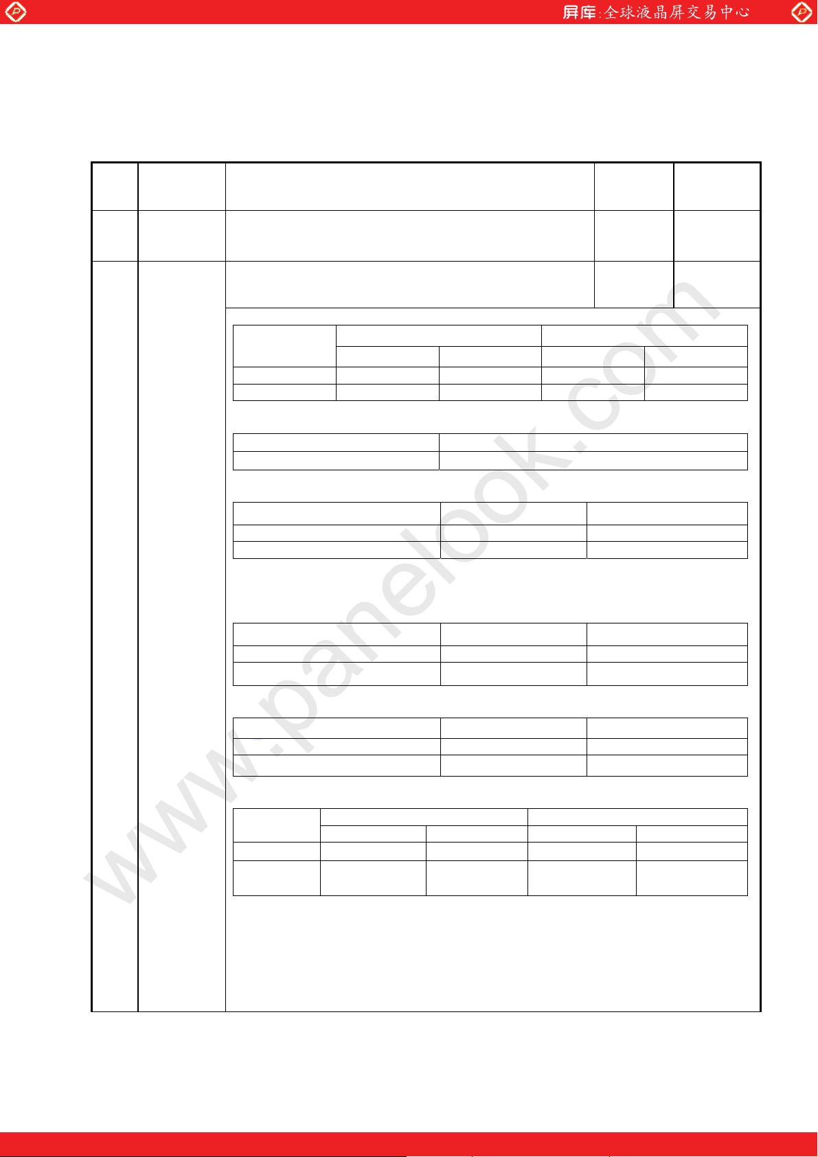
No Date Description Of Changes Rev. no Approval
1 07-04-18 Newly Established. 0.1 Tentative
Total 10 items are revised as below. 1.0 Approval
1. Contrast ratio is changed as below. (5p, 7p)
Condition
NTSC 7,000 : 1 5,500 : 1 7,000 : 1 5,000 : 1
2. Inspection pattern of Cell Defect is changed. (11p)
3. APC Offset level is modified. (13p)
4. GTSEL(Gamma Table Selection) is removed. (17p)
5. Sound Pressure Level is changed. (18p)
2 07-07-31
6. Operational Environmental Condition is changed. (20p)
7. Storage Environmental Condition is changed. (20p)
Condition
Temperature -20ଇ ~ 70ଇ -20ଇ ~ 80ଇ -5ଇ ~ 45ଇ -20ଇ ~ 70ଇ
Pressure
8. Ripple & Noise Spec of Electrical Characteristic is added. (39p)
9. Pin Assignment of connectors for AC Input is added. (41p)
10. Product Label is updated. (48p)
www.panelook.com
Revision History
Before After
Typical Minimum Typical Minimum
PAL 3,500 : 1 2,500 : 1 4,500 : 1 3,500 : 1
Before After
Black Pattern White / R / G / B Pattern
Condition Before After
2/3 Peak Bright Mode 60 h E7 h
1/3 Peak Bright Mode C7 h 1FF h
Condition Before After
Measuring Condition 2,000m 2,300m
Specification 40.xxdB 39.xxdB
Item Before After
Display Operation -5ć ~ 60ć -5ć ~ 55ć
Specification 40.xxdB 39.xxdB
Before After
Recommended Absolute Max Recommended Absolute Max
750 ~ 1013 hPa
307 ~ 1013
hPa
850 ~ 1013 hPa 307 ~ 1013 hPa
SAMSUNG SDI - 2/2 - Rev1.0 31.Jul.07
One step solution for LCD / PDP / OLED panel application: Datasheet, inventory and accessory!
www.panelook.com
Page 3

Global LCD Panel Exchange Center
SAMSUNG SDI Corporation Plasma Display Panel
www.panelook.com
SAMSUNG SDI - 3/3 - Rev1.0 31.Jul.07
One step solution for LCD / PDP / OLED panel application: Datasheet, inventory and accessory!
www.panelook.com
Page 4

Global LCD Panel Exchange Center
SAMSUNG SDI Corporation Plasma Display Panel
TABLE OF CONTENTS
1. DESCRIPTION......................................................................................................................... 6G
2. FEATURES ............................................................................................................................... 6G
3. PRODUCT NAME AND MODEL NUMBER ....................................................................... 6G
4. FUNCTION OUTLINE............................................................................................................ 6G
5. BLOCK DIAGRAM ................................................................................................................. 7G
6. DISPLAY CHARACTERISTICS ........................................................................................... 8G
6.1 DISPLAY PERFORMANCE ........................................................................................................ 8G
6.2 DISPLAY CELL ARRANGEMENT.............................................................................................. 9G
6.3 LUMINANCE MEASUREMENT CONDITION............................................................................. 10G
6.4 CONTRAST MEASUREMENT CONDITION............................................................................... 11G
6.5 DISPLAY CELL DEFECT SPECIFICATION ............................................................................... 12G
6.6 UNIFORMITY SPECIFICATIONS.............................................................................................. 13G
6.7 POWER CONSUMPTION ......................................................................................................... 13G
6.8 GAMMA CHARACTERISTICS.................................................................................................. 17G
www.panelook.com
7. SOUND PRESSURE LEVEL SPECIFICATION .............................................................. 19G
7.1 MEASUREMENT CONDITION................................................................................................. 19G
7.2 SOUND PRESSURE LEVEL ..................................................................................................... 19G
8. MECHANICAL CHARACTERISTICS............................................................................... 20G
8.1 MECHANICAL SPECIFICATIONS ............................................................................................ 20G
8.2 MECHANICAL CHARACTERISTICS......................................................................................... 20G
9. ENVIRONMENTAL CONDITIONS ................................................................................... 21G
9.1 OPERATIONAL ENVIRONMENTAL CONDITION ...................................................................... 21G
9.2 STORAGE ENVIRONMENTAL CONDITION (*1)..................................................................... 21G
9.3 PANEL SURFACE CONDITION............................................................................................... 22G
10. INTERFACE SIGNAL SPECIFICATIONS...................................................................... 23G
10.1 INTERFACE CONFIGURATION ............................................................................................. 23G
10.2 INTERFACE FUNCTION SPECIFICATIONS (INPUT DATA AND DISPLAY PROCESSING)............. 24G
10.3 INPUT SIGNAL DEFINITION................................................................................................. 24G
10.4 LVDS SIGNAL DEFINITION AND FUNCTION....................................................................... 24G
10.5 LVDS SIGNAL PIN ASSIGNMENT ....................................................................................... 27G
10.6 VIDEO SIGNAL DEFINITION AND FUNCTION ....................................................................... 28G
10.7 ELECTRICAL CONDITION OF INTERFACE SIGNAL................................................................ 29G
10.8 VIDEO SIGNAL INTERFACE TIMING FORMATS.................................................................... 30G
10.9 LVDS CONNECTION SPECIFICATIONS................................................................................ 32G
10.10 I2C INTERFACE CONDITIONS ........................................................................................... 33G
10.11 CONNECTOR SPECIFICATIONS .......................................................................................... 37
SAMSUNG SDI - 4/4 - Rev1.0 31.Jul.07
One step solution for LCD / PDP / OLED panel application: Datasheet, inventory and accessory!
www.panelook.com
Page 5

Global LCD Panel Exchange Center
SAMSUNG SDI Corporation Plasma Display Panel
www.panelook.com
11.REGISTER MAP................................................................................................................... 38
11.1 ADDRESS MAP ................................................................................................................... 38G
11.2 DETAILED SETTINGS .......................................................................................................... 39G
12. INPUT POWER VOLTAGE SPECIFICATIONS ............................................................ 40G
12.1 ELECTRICAL CHARACTERISTIC OVERVIEW ........................................................................ 40G
12.2 ELECTRICAL CHARACTERISTIC OVERVIEW FOR IMAGE BOARD ......................................... 40G
12.3 PIN ASSIGNMENT OF CONNECTORS FOR POWER SUPPLY..................................................... 41G
12.4 PIN ASSIGNMENT OF CONNECTORS FOR IMAGE BOARD ...................................................... 42G
13. MECHANICAL DIMENSION DRAWING....................................................................... 48G
13.1 FRONT SIDE ....................................................................................................................... 48G
13.2 REAR SIDE ......................................................................................................................... 48G
14. LABEL ................................................................................................................................... 49G
14.1 LABEL TYPE....................................................................................................................... 49G
14.2 LABEL LOCATION............................................................................................................... 50G
15. PACKING.............................................................................................................................. 51G
16. RELIABLITY ....................................................................................................................... 52G
16.1 MTBF VALUE ................................................................................................................... 52G
16.2 EXPECTED SERVICE LIFETIME............................................................................................ 52G
16.3 DISCLAIMER...................................................................................................................... 53G
16.4 CERTIFICATE...................................................................................................................... 53G
G
17. WARNING / CAUTION / NOTICE ................................................................................... 54G
17.1 WARNING .......................................................................................................................... 54G
17.2 CAUTION............................................................................................................................ 56G
17.3 NOTICE .............................................................................................................................. 57G
SAMSUNG SDI - 5/5 - Rev1.0 31.Jul.07
One step solution for LCD / PDP / OLED panel application: Datasheet, inventory and accessory!
www.panelook.com
Page 6

Global LCD Panel Exchange Center
SAMSUNG SDI Corporation Plasma Display Panel
1. DESCRIPTION
The S63FH-XD01 is a 63-inch wide full color plasma display Module with a resolution of
1920(H) × 1080(V) pixels. The display module includes the Plasma Display Panel,
the Panel Driving Electronics, the Logic Control Board.
2. FEATURES
x Wide aspect ratio(16:9) in 63 inch diagonal display screen. The display area is
1393.92mm wide and 784.08mm high.
x Slim and light weight. The display module is 70.1mm in depth and weighsonly
approx. 41.4kg.
x 68719.47 million colors(12Bit), 1073.7 million colors(10Bit), or 16.77 million
colors(8Bit) combination of R,G and B digital data.(according to LVDS input selection)
x High Luminance, High contrast, Wide viewing angle. The screen has a white peak
luminance of typical 1,000 cd/້( NTSC,PAL), contrast of typical 7,000:1(NTSC),
4,500:1(PAL). The viewing angle of 160° or greater is achieved.
www.panelook.com
3. PRODUCT NAME AND MODEL NUMBER
x Product name : 63 inch Full Color Plasma Display Module1
(abbreviation : PDP Module1)
x Model number : S63FH-XD01
x Product Code :
PP63FH001A
4. FUNCTION OUTLINE
x The plasma display module has an APC(Automatic Power Control) function which
restricts power consumption within a certain range with respect to each display load ratio.
x The plasma display module is operated by input digital video signals; vertical
synchronous signal (vsync), horizontal synchronous signal (hsync), data enable signal
and 8~12bits data signal for the respective R,G, and B color. All digital video signals are
transferred by a LVDS cable.
x The plasma display module is operated at 60Hz/50Hz frame rate.
x The plasma display module requires several levels of input power voltages respectively
for the logic main, the TCP’s, the gate drivers, the sustain switches, the column drivers,
Y-Set, Y-scan, and X-bias.
x The plasma display module is operated at progressive scan video input signal only.
An external progressive scan conversion is required in order to display the other formats.
SAMSUNG SDI - 6/6 - Rev1.0 31.Jul.07
One step solution for LCD / PDP / OLED panel application: Datasheet, inventory and accessory!
www.panelook.com
Page 7
Global LCD Panel Exchange Center
SAMSUNG SDI Corporation Plasma Display Panel
5. BLOCK DIAGRAM
LOGIC CONTROLLER
www.panelook.com
LVDS SIGNAL
LVDS I/F CONTROLLER
DATA PROCESSOR
DISPLAY DATA
DRIVING CIRCUIT AND PANEL
SCAN PULSE
DRIVER
PDP
1920Ý1080 Pixels
SUSTAIN PULSE
DRIVER
Figure-1. Block Diagram of PDP module
DATA DRIVER
DRIVING VOLTAGE
SAMSUNG SDI - 7/7 - Rev1.0 31.Jul.07
One step solution for LCD / PDP / OLED panel application: Datasheet, inventory and accessory!
www.panelook.com
Page 8
Global LCD Panel Exchange Center
SAMSUNG SDI Corporation Plasma Display Panel
6. DISPLAY CHARACTERISTICS
6.1 Display Performance
No Item Rating
www.panelook.com
1
2
3
4
5
6
7
8
Display Pixels
Display Cells Horizontal 5,760 cells ×Vertical 1,080 cells
Pixel Pitch Horizontal 0.726mm × Vertical 0.726mm
Cell Size
Pixel Type R, G, B Non stripe (refer to Figure-2)
Effective Display
Size
Number of color
Peak Luminance *1
(peak algorithm on)
Contrast Ratio *2
9
10
(in dark room,
peak algorithm on)
Brightness
(Full white Brightness)
Horizontal 1,920 ×Vertical 1,080 pixels
(1 pixel = 1 R,G,B cells)
R Horizontal 0.242mm × Vertical 0.726mm
G Horizontal 0.242mm × Vertical 0.726mm
B Horizontal 0.242mm × Vertical 0.726mm
Horizontal 1393.92mm ×Vertical 784.08mm
[ 54.88 inch (H) × 30.87 inch (V) ]
68719.47 million colors (12Bit)
1073.7 million colors (10Bit)
16.77 million colors ( 8Bit)
NTSC:Typical 1,000 cd/້ , Minimum 900 cd/້
PAL: Typical 1,000 cd/້ , Minimum 900 cd/້
NTSC:Typical 7,000:1, Minimum 5,000:1
PAL: Typical 4,500:1, Minimum 3,500:1
NTSC:Typical 170cd/້ , Minimum 155 cd/້
PAL: Typical 170cd/້ , Minimum 155 cd/້
11
Viewing Angle *3 Over 160°
(Note)
* 1. The luminance and color coordinates are measured at a full white pattern (load ratio
100%). The condition for measurement is shown in Figure-3.
* 2. The contrast ratio is calculated from the display luminance and the non-display
luminance value. Display condition is shown in Figure-4.
* 3. The viewing angle is a critical angle at which the observed luminance is reduced to
30% to the luminance perpendicular to the PDP module. The luminance is measured
by a non-contact luminance meter BM-7.
SAMSUNG SDI - 8/8 - Rev1.0 31.Jul.07
One step solution for LCD / PDP / OLED panel application: Datasheet, inventory and accessory!
www.panelook.com
Page 9
Global LCD Panel Exchange Center
SAMSUNG SDI Corporation Plasma Display Panel
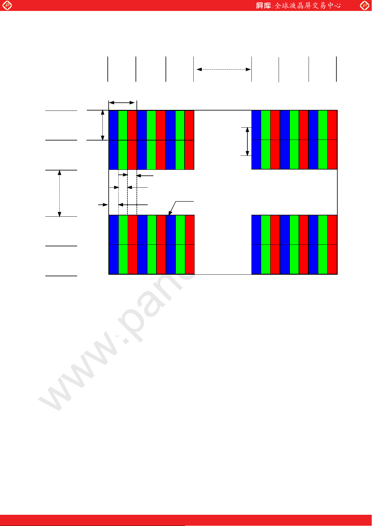
6.2 Display Cell Arrangement
www.panelook.com
1st
Pixel
Row
2nd
Pixel
Row
1079th
Pixel
Row
1st
Pixel
Column
Pixel Pitch (Width): 0.726 mm
Pixel
Pitch
2nd
Pixel
Column
ڭڢڝ ڭڢڝ ڭڢڝ
ڭڢڝ ڭڢڝ ڭڢڝ
31575
31575
31575
ڭڢڝ ڭڢڝ ڝڢڭ
3rd
Pixel
Column
ڞۀۇۇ
ګۄۏھۃ ڣۀۄ ۂۃ ۏ
ڃڋډڒڍڑ ۈۈڄ
1918th
Pixel
Column
1919th
Pixel
Column
ڭڢڝ ڭڢڝ ڝڢڭ
ڭڢڝ ڭڢڝ ڭڢڝ
ڭڢڝ ڭڢڝ ڭڢڝ
1920th
Pixel
Column
1080th
Pixel
Row
ڭڢڝ ڭڢڝ ڭڢڝ
Figure-2.Display Cell Arrangement
ڭڢڝ ڭڢڝ ڭڢڝ
SAMSUNG SDI - 9/9 - Rev1.0 31.Jul.07
One step solution for LCD / PDP / OLED panel application: Datasheet, inventory and accessory!
www.panelook.com
Page 10
Global LCD Panel Exchange Center
SAMSUNG SDI Corporation Plasma Display Panel
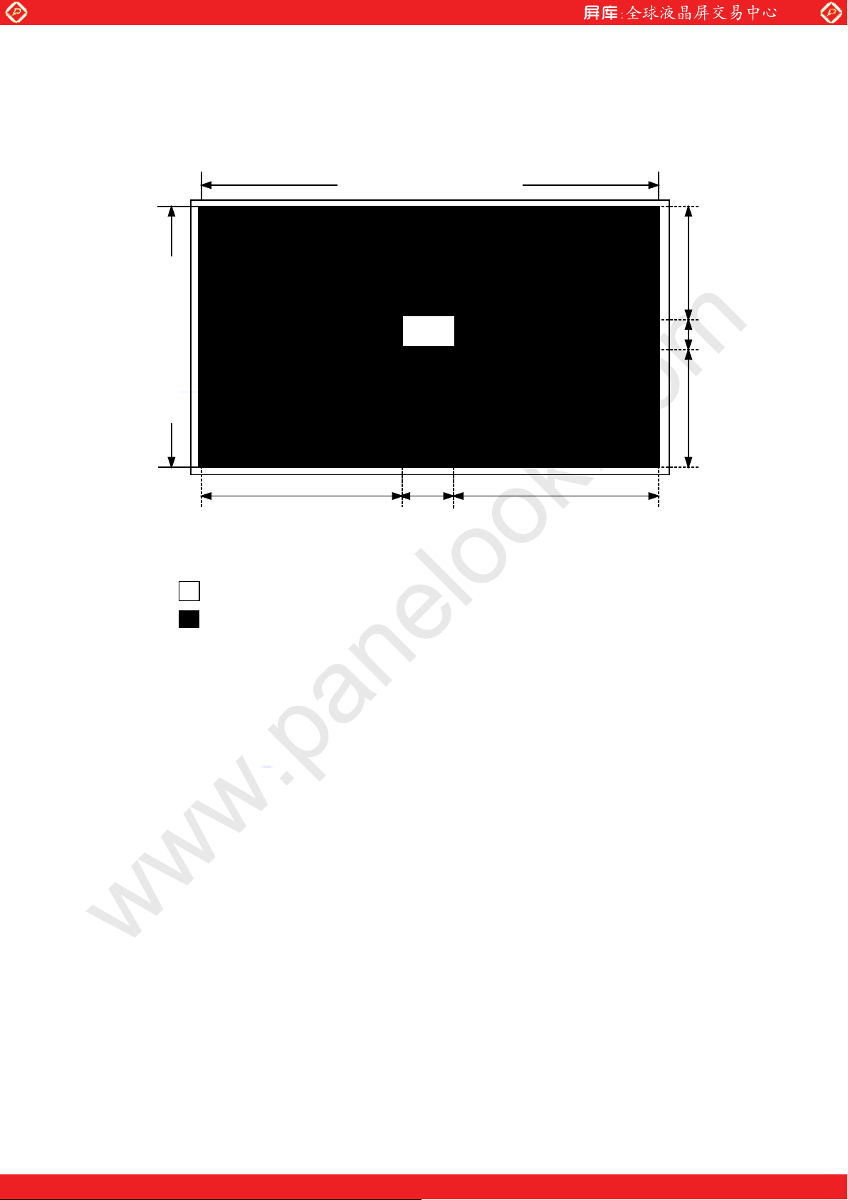
6.3 Luminance Measurement Condition
(1) Display Pattern
www.panelook.com
Effective Display Area
Effective Display Area
864 192 864
Unit : Pixels(=lines)
marked area : White display area by maximum gradation setting
marked area : Black color (non-display area)
Figure-3. Display Pattern for Brightness & Contrast Ratio Measurement
(2) Display area ratio : 1% white window
(3) Vsync : 16.7ms
(4) Measuring equipment : MINOLTA CA-100Plus
Pattern Generator(VG-828, LVDS Output).
(5) Ambient Temperature : Room Temperature
(6) Ambient Luminance : Dark Room (<2 lux)
[ Note]
1. Measured within 30 seconds after a power-on. The temperature of the panel before the
measurement is a room temperature (25 ).ć
2. Measured done within 3 seconds after the pattern starts being displayed. (
486
108
486
Figure-3)
SAMSUNG SDI - 10/10 - Rev1.0 31.Jul.07
One step solution for LCD / PDP / OLED panel application: Datasheet, inventory and accessory!
www.panelook.com
Page 11
Global LCD Panel Exchange Center
SAMSUNG SDI Corporation Plasma Display Panel
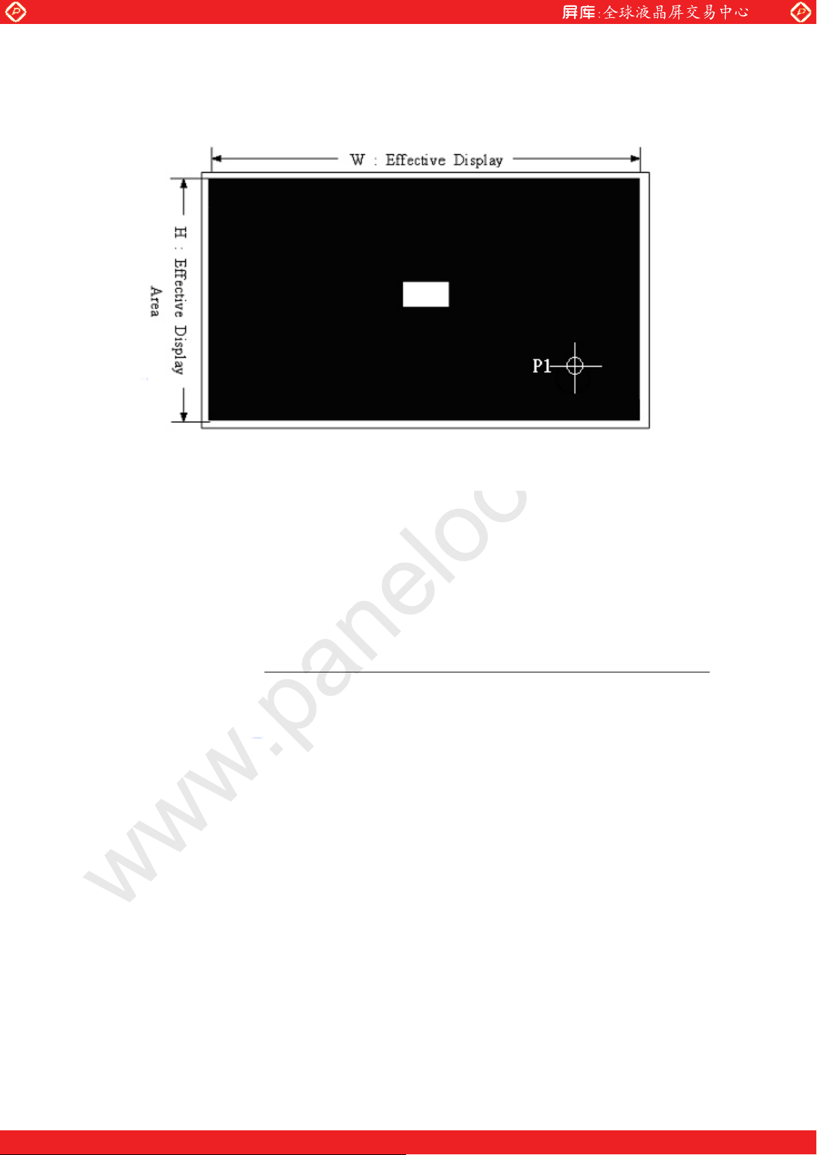
6.4 Contrast Measurement Condition
(1) Measuring point
www.panelook.com
Figure-4. Measurement point
(2) Vsync : 16.7 ms
(3) Measuring Equipment : MINOLTA CA-100Plus
Pattern Generator(VG-828, LVDS Output).
(4) Contrast Calculation formula
Luminance of 1% white window area at the center of the screen
Contrast ratio =
Luminance of black area
ૺ Note ૻ
1. For mass production test purposes, it is recommended to measure only the
single point, P1 of Fig. 4 at the display pattern of Fig.3.
2. The measurement point P1 is the minimum luminance point inside the effective
display area.
(5) Ambient light condition : dark room ( <2 lux )
SAMSUNG SDI - 11/11 - Rev1.0 31.Jul.07
One step solution for LCD / PDP / OLED panel application: Datasheet, inventory and accessory!
www.panelook.com
Page 12
Global LCD Panel Exchange Center
SAMSUNG SDI Corporation Plasma Display Panel
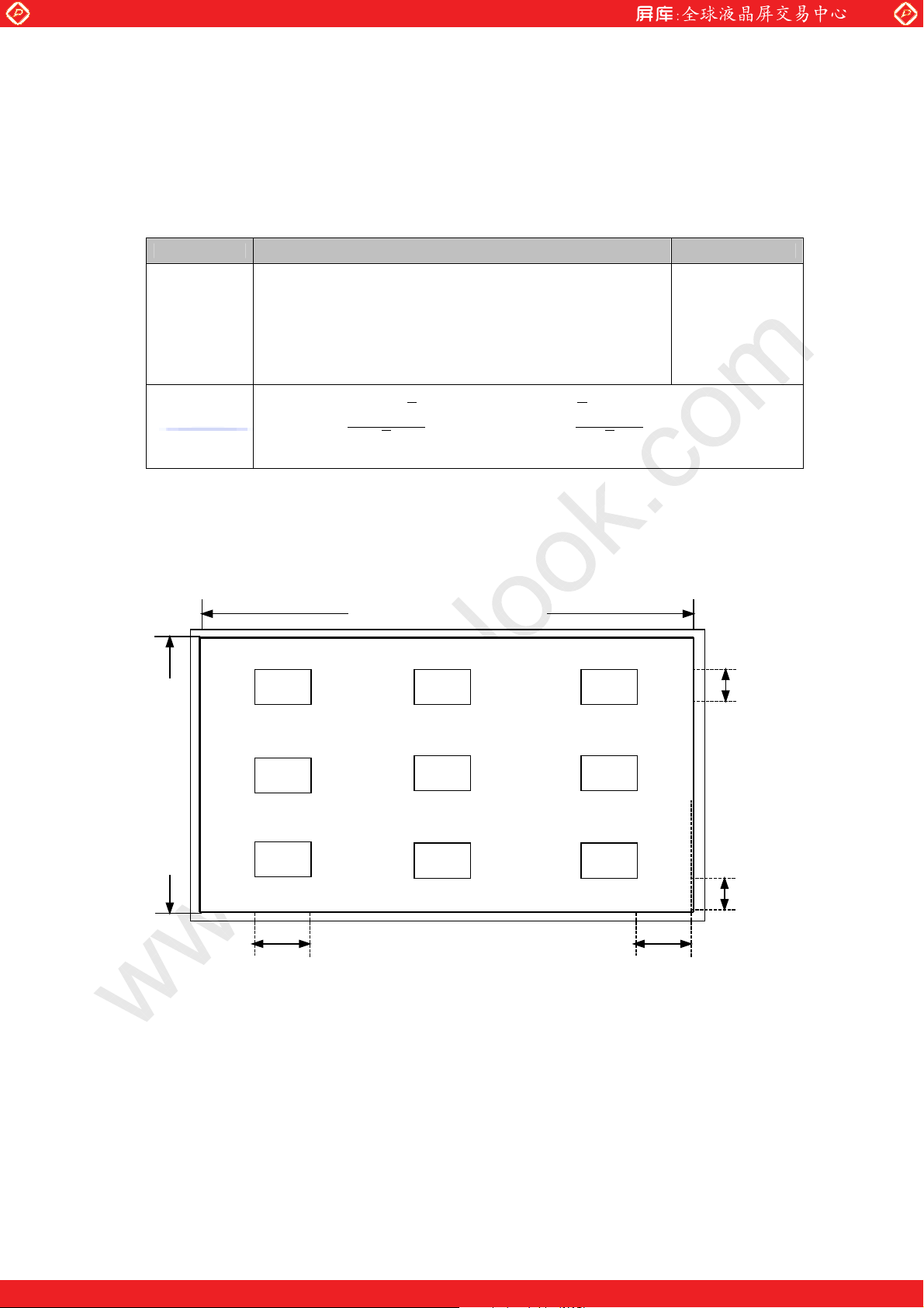
6.5 Display Cell Defect Specification
In some cases, a panel may have defective cells produced in panel-making processes.
These defective cells can be categorized into three types;
(1) Non-lighting cell defect : defect in which the cell is always off
(2) Non-extinguishing cell defect : defect in which the cell is always on.
(3) Flickering cell defect : defect in which the cell flickers.
(4) High intensity cell defect : defect in which the cell is brighter than neighboring cells
(5) Test pattern : Full White, Full Red, Full Green and Full Blue with 1023 gray level.
The display cell defect specifications define the allowed limits for the number of the cell
defects and are used as the criteria to determine whether the panel in concern should be
delivered to a customer.
www.panelook.com
Figure-5. Measurement Area
Number of cell defects
Item
Non-lighting cell
Non-extinguishing cell
Flickering cell
(White/Red/Green/Blue pattern)
Flickering cell
(the other pattern)
High Intensity Cell
Total defect
A Zone B Zone
3 and less 10 and less
1 2 and less
2 3 and less
1 2 and less
1 2 and less
13 and less
Regardless of A and B
Zone,
Maximum 1 Cell Defect
in an area of 50*50mm
is allowed.
Remark
SAMSUNG SDI - 12/12 - Rev1.0 31.Jul.07
One step solution for LCD / PDP / OLED panel application: Datasheet, inventory and accessory!
www.panelook.com
Page 13
Global LCD Panel Exchange Center
x
SAMSUNG SDI Corporation Plasma Display Panel
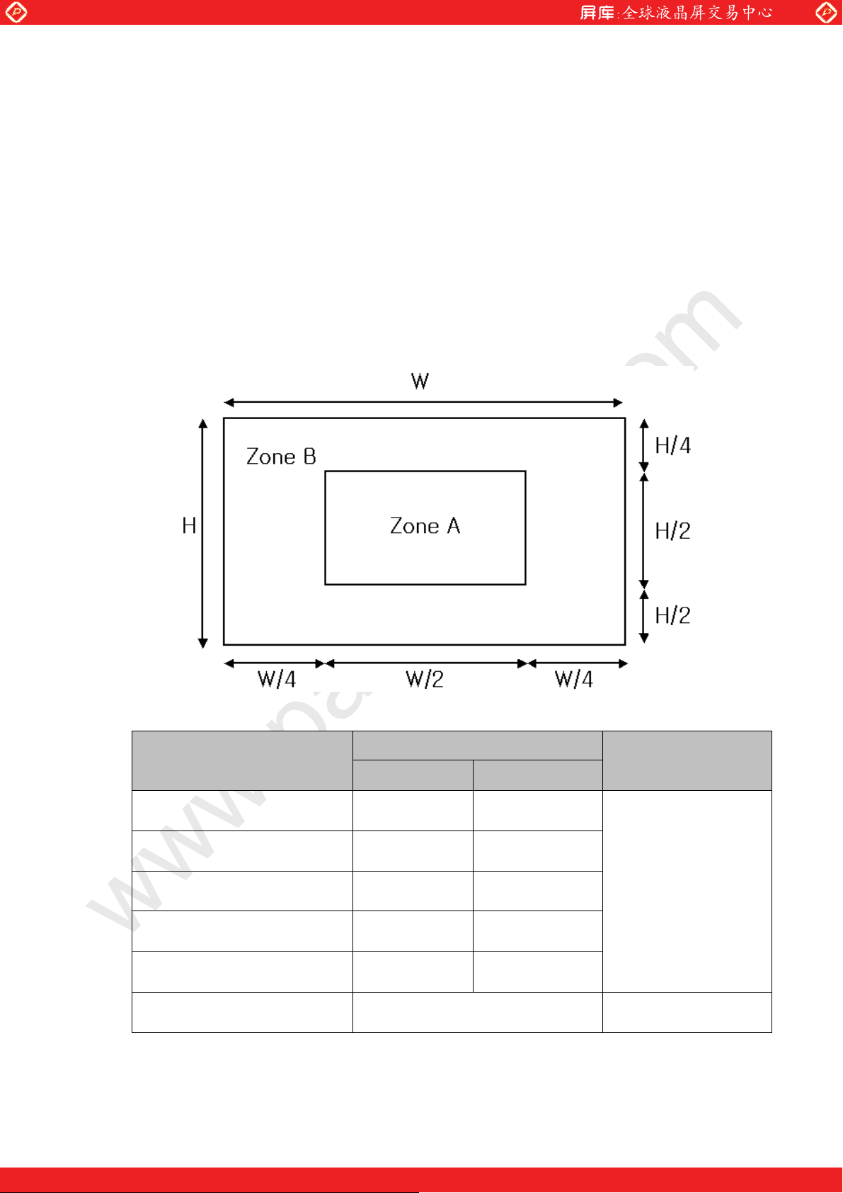
6.6 Uniformity Specifications
The color-PDP uses a ultraviolet light produced by a series of gas discharges to illuminate
the phosphor material inside the panel.
Non-uniform phosphor coating and variations of discharge characteristics may result in a
slight difference of brightness depending on the positions inside a panel.
www.panelook.com
Item
Full white
brightness
variation
Equation
Definition
The brightness is measured at 9 points (A1~A9 of
Fig. 6) on full white pattern. The full white brightness
variation iss then calculated from the following
equations where x-bar is the measured value .
Max xx
xMin
u 100%
&
Specification
10% and less
u 100%
The brightness variation specifications define the allowed limits for brightness differences
used as the criteria in determining whether the panel is delivered to a customer.
W : Effective Display Area
H : Effective Display Area
A1 A2 A3
H*0.1
A4
A7
W*0.1
Figure-6. Measuringareas
A5 A6
A8 A9
H*0.1
W*0.1
6.7 Power consumption
SAMSUNG SDI - 13/13 - Rev1.0 31.Jul.07
One step solution for LCD / PDP / OLED panel application: Datasheet, inventory and accessory!
www.panelook.com
Page 14
Global LCD Panel Exchange Center
d
SAMSUNG SDI Corporation Plasma Display Panel
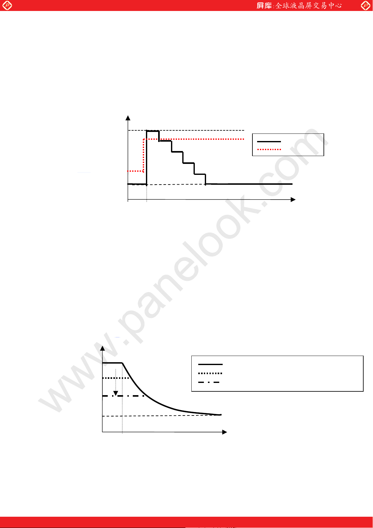
1) APC (Automatic Power Control) Function
The module has an APC (Automatic Power Control) function for the panel driver power
source. When the total display load ratio exceeds approximately 10%, total power
consumption is limited within a specified level(=Lower Power Limit) by APC function.
The operation behaviour of APC function is called as SLOW-APC. When the display
load-ratio changes from a low to a high value, the power-consumption rises instantly to
“Upper Power Limit” and gradually decreases until it reachs to the “Lower Power Limit”.
[Note] Number of steps may vary as a function of the load ratio.
Power
Upper Power
Limit
Lower Power
Limit
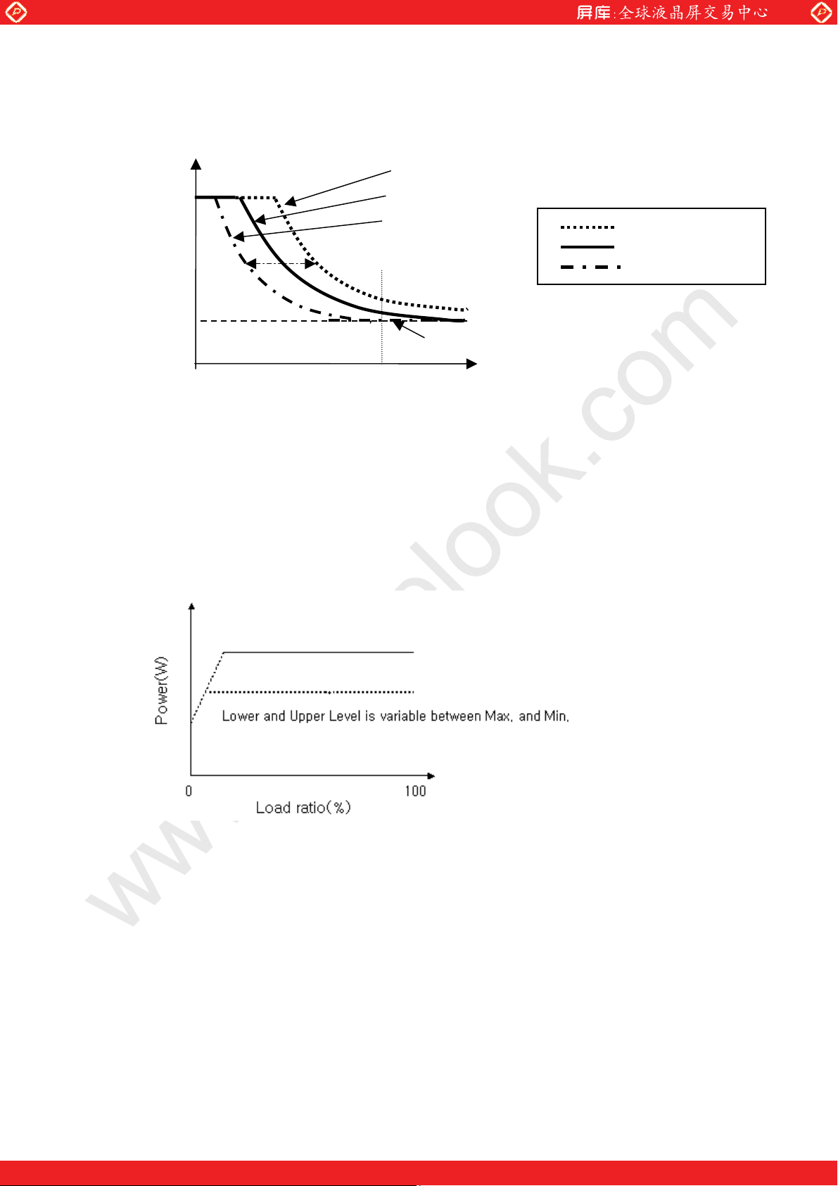
2) Brightness and Power Mode Control
This module offsers two methods for brightness and power mode control.
One is APCO(APC Offset) for Peak-Brightness control, and the others are PUG and
PLG
for power mode control. APCO(89C0h) and PLG(89DAh) are registers controllable
through I2C communication from an image B’d. For the detailed explanations of these
registers, refer to the Chapter 11. Register Map.
(1) Peak-Brightness Control( APCO)
- controls the max.sustain number
- APCO variable range : 00~C7h
Sustain
num
ber
Max. Sustain
Min. Sustain
0 100%
Cmax
(2) ASLG(89C6h) ( Power-Mode Control using ASL gain function)
www.panelook.com
Figure-8 Slow APC Behaviour
load ratio
Power
Loa
-ratio
Time for transition between 2 setps = 8 frames
(This could be controlled by R_HOLD_TIME)
t
Normal Bright Mode (APCO=00h)
66% Peak-bright Mode (APCO=E7h)
25% Peak-bright Mode (APCO=1FFh)
Figure 8. APCO Behavior
SAMSUNG SDI - 14/14 - Rev1.0 31.Jul.07
One step solution for LCD / PDP / OLED panel application: Datasheet, inventory and accessory!
www.panelook.com
Page 15
Global LCD Panel Exchange Center
)
g
r
N
d
SAMSUNG SDI Corporation Plasma Display Panel
- ASLG variable range : 80h~FFh
- Maximum available power decrease by increasing ASLG above 80h(NTSC)
Sustain
number
Max. Sustain
Min. Sustain
0
Loa
-
www.panelook.com
ASLG < ASLG’
ASLG’ = 60h@NTSC(50h@PAL
ASLG > ASLG’
load at F/W pattern
Saturated at Min. Sustain
-ratio 100%
Hi
h-Power Mode
or al Modem
Powe
-Save Mode
(3) Power-Mode Control via PLG
- PLG(Power Lower Gain control register)
- Variable range : 00 ~ 80h(Tentative) , Default Value : 80
Typical : 650W
Min : 600W
Figure 10. APC Behavior(PLG Adjusted)
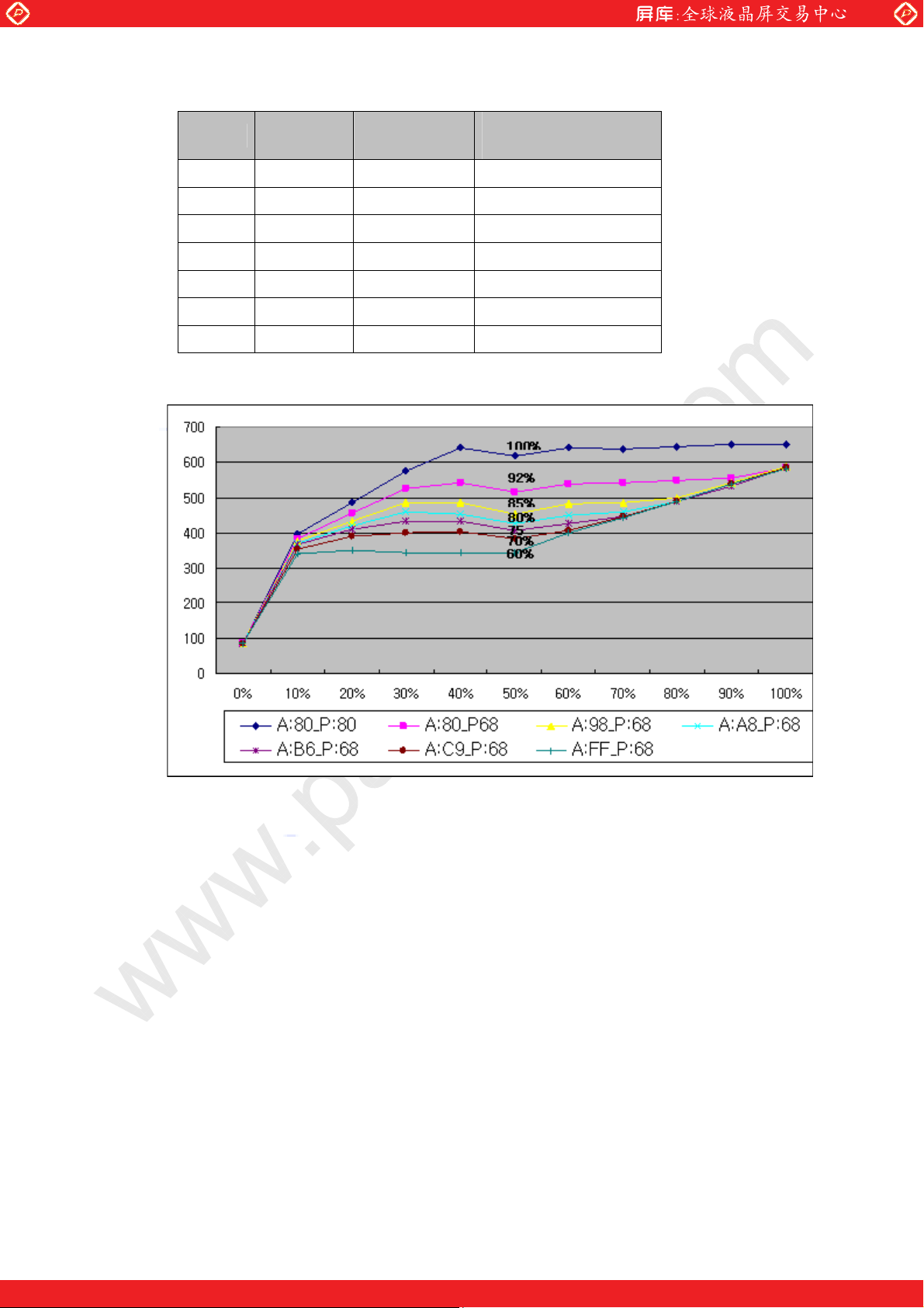
(4) Power- Consumption Ratio( BY ASLG, PLG)
SAMSUNG SDI - 15/15 - Rev1.0 31.Jul.07
One step solution for LCD / PDP / OLED panel application: Datasheet, inventory and accessory!
www.panelook.com
Page 16
Global LCD Panel Exchange Center
SAMSUNG SDI Corporation Plasma Display Panel
PLG ASLG ASLG_SW
80 80 OFF 100%
74 80 OFF 90%
6C 8B OFF 86%
6C 93 ON 80%
6C A9 ON 70%
6C DC ON 60%
6C FF ON 55%
ૺ Note ૻ Condition By Moving Picture(30% Window Size)
www.panelook.com
Power- Consumption
Ratio
Figure 11. Power- Consumption Ratio by the window size(Load Ratio)
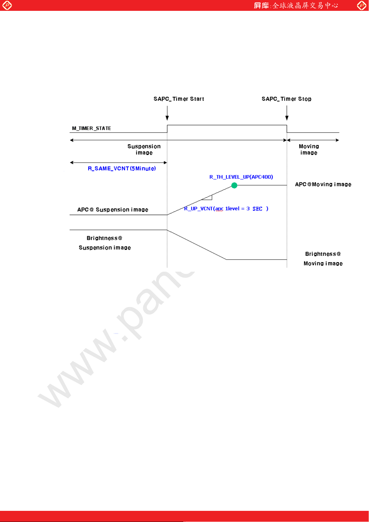
(5) APC_Timer
The module is equipped with the APC Timer function to reduce the amount of image
SAMSUNG SDI - 16/16 - Rev1.0 31.Jul.07
One step solution for LCD / PDP / OLED panel application: Datasheet, inventory and accessory!
www.panelook.com
Page 17
Global LCD Panel Exchange Center
SAMSUNG SDI Corporation Plasma Display Panel
retention. If the input image is not varying for at least five minutes, the fuction starts to
operate and reduce the intial APC level one step down to a predefined target level in
every three seconds. The fuction is immediately turned off when the input image starts
varying.
www.panelook.com
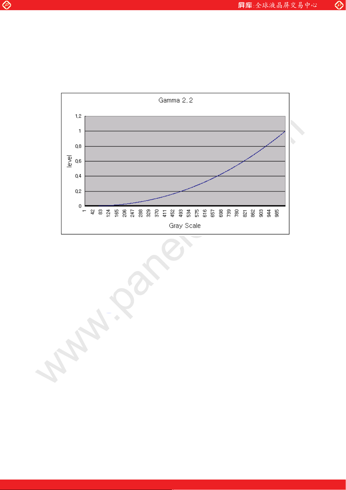
6.8 Gamma characteristics
The module offers a variety of preset gamma’s, as well as a direct control by a customer.
The registers regarding gamma selection and control are adjustable through I2C
SAMSUNG SDI - 17/17 - Rev1.0 31.Jul.07
One step solution for LCD / PDP / OLED panel application: Datasheet, inventory and accessory!
www.panelook.com
Page 18
Global LCD Panel Exchange Center
SAMSUNG SDI Corporation Plasma Display Panel
communication from an image B’d. For detailed addresses and explanation of the registers,
refer to the Chapter 11. Register Map.
1) Basic gamma curve
The module is initially set to a default 2.2 gamma curve (refer to Figure. 12)
However, the initial gamma setting could be adjusted to any values at the request of a
the customer.
www.panelook.com
Figure-12. Default Gamma Curve
SAMSUNG SDI - 18/18 - Rev1.0 31.Jul.07
One step solution for LCD / PDP / OLED panel application: Datasheet, inventory and accessory!
www.panelook.com
Page 19
Global LCD Panel Exchange Center
SAMSUNG SDI Corporation Plasma Display Panel
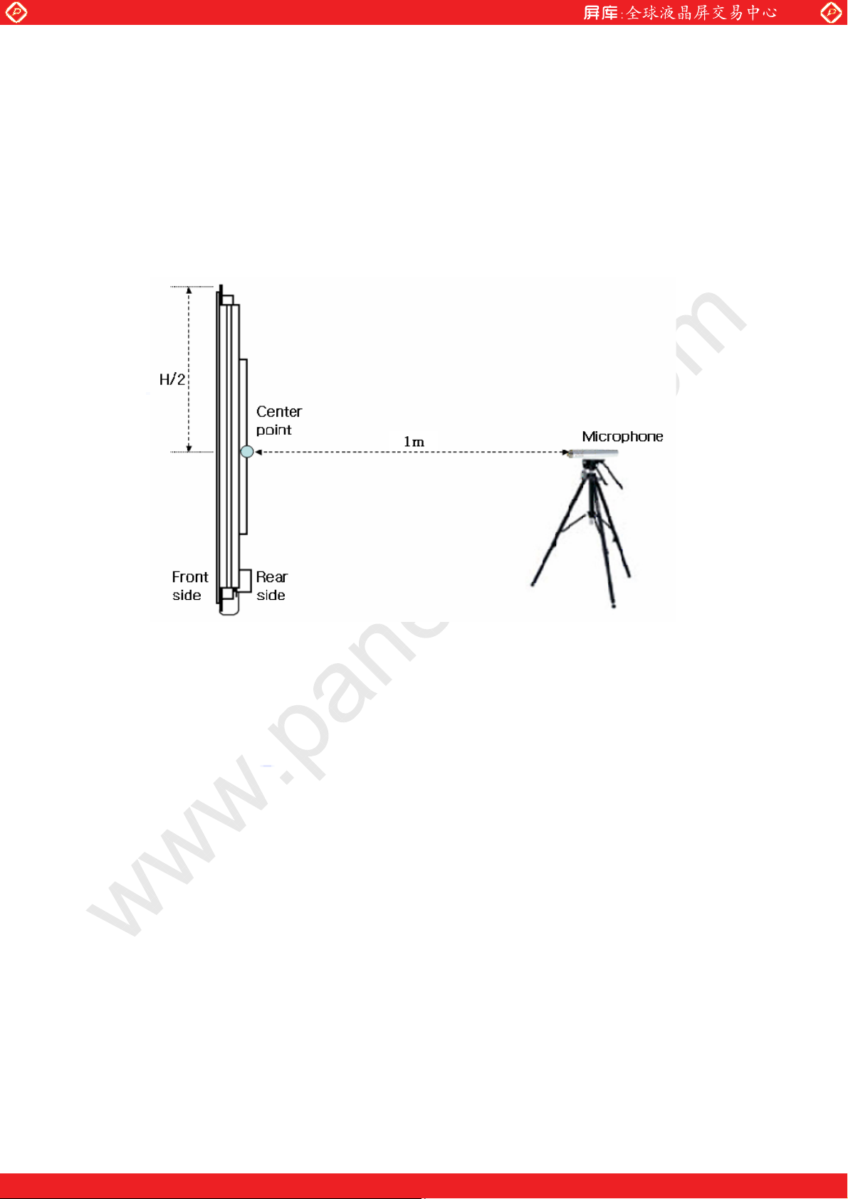
7. SOUND PRESSURE LEVEL SPECIFICATION
7.1 Measurement Condition
(1) Background Noise Level : less than 20dB (Anechoic chanber)
(2) Measuring Pattern : Full White
(3) Measuring Equipment : Sound level meter Type 2827 made by B&K
(4) Measuring Distance : 1.0m from the rear side of the module
(5) Measuring point
www.panelook.com
Figure-13. Measuring Point
7.2 Sound Pressure Level
(1) Level Ground (Land)
-. Measuring Condition : 0 meter
-. Sound Pressure Level is overall level caculated from the individual band levels of
50Hz ~ 8kHz.
-. Specification : 30.xx dB (max.)
(2) High Ground
-. Measuring Condition :
-. Sound Pressure Level is overall level caculated from the individual band levels of
4 ~ 12.5 KHz.
-. Specification : 39.xx dB (max.)
[ Note ]
1. SDI recommends that the back cabinet of a TV has the ventilation holes of less than
2.7 mm in diameter.
2. Audible noise is guaranteed till the altitude of 2,300 meter.
3. In order to guarantee audible noise at higher altitude than 2,300 meter, a special
module has to be used.
2,300 meter
SAMSUNG SDI - 19/19 - Rev1.0 31.Jul.07
One step solution for LCD / PDP / OLED panel application: Datasheet, inventory and accessory!
www.panelook.com
Page 20

Global LCD Panel Exchange Center
SAMSUNG SDI Corporation Plasma Display Panel
8. MECHANICAL CHARACTERISTICS
8.1 Mechanical Specifications
No Item Rating
Outer
1
Dimension
2 Weight Approximatly 41.4 kg
8.2 Mechanical Characteristics
No Item Rating
www.panelook.com
Width 1484 ໄ × Height 875 ໄ × Thickness 70.1 ໄ
(including FPC and TCP)
*see appendix : Mechanical Dimension Drawing
Frequency : 10 ~ 55 Hz
1 Vibration
2 Shock
Sweep Rate : 1 Octave/min
Stroke : x,y direction : 0.35 mm
Z direction : 0.175 mm
Acceleration : less than 20 G (x,y direction)
less than 10 G (z direction)
Duration Time : 11 ms
* Notes: ( Test condition ) Non-Packaging, Operational (only for Vibration)
* Test time of Vibration Test is 30 minutes for every direction(x,y,z)
* The number of times for the shock test is 6 times for every direction(x,y,z).
SAMSUNG SDI - 20/20 - Rev1.0 31.Jul.07
One step solution for LCD / PDP / OLED panel application: Datasheet, inventory and accessory!
www.panelook.com
Page 21

Global LCD Panel Exchange Center
SAMSUNG SDI Corporation Plasma Display Panel
9. ENVIRONMENTAL CONDITIONS
9.1 Operational Environmental Condition
No Item Rating
temperature
2 Panel Surface
Temperature *3
3 Humidity Display Operation 20 ~ 80 RH (no condensation)
4 Pressure Display Operation 0 ~ 2,300 m
[NOTE]
1. Functional operation refers to only the electrical function of the module.
2. Display operation refers to both the display and the electrical functions of the module.
3. Panel surface temperature is measured at a normal display mode in a room
temperature (25 ). Due to the discharge heat dissipation inside the panel, the temperature ć
appears to become higher for small size pattern ( large sustain pulses )
The judgement of display defects (e.g. weak discharge, discharge error) must be performed
at an ambient temperature defined in this table.
4. Audible noise is guaranteed up to 2,300m.
www.panelook.com
Display Operation -5ć ~ 55ć 1 Ambient
Temperature Slope Below 1.5 ć/minute
Small Size Pattern
Full White Pattern
Temperature Slope Below 20 ć/cm
~ 120 ć
~ 85 ć
9.2 Storage Environmental Condition (*1)
No Item
1 Temperature
2 Humidity
3 Pressure
[NOTE]
*1. By the term Storage, we refer to a period of relatively short time for shipping and handling.
(e.g. transportation, relocation and etc.)
SAMSUNG SDI - 21/21 - Rev1.0 31.Jul.07
Recommended Absolute maximum
-5ć ~ 45ć -20ć ~ 70ć
20 ~ 80% RH 5 ~ 85% RH
850 ~ 1013 hPa 307 ~ 1013 hPa
Rating
One step solution for LCD / PDP / OLED panel application: Datasheet, inventory and accessory!
www.panelook.com
Page 22

Global LCD Panel Exchange Center
SAMSUNG SDI Corporation Plasma Display Panel
9.3 Panel Surface Condition
1) Specification for the surface temperature of panel
The panel surface temperature should be kept as below in order to guarantee a stable
display function of input images.
- Tp= below 120 (Absolute Maximum Rating); whenć small size of image is displayed
- Tp= below 85 ; when Full White is displayed.ć
If the temperature exceeds above level, it may cause the defects of displayed images such
as dot defect, line defect, and/or poor image quality.
As the surface temperature of panel tends to rise with deduction of display rate,
the relation with temperature can be described as below:
85 (display load rate is high : large area )ć
Figure-14. Surface Temperature Vs Displayed Area
Surface
Temperature
120
85ଇ
It is strongly recommended that the panel surface temperature should be kept as low as
possible, even though its maximium rating is described as above.
2) Panel Surface Temperature for Breaking
The temperature uniformity across a panel should be maintained below minum of
20 /ć in order not to prevent panel from being broken. However, the threshold 20 /ć
of the temperature gradient inducing cracks could not be precisely specified since the
panel cracking also depends critically on own initial conditions such as scratches.
Please take the threshold value as a reference.
www.panelook.com
~ 120 (display load rate is low : small area)ć
15~20% 100%
Displayed
SAMSUNG SDI - 22/22 - Rev1.0 31.Jul.07
One step solution for LCD / PDP / OLED panel application: Datasheet, inventory and accessory!
www.panelook.com
Page 23

Global LCD Panel Exchange Center
K
K
Pdvwhu#
Vodyh#
SAMSUNG SDI Corporation Plasma Display Panel
10. INTERFACE SIGNAL SPECIFICATIONS
10.1 Interface Configuration
Image scale b’d
www.panelook.com
Tx/RxO0±
Tx/RxO1±
Tx/RxO2±
Tx/RxO3±
Tx/RxO4±
Tx/RxO5±
Tx/RxOCL
Tx/RxE0±
Tx/RxE1±
Tx/RxE2±
Tx/RxE3±
Tx/RxE4±
Tx/RxE5±
Tx/RxECL
±
±
PDP Module
zwzTopW]G
G
G
Right R0-R11
Right G0-G11
Right B0-B11
Vsync
Hsync
ENABLE
DLCK
R0-R11
G0-G11
B0-B11
Vsync
Hsync
ENABLE
DLCK
Tx
s}kzG {G
G
G
Rx
SDA
SCL
I2C READY
IMG EINT
tG
G
G
Left R0-R11
zwzTopW]G
G
G
Left G0-G11
Left B0-B11
Vsync
Hsync
ENABLE
DLCK
Figure-15. Interface Block Diagram
SAMSUNG SDI - 23/23 - Rev1.0 31.Jul.07
One step solution for LCD / PDP / OLED panel application: Datasheet, inventory and accessory!
www.panelook.com
Page 24

Global LCD Panel Exchange Center
SAMSUNG SDI Corporation Plasma Display Panel
10.2 Interface Function Specifications (input data and display processing)
- 1920x1080-dot data and timing signals (video signal) should be provided to the
module in order to display images.
- The video signal receiving block is implemented by a data transfer scheme called Low
Voltage Differential Signaling (LVDS) interface.
- An I2C bus serial data interface is used for the communication between MPU (MicroProcessor Unit ) of a flat TV side and the CLU (Control Logic Unit) of the module.
- I2C_READY signal is used for the CLU to inform the image scaler b’d that CLU is
ready for I2C communication.(1 : ready, 0 : not ready)
10.3 Input Signal Definition
No Item Signal name Q I/O Method Definition
1 Display
Signal
2 MPU
Communication
Video
Signal
Dot
Clock
Comm
unication
www.panelook.com
RxO0±
RxO1±
RxO2±
RxO3±
RxO4±
RxO5±
RxE0±
RxE1±
RxE2±
RxE3±
RxE4±
RxE5±
RxOCLKin±
RxECLKin± 22
SDA
SCL
I2C_READY
UART_Rx
UART_Tx
IMG_EINT
2
Input LVDS
2
2
2
2
2
2
2
2
2
2
2
2
Input LVDS
1
Input
1
Input
1
Output
1
Input
1
Output
1
Input
Differentials
Differential
LVTTL(I2C)
LVTTL(I2C)
LVTTL(I2C)
UART
UART
LVTTL
Differential serial data signal.
The input parallel video
signals in the image scaler b’d
is processed to a serial format
by using a dedicated
differential transmitter. The
video signals are then
transmitted at a clock rate of
the dot clock times seven.
Differential clock signal.
The clock signal is
transmitted at the same speed
as the dot clock.
I2C bus serial data/Uart bus
serial data communication
signal. Communication with
the CLU of the module is
enabled.
*IMG_EINT : PDP Power
Down
10.4 LVDS Signal Definition and Function
SAMSUNG SDI - 24/24 - Rev1.0 31.Jul.07
One step solution for LCD / PDP / OLED panel application: Datasheet, inventory and accessory!
www.panelook.com
Page 25

Global LCD Panel Exchange Center
SAMSUNG SDI Corporation Plasma Display Panel
A video signal (display data signal and control signal) is converted from parallel data to
serial data with the LVDS transmitter and further converted into six sets of differential
signals before inputted to the module. These signals are transmitted seven times faster than
the dot clock signals. The dot clock signal is separatelyconverted into a differential channel.
The LVDS signal definitions and functions are described as follows (in Italic)::
( LVDS default setting is 12Bit input)
10.4.1 12BIT Application
Signal definition and Pin assignments of the LVDS receiver in CLS
Signal I/O Function Remarks
Rx_xxx_IN0- I
Rx_xxx_IN0+ I
Rx_xxx_IN1- I
Rx_xxx_IN1+ I
Rx_xxx_IN2- I
Rx_xxx_IN2+ I
Rx_xxx_IN3- I
Rx_xxx_IN3+ I
Rx_xxx_IN4- I
Rx_xxx_IN4+ I
Rx_xxx_IN5- I
Rx_xxx_IN5+ I
Rx_xxx_CLKin- I
Rx_xxx_CLKin+ I
www.panelook.com
Display Data Signal:
R4, R5, R6, R7, R8, R9, G4
Display Data Signal:
G5, G6, G7, G8, G9, B4, B5
Display Data Signal:
B6, B7, B8, B9, Hsync, Vsync, DEN
Display Data Signal:
R10, R11, G10, G11, B10, B11,reserved
Display Data Signal:
R2, R3, G2, G3, B2, B3,N/C
Display Data Signal:
R0, R1, G0, G1, B0, B1,N/C
Dot Clock Signal:
CLK
LVDS
signal
(xxx is
either odd
or even. )
Table 1 –Input signal definition and pin assignments of LVDS Receiver (12Bit)
10.4.2 10BIT Application
SAMSUNG SDI - 25/25 - Rev1.0 31.Jul.07
One step solution for LCD / PDP / OLED panel application: Datasheet, inventory and accessory!
www.panelook.com
Page 26

Global LCD Panel Exchange Center
SAMSUNG SDI Corporation Plasma Display Panel
Signal I/O Function Remarks
Rx_xxx_IN0- I
Rx_xxx_IN0+ I
Rx_xxx_IN1- I
Rx_xxx_IN1+ I
Rx_xxx_IN2- I
Rx_xxx_IN2+ I
Rx_xxx_IN3- I
Rx_xxx_IN3+ I
Rx_xxx_IN4- I
Rx_xxx_IN4+ I
Rx_xxx_CLKin- I
Rx_xxx_CLKin+ I
www.panelook.com
Display Data Signal:
R2, R3, R4, R5, R6, R7, G2
Display Data Signal:
G3, G4, G5, G6, G7, B2, B3
Display Data Signal:
B4, B5, B6, B7, Hsync, Vsync, DEN
Display Data Signal:
R8, R9, G8, G9, B8, B9,reserved
Display Data Signal:
R0, R1, G0, G1, B0, B1,N/C
Dot Clock Signal:
CLK
LVDS
signal
(xxx is
either odd
or even. )
Table 2 –Input signal definition and pin assignments of LVDS Receiver (10Bit)
10.4.3 8BIT Application
Signal I/O Function Remarks
Rx_xxx_IN0- I
Rx_xxx_IN0+ I
Rx_xxx_IN1- I
Rx_xxx_IN1+ I
Rx_xxx_IN2- I
Rx_xxx_IN2+ I
Rx_xxx_IN3- I
Rx_xxx_IN3+ I
Rx_xxx_CLKin- I
Rx_xxx_CLKin+ I
Display Data Signal:
R0, R1, R2, R3, R4, R5, G0
Display Data Signal:
G1, G2, G3, G4, G5, B0, B1
Display Data Signal:
B2, B3, B4, B5, Hsync, Vsync, DEN
Display Data Signal:
R6, R7, G6, G7, B6, B7,reserved
Dot Clock Signal:
CLK
LVDS
signal
(xxx is
either odd
or even. )
Table 3 –Input signal definition and pin assignments of LVDS Receiver (8Bit)
SAMSUNG SDI - 26/26 - Rev1.0 31.Jul.07
One step solution for LCD / PDP / OLED panel application: Datasheet, inventory and accessory!
www.panelook.com
Page 27

Global LCD Panel Exchange Center
SAMSUNG SDI Corporation Plasma Display Panel
10.5 LVDS Signal Pin Assignment
The table below indicates pin assignment of the LVDS IC(Receiver in the CLU).
In the 12bit input mode, for other input bit mode, refer to technical references
PIN No PIN NAME PIN No PIN NAME PIN No PIN NAME
1 I2C_READY 15
2 N.C. 16
3 N.C.
4 N.C. 18
5 GND 19 RxOIN4- 33 RxEIN4-
6 GND 20
7 GND 21 RxOIN5- 35
8 GND 22 RxOIN5+ 36 RxEIN5+
9 RxOIN0- 23
10 RxOIN0+ 24 RxEIN0+ 38 SDA
11 RxOIN1-
12
13 RxOIN2-
14
RxOIN1+ 26 RxEIN1+ 40
RxOIN2+ 28 RxEIN2+
www.panelook.com
RxOCLKin- 29 RxECLKin-
RxOCLKin+ 30
17
25
27
RxOIN3- 31 RxEIN3-
RxOIN3+
RxOIN4+
RxEIN0-
RxEIN1-
RxEIN2-
RxECLKin+
32
34 RxEIN4+
37
39 IMG_EINT
41
RxEIN3+
RxEIN5-
SCL
UART_Rx(*1)
UART_Tx(*1)
[Pin assignment Of Receiver]
[NOTE]
*1. Pin40 and pin41 are designated with respect to the module.i.e. through pin40 the
module receives UART communication.
SAMSUNG SDI - 27/27 - Rev1.0 31.Jul.07
One step solution for LCD / PDP / OLED panel application: Datasheet, inventory and accessory!
www.panelook.com
Page 28

Global LCD Panel Exchange Center
SAMSUNG SDI Corporation Plasma Display Panel
10.6 Video Signal Definition and Function
The table below describes the definitions and the functions of input video signals before
LVDS conversion.
Symbol Function Remarks
R11(7) to R0 12(8) bits red video signal (note 1)
G11(7) to G0
B11(7) to B0 12(8) bits blue video signal (note 1)
Hsync Horizontal synchronous signal
Vsync Vertical synchronous signal
DCLK Clock for video signal
12(8) bits green video signal (note
1)
www.panelook.com
Interfaces Signal Functions
Display data signal:
R11(7): MSB*, R0: LSB**
Display data signal:
G11(7): MSB*, G0: LSB**
Display data signal:
B11(7): MSB*, B0: LSB**
This signal specifies the data period for
one horizontal line. Control of the next
line begins at the rising edge of Hsync.
Timing signal that controls the start of the
screen. Control of the next screen begins
at the rising edge of Vsync.
Latch the video signal at falling edge of
the clock.
* MSB: Most Significant Bit
**LSB: Least Significant Bit
Note 1: The RGB data signals can be adjusted by inverse J correction [with the help of
halftoning algorithm such as error diffusion or dither] before the transfer to the module. In
order to obtain a good characteristic of low level’s gray scale, pre-processing of the data via
halftoning is advised o be performed prior to being transfered to the mdule.
SAMSUNG SDI - 28/28 - Rev1.0 31.Jul.07
One step solution for LCD / PDP / OLED panel application: Datasheet, inventory and accessory!
www.panelook.com
Page 29

Global LCD Panel Exchange Center
SAMSUNG SDI Corporation Plasma Display Panel
10.7 Electrical Condition of Interface Signal
1) Maximum Ratings
Common conditions : Ta = 25 , Vcc = 3.3Vć
Item Parameter Symbol Ratings Module
Rx0-/+,Rx1-/+,Rx2-/+,
LVDS
Rx3-/+,Rx4-/+,Rx5-/+,
Input
Signals
3.3V
CMOS
2) Electrical Characteristics
Signal Item Symbol Conditions Min. Typ. Max. Module
Differential Input
High Threshold
LVDS
I2C
Differential Input
Low Threshold
Input Current I
Input Voltage
Input Current Iin
Output Voltage
www.panelook.com
Absolute Ratings
CLKIN-/+
SDA, SCL
Electrical Characteristics
Vth VCM=+1.2V - - +100
Vtl VCM=+1.2V -100 - -
in
Vih 2.0 - 5.0 V
il GND - 0.8 V
V
Voh
V
ol
Input Voltage Vi -0.3~
Input Current Ii -15~15
Input Voltage Vi
Input Current
VIN = +2.4V
Vcc = 3.6V
IN = 0.4V,
V
2.5V or Vcc
Ioh = -0.4
Ioh = -2
2.7 2.9 - V
2.7 2.85 V
Ii -15
- - ±10.0
- +1.8 +15
3.6
-0.5~3.6
V
V
ໜ
ໜ
SAMSUNG SDI - 29/29 - Rev1.0 31.Jul.07
One step solution for LCD / PDP / OLED panel application: Datasheet, inventory and accessory!
www.panelook.com
Page 30

Global LCD Panel Exchange Center
SAMSUNG SDI Corporation Plasma Display Panel
10.8 Video Signal Interface Timing Formats
The table below indicates the timing formats to be observed for the input video signal
before LVDS conversion. Refer to the figure of the timing chart that follows.
8 bits, 10bit, and 12 bit LVDS mode adopt the same timing formats in common.
Symbol Timing Unit Remarks
TVSYNC
Refer to
‘Remark’
www.panelook.com
Video Input Signal Timing (NTSC/PAL)
- PAL Long Mode : Below 48Hz
- PAL Normal Mode : 48~52Hz
- PAL LB Mode : 52~55Hz
- NTSC Long Mode : 55 ~ 58 Hz
- NTSC Normal Mode : 58 ~ 62 Hz
- NTSC LB Mode : 62 ~ 65 Hz
- NTSC Mask Mode : above 65 Hz
* LB Mode(=Low Brightness Mode) : By decreasing sustain
period on the Tvsync shorter than normal, brightness is
reduced.
* Mask(or Flicker) Mode : Masks abnormally short Vsync, and
displays at the frame period twice as input Vsync period.
* Long Mode : mode change is not occurred in this peried, the
display is normally operation by increasing the Vsync period.
TVHS
(1frame)
TWV
TVH
THSYNC
TWH
THC
TCLK
TSUD
THD
1125 Hsync No. of Hsync in 1 Vsync Period
22(Min.) Tclk Vsync on time
36(Min.) Hsync Vsync back porch
1100 Tclk Hsync width
5(Min.) Tclk Hsync on time
96 Tclk Hsync back porch
72.25 ~ 76.25 MHz Dot clock(DCLK) frequency
5 ໖ Minimum Data setup time
5 ໖ Minimum Data hold time
SAMSUNG SDI - 30/30 - Rev1.0 31.Jul.07
One step solution for LCD / PDP / OLED panel application: Datasheet, inventory and accessory!
www.panelook.com
Page 31

Global LCD Panel Exchange Center
SAMSUNG SDI Corporation Plasma Display Panel
VSYNC
HSYNC
DE
VALID DATA
www.panelook.com
VSYNC
T
12 3 1080
12 3
1080
VSYNC
T
VSYNC
HSYNC
DE
VALID DATA
HSYNC
DE
VALID DATA
DCLK
DATA_R
DATA_G
Invalid
DATA_B
HSYNC must rise up within 1 clock after the rising edge of VSYNC.
WV
T
123
VH
T
1
HSYNC
T
WH
T
HC
T
Valid Data Period
2
HSYNC
T
1080
HV
T
3
CH
T
1080
Valid Data
CLK
T
WCLK1
t
SUD
t
InvalidInvalid
D1 D2 D3
t
HD
WCLK2
t
D
959D960
InvalidInvalid Invalid Invalid
Figure-16. Video Input Signal Timing Chart
SAMSUNG SDI - 31/31 - Rev1.0 31.Jul.07
One step solution for LCD / PDP / OLED panel application: Datasheet, inventory and accessory!
www.panelook.com
Page 32

Global LCD Panel Exchange Center
SAMSUNG SDI Corporation Plasma Display Panel
10.9 LVDS Connection Specifications
The following figure shows the connection specifications and signal assignments of the
LVDS interface IC. Do not connect or disconnect the LVDS connector when the system
power is on. Otherwise, the LVDS interface IC could be damaged.
www.panelook.com
LVDS Interface Connection
ڮھڼۇۀۍ ڝ ۊڼۍڿ
ڠڱڠکںڭ൴ڌڍ
ڠڱڠکںڢ ൴ڌڍ
ڠڱڠکںڝ൴ڌڍ
ڠکڜڝڧڠ
ڣێ۔ۉھ
ڱێ۔ۉھ
ڟڞڧڦ
ڪڟڟںڭ൴ڌڍ
ڪڟڟںڢ൴ڌڍ
ڪڟڟںڝ൴ڌڍ
ڠکڜڝڧڠ
ڣێ۔ۉھ
ڱێ۔ۉھ
ڟڞڧڦ
ڌڋڋೱ
ڌڋڋೱ
ڧۊۂۄھڝۊڼۍڿ
ڠڱڠکںڭ൴ڌڍ
ڠڱڠکںڢ൴ڌڍ
ڠڱڠکںڝ൴ڌڍ
ڠکڜڝڧڠ
ڣێ۔ۉھ
ڱێ۔ۉھ
ڟڞڧڦ
ڪڟڟںڭ൴ڌڍ
ڪڟڟںڢ൴ڌڍ
ڪڟڟںڝ൴ڌڍ
ڠکڜڝڧڠ
ڣێ۔ۉھ
ڱێ۔ۉھ
ڟڞڧڦ
گۍڼۉێۈ ۄۏۏۀۍ
ڭۀھۀۄۑۀۍ
Figure-17. LVDS Interface Connection
SAMSUNG SDI - 32/32 - Rev1.0 31.Jul.07
One step solution for LCD / PDP / OLED panel application: Datasheet, inventory and accessory!
www.panelook.com
Page 33

Global LCD Panel Exchange Center
SAMSUNG SDI Corporation Plasma Display Panel
10.10 I2C Interface Conditions
1) Synopsys
This module is capable of I2C communication. (bus serial data communication)
The image processing board may communicate with the module to vary the default register
settings open to customers to affect several display characteristics.
Below are the basic parameters for I2C communication.
No
1
Recommended Transfer Rate 100 kbps
2 Device Status Slave Receiver
3 Slave Address 66(Write), 66(Read)
2) I2C–Ready Signal
I2C control is available only when the I2C-Ready signal is ‘High’.
The I2C-Ready signal is assigned to the pin number 1 of CN2010
3) Data Validity
Parameter
www.panelook.com
Specifications
The amount of the transferred data per one clock cycle is a single bit. Transferred data on
SDA(I2C data) is recognized to be valid when SCL(I2C clock) is high.
4) Start & Stop Condition
The Start /Stop condition is generated only by Master (=Image B’D). Before the start
condition or after the stop condition, a SDA cannot be recognized as valid data.
Start condition
Stop condition
SCL high & SDA transition from H to L
SCL high & SDA transition from L to H
SAMSUNG SDI - 33/33 - Rev1.0 31.Jul.07
One step solution for LCD / PDP / OLED panel application: Datasheet, inventory and accessory!
www.panelook.com
Page 34

Global LCD Panel Exchange Center
SAMSUNG SDI Corporation Plasma Display Panel
5) Acknowledge
When Master (=Image B’D) needs to stop reading data, the master should deliver NO
ACK signal to the slave via SDA. Slave (=PDP) responds by ACK once 8-bit transfer is
finished.
6) 7-Bit Addressing for Device address(with example of CC or CD)
Master could select a slave device and read/write operation by 7-bit slave address
followed by a R/W bit (H=Read procedure, L=Write procedure).
www.panelook.com
START
Slave Address R/W ACK
7) 16-Bit Mode
The basic I2C format (8-bit (Byte)) is expanded by 16-bit (Word) in the module.
Therefore, the I2C architecture of the module supports 7-bit slave addressing, 16-bit
addressing and 16-bit data transfer (Refer to ‘Write & Read Operation’).
8) Data Transfer Sequence (Write)
Note 1: Black letters mean master (=Image B’D )’s bus occupation.
Note 2: Blue letters mean slave (=PDP module)’s bus occupation.
Note 3: Option Bit = 01: ROM , 10: RAM , 11: both Memory(ROM and RAM)
If ROM mode is very slow, it is impossible to use normal I2C
communication.
S0 S1 S2 S3 S4 S5 S6 W ACK
S0 S1 S2 S3 S4 S5 S6 S7 ACK
S0 S1 S2 S3 S4 S5 S6 S7Receive Data (Upper Byte) ACK
Slave Address
Base Address (Upper Byte)
The image board can only use RAM mode.
S0 S1 S2 S3 S4 S5 S6 S7Base Address (Lower Byte)
S0 S1 S2 S3 S4 S5 S6 S7Receive Data (Lower Byte) ACK
ACK
STOPS0 S1 S2 S3 S4 S5 S6 S7Receive Data (Lower Byte) [2N + 1] ACKS0 S1 S2 S3 S4 S5 S6 S7Receive Data (Upper Byte) [2N] ACK
SAMSUNG SDI - 34/34 - Rev1.0 31.Jul.07
One step solution for LCD / PDP / OLED panel application: Datasheet, inventory and accessory!
www.panelook.com
Page 35

Global LCD Panel Exchange Center
SAMSUNG SDI Corporation Plasma Display Panel
9) Data Transfer Sequence (Read)
www.panelook.com
Note 1
: In advance, master should initialize writing sequence by giving base address
and stop condition.
Note 2: After start condition and slave addressing, master could receive data from
slave.
Note 3: Master should give acknowledge at everytime 8-bit data is received.
Note 4: ‘No acknowledge’ could make master give stop condition on bus. Therefore,
NACK is used for master to stop receiving data from slave.
Note 5: Black letters mean master (=Image B’D)’s bus occupation.
Note 6: Blue letters mean slave (=PDP Module)’s bus occupation.
Note 7: Option Bit = 11: both memory, 01: ROM (512K), 10: RAM (in ASIC)
S0 S1 S2 S3 S4 S5 S6 WSlave AddressSTART
S0 S1 S2 S3 S4 S5 S6 S7 ACKBase Address (Upper Byte) S0 S1 S2 S3 S4 S5 S6 S7
S0 S1 S2 S3 S4 S5 S6 R ACKSlave AddressSTART
ACK
Base Address (Lower Byte) ACK STOP
S0 S1 S2 S3 S4 S5 S6 S7Request Data (Lower Byte) ACKS0 S1 S2 S3 S4 S5 S6 S7Reques Data (Upper Byte)t ACK
STOPS0 S1 S2 S3 S4 S5 S6 S7Request Data (Lower Byte) [2N + 1] NACKS0 S1 S2 S3 S4 S5 S6 S7Request Data (Upper Byte) [2N] ACK
D3.3V
10) I2C Interface Circuit
3.3 k: X 2ea
47: X 2ea
CN2010
SAMSUNG SDI - 35/35 - Rev1.0 31.Jul.07
One step solution for LCD / PDP / OLED panel application: Datasheet, inventory and accessory!
www.panelook.com
Page 36

Global LCD Panel Exchange Center
SAMSUNG SDI Corporation Plasma Display Panel
11) I2C Bus Timing Specifications
No Item Symbol
1 SCL Input Frequency
2 SCL Input “HIGH” Period
3 SCL Input “Low” Period
4 Start Condition Set Up
Time
5 Start Condition Hold Time
6 Data Input Set Up Time
7 Data Input Hold Time
8 Stop Condition Set Up
Time
9 Data Output Delay Time
10 Data Output Hold Time
11 SDA Bus Free Time
12 SCL, SDA Input Rising
Time
13 SCL, SDA Input Falling
Time
14 SCL, SDA Line Capacitor
www.panelook.com
* Refer to the following data merely as sample data.
Min. Typ. Max. Module
fSCL
tHIGH
tLOW
tSU.STA
tHD.STA
tSU.DAT
tHD.DAT
tSU.STO
tPD
tDH
tBUF
tR
tF
Cb
- 100 200
4.0 - -
4.7 - -
4.7 - -
4.0 - -
0.25 - -
5 - -
4.0 - -
0.1 - -
0.1 - -
4.7 - -
- - 1.0
- - 0.3
- 50 100
Standard
໗
໗
໗
໗
໗
໗
໗
໗
໗
໗
໗
໗
SAMSUNG SDI - 36/36 - Rev1.0 31.Jul.07
One step solution for LCD / PDP / OLED panel application: Datasheet, inventory and accessory!
www.panelook.com
Page 37

Global LCD Panel Exchange Center
SAMSUNG SDI Corporation Plasma Display Panel
10.11 Connector Specifications
Connector
Name
CN2010
Pin
#
1 ARM_INIT_DONE
2 N.C.
3 N.C.
4 N.C.
9 TxOOUT0-/RxOIN0-
10 TxOOUT0+/RxOIN0+
11 TxOOUT1-/RxOIN1-
12 TxOOUT1+/RxOIN1+
13 TxOOUT2-/RxOIN2-
14 TxOOUT2+/RxOIN2+
15 TxOCLKOUT-/RxOCLKin-
16 TxOCLKOUT+/RxOCLKin+
17 TxOOUT3-/RxOIN3-
18 TxOOUT3+/RxOIN3+
19 TxOOUT4-/RxOIN4-
20 TxOOUT4+/RxOIN4+
21 TxOOUT5-/RxOIN5-
22 TxOOUT5+/RxOIN5+
23 TxEOUT0-/RxEIN0-
24 TxEOUT0+/RxEIN0+
25 TxEOUT1-/RxEIN1-
26 TxEOUT1+/RxEIN1+
27 TxEOUT2-/RxEIN2-
28 TxEOUT2+/RxEIN2+
29 TxECLKOUT-/RxECLKin-
30 TxECLKOUT+/RxECLKin+
31 TxEOUT3-/RxEIN3-
32 TxEOUT3+/RxEIN3+
33 TxEOUT4-/RxEIN4-
34 TxEOUT4+/RxEIN4+
35 TxEOUT5-/RxEIN5-
36 TxEOUT5+/RxEIN5+
37 SCL
38 SDA
39 IMG_EINT
40 Rx
41 Tx
www.panelook.com
Signal
Name
NOTES:
1. CN2010 connector is located in a logic board.
2. Pin to Pin pitch of connector CN2010 is 1.25 ༂.
3. The length of LVDS cable to CN2010 is recommended to be no longer than 25.0 ༃.
4. Pin numbering order : Left to right when viewed from rear of the module
5. All the other pins are GND.
6. Reserved for factory use only. This pin should be disconnected
in case of customer's use.
7. IMG_EINT is for the use of NO-LVDS-NO-PICTURE. If not used, it should be N.C.
SAMSUNG SDI - 37/37 - Rev1.0 31.Jul.07
One step solution for LCD / PDP / OLED panel application: Datasheet, inventory and accessory!
www.panelook.com
Page 38

Global LCD Panel Exchange Center
SAMSUNG SDI Corporation Plasma Display Panel
11.REGISTER MAP
11.1 Address Map
zI2C Slave Address Write: 66 (hex), Read: 66 (hex)
ITEM
System
I2C
Address
8100h R/W R_SYNC_POL
8128h R/W R_DATA_INPUT_MODE
R/W NAME
www.panelook.com
OPEN REGISTERS
BIT MAP
D15 D14 D13 D12 D11 D10 D9 D8 D7 D6 D5 D4 D3 D2 D1 D0
G GGG
GGGG
DEFAULT
0030h
2000h
R/W R_PATT_SEL
Pattern 8114h
R/W R_SYS_CLK_SEL
89C0h R/W APCO
89C2h R/W R_HOLD_TIME
APC
R/W ASLG_SW
89C6h
R/W ASLG
NAME
R_SYNC_POL
R_DATA_INPUT_MODE
R_PATT_SEL
R_SYS_CLK_SEL
APCO
R_HOLD_TIME
ASLG_SW
[Note]
1. Only the addresses shown above are allowed for access. An access to any other
address may lead to an abnormal system down or permanent damage to the module.
G G G G
0000h
GGGG
G G G G
GGGG
GGGG
GGGG
0000h
0F00h
8000h
DESCRIPTION
External SYNC Polarity Select ['1':Active High,'0':Active Low]
*Data enable's polarity is set active high
Input data mode select (000b : 12bit, 001b : 11bit, 010b : 10bit, 011b : 9bit, 100b : 8bit, 101b :
VESA 8bit, 110b : JEIDA 8bit, 111b : NS 10bit, 1000b : JEIDA 10 bit, others : 12bit)
Internal Test Pattern select [0000h~001Fh Recommended]
Internal Pattern Enable [1=ON, 0=OFF]
APC OFFSET Control
Slow APC Data transition time
ASL Constant Operatoin on/off SW [ '1' : on, '0' : off]
SAMSUNG SDI - 38/38 - Rev1.0 31.Jul.07
One step solution for LCD / PDP / OLED panel application: Datasheet, inventory and accessory!
www.panelook.com
Page 39

Global LCD Panel Exchange Center
SAMSUNG SDI Corporation Plasma Display Panel
11.2 Detailed Settings
www.panelook.com
Setting [hex]
Range
InitialAddress
NT PAL
00~1E 00 00 *(a)
8114(NT)
9114(PAL)
Data
Bit
0~5
Symbol Item / Function
R_PATT_
SEL
Pattern Select
Patterns below are valid when IE (Internal clk
or External clk) is set to ‘1’.
00: Full Window (Black)
01~04: Full Window (White,Red,Green,Blue)
05 : 1 point Box(White, Windows size)
06~09: 9 Point Box (White,Red,Green,Blue)
0A : 1% Window , 0B: Color Bar, 0C : Half
, 0D: Cross Hatch, 0E : Dot Array, 0F : 3%
Gray
Window
10~13 : Gray Bar (Horizontal, Vertical)
14~16: Vertical Ramp Pattern (Stay, Scroll)
17~19: Horizontal Ramp Pattern (Stay, Scroll)
1A : Horizontal Gray Color Bar
1B : Dot Array, 1C : IRE, 1D : Scroll,
1E : Half Gray, 1F : Moving Scroll
89DA(NT)
99DA(PAL)
89C6(NT)
99C6(PAL)
89C6(NT)
99C6(PAL)
89C0(NT)
99C0(PAL)
0~7
8~15
0
0~8
PLG
ASLG
ASLG_S
W
APCO
Power Lower Gain Control
Control the power lower level of PDP module.
ASL Gain
Control the ASL Gain of the module.
ASL Gain Operation on/off S/W
‘1’ = On, ‘0’ = Off
APC Offset Level
Adjusts peak luminance to customer’s needs.
00~FF 80 80 *(b)
00~FF 80 80 *(b)
0~1 00 00 *(b)
00~C7 00 00 *(b)
*(a) Please access the above addresses for test use only.
For ordinary operating conditions, it is advised not to change the default settings of the
addresses.
*(b) APCO , ASLG, PLG is used for controlling the “Brightness and Power Mode” of the
module. For details, refer to the Chapter 6. about Power Consumption(6.7)
.
No
te
SAMSUNG SDI - 39/39 - Rev1.0 31.Jul.07
One step solution for LCD / PDP / OLED panel application: Datasheet, inventory and accessory!
www.panelook.com
Page 40

Global LCD Panel Exchange Center
r
r
r
r
r
r
r
r
r
r
r
SAMSUNG SDI Corporation Plasma Display Panel
12. INPUT POWER VOLTAGE SPECIFICATIONS
12.1 Electrical Characteristic Overview
www.panelook.com
Nominal
Name
Vs +205V 0.1A 2.5A 4.5A
Va +65V 0.1A 1.0A 3.5A
Vscan -190V 0.01A 0.2A 0.5A
Ve +120V 0.01A 0.1A 0.3A
Vg +15V 0.1A 0.5A 3.0A
D5.3V +5.3V 0.1A 3.5A 5.0A
Voltage(V)
Average output currentOutput
Min. Nor. Max
(*1)Load
Regulation(%)
2
2
5
5
5
5
(*2)Variable
Range(V)
190V~220V 1000mVp-p
50V~80V 1000mVp-p (
-160V~-200V 1000mVp-p (3000mVp-p)
100V~140V 1000mVp-p (5000mVp-p)
Fixed 200mVp-p
Fixed 100mVp-p
*1. This means nominal voltage stability when current is changed from min to max.
*2. The output voltages for Vs, Va,Vscan,Ve could be varied within variable range by
feedback variable resistors.
*3. This spec guaranteed when no changed luminance and power consumption spec
Above voltage levels are norminal value. They are adjustable to drive Panel.
12.2 Electrical Characteristic Overview for Image Board
Ripple & Noise
( Dynamic load)
(5000mVp-p)
1000mVp-p)
Remark
Sustain voltage
Address voltage
Scan voltage
Bias voltage
Drive gate in FET
Drive TTL in X,Y
driving, Logic
Nominal
Name
D5.3V +5.3V 0.1A 2.5A 4.0A
12V +12V 0.01A 1.0A 2.5A
Vamp +18V 0.01A 0.5A 3.0A
VT +33V 0.001A 0.005A 0.006A
STBY +5.2V 0.01A 0.5A 4.5A
Voltage(V)
Average output current Output
Min. Nor. Max
(*1)Load
Regulation(%)
5
5
5
10
3
(*2)Variable
Range(V)
Fixed 100mVp-p
Fixed 200mVp-p Image. Fan input
Fixed 200mVp-p
Fixed -
Fixed 100mVp-p (300mVp-p)
Ripple & Noise
Remark
( Dynamic load)
Image
Sound
Tuner
Standby
SAMSUNG SDI - 40/40 - Rev1.0 31.Jul.07
One step solution for LCD / PDP / OLED panel application: Datasheet, inventory and accessory!
www.panelook.com
Page 41

Global LCD Panel Exchange Center
SAMSUNG SDI Corporation Plasma Display Panel
12.3 Pin assignment of connectors for Power Supply
Location No. CN4000 CN5015 CN2001 CN2501,CN2708
Function X-Main Y-Main Logic Main Logic Buffer
No. of Pin 9 pins 10 pins 10 pins 5 pins
www.panelook.com
Molex
Molex
Yeon-Ho
Yeon-Ho
Connector Type
35313-0910
35313-1010
20022WR-10AML
YAW396-05F
Pin No. Pin Name Pin Name Pin Name Pin Name
1 D5.3V Vs D5.3V D5.3V
2 Vg Vs D5.3V RTN
3 RTN RTN D5.3V RTN
4 RTN RTN RTN Va
5 Ve N.C D5.3V Va
6 RTN RTN RTN
7 RTN Vscan Ps-On(*2)
8 Vs RTN RTN
9 Vs Vg Vs-On(*1)
10 D5.3V RTN
*1. This is a signal from a logic main b’d to PSU. (High : 2.8V, Low : 0V)
This is marked at 3. Power Applying Sequence.
*2. This is a signal(Active low) from image board to logic main. (High : 3.3V, Low : 0V)
SAMSUNG SDI - 41/41 - Rev1.0 31.Jul.07
One step solution for LCD / PDP / OLED panel application: Datasheet, inventory and accessory!
www.panelook.com
Page 42

Global LCD Panel Exchange Center
SAMSUNG SDI Corporation Plasma Display Panel
12.4 Pin assignment of connectors for Image Board
Location No. CN801
Function Image
No. of Pin 24 pins
Connector Type Yeon-Ho SMW200-24C
Pin No. Pin Name Pin No Pin Name
1 PS_ON 2 VT
3 STBY 4 RTN
5 RTNAMP 6 RTNAMP
7 18Vamp 8 18VAMP
9 RTN 10 RTN
www.panelook.com
11 RTN 12 RTN
13 D5.3V 14 D5.3V
15 D5.3V 16 D5.3V
17 RTN 18 RTN
19 12V 20 RTN
21 12V 22 12V
23 FAN_ON 24 FAN_D
12.5 Pin assignment of connectors for AC Input
Location No. CN800
Function AC input
No. of Pin 5 pins
Connector Type Molex 35313-0450
Pin No. Pin Name
1 NUETRAL
2 NUETRAL
3 N/C
4 LIVE
5 LIVE
*1. Nominal Input Voltage is AC100V to AC240V. (Input Voltage Variation Range is AC85V
to AC269V)
*2. Nominal Frequency is 50 / 60 Hz. (Frequency Variation Range is 47Hz to 63Hz)
SAMSUNG SDI - 42/42 - Rev1.0 31.Jul.07
One step solution for LCD / PDP / OLED panel application: Datasheet, inventory and accessory!
www.panelook.com
Page 43

Global LCD Panel Exchange Center
SAMSUNG SDI Corporation Plasma Display Panel
12.6 Power Applying Sequence
12.6.1 Relay_on Sequence
www.panelook.com
*1. Reference value
*2. D5.3V needs to start with 5~50ms rising time. At least 500mA is needed for rising time.
*3. Vs_on signal is output from Logic board to PSU.
*4. Vs should be enabling with Vs_on signal(Active High) from Logic.
*5. Vs should be always higher than Ve while D5.3V is alive.
*6. I2C Ready signal is output from Logic board to Image board.
*7. POS : Power ON Sequence.
The voltage of Vs,Vscan,Ve m
ust build up within 1300ms after Vs_on.
Because the data of Logic is output at 1300ms after Vs_on.
SAMSUNG SDI - 43/43 - Rev1.0 31.Jul.07
One step solution for LCD / PDP / OLED panel application: Datasheet, inventory and accessory!
www.panelook.com
Page 44

Global LCD Panel Exchange Center
SAMSUNG SDI Corporation Plasma Display Panel
12.6.2 Relay_off Sequence
www.panelook.com
*1. D5.3V discharge should be faster than other voltages. D5.3V should discharge before Vg
voltage level is 11V
and Vs voltage level is lower than Ve.
*2. Before turning the 5.3V off, we recommend blanking image data for 48ms~80ms, but hold
Vsync, DCLK.This is good for the defect of first(power on) discharge.
*3. Either spontaneous or active discharge is available for PFC, Vs, Va,Vscan, Ve. as long as
D5.3V has been discharged before other voltages.
SAMSUNG SDI - 44/44 - Rev1.0 31.Jul.07
One step solution for LCD / PDP / OLED panel application: Datasheet, inventory and accessory!
www.panelook.com
Page 45

Global LCD Panel Exchange Center
SAMSUNG SDI Corporation Plasma Display Panel
12.6.3 AC_off Sequence
www.panelook.com
*1. D5.3V discharge should be faster than other voltages. D5.3V should discharge before Vg
voltage level is 11V and Vs voltage level is lower than Ve.
*2. Before turning the 5.3V off, we recommend blanking image data for 48ms~80ms, but hold
Vsync, DCLK.This is good for the defect of first(power on) discharge.
*3. Either spontaneous or active discharge is available for PFC, Vs, Va, Vscan, Ve. as long as
D5.3V has been discharged before other voltages.
SAMSUNG SDI - 45/45 - Rev1.0 31.Jul.07
One step solution for LCD / PDP / OLED panel application: Datasheet, inventory and accessory!
www.panelook.com
Page 46

Global LCD Panel Exchange Center
SAMSUNG SDI Corporation Plasma Display Panel
12.6.4 Logic Start Sequence – Controlled by Vsync, 60Hz
www.panelook.com
12.6.5 Logic Start Sequence – Controlled by Vsync, 50Hz
SAMSUNG SDI - 46/46 - Rev1.0 31.Jul.07
One step solution for LCD / PDP / OLED panel application: Datasheet, inventory and accessory!
www.panelook.com
Page 47

Global LCD Panel Exchange Center
SAMSUNG SDI Corporation Plasma Display Panel
12.6.6 Logic Start Sequence – Controlled by I2C Command
www.panelook.com
SAMSUNG SDI - 47/47 - Rev1.0 31.Jul.07
One step solution for LCD / PDP / OLED panel application: Datasheet, inventory and accessory!
www.panelook.com
Page 48

Global LCD Panel Exchange Center
SAMSUNG SDI Corporation Plasma Display Panel
13. MECHANICAL DIMENSION DRAWING
13.1 Front Side
www.panelook.com
13.2 Rear Side
SAMSUNG SDI - 48/48 - Rev1.0 31.Jul.07
One step solution for LCD / PDP / OLED panel application: Datasheet, inventory and accessory!
www.panelook.com
Page 49

Global LCD Panel Exchange Center
FDXWLRQ
ڣڤڢڣ ڱڪڧگڜڢڠ
ڣڪگ ڮڰڭڡڜڞڠ
ڨڠڞڣڜکڤڞڜڧ ڣڜڵڜڭڟ
ڲڜڭکڤکڢ ڕ ڟڪ کڪگ گڪڰڞڣ ڠڧڠڞگڭڤڞ ګڜڭگڮ ڜکڟ ڨڠڞڣڜکڤڞڜڧ ڠڟڢڠ
SAMSUNG SDI Corporation Plasma Display Panel
14. LABEL
14.1 Label Type
(1) Label for module S/N(serial number)
www.panelook.com
(2) Label for Operating Voltages
NTSC NTSC/PAL
Va
(3) Caution/Warning Label
Vsc
Vs
Ve
SAMSUNG SDI - 49/49 - Rev1.0 31.Jul.07
One step solution for LCD / PDP / OLED panel application: Datasheet, inventory and accessory!
www.panelook.com
Page 50

Global LCD Panel Exchange Center
SAMSUNG SDI Corporation Plasma Display Panel
14.2 Label location
www.panelook.com
ૺ Notes ૻ
1. Label-1 is for the module S/N.
2. Label-2 is for the operating voltage specification.
3. Label-3 is for caution and warning.
SAMSUNG SDI - 50/50 - Rev1.0 31.Jul.07
One step solution for LCD / PDP / OLED panel application: Datasheet, inventory and accessory!
www.panelook.com
Page 51

Global LCD Panel Exchange Center
SAMSUNG SDI Corporation Plasma Display Panel
15. PACKING
15.1 Packing Dimension and Parts List
- Number of Module in 1 package: 6Modules
- Packing dimensions (W*L*H): 1670*760*1102 (mm) (Including Pallet :110mm)
- Weight: About 252 Kg
15.2 Packing Assembly Drawing
www.panelook.com
No. ITEM
1 CHEMICALS
2 BAND-PP
3 TAPE-FILAMENT
4 TAPE-ACETATE
5 LOCKET-BAND,CLIP
6 CUSHION-SET
7 PACKING-MODULE
8 PACKING CASE-MID
9 PACKING CASE-TOP
10 PACKING CASE-BOT
11 PALLET(PAPER)
12 BAG SVC
13 LABEL-INSPECTION
14 GUIDE-PACK
15 SCREW-MACHINE
SAMSUNG SDI - 51/51 - Rev1.0 31.Jul.07
One step solution for LCD / PDP / OLED panel application: Datasheet, inventory and accessory!
www.panelook.com
Page 52

Global LCD Panel Exchange Center
SAMSUNG SDI Corporation Plasma Display Panel
16. RELIABLITY
16.1 MTBF Value
Mean Time Between Failure is dependent on the overall module design.
MTBF : 60,000hours (excluding electrolytic capacitors)
Condition : 25 , Used moving Picture Signal
Ćć
16.2 Expected Service Lifetime
#1. Definition
The expected service lifetime is defined by the following two categories.
And the life time is defined by either (1) or (2), whichever occurs first.
(1) The white color luminance level becomes the half (50%) of its initial value, which is
determ
(2) The number of display cell defects increases to twice the values described in this
specification.
#2. Test condition and life time
The expected service life time varies depending on the display conditions set forth below.
(1) Full screen white color display
Life time : 60,000 hours
Test condition : 8Hr/Day
ined by phosphor characteristics of the panel.
www.panelook.com
SAMSUNG SDI - 52/52 - Rev1.0 31.Jul.07
One step solution for LCD / PDP / OLED panel application: Datasheet, inventory and accessory!
www.panelook.com
Page 53

Global LCD Panel Exchange Center
SAMSUNG SDI Corporation Plasma Display Panel
16.3 Disclaimer
This Specification stipulates the final and comprehensive requirements for the respective
products hereof. Beyond this Specification, it is the responsibility of the customer to
explicitly disclose any additional requirements, information or reservations regarding these
requirements to Samsung SDI prior to implementation, where any and all disclosures of the
customer shall be with an authorized representative of Samsung SDI in writing. Samsung
SDI shall not be responsible for safety, performance, functionality or compatibility of the
system with which the Samsung SDI-supplied components are integrated unless such
features have been expressly communicated and described in the
Specification. SAMSUNG SDI MAKES NO GUARANTY OR WARRANTY, EXPRESS
OR IMPLIED, INCLUDING BUT NOT LIMITED TO MERCHANTABILITY OR
FITNESS FOR A PARTICULAR PURPOSE, TO ANY PARTY. Moreover, any party
should do their own due diligence regarding these requirements prior to implementation
www.panelook.com
16.4 Certificate
We verify that we never use or include the restricted substances under the level 1 of SEC’s
management requirement (SS-00259) in parts and components, subsidiary material,
materials used for unit parts, and packing materials or substances added during
manufacturing process.
SAMSUNG SDI - 53/53 - Rev1.0 31.Jul.07
One step solution for LCD / PDP / OLED panel application: Datasheet, inventory and accessory!
www.panelook.com
Page 54

Global LCD Panel Exchange Center
SAMSUNG SDI Corporation Plasma Display Panel
17. WARNING / CAUTION / NOTICE
TO PREVENT POSSIBLE DANGER, DAMAGE, AND BODILY HARM, PLEASE
CONSIDER AND OBSERVE ALL WARNINGS AND CAUTIONS CONTAINED IN
THIS PARAGRAPH.
17.1 Warning
If you do not consider the following warnings, it could result in death or serious injury
(1) The Module is controlled by high voltage about 350V. If you need to handle the Module
during operation or just after power-off, you must take proper precautions against
electric shock and must not touch the drive circuit portion and metallic part of Module
within 5 minutes. The capacitors in the drive circuit portion remain temporarily charged
even after the power is turned off. After turning off the power, you must be sure to wait
at least one minute before touching the Module. If the remain voltage is strong enough, it
could result in electric shock.
www.panelook.com
(2) Do not use any other power supply voltage other than the voltage specified in this
product specifications. If you use power voltage deviated from the specifications, it
could result in product failure.
(3) Do not operate or install under the deviated surroundings from the environmental
specification set for the below; in moisture, rain or near water-for example, bath tub,
laundry tub, kitchen sink; in a wet basement; or near a swimming pool; and also near fire
or heater - for example, near or over radiator or heat resistor; or where it is exposed to
direct sunlight; or somewhere like that. If you use the Module in places mentioned above,
it could result in electric shock, fire hazard or product failure.
(4) If any foreign objects (e.g. water, liquid and metallic chip or dust) entered the Module,
the power supply voltage to the Module must be turned off immediately. Also, never
push objects of any kind into the Module as they may touch dangerous voltage point or
make short circuits that could result in fire hazard or electric shock.
(5) If smoke, offensive smell or unusual noise should come from the Module, the power
supply voltage to the Module must be turned off immediately. Also, when the screen
fails to display any picture after the power-on or during operation, the power supply
must be turned off immediately. Do not continue to operate the Module under these
conditions.
(6) Do not disconnect or connect the Module's connector while the power supply is on, or
im
mediately after power off. Because the Module is operated by high voltage, and the
capacitors in drive circuit remain temporarily charged even after the power is turned off.
If you need to disconnect or reconnect it, you have to wait at least one minute after
power off.
(7) Do not disconnect or connect the power connector by a wet hand. The voltage of the
product m
ay be strong enough to cause an electric shock.
SAMSUNG SDI - 54/54 - Rev1.0 31.Jul.07
One step solution for LCD / PDP / OLED panel application: Datasheet, inventory and accessory!
www.panelook.com
Page 55

Global LCD Panel Exchange Center
SAMSUNG SDI Corporation Plasma Display Panel
(8) Do not damage the power cable of the Module, also do not modify it.
(9) When the power cable or connector is damaged or frayed, do not use it.
(10) When the power connector is covered with dust, please wipe it out with a dry cloth
before power on.
www.panelook.com
SAMSUNG SDI - 55/55 - Rev1.0 31.Jul.07
One step solution for LCD / PDP / OLED panel application: Datasheet, inventory and accessory!
www.panelook.com
Page 56

Global LCD Panel Exchange Center
SAMSUNG SDI Corporation Plasma Display Panel
17.2 Caution
If you do not consider the following cautions, it may result in personal injury or damage in
property.
(1) Do not set the Module on an unstable, vibrating or inclined place. The Module may fall
or collapse and it may cause a serious injury to a person, and/or damage to the product.
(2) If you need to remove the Module to another place, you must turn off the power supply
and detach the interface cable and power cable from the Module beforehand, and watch
your steps not to step on the cables during the operation. If the cables are damaged
during the transport, it may result in fire hazard or electric shock. Also if the Module is
dropped or fallen, it may cause a serious injury to a person and /or damage to the product.
(3) When you draw or insert the module's cable, you must turn off the power supply and do
it (with) holding the connector. If you forcibly draw the cable, the electric wire in the
cable can be exposed or broken. It may result in fire hazard or electric shock.
www.panelook.com
(4) When you carry the Module, it should be done with at least two workers in order to
avoid any unexpected accidents.
(5) Be careful not to touch the panel glass surface while the PDP module is operating
because there is a possibility of getting a burn injury due to its very high temperature.
(6) The Module has a glass-plate. If the Module is inflicted with excessive stress - for
example; shock, vibration, bending or heat-shock, the glass plate could be broken. It may
result in a personal injury. Also, do not press or strike the glass surface.
(7) If the glass panel was broken, do not touch it with bare hand. It may result in a cut injury.
(8) Do not place any object on the glass panel. It may be the cause of the scratch or break of
the glass panel.
(9) Do not place any object on the Module. It may result in a personal injury due to fall or
drop.
(10) PDP is a product, which generates heat during operation. Therefore, do not use the
materials which make corrode the PDP module by the chemical reaction that takes place
in high temperature and humidity conditions.
(11) Exposing to corrosive gases or contact with the materials, which may cause corrosions,
could lead to chemical reactions that will adversely affect on the device. If you were to
use the PDP in such conditions, consider ways to avoid such exposure or to protect the
PDP module.
SAMSUNG SDI - 56/56 - Rev1.0 31.Jul.07
One step solution for LCD / PDP / OLED panel application: Datasheet, inventory and accessory!
www.panelook.com
Page 57

Global LCD Panel Exchange Center
SAMSUNG SDI Corporation Plasma Display Panel
17.3 Notice
When you apply the Module to your system or handle it, you must make sure to follow the
notices set forth below.
Notice to your system design
(1) The Module radiates the infrared rays of between 800 and 1000
in operating the IR-remote controller or another electric system. Please consider (to)
providing the IR absorb filter in your system, and evaluating it.
(2) The Module has a high-voltage switching circuit and a high-speed clock circuit.
Therefore, you have to apply and evaluate the EMC consideration of your system.
(3) The Module has a glass plate. In your mechanical design, please (consider to) avoid any
excessive shock and stress to the glass surface. Also be careful not to damage the exhaust
pipe at the corner of glass plate. If the glass plate and exhaust pipe are damaged, the
&Module may fail.
www.panelook.com
ໂ. It may bring an error
(4) Since PDP module is controlled by high voltage, all voltage should be discharged
immediately after the power is turned off.
(5) PDP module generates heat during operation. Heatproof design (radiation and
ventilation) should be considered from design stage. If the PDP module is used out of the
specified temperature range, it can result in a defect.
(6) The ventilation design in your system should have a back-cover that is able to prevent
moisture and dust from getting into the inside of the electric circuit, because the Module
has high-density electric parts with high-voltage. If the driver circuit has condensation or
dusts, it may cause a short circuit or dielectric breakdown.
(7) If an excessive stress (more than specified absolute maximum ratings in the voltage,
current, temperature etc.) is applied to the PDP module, it could cause a serious damage.
Do not use the module out of the ratings.
(8) Recommended usage condition of PDP module is limited to the general usage. Within
this range, the electrical characteristics of all components are guaranteed.
Semiconductors should be used within specified usage range. Usage out of the range will
result in decrease of reliability and defects in devices. If the usage or operating condition
is out of specification specified on the data sheet, it will be not covered from the
guaranteed range. If you were to use the product in the environment not stated in the list,
you should consult with SAMSUNG SDI prior to the usage.
(9) When the PDP module shows fixed pattern, there are possibilities of having the image
retention (the difference in brightness between turned-on and turned-off portion of
screen due to the different temperature and discharge) and image sticking (the difference
in brightness due to phosphor deterioration). To ensure the screen performance, we
suggest using the visual display area of PDP module and performing the following
SAMSUNG SDI - 57/57 - Rev1.0 31.Jul.07
One step solution for LCD / PDP / OLED panel application: Datasheet, inventory and accessory!
www.panelook.com
Page 58

Global LCD Panel Exchange Center
SAMSUNG SDI Corporation Plasma Display Panel
methods.
A. If the customer is required to use the fixed pattern, reduce the maximum brightness
as low as possible, change the position of the displayed area or display the screen
saver or moving picture periodically.
B. If possible, change the displayed color to equalize the total displayed time for each
cell.
(10) In system design and evaluation process, you should consider the maximum brightness
level (im
age retention and image sticking).
(11) The PDP screen is displayed by image data signals and synchronized signals. If noise
interferes with the signals, the PDP screen could be unstable. Thus, when you design,
you should take measures to minimize the affects of noise
(12) For preventing from occurring condensation that consists of small drops of water which
form when warm water vapor in the air touches a cold surface such as a panel glass
moved from cold condition, the module need to be left in the room temperature for
minimum 8 hours in box condition before use.
www.panelook.com
(13) The customer has to consider their packing box to prevent from occurring condensation
during delivery to the End User from their packing material design stage.
(14) SAMSUNG SDI PDP module is a product for the computer, office automation, other
office supplies, industry and communication, measurement devices, personal and home
appliances. However, if you need to use the PDP module in particular situations, such as
defective or abnormal operations can directly affect human life, injuries and damages in
property could be caused, and high level of reliability is required (aerospace equipments,
nuclear control systems, vehicle controls, life-supporting medical devices, etc.), you
should consult with SAMSUNG SDI beforehand. SAMSUNG SDI will not take any
responsibility for the problems and defects occurred in the course of usage without prior
approval of SAMSUNG SDI
(15) Based on the requirements of the safety standard (UL, EN etc.), be sure to add the filter
that come up to the impact test to the glass plate
Notice to the operation and handling of the Module
(1) To prevent defect or failure, please check the cable connections and power-supply
condition before power-on.
(2) The Module is controlled by high voltage. Not only during operation but also
immediately after power-off, do not disconnect or reconnect the Module's connector
because it may result in failure. If you need to disconnect or reconnect, you have to wait
at least one minute after power-off.
(3) The Module is equipped with various protection circuits that automatically stop the
Module operation, if an interface signal or the power voltage becom
es abnormal during
SAMSUNG SDI - 58/58 - Rev1.0 31.Jul.07
One step solution for LCD / PDP / OLED panel application: Datasheet, inventory and accessory!
www.panelook.com
Page 59

Global LCD Panel Exchange Center
SAMSUNG SDI Corporation Plasma Display Panel
operation. If the Module stops suddenly during operation, please check the conditions of
input signal or power source before restarting.
(4) For the protection of the circuit, if an abnormal situation is occurred, the high output
voltage will be shut down by (watching) the internal input voltage (Vs/ Va/ Vcc). In this
case, the Module power resetting is necessary to recover. There are also fuses in the Vs
and Va power supply system to prevent smoking and firing by the excessive current. The
protecting function of the address driver of keeping a supervisory device for the internal
current is provided in the Va power supply system. Therefore, the number of sub-frames
decreases to a proper value when the Ia current exceeds a constant value occasionally.
(5) If an abnormal situation such as disconnecting of the input connector occurs, this Module
will be on stand-by, which the supply of high output voltage is stopped even if an
external power is being supplied. If a normal signal is inputted after this, normal
operation state, operations can be restarted again by re-inputting a normal signal.
However, it is necessary to rest the Module power when tVH and/or tHV are less than
the minimum value provided in the specification
(6) To ensure reliable operation of the Module and to protect it from overheating, do not
wrap or cover it with a cloth or like a sheet during power-on period. Also, do not place
the Module in a confined space or any other places of poor ventilation.
(7) If you continue to watch the naked screen (without filter glass) for a long time, your
eyes could be fatigued. We recommend you rest your eyes occasionally. However,
according to the information currently available, watching PDP module for a long time
does not cause a direct harm to your eyes.
(8) The screen is controlled with the display-data signals and synchronized signals. If noise
interferes with those signals, the screen could becom
cause a failure. Do not place any equipment that generates excessive EMI/RFI noise near
the interface cable of the Module, and keep the cables as short as possible.
www.panelook.com
e unstable and, in some case, would
(9) Be careful not to break the glass panel when you handle the Module. Also, when
handling the Module, you must wear gloves or other hand protection to prevent injuries
that can occur in case when the glass panel is broken.
(10) The glass panel section and drive circuit section of the Module are closely connected
and they function as a pair. If the Module is arbitrarily recombined, restructured, or
disassembled, SDI will not be responsible for the function, quality, or operational
integrity of the modified Module. Do not recombine, restructure, or disassemble it. (Only,
the Module for A/S is allowed to be recombined, restructured, or disassembled.)
(11) To avoid a possible electric shock, you must m
ake sure that the power supply voltage of
Module is turned off before cleaning. To clean the module’s glass panel, apply water or a
natural detergent to a piece of soft cloth or gauze, and wring the cloth tightly before
wiping the screen. Make sure that no water comes in contact with the connecting
terminals on the side of the glass panel. Do not use chemical solvents, such as paint
thinner or benzene, to clean the glass panel.
SAMSUNG SDI - 59/59 - Rev1.0 31.Jul.07
One step solution for LCD / PDP / OLED panel application: Datasheet, inventory and accessory!
www.panelook.com
Page 60

Global LCD Panel Exchange Center
SAMSUNG SDI Corporation Plasma Display Panel
(12) The drive circuit section of Module uses C-MOS integrated circuits that must be
protected from static electricity. Therefore, when transporting or delivering the Module,
be sure to put the Module in an antistatic bag. When handling the Module, take adequate
grounding precautions to prevent static electricity.
(13) When delivering or transporting the Module, you m
excessive vibration or shock should not be applied to it. If the Module is dropped, or (if)
excessive vibration/shock is applied, the glass panel of the Module may be broken and
the drive circuit may be damaged. The packing for delivering or transporting should be
made with strict instructions.
(14)The information and schematics shown in this specification are just exam
applications; it does not mean that they must be applied to your device for the actual use.
SAMSUNG SDI does not take any responsibility for the infringement of patent or any
other intellectual rights arising from the use of the information or schematics in the
document.
(15)If any part or technology of the product described in this specification becom
restrictions on export or any related laws or regulations, a prior permission is required
before exporting.
(16) The PDP module uses semiconductor devices. Since semiconductors are very sensitive
to static electricity, the following requirements should be conformed during delivering,
transferring and handling the PDP module: Remove the static electricity on your body by
wearing the earth-ring which must be connected to the ground through high resistor
(about 1M Ohm). It is recommended to wear the conductive clothes and shoes, use
conductive floor mats, and take other measures to minimize the static electricity. All the
equipments and tools must be connected to the ground and protected from static
electricity. When you deliver or transfer the PDP module, always use anti-static bag.
(17) If any device that can generate the high-voltage is located nearby the PDP module, it
could cause an abnormal operation. In such a case, you should take a countermeasure to
prevent against static electricity and discharges.
www.panelook.com
ust take special precautions because
ples of display
e subject to
(18) If the PDP module is exposed to corrosive gases or contacted to oil, it could cause
chemical reactions and give unfavorable effects on the devices. If you intend to use the
PDP module under such conditions, you must consider the ways to avoid exposure or to
protect the PDP module before using it.
(19) The PDP module is not designed to endure radiation or cosm
ic radiation. Users must
install the proper shielding.
(20) The PDP module uses thermo-plastic devices. Since these devices are easy to be
damaged, do not use the PDP module nearby inflammable substances. If they are burnt,
poisonous gas will be emitted.
(21) To ensure the normal operation of the PDP module, the recommended operating range
SAMSUNG SDI - 60/60 - Rev1.0 31.Jul.07
One step solution for LCD / PDP / OLED panel application: Datasheet, inventory and accessory!
www.panelook.com
Page 61

Global LCD Panel Exchange Center
SAMSUNG SDI Corporation Plasma Display Panel
should be required. The electrical properties of the PDP module are guaranteed only
when it is used within the recommended operating range. The PDP module must be used
within the range at all time. If you use it out of the range, it could give adverse effects on
its reliability or cause defects.
(22) Flexible cables connect electrodes on the panel glass and PCBs. Thus, do not apply too
much stress such as shock, vibration, pressure, or bending, to the surface of panel glass,
PCBs and flexible cables.
(23) If there is no special notice, the contents of this specification describe the product with
the initial parameters after shipment.
(24) Even if the panel glass is cleaned before shipping, there is a possibility of particle
remained on the panel. In this case, remove it prior to the usage. When you clean the
surface of the panel glass, use a piece of soft cloth with detergent to wipe off. Do not use
any chemical substances such as acid, alkali or organic detergent.
www.panelook.com
(25) The Module is composed of various kinds of materials such as glass, metals and
plastics. A qualified service technician is required for the disposal of the Module
.
Notice to the storage of the Module
(1) When storing the Module, you must select an environmentally controlled place. Avoid
any environment in which the temperature or humidity exceeds the specification values.
If you are storing it for a long period of time, we recommend that you place the Module
together with a dehumidifying agent, such as silica gel, in a moisture-proof bag and keep
it in an environmentally controlled place.
(2) If the module is stored for a long time, the discharge might not take place smoothly. In
this case, aging approxim
ately for minimum 2 hours with a full white pattern is suggested.
Do aging once in every 6 months.
(3) Do not place the PDP module in the environment with a rapid temperature change in
order to avoid the condensation inside of the module.
(4) Do not open the packages at dusty place or the place where corrosive gases exist.
(5) Only qualified person can transfer the PDP m
odule with a forklift or crane.
Notice to the repairing and fixing of the Module
The PDP module is a product made with various tests and adjustments hence, repairing and
fixing of PDP module is not allowed to conduct at customer’s place. The issue must be handled
separately from the specifications.
SAMSUNG SDI - 61/61 - Rev1.0 31.Jul.07
One step solution for LCD / PDP / OLED panel application: Datasheet, inventory and accessory!
www.panelook.com
Page 62

Global LCD Panel Exchange Center
SAMSUNG SDI Corporation Plasma Display Panel
Notice of the Module performance
The Module is the newest display device utilizing the gas discharge technology and digital signal
processing technology, and its performances are mostly similar to those of CRT. However, some
display performances of the PDP module are different from the CRT's. Please consider the
following notices when you watch the screen.
(1) There is (a) slight Neon luminance shown outside of the effective display area on the
glass panel. Conceal these parts so that it m
(2) Depending on the type and time of usage, there may be a slight change in the Luminance
and color. There may be an increase of both X-value and Y-value by 0.05 at the
maximum in chromaticity. In this case, adjust it using the external data signal.
(3) Because the Module uses phosphor to emit a light, the phosphor, like a CRT, will be
deteriorated in proportion to the display signal and Luminance settings. If the same
pattern is displayed continuously (fixed display) for an extended period of time, the
Luminance of that area will be decreased over non-lit areas due to the fact that the
discharge surface will be more activated comparing to the other areas.
www.panelook.com
ay not be seen on the display surface.
(4) When the Vsync signal timing becomes shorter right after the changing of Vsync
frequency (e.g. from 50
to 60 ) depending on the Multi-Vsync function, an initial
Vsync signal of the changed frequency will be disregarded and the screen will be
interrupted for 1 frame period in maximum.
(5) Because the Module is a digital processing display device, this Module is equipped with
the Error diffusion technology and a Duplicated Sub-Frame method to display the
grayscale and false contour improvement. However, you may sometimes find a color
false contour, especially in human facial contour, in moving picture due to the difference
of display performance comparing to the TV-tube.
(6) If the Module displays some video test patterns that are mostly used in a laboratory or
inspection process of the manufacturing facilities, you may find the following subjects.
But these subjects should not be recognized in the failure or defects because the display
performance of the Module is equipped with Error diffusion technology and Duplicated
Sub-Frame method (for PAL) based on digital processing technique.
<a> Linearity in the grayscale test pattern
If the PDP module displays the grayscale test pattern (e.g. white color Luminance
is gradually changed horizontally or vertically) in a screen, you may find the
disparity of Luminance at adjacent grayscale patterns. This behavior is caused by
duplicated sub-frame condition (for PAL), display load correction and electroad
dependency.
<b> Color contouring and dithering at the stationary picture
If the stationary picture such as a human face or the like is shown in the screen,
you m
ay feel some unstable noise at the contour area. This behavior is called the
color contouring or dithering, and is caused by the error diffusion condition,
display load correction and electroad dependency.
SAMSUNG SDI - 62/62 - Rev1.0 31.Jul.07
One step solution for LCD / PDP / OLED panel application: Datasheet, inventory and accessory!
www.panelook.com
Page 63

Global LCD Panel Exchange Center
SAMSUNG SDI Corporation Plasma Display Panel
(7) If the Module is operated under inadequate conditions or harsh environment, the screen
may become unstable or noisy. This instability is mostly related to ambient temperature,
air pressure, input signal instability (include signal noise), input power voltage and
strong magnetic field such as MRI/NMR application or superconducting magnet
application. Please do not apply the Module to inadequate conditions or harsh
environment mentioned above.
PDP DESIGN GUIDELINES AGAINST CORROSIVE GASES/HIGH HUMIDITY
During the PDP development stage , some materials which may generate corrosive gas(es)
or ions such as sulfur, sodium, and clorine, etc must not be allowed to use in the modules.
If the material mentioned above is used or located close to the address terminals, chemical
reaction may occur and cause the modules to fail.
If customer wishes to use some materials due to unavoidable cause, then safe gap between
address terminals and the material(s) which may generate corrosive gas(es) is minimum
5mm or customer must keep or deliver PDP always in room temperature and room
humidity state at any cases.
It is a mandatory guide line to protect the modules from corrosive gases or ions.
If some material contains sulfer (sulfur) ,Natrium
SDI strongly suggests customer to keep the guidelines.
The weight of material containing sulfer must be no more than 300ppm .
The analysis of the sulfur weight is based on the noramlized " ICP-AES" method.
www.panelook.com
(sodium) and Cloride , then Samsung
SAMSUNG SDI - 63/63 - Rev1.0 31.Jul.07
One step solution for LCD / PDP / OLED panel application: Datasheet, inventory and accessory!
www.panelook.com
 Loading...