

Page 1
Level
8.
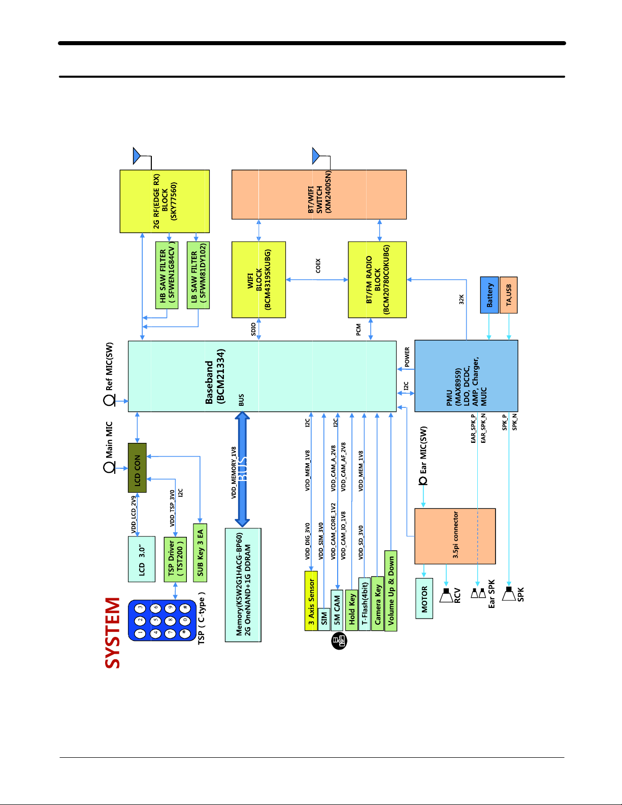
Block Diagram
8-1.
Repair
3
8-1
SAMSUNG Proprietary-Contents may change without notice
This Document can not be used without Samsung's authorization
Page 2
Level3Repair
PCB Diagrams
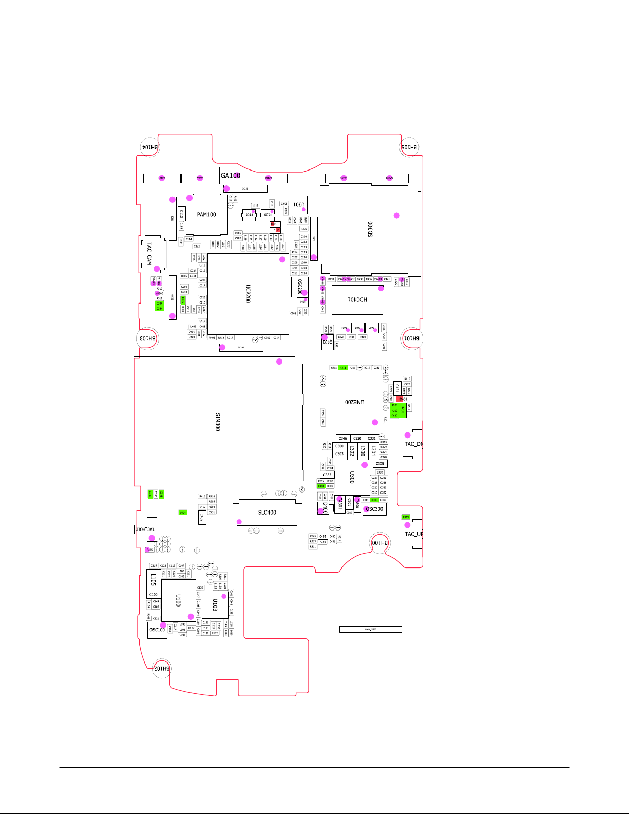
8-2.
8-2-1.
Top
(2010.12.17
Rev
0.5)
8-2
SAMSUNG Proprietary-Contents may change without notice
This Document can not be used without Samsung's authorization
Page 3
Level3Repair
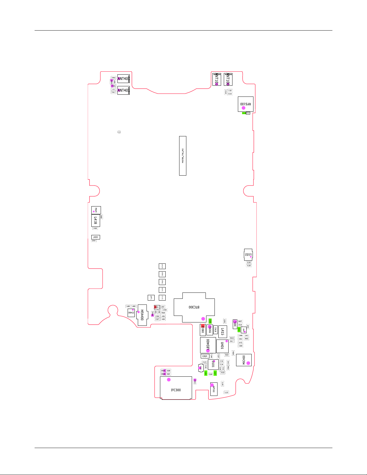
8-2-1.
Bottom
8-3
SAMSUNG Proprietary-Contents may change without notice
This Document can not be used without Samsung's authorization
Page 4
Level3Repair
Flow Chart of Troubleshooting
8-3.
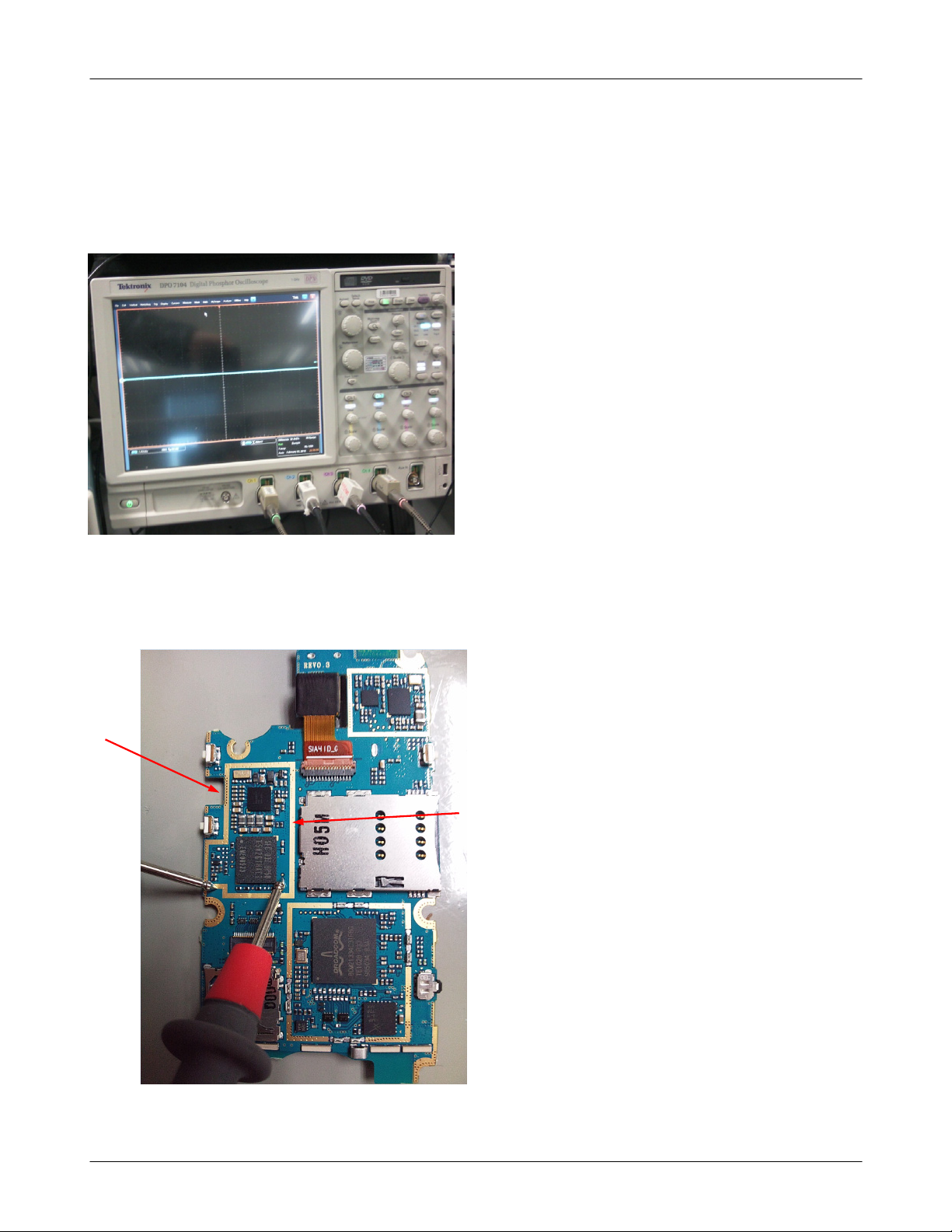
presetting methods for checking TP
※
GND&TP(exp. VBAT=
-
look over the coming out signal.
-
TA300
,
C303
using Oscilloscope
)
GND
Oscilloscope
←
TP(Test Point)
8-4
SAMSUNG Proprietary-Contents may change without notice
This Document can not be used without Samsung's authorization
Page 5
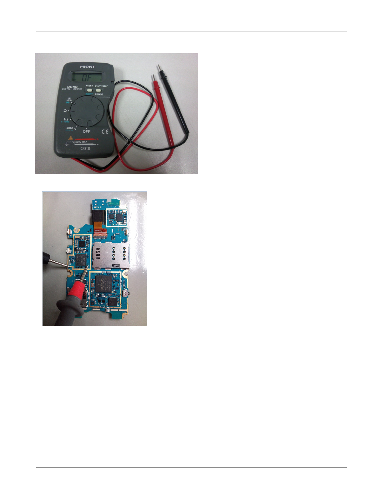
Multi-meter
←
Level3Repair
Checking the TP(test point) using Multi-meter
←
EX) to look up the TP, shunt Cap.-if checking the GND, you can listen"beep"
-
if checking the Signal, you can't listen it.
8-5
SAMSUNG Proprietary-Contents may change without notice
This Document can not be used without Samsung's authorization
Page 6
Level3Repair
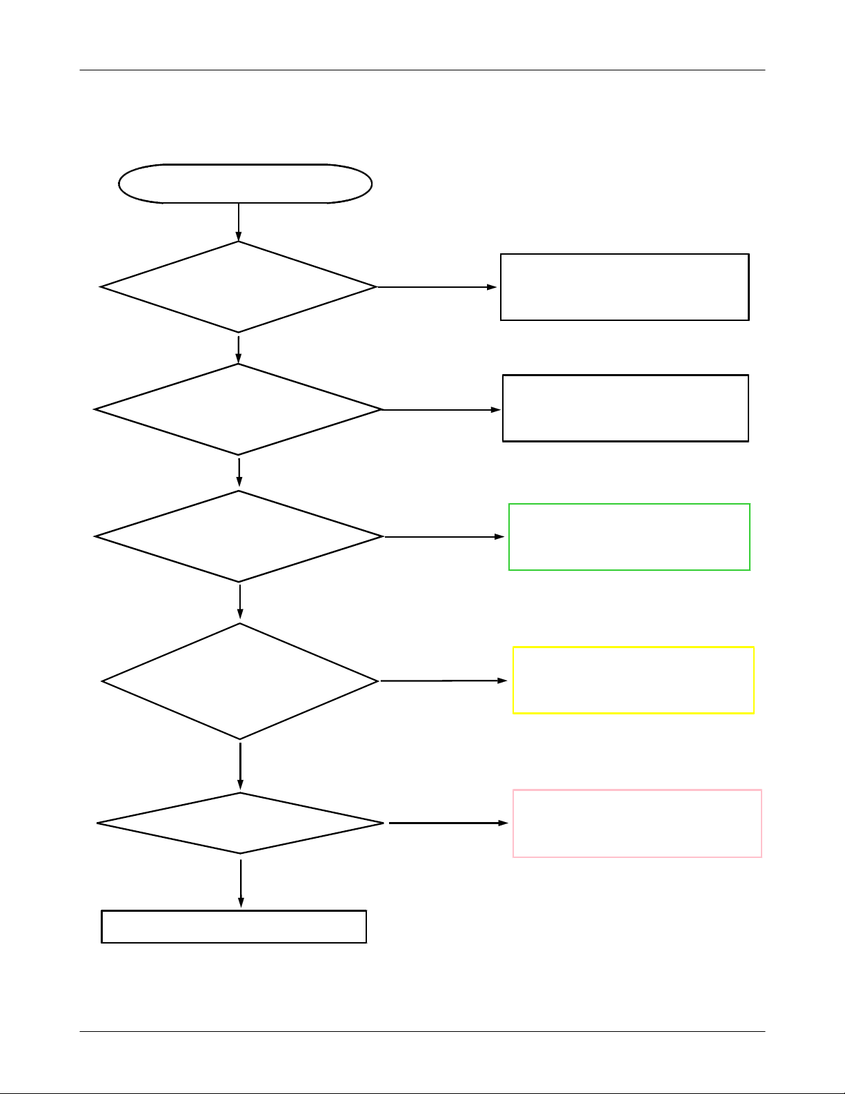
LOGIC
8-3.
8-3-1.
Power On
Power switch on
NG
Check the current
consumption
>= 100
mA?
Yes
Check the battery
voltage
>= 3.45?
Yes
Check the clock at
OSC300
=32
kHz
Yes
C220(1.28V_VCORE)=1.28V?
C211(3.0V_DIG)=3.0V?
C214(1.8V_MEM)=1.8V?
C221(2.7V_VRF)=2.7?
C224(1.3V_VRF)=1.3V?
C208(1.3V_VCXO)=1.3V?
NO
Download
NO
Change the battery
NO
?
Resolder OSC300
NO
Check the U300
Yes
Check the clock
MHz
26
?
Yes
Check the initial operation
SAMSUNG Proprietary-Contents may change without notice
This Document can not be used without Samsung's authorization
NO
Check the clock generation circuit
OSC200
8-6
Page 7
Level3Repair
VDD_ANA_3V0
VDD_CAM_A_2V8
VDD_ANA_1V2
VDD_VRF_1V3
VDD_VRF_2V7
VDD_USBOTG_2V5
VDD_LCD_2V9
VDD_USB_NVRAM_3V3
VDD_CAM_IO_1V8
VDD_CAM_AF_2V8
VDD_MOT_3V0
VDD_TSP_3V0
VDD_CORE_1V28
VDD_MEM_1V8
VDD_CAM_CORE_1V2
VDD_AMP1_3V0
VDD_SD_3V0
VDD_DIG_3V0
VDD_VCXO_1V3
VDD_SIM_3V0
LDO_EN4
SCL
SDA
C331
C330 C329C320
C346
C323
C319 723C523C
C318
C322
VBAT
VDD_MEM_1V8
C300
C303
TA300
C305
L300
L301
L302
C324
C328
C326
9
3
J
C
T
T
A
B
B1
C304
IN1
B2
IN2
C2
IN3
C5
IN4
C6
IN5
C8
IN6
D7
IN7
B3
INLV
B8
ALDO1
B7
ALDO2
C3
LVLDO1
C4
LVLDO2
A8
RFLDO1
A7
RFLDO2
B4
MSLDO1
B6
MSLDO2
F9
AUXLDO1
F8
AUXLDO2
E8
AUXLDO3
E7
AUXLDO4
E6
AUXLDO5
C1
LX1
A2
LX2
E1
LX3
D2
FB1
A3
FB2
F2
FB3
A6
HCLDO1
A5
HCLDO2
B5
IOLDO
F6
LCLDO
A4
SIMLDO
F3
I2CCLK
F4
I2CDAT
F7
EN5
E5
EN4
D
N
G
9
9
E
G
C332
VDD_MEM_1V8
1
F
D
D
D
D
V
V
P
P
H
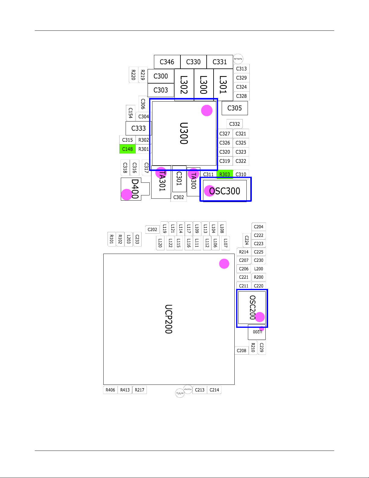
U300
D
D
N
N
G
G
1
J
VBUS_IF
C301
2
8
7
9
C302
D
C
D
G
L
D
S
IN
V
D
U
O
V
B
C
V
V
J7
COMN1
J8
COMP2
J2
C1N
H2
C1P
H9
DN1
J9
DP2
H1
OUTN
G1
OUTP
H3
INA1
F5
INB2
H7
UT1
G7
UR2
H8
UID
H6
SL1
H5
SR2
J6
HPL
J5
HPR
G3
PC1
E4
PC2
A9
XIN
B9
XOUT
G5
INB1
G4
INA2
G6
MIC
D3
IRQB
G8
BC
D4
C313
REFBP
D5
RESETB
H4
VBIAS
E3
PWRONB
D6
32KHZ
1
NC
2
NC
3
1
2
S
D
D
D
S
N
N
N
V
P
G
G
G
P
P
P
H
2
1
1
4
J
E
A
D
C333C321C317C316
TP_USB_DM
TP_USB_DP
TP_USB_TXD
TP_USB_RXD
TP_PMU_IRQ
DM_IF
DP_IF
C306
USB_DM
USB_DP
C307
PMU_IRQ
C315
RST_BB
TA301
SPK_N
SPK_P
EAR_L
AMP_N
FM_R_OUT
USB_TXD
USB_RXD
JIG_ID
R301
R302
R303
C314
EAR_SPK_L
EAR_SPK_R
PC
BT_REQ_CLK
C310
OSC300
C311
FM_L_OUT
AMP_P
EAR_R
ONKEY
32K_CLK
8-7
SAMSUNG Proprietary-Contents may change without notice
This Document can not be used without Samsung's authorization
Page 8
Level3Repair
8-8
SAMSUNG Proprietary-Contents may change without notice
This Document can not be used without Samsung's authorization
Page 9

Level3Repair
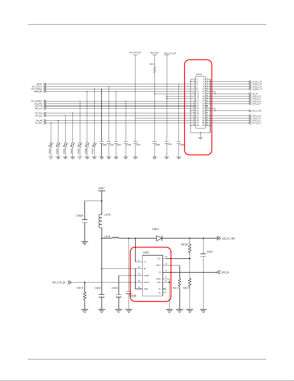
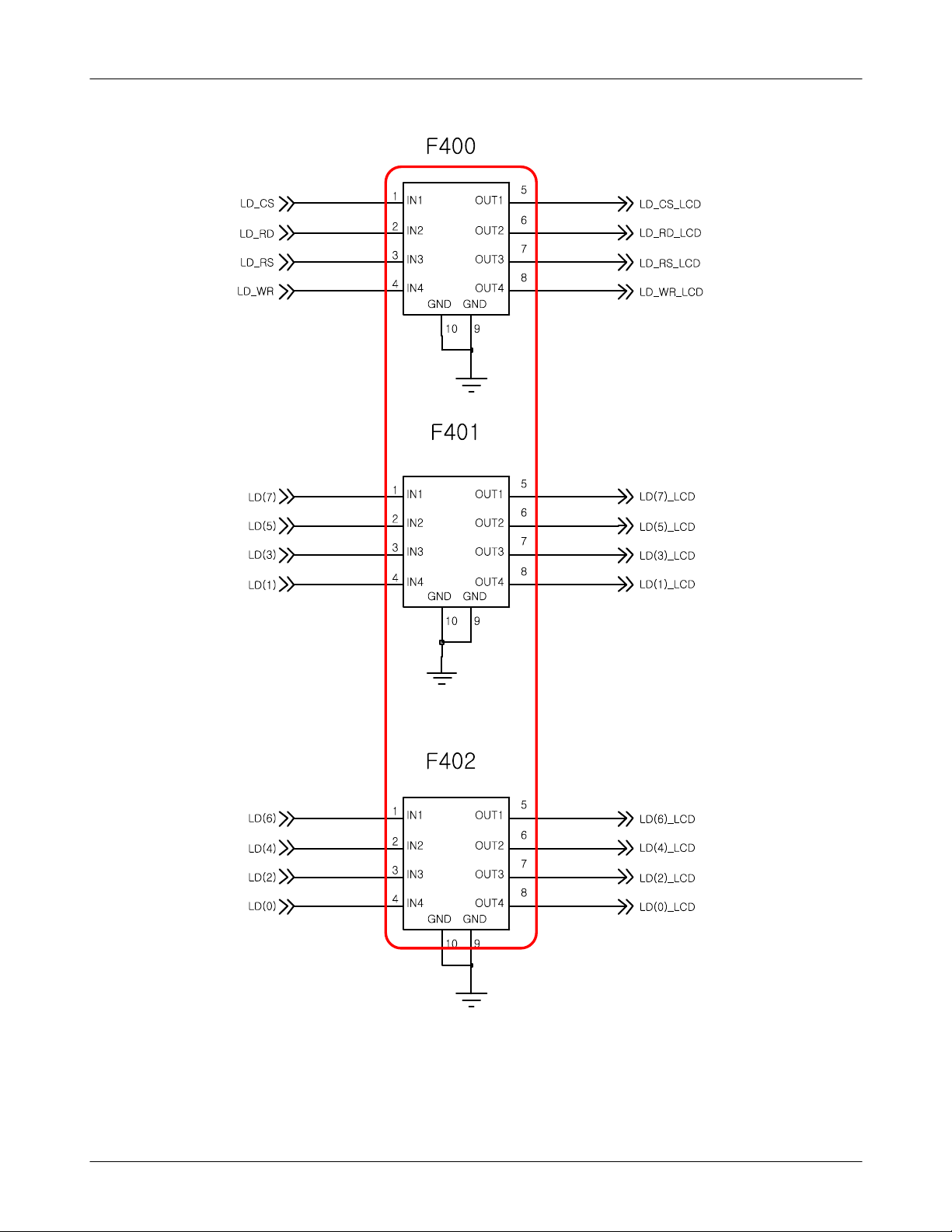
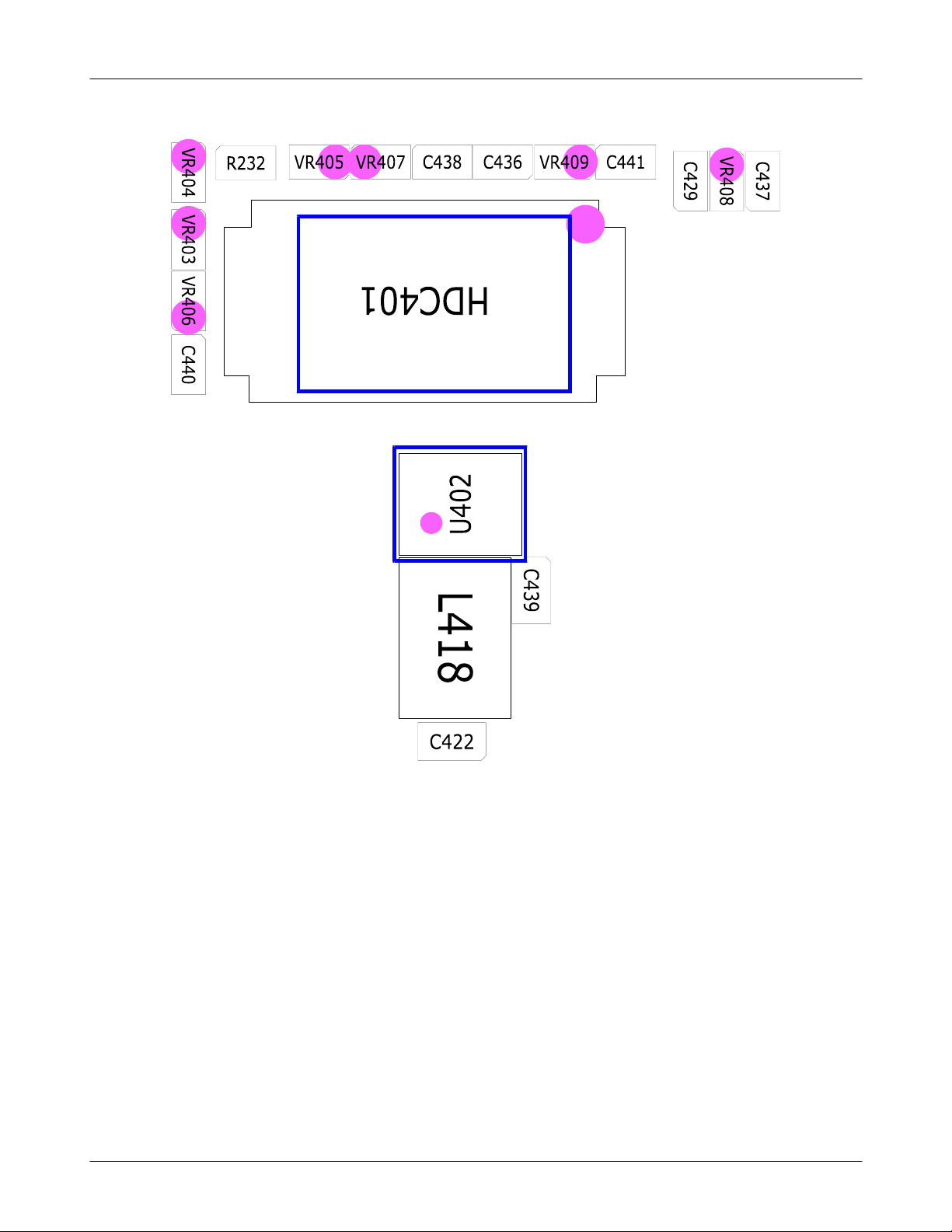
8-3-2.
LCD Working
Power Switch On
LCD Display
On?
Yes
NO
LCD FPCB
connector is co
rrectly connecti
ned?
Yes
F400, F401,
F402, HDC401
Correctly moun
ted?
NO
NO
correctly connect
F400, F401,
F402, HDC401
Resolder
,
Yes
LCD
Replace
Yes
C421
LED_P_18V=18V?
NO
Replace U402&Check
neighboring circuits
8-9
SAMSUNG Proprietary-Contents may change without notice
This Document can not be used without Samsung's authorization
Page 10
Level3Repair
8-10
SAMSUNG Proprietary-Contents may change without notice
This Document can not be used without Samsung's authorization
Page 11
Level3Repair
8-11
SAMSUNG Proprietary-Contents may change without notice
This Document can not be used without Samsung's authorization
Page 12
Level3Repair
8-12
SAMSUNG Proprietary-Contents may change without notice
This Document can not be used without Samsung's authorization
Page 13
Level3Repair
8-3-3.
TSP
Operate TSP
NG
Check
TSP Connecting
YES
Change TSP Module
No Problem? Change main PBA
NO
Reconnecting TSP
NO
YES
END
8-13
SAMSUNG Proprietary-Contents may change without notice
This Document can not be used without Samsung's authorization
Page 14

Level3Repair
8-3-4.
Audio Working
Speaker Working
Operate speaker
NG
Check
Speaker
Connecting
YES
Speaker break
down?
NO
NO
YES
Reconnecting SPK
Change Speaker
Module
Signal on in
L409, L411?
NO
Signal on in
C307, C314?
NO
Change main PBA
YES
YES
Resolder
L409,L411
Resolder
C307, C314
Replace U300
8-14
SAMSUNG Proprietary-Contents may change without notice
This Document can not be used without Samsung's authorization
Page 15

Level3Repair
8-15
SAMSUNG Proprietary-Contents may change without notice
This Document can not be used without Samsung's authorization
Page 16

Level3Repair
VDD_ANA_3V0
VDD_CAM_A_2V8
VDD_ANA_1V2
VDD_VRF_1V3
VDD_VRF_2V7
VDD_USBOTG_2V5
VDD_LCD_2V9
VDD_USB_NVRAM_3V3
VDD_CAM_IO_1V8
VDD_CAM_AF_2V8
VDD_MOT_3V0
VDD_TSP_3V0
VDD_CORE_1V28
VDD_MEM_1V8
VDD_CAM_CORE_1V2
VDD_AMP1_3V0
VDD_SD_3V0
VDD_DIG_3V0
VDD_VCXO_1V3
VDD_SIM_3V0
LDO_EN4
SCL
SDA
C330 C329C320
C346
C331
C319 723C523C
C318
C323
C322
VDD_MEM_1V8
VBAT
TA300
C303
C305
L300
L301
L302
C324
C326
C304
C328
VDD_MEM_1V8
VBUS_IF
C300
2
9
7
9
1
3
J
F
D
C
C
G
S
N
D
T
D
I
T
D
U
D
O
A
B
V
V
C
B
V
P
P
V
H
B1
IN1
B2
IN2
C2
IN3
C5
IN4
C6
IN5
C8
IN6
D7
IN7
B3
INLV
B8
ALDO1
B7
ALDO2
C3
LVLDO1
C4
LVLDO2
A8
RFLDO1
A7
RFLDO2
B4
MSLDO1
B6
MSLDO2
F9
AUXLDO1
F8
AUXLDO2
E8
AUXLDO3
E7
AUXLDO4
E6
AUXLDO5
U300
C1
LX1
A2
LX2
E1
LX3
D2
FB1
A3
FB2
F2
FB3
A6
HCLDO1
A5
HCLDO2
B5
IOLDO
F6
LCLDO
A4
SIMLDO
F3
I2CCLK
F4
I2CDAT
F7
EN5
E5
EN4
1
S
D
S
D
D
D
N
V
N
N
N
P
G
H
P
G
G
G
9
1
9
1
4
1
J
J
D
E
A
G
C332
C333C321C317C316
C301
8
C302
D
L
D
V
D
V
J7
COMN1
J8
COMP2
J2
C1N
H2
C1P
H9
DN1
J9
DP2
H1
OUTN
G1
OUTP
H3
INA1
F5
INB2
H7
UT1
G7
UR2
H8
UID
H6
SL1
H5
SR2
J6
HPL
J5
HPR
G3
PC1
E4
PC2
A9
XIN
B9
XOUT
G5
INB1
G4
INA2
G6
MIC
TP_PMU_IRQ
D3
IRQB
G8
BC
D4
C313
REFBP
D5
RESETB
H4
VBIAS
E3
PWRONB
D6
32KHZ
1
NC
2
NC
2
3
D
D
N
N
G
G
P
P
2
E
C306
TP_USB_DM
TP_USB_DP
TP_USB_TXD
TP_USB_RXD
C307
PMU_IRQ
RST_BB
DM_IF
DP_IF
USB_DM
USB_DP
C315
TA301
SPK_N
SPK_P
EAR_L
AMP_N
FM_R_OUT
USB_TXD
USB_RXD
JIG_ID
R301
R302
R303
C314
OSC300
EAR_SPK_L
EAR_SPK_R
PC
BT_REQ_CLK
C310
C311
FM_L_OUT
AMP_P
EAR_R
ONKEY
32K_CLK
8-16
SAMSUNG Proprietary-Contents may change without notice
This Document can not be used without Samsung's authorization
Page 17

Receiver Working
Operate Receiver
Level3Repair
NG
Check
Receiver
Connecting
YES
Receiver break
down?
NO
Change main PBA
NO
YES
Reconnecting
Change Receiver
Module
8-17
SAMSUNG Proprietary-Contents may change without notice
This Document can not be used without Samsung's authorization
Page 18

Level3Repair
MainMICWorking
Operate MIC
NG
Pollute
MIC Hole?
NO
Check
C437=High?
YES
Change MIC
NO
YES
Clean up
MIC hole
Remove MIC,
Check C440 pin
High
?
YES
Change MIC
NO
Check R405 High?
NO YES
Change PBA Change MIC_SWITCH
8-18
SAMSUNG Proprietary-Contents may change without notice
This Document can not be used without Samsung's authorization
Page 19

Level3Repair
8-19
SAMSUNG Proprietary-Contents may change without notice
This Document can not be used without Samsung's authorization
Page 20

Level3Repair
Stereo Headset Working
Hands-free stereo
headset
NG
YES
Chang Hands-free headsetButton NG?
NO
MIC NG?
NO
SPK NG?
NO
The End
YES
YES
Check
L405
YES
Resolder L405
Signal on
in C406,
C407?
NO
Signal on
in C307
C314?
NO
YES
YES
NO
Check HEA400
Check L406, L408,
HEA400
Check R301, R302,
U300
Change Main PBA
8-20
SAMSUNG Proprietary-Contents may change without notice
This Document can not be used without Samsung's authorization
Page 21

Level3Repair
VDD_ANA_3V0
VDD_CAM_A_2V8
VDD_ANA_1V2
VDD_VRF_1V3
VDD_VRF_2V7
VDD_USBOTG_2V5
VDD_LCD_2V9
VDD_USB_NVRAM_3V3
VDD_CAM_IO_1V8
VDD_CAM_AF_2V8
VDD_MOT_3V0
VDD_TSP_3V0
VDD_CORE_1V28
VDD_MEM_1V8
VDD_CAM_CORE_1V2
VDD_AMP1_3V0
VDD_SD_3V0
VDD_DIG_3V0
VDD_VCXO_1V3
VDD_SIM_3V0
LDO_EN4
SCL
SDA
C330 C329C320
C346
C331
C319 723C523C
C318
C323
C322
VDD_MEM_1V8
VBAT
TA300
C303
C305
L300
L301
L302
C324
C326
C304
C328
VDD_MEM_1V8
VBUS_IF
C300
9
7
9
1
3
J
F
D
C
C
S
N
D
T
D
I
T
D
U
D
O
A
B
V
V
C
B
V
P
P
V
H
B1
IN1
B2
IN2
C2
IN3
C5
IN4
C6
IN5
C8
IN6
D7
IN7
B3
INLV
B8
ALDO1
B7
ALDO2
C3
LVLDO1
C4
LVLDO2
A8
RFLDO1
A7
RFLDO2
B4
MSLDO1
B6
MSLDO2
F9
AUXLDO1
F8
AUXLDO2
E8
AUXLDO3
E7
AUXLDO4
E6
AUXLDO5
U300
C1
LX1
A2
LX2
E1
LX3
D2
FB1
A3
FB2
F2
FB3
A6
HCLDO1
A5
HCLDO2
B5
IOLDO
F6
LCLDO
A4
SIMLDO
F3
I2CCLK
F4
I2CDAT
F7
EN5
E5
EN4
1
S
D
S
D
D
D
N
V
N
N
N
P
G
H
P
G
G
G
9
1
9
4
1
J
J
D
E
G
C332
C333C321C317C316
C301
2
8
C302
D
G
L
D
V
D
V
J7
COMN1
J8
COMP2
J2
C1N
H2
C1P
H9
DN1
J9
DP2
H1
OUTN
G1
OUTP
H3
INA1
F5
INB2
H7
UT1
G7
UR2
H8
UID
H6
SL1
H5
SR2
J6
HPL
J5
HPR
G3
PC1
E4
PC2
A9
XIN
B9
XOUT
G5
INB1
G4
INA2
G6
MIC
TP_PMU_IRQ
D3
IRQB
G8
BC
D4
C313
REFBP
D5
RESETB
H4
VBIAS
E3
PWRONB
D6
32KHZ
1
NC
2
NC
3
2
D
D
N
N
G
G
P
P
2
1
E
A
C306
TP_USB_DM
TP_USB_DP
TP_USB_TXD
TP_USB_RXD
C307
PMU_IRQ
RST_BB
C315
DM_IF
DP_IF
USB_DM
USB_DP
TA301
SPK_N
SPK_P
EAR_L
AMP_N
FM_R_OUT
USB_TXD
USB_RXD
JIG_ID
R301
R302
R303
C314
OSC300
EAR_SPK_L
EAR_SPK_R
PC
BT_REQ_CLK
C310
C311
FM_L_OUT
AMP_P
EAR_R
ONKEY
32K_CLK
8-21
SAMSUNG Proprietary-Contents may change without notice
This Document can not be used without Samsung's authorization
Page 22

Level3Repair
8-22
SAMSUNG Proprietary-Contents may change without notice
This Document can not be used without Samsung's authorization
Page 23

Level3Repair
8-3-5.
KEY Working
Volume KEY
Press Volume Key
All key NG?
Change TAP
NG
YES
Change Key TAP
NO
Any key NG?
NO
END
YES
Change Main PBA
8-23
SAMSUNG Proprietary-Contents may change without notice
This Document can not be used without Samsung's authorization
Page 24

Level3Repair
Main Key
Press Power Key
Power(END)
Key NG?
NO
Yes
key PBA FPCB
3
Connector
correct
ly connectined?
NO
Correctly connect
Yes
Change Key PBA
Change Main PBA
The End
8-24
SAMSUNG Proprietary-Contents may change without notice
This Document can not be used without Samsung's authorization
Page 25

Level3Repair
8-3-6.
Vibrator Working
Operate Vibrator
Check
Vibrator connector
3.0
C317)
(
NO
Yes
V_VIB
=3.0V?
NO
No
Reconnecting
Check PMIC(U300)
Change Main PBA/ Motor
Yes
D400
C435
=3.0
V?
NO
Change Main PBA
Yes
Resolder C435
8-25
SAMSUNG Proprietary-Contents may change without notice
This Document can not be used without Samsung's authorization
Page 26

Level3Repair
8-3-7.
T-Flash Card Working
Insert&Operate
microSD card
break down
th Pin of SD300
12
SD300
High
=
NG
NO
YES
?
Change SD300
YES
?
Change SD300
NO
th Pin of SD300
4
=3.0V?
YES
Change Main PBA
NO
Check U300(PMIC)
8-26
SAMSUNG Proprietary-Contents may change without notice
This Document can not be used without Samsung's authorization
Page 27

Level3Repair
8-27
SAMSUNG Proprietary-Contents may change without notice
This Document can not be used without Samsung's authorization
Page 28

Level3Repair
8-3-8.
SIM Card Working
Insert&Operate
SIM card
NG
SIM Soket
Break down?
No
R304
=2.9V
Yes
No
Change SIM Soket
Check PMIC
U300)
(
Yes
Change PBA
8-28
SAMSUNG Proprietary-Contents may change without notice
This Document can not be used without Samsung's authorization
Page 29

Level3Repair
8-29
SAMSUNG Proprietary-Contents may change without notice
This Document can not be used without Samsung's authorization
Page 30

Level3Repair
8-3-9
CAMERA Working
Operate CAMERA
NG
Camera FPCB con
nector is correctly
connected?
Yes
C432/C323
C431
C433
=2.8
=1.8V
=2.8V
V,
NO
NO
correctly connect
Change
U300(PMIC)/PBA
Yes
CAMERA
Replace
8-30
SAMSUNG Proprietary-Contents may change without notice
This Document can not be used without Samsung's authorization
Page 31

Level3Repair
8-31
SAMSUNG Proprietary-Contents may change without notice
This Document can not be used without Samsung's authorization
Page 32

Level3Repair
presetting
※
Rx setting)
(
Active Cell
1.
select GSM or GPRS
:
Connetion Type
2.
select Auto(GSM), BLER(GPRS)
:
BCH Parameter
3.
select measuring band(DCS or EGSM)
:
Cell power
4.
dBm
:-60
8960
8-32
SAMSUNG Proprietary-Contents may change without notice
This Document can not be used without Samsung's authorization
Page 33

Tx setting)
(
After setting
※
After setting, prepare the call setup Display
1.
UsinganOriginateCall,makeacall.
2.
Confirm the display"connected"
3.
start the measuring
4.
8960 (
EGSM/DCS
)
Level3Repair
※
8960 &
spectrum analyzer
down&up at picture)
(
spectrum analyzer:testing method=the way using an Osciliscope
-
-8960:
r
connect using RF Cable between
SAMSUNG Proprietary-Contents may change without notice
This Document can not be used without Samsung's authorization
8960 &
RF Connector in board.
8-33
Page 34

Level3Repair
8-3-10.
GSM
Cell Power
PAM100
L103 using spectrum
(
PAM100 Pin18
D100,D101,L104,L106,L
850
RX ON
-65
analyzer)
-68
F100
L108
107,
75
-
Receiver
dBm
:-60
Yes
Pin
11
≥
dBm
Yes
≥
dBm
Yes
pin,
8,9
≥
dBm
No
No
Resolder PAM100, L103,C114
Check PAM100
No
Resolder F100,D100,D101,L104,L106,L107,L108
control check
No
Yes
Check ANT Switch
control circuit
Resolder PAM100
Yes
Check UCP200
Yes
END
8-34
SAMSUNG Proprietary-Contents may change without notice
This Document can not be used without Samsung's authorization
Page 35

Level3Repair
8-3-11.
GSM
Cell Power
PAM100
L103 using spectrum
(
PAM100 Pin18
L109,L111,L112,L113
900
RX ON
dBm
-65
analyzer)
dBm
-68
F100
75
-
Receiver
:-60
Yes
Pin
01
Yes
Yes
Pin,
6,7
dBm
dBm
≥
≥
≥
No
No
Resolder PAM100, L103,C114
Check PAM100
control check
No
Resolder F100
No
Yes
pin, L109,L111,L112,L113
6,7
Check ANT Switch
control circuit
Resolder PAM100
Yes
Check UCP20
Yes
END
0
8-35
SAMSUNG Proprietary-Contents may change without notice
This Document can not be used without Samsung's authorization
Page 36

Level3Repair
8-3-12.
DCS Receiver
RX ON
Cell Power
PAM100
L103 using spectrum
(
PAM100 Pin
L114,L115,L116,L117
-65
analyzer)
-68
F101
75
-
Pin
dBm
dBm
9,8
≥
dBm
:-60
Yes
11
Yes
16≥
Yes
pin,
dBm
≥
No
No
No
Resolder PAM100, L103,C114
Check PAM100
control check
Resolder F101
pin, L114, L115, L116, L117
8,9
No
Yes
Check ANT Switch
control circuit
Resolder PAM100
Yes
Check UCP20
Yes
END
0
8-36
SAMSUNG Proprietary-Contents may change without notice
This Document can not be used without Samsung's authorization
Page 37

Level3Repair
8-3-13.
PCS Receiver
RX ON
Cell Power
PAM100
L103 using spectrum
(
PAM100 Pin16
L119,L120,L121,L122
-65
analyzer)
-68
F101
75
-
Pin
dBm
dBm
6,7
≥
dBm
:-60
Yes
11
Yes
Yes
pin,
dBm
≥
≥
No
No
No
Resolder PAM100, L103,C114
Check PAM100
control check
Resolder F101
pin, L119, L120, L121, L122
6,7
No
Yes
Check ANT Switch
control circuit
Resolder PAM100
Yes
Check UCP20
Yes
END
0
8-37
SAMSUNG Proprietary-Contents may change without notice
This Document can not be used without Samsung's authorization
Page 38

Level3Repair
Service Schematics
8-4.
8-38
SAMSUNG Proprietary-Contents may change without notice
This Document can not be used without Samsung's authorization
Page 39

Level3Repair
8-3-14.
GSM
GSM900 Transmitter
850/
TX Power is too Low!!
26
PAM100 pin
R102 using spectrum
(
Check the Voltage
C113,C155
TX ON(5Level)
CLOCK CHECK?
MHz@OSC200
YES
28≥-4
dBm
analyzer)
YES
<3.3
V?
NO
NO
NO
solder OSC200
Re-
solder or change
Re-
UCP200
Check the UCP200&VBAT
circuit.
YES
30
Pin
dBm
11
≥
PAM100
L103 using spectrum
(
analyzer)
YES
Check the RFS100
connection with PCB?
YES
Antenna
re-solder or change
NO
NO
Resolder PAM100
Resolder RFS100.
8-39
SAMSUNG Proprietary-Contents may change without notice
This Document can not be used without Samsung's authorization
Page 40

Level3Repair
8-3-15.
DCS/PCS Transmitter
TX Power is too Low!!
TX ON(5Level)
CLOCK CHECK?
26
PAM100 pin
R101 using spectrum
(
Check the Voltage
C113, C155
MHz@OSC200
YES
27≥-4
dBm
analyzer)
YES
<3.3
V?
NO
NO
NO
solder OSC200
Re-
solder or change
Re-
UCP200
Check the UCP200&VBAT
circuit.
YES
30
Pin
dBm
11
≥
PAM100
L103 using spectrum
(
analyzer)
YES
Check the RFS100
connection with PCB?
YES
Antenna
re-solder or change
NO
Resolder PAM100
NO
Resolder RFS100.
8-40
SAMSUNG Proprietary-Contents may change without notice
This Document can not be used without Samsung's authorization
Page 41

Service Schematics
8-4.
Level3Repair
8-41
SAMSUNG Proprietary-Contents may change without notice
This Document can not be used without Samsung's authorization
Page 42

Level3Repair
NC Point(Top View)
-
NC
:
U300
123456789
A
○○○○○○○○○
B
○○○○○○○○○
C
○○○○○○○○○
D
○○○○○○○○○
E
○○○○○○○○○
F
○○○○○○○○○
G
○○○○○○○○○
H
○○○○○○○○○
J
○○○○○○○○○
UME200
8-42
SAMSUNG Proprietary-Contents may change without notice
This Document can not be used without Samsung's authorization
Page 43

UCP200
1 2 3 4 5 6 7 8 9 10 11 12 13 14 15 16 17 18 19 20 21 22 23
A
○○●●○○○○○○○○○○○○○○○○○○○
B
○○○○○○○○○○○○○○○○○○○○○○○
C
○○ ○○
D
○○ ○○○○○○○○○○○○○○○○○ ○○
E
○○ ○○○○○○○○○○○○○○○○○ ○○
F
○○ ○○○○●○○○○○○○○○○○○ ○○
G
○○ ○○○○○○○○○○○○○○○○○ ○○
H
○○ ○○○○○○○○○○○ ○○○○ ○○
J
○○ ○○○○ ○○○○ ○○
K
○○ ○○○○ ○○○○ ○○
L
○○ ○○○○ ○○○○○ ○○○○ ○○
M
○○ ○○○ ○○○○○ ○○○○ ○○
N
○○ ○○○○ ○○○○○ ○○○○ ○○
P
○○ ○○○○ ○○○○○ ○○○○ ○○
R
○○ ○○○○ ○○○○ ○○
T
○○●○○○○ ○○○○ ○○
U
○○ ○○○○○○○○○○○○○○○○○ ○○
V
○○ ○○○○○○○○○○○○○○○○○ ○○
W
○● ○○○○○○○○○○○○○○○○○ ○○
Y
○● ○○○○○○○○○○○○○○○○○ ○○
AA
○○○ ○○○○
AB
○○○○○○○○○○○○○○○○●○○○○○○
AC
○○○○○○○○○○○○○○○○●○○○○○○
Level3Repair
8-43
SAMSUNG Proprietary-Contents may change without notice
This Document can not be used without Samsung's authorization
 Loading...