

Page 1
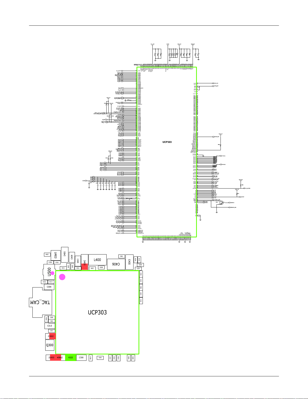
9. Flow Chart of Troubleshooting
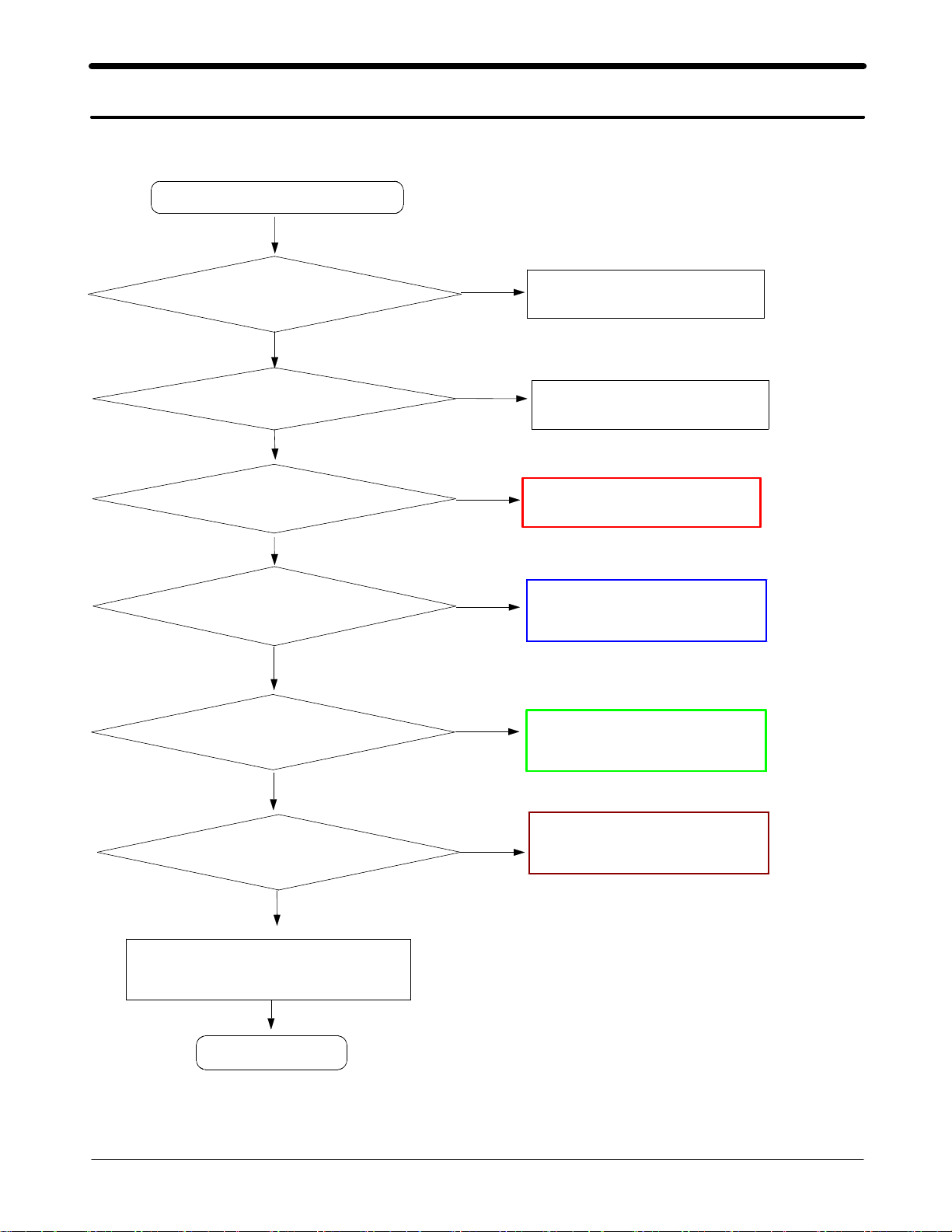
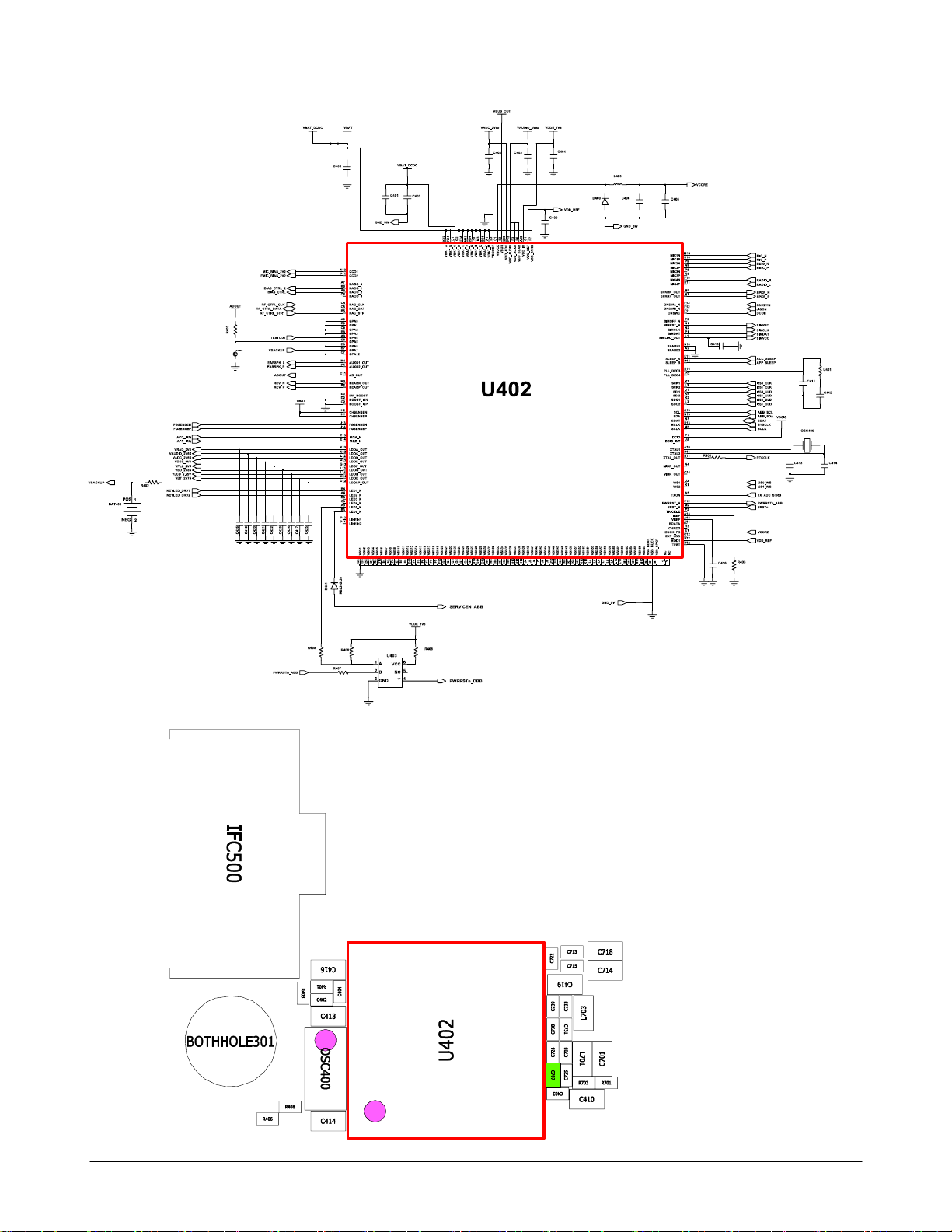
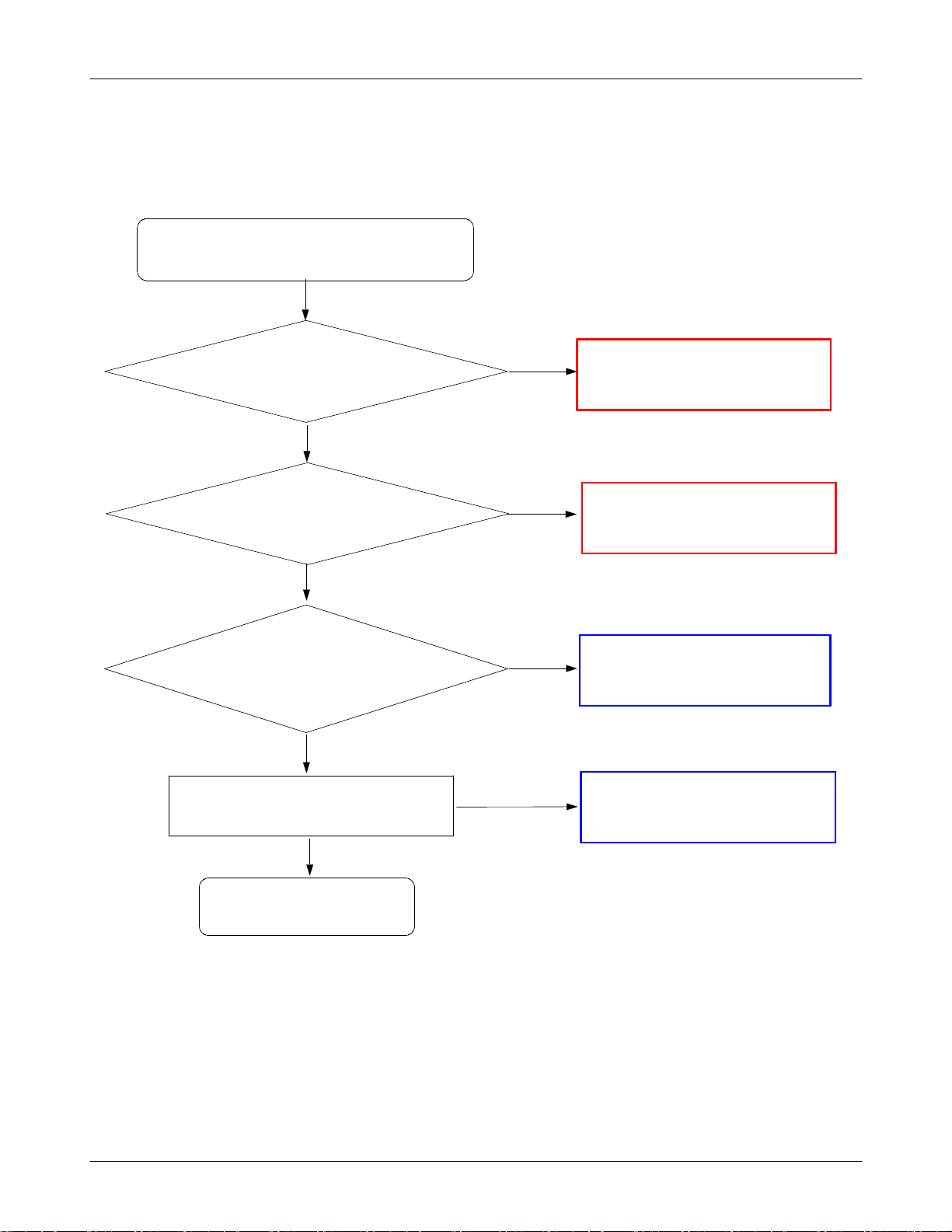
9-1.
Power On
Power On'does not work
'
Check the current consumption
more than
Check the VBAT
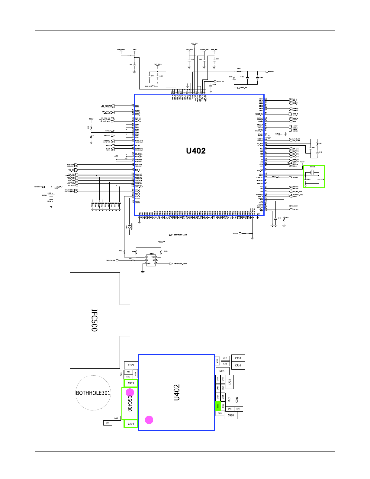
DC Resistance,solder
VDDE C421=1.8V
VADC C420=2.65V
VRAD C418=2.8
more than
Check D600
Yes
100
Yes
Yes
Yes
3.3V
mA
V?
No
Download again
No
Check the Battery
①
No
Resolder D600
②
?
?
No
Replace U402
Yes
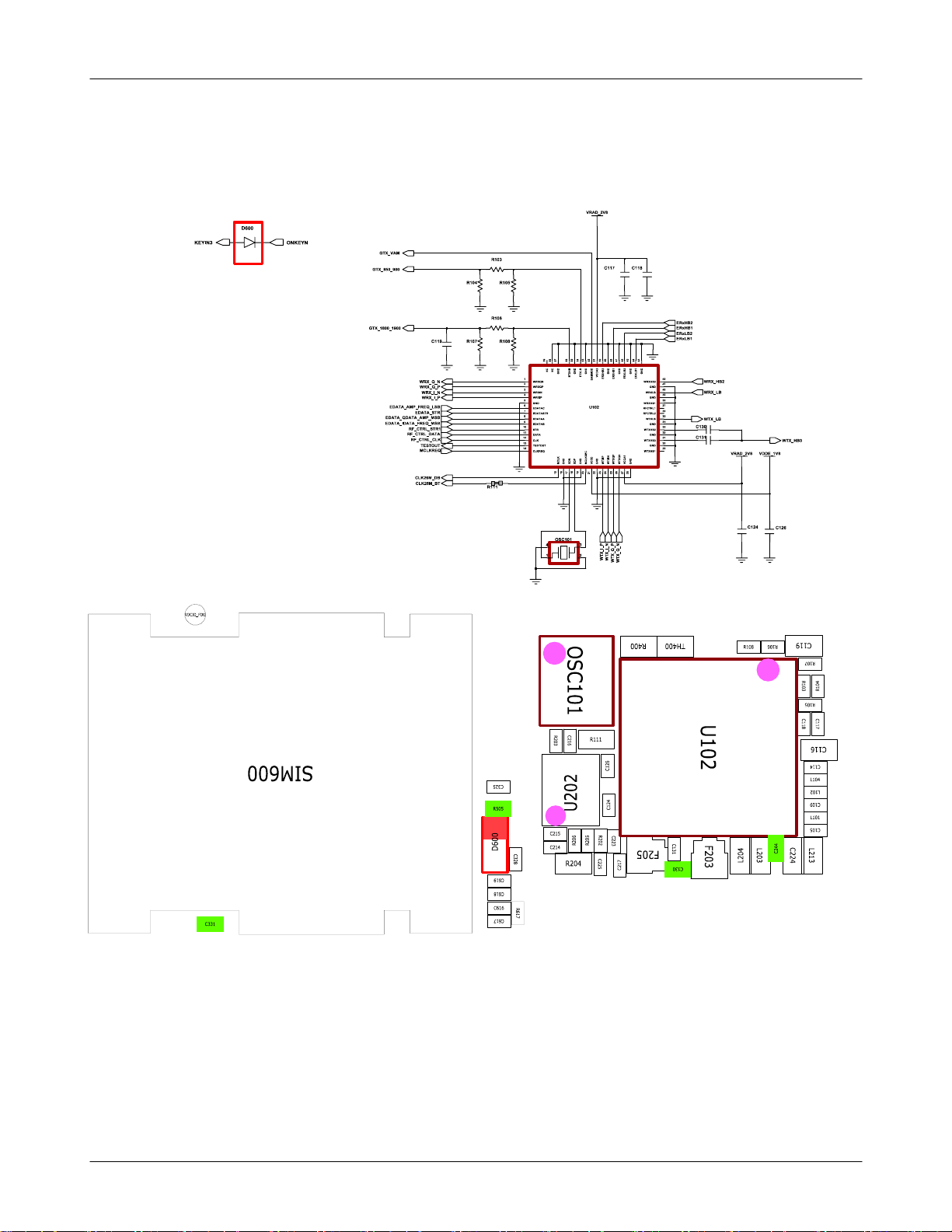
Check CLK32K
R401
Check the pin
Check the pin#1of OSC101
Check the initial operation
=32
END
Yes
#15
Yes
Yes
KHz
of U102
No
No
③
Check the clock
OSC400,C413,C414
④
Check the U102,OSC101
9-1
SAMSUNG Proprietary-Contents may change without notice
This Document can not be used without Samsung's authorization
Page 2
Flow Chart of Troubleshooting
9-2
SAMSUNG Proprietary-Contents may change without notice
This Document can not be used without Samsung's authorization
Page 3
Flow Chart of Troubleshooting
9-3
SAMSUNG Proprietary-Contents may change without notice
This Document can not be used without Samsung's authorization
Page 4
Flow Chart of Troubleshooting
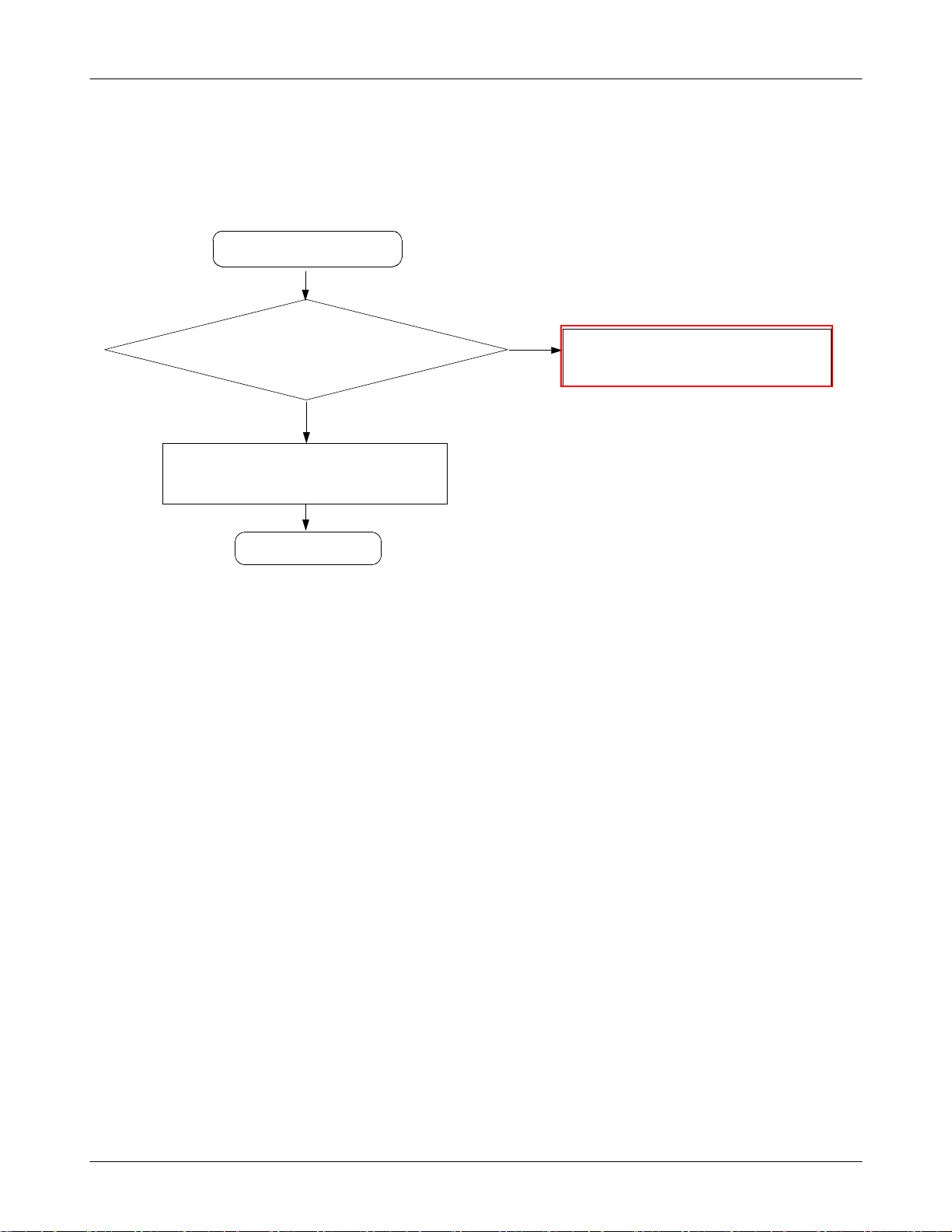
9-2.
Initial
Initial Failure
Yes
U402 pin M2(RESET/
check the test point)
(
Check the16bit data signal
memory CE
&
END
)="
Yes
Yes
H"?
No
①
Check the circuit related to reset
If it has some problem, replace it)
(
U402
9-4
SAMSUNG Proprietary-Contents may change without notice
This Document can not be used without Samsung's authorization
Page 5
Flow Chart of Troubleshooting
9-5
SAMSUNG Proprietary-Contents may change without notice
This Document can not be used without Samsung's authorization
Page 6
Flow Chart of Troubleshooting
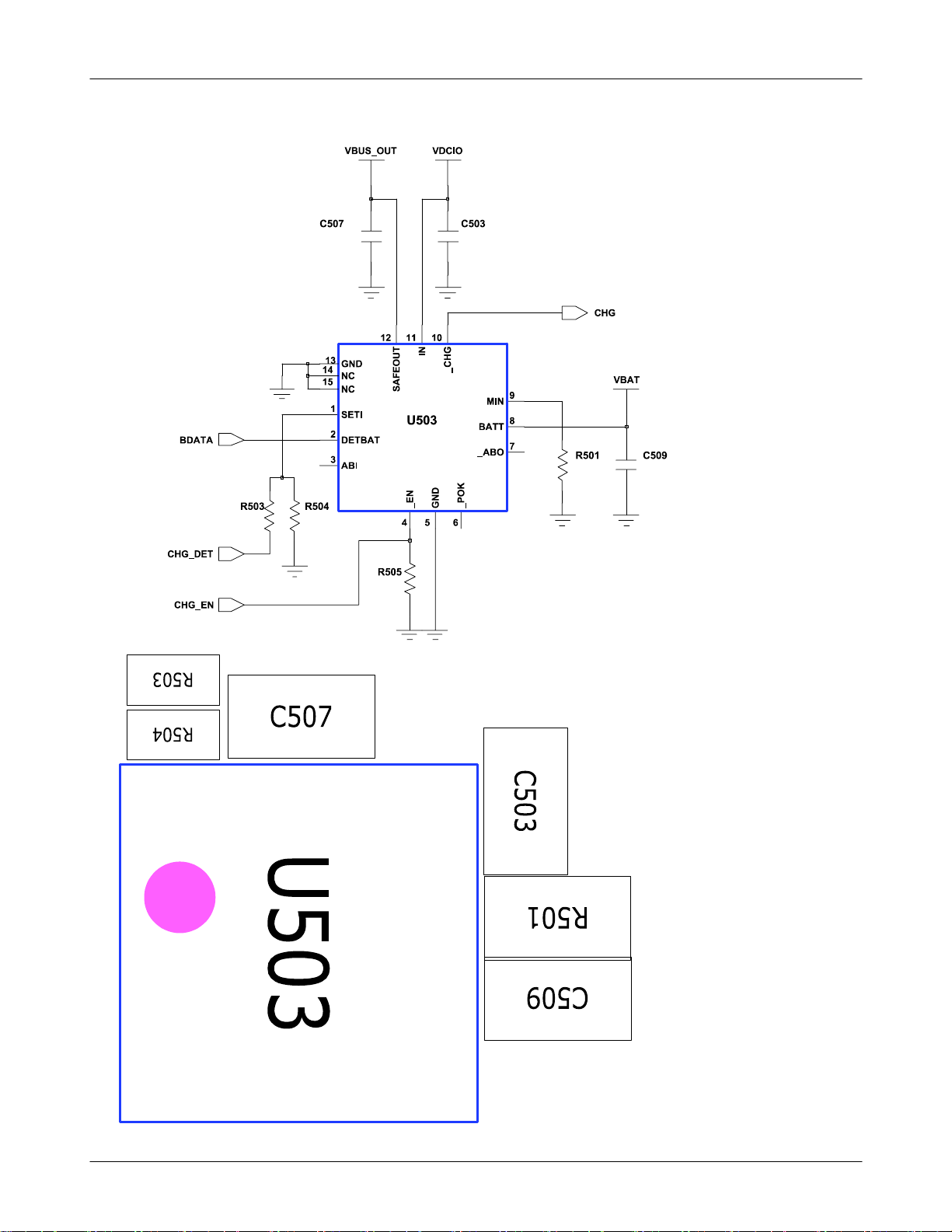
9-3.
Charging Part
Abnormal charging part
Check the pin#11(>4.5V) and
pin#2(=low) of the U503
Check the pin#10(=low) of the
U503
Yes
No
check the TA and battery connection.
Yes
①
No
Replace the U503
Yes
②
Check the pin#4(=low) of the
U503
Yes
END
No
Replace the UCP303
9-6
SAMSUNG Proprietary-Contents may change without notice
This Document can not be used without Samsung's authorization
Page 7
Flow Chart of Troubleshooting
9-7
SAMSUNG Proprietary-Contents may change without notice
This Document can not be used without Samsung's authorization
Page 8
Flow Chart of Troubleshooting
9-8
SAMSUNG Proprietary-Contents may change without notice
This Document can not be used without Samsung's authorization
Page 9
Flow Chart of Troubleshooting
9-4.
Sim Part
Check the SIMVCC R617
Phone can't access SIM Card
Yes
=3.0V
Check the SIMCLK C619
Is thereaclk
?
Yes
No
No
①
Check U402, R617
if it has some problems, replace it)
(
Check C619,U402
if it has some problems, replace it)
(
Check the SIM connector's
connector's to SIM card
Yes
Check the circuit around SIM600
input circuitry
Yes
END
②
No
resolder or change SIM600
No
Check the related circuit of SIM600
9-9
SAMSUNG Proprietary-Contents may change without notice
This Document can not be used without Samsung's authorization
Page 10
Flow Chart of Troubleshooting
9-10
SAMSUNG Proprietary-Contents may change without notice
This Document can not be used without Samsung's authorization
Page 11
Flow Chart of Troubleshooting
9-5.
Microphone Part
Microphone does not work
Check the connection
from MIC
Check the MIC_BIAS_2V2
at L702, C743=
Yes
2.2V ?
Yes
No
No
①
②
Resolder MIC
Check L702,C743,U402
If it has problem, replace it)
(
MIC700
POWER
POWER
GND2GND1
GND2GND
OUT
OUT
Check L703,C731,C733
connection
No
Resolder L703,C731,C733
Yes
END
MIC_BIAS_2V2
2
0
7
L
8
3
7
1
3
4
L703
3
4
7
C
C731
C733
C
MIC_N
MIC_P
9
3
7
C
9-11
SAMSUNG Proprietary-Contents may change without notice
This Document can not be used without Samsung's authorization
Page 12

Flow Chart of Troubleshooting
9-12
SAMSUNG Proprietary-Contents may change without notice
This Document can not be used without Samsung's authorization
Page 13

Flow Chart of Troubleshooting
9-6.
Speaker Part(Melody)
Speaker does not work
Is the terminal of speake
Is there any signal at
Check the
Pin
#5,#7
C713,C715
OK?
HIGH"
"
Yes
of HEA1
Yes
?
No
r
check the specker
①
No
Resolder U701
②
No
Check C713,C715
If it has problem replace it)
(
Yes
Is speaker OK?
Yes
END
No
Change speaker
9-13
SAMSUNG Proprietary-Contents may change without notice
This Document can not be used without Samsung's authorization
Page 14

Flow Chart of Troubleshooting
A
SPK_P
SPK_N
VAUDIO_2V65
VAUDIO_2V65
C712
C727
EAR_L
EAR_R
C714
C718
B3
B2
A3
A2
F2
F1
E4
E5
E3
F3
EARSPK_L
EARSPK_R SPKR_P
RADIO_L
RADIO_R
C742
C741
VBAT
C710
1
5
4
F
E
B
D
D
D
D
D
D
V
V
V
P
A
P
S
H
LIN1
LIN2
RIN1
RIN2
U701
HPOUTL
HPOUTR
SPOUT+
SPOUT-
RECV+
RECV-
D
D
D
D
N
N
N
N
G
G
G
C
P
G
P
D
N
A
S
C
4
1
1
5
1
A
F
C
C
C713
A4
MIN+
B4
C715
MIN-
C705
C2
CP+
D2
CP-
C717
D1
REFCP
E2
REFHP
C3
_RST
D3
CAP
D5
SCL
C5
SDA
A5
VREF
B1
VREG
D4
PROTN
C
N
2
C721
SPKR_N
MP_RST
AMP_SCL
AMP_SDA
C722
9-14
SAMSUNG Proprietary-Contents may change without notice
This Document can not be used without Samsung's authorization
Page 15

Receiver Part
9-7
Receiver does not work
Is the terminal of Receiver
Is there any signal at
OK?
C100,C101
Yes
?
No
No
Flow Chart of Troubleshooting
check the Receiver
①
Check C100,C101,U402
If it has problem, replace it)
(
Yes
Is receiver OK?
Yes
END
No
Change Receiver module
9-15
SAMSUNG Proprietary-Contents may change without notice
This Document can not be used without Samsung's authorization
Page 16

Flow Chart of Troubleshooting
VDD_CAM_1V8_IO VDD_CAM_1V8_CORE
R100
0ohm
1005
SHORT
CAM_SDA
CAM_V_SYNC
CAM_H_SYNC
CAM_CIF_RST
CAM_D(7)
CAM_D(6)
CAM_D(5)
CAM_D(4)
CAM_D(3)
HEA100
14-5802-024-002-829
1
2
1
4
3
3
56
5
8
7
7
9
10
9
12
11
11
14
13
13
16
15
15
18
17
17
19
20
19
22
21
21
23
24
23 24
NC
NC
NC
NC
27
28
2526
VDD_CAM_1V8_IO
2
4
6
8
10
12
14
16
18
20
22
F
n
0
0
5
0
2
0
2
1
2
6.3V
0
1
C
VDD_CAM_1V8_CORE
VDD_CAM_2V8_AVDD
F
n
0
0
5
0
2
0
2
1
3
6.3V
6.3V
0
1
C
R108
10
1005
R109
CAM_SCL
CAM_MCLK
CAM_PCLK
CAM_SUB_STANDBY
CAM_D(0)
CAM_D(1)
CAM_D(2)
F
n
0
0
5
5
2
0
0
2
0
0
1
1
4
50V
0
1
C
F
F
5
0
N
N
0
1
1
1
1
0
50V
0
0
1
1
C
C
RCVP
10
RCVN
1005
9-16
SAMSUNG Proprietary-Contents may change without notice
This Document can not be used without Samsung's authorization
Page 17

Flow Chart of Troubleshooting
9-8.
Key Data Input
Check Initial Operation
When one of the keys is
pushed,
does it works physically?
When one of the keys is
pushed,
is it displayed on the LCD?
Yes
Yes
No
No
Check the Dome sheet,Volume KeyFPCB
Check the Dome sheet, Volume KeyFPCB
Key Pad
HDC
601.
&
END
Yes
9-17
SAMSUNG Proprietary-Contents may change without notice
This Document can not be used without Samsung's authorization
Page 18

Flow Chart of Troubleshooting
9-18
SAMSUNG Proprietary-Contents may change without notice
This Document can not be used without Samsung's authorization
Page 19

Flow Chart of Troubleshooting
9-9.
Camera part
Camera" function does not work
"
Is there another problem?
Yes
Check the Camera
connector on PBA
Yes
Yes
Replace the camera
module
①
No
Check the con HDC602
If there is no problem
Reconnect the camera module
CAM_PCLK
CAM_H_SYNC
CAM_V_SYNC
CAM_D(7)
CAM_D(6)
CAM_D(5)
CAM_D(4)
CAM_D(3)
CAM_D(2)
CAM_D(1)
CAM_D(0)
C621
L600
1005
END
HDC602
11
3344
5
5
77 8
99
11 11 12
1313
15 15 16
1717
19 192220
2121
C
C
C
N
N
N
3
5
4
2
2
2
VDD_CAM_1V8_CORE
VDD_CAM_1V8_IO
6
6
8
10
10
12
14
14
16
18
18
20
22
22
C
N
6
2
VDD_CAM_2V8_AVDD
CAM_MCLK
CAM_MAIN_RST
CAM_MAIN_STANDBY
VDD_CAM_1V8_IO
R604R603
CAM_SCL
CAM_SDA
9-19
SAMSUNG Proprietary-Contents may change without notice
This Document can not be used without Samsung's authorization
Page 20

Flow Chart of Troubleshooting
9-10.
Radio part
Radio does not work
Is there any signal at
C238
=1.8V?
C231,C237
Yes
Yes
Yes
?
No
No
No
①
Resolder C238
and Check U402
②
Check the U206
if it has problem,replace it)
(
③
Is there any signal at
L504,L505
Is there any signal at
ZD502,ZD503
END
?
Yes
?
Yes
No
Check the U701
if it has problem,replace it)
(
④
Check the U502
if it has problem,replace it)
(
9-20
SAMSUNG Proprietary-Contents may change without notice
This Document can not be used without Samsung's authorization
Page 21

Flow Chart of Troubleshooting
O
FM_RADIO_ANT
RADIO_SCL
RADIO_SDA
RTCCLK
EAR_R
EAR_L
EARMICP
IFC500
1
1
2
2
3
3
4
4
5
5
6
S1
7
S2
8
NC
9
NC
10
NC
11
NC
12
NC
13
NC
SPK_P
SPK_N
C238
VBAT
7
0
2
L
C741
D
1
N
S
1
2
1
G
A
5
1
M
L
C231
B
RADIO_L
RADIO_R
C237
C239 C240
VAUDIO_2V65
C727
RADIO_L
RADIO_R
EAR_L
EAR_R
C714
C718
EARSPK_L
EARSPK_R SPKR_P
C742
VAUDIO_2V65
C712
B3
B2
A3
A2
F2
F1
E4
E5
E3
F3
VBAT
C710
5
1
4
F
B
E
D
D
D
D
D
D
V
V
V
P
A
P
S
H
MIN+
LIN1
MIN-
LIN2
CP+
RIN1
CP-
RIN2
U701
REFCP
REFHP
HPOUTL
HPOUTR
_RST
SPOUT+
CAP
SPOUT-
SCL
SDA
RECV+
VREF
VREG
RECV-
PROTN
D
D
D
D
N
N
N
N
G
G
P
G
C
C
G
P
A
C
D
N
N
S
4
1
1
5
2
1
A
F
C
C
C713
A4
B4
C715
C705
C2
D2
C717
D1
E2
C3
D3
D5
C5
A5
B1
D4
C721
SPKR_N
AMP_RST
AMP_SCL
AMP_SDA
C722
VDDE_1V8
R212
FM_GPIO2
VDDE_1V8
C236
FM_RST
R210
R209
L504
L505
L503
DC_IN
VBAT
D502
RADIO_I2C_EN
T
E
S
I
R
_
K
P
S
ID_CON
5
1
T
U
O
_
S
U
B
V
L
_
K
P
S
2
DM_CON
DP_CON
C502
3
4
1
1
L
C
S
_
C
2
I
U502
IC
M
3
4
DM_CON_JTAG
DP_CON_JTAG
L502
A
D
S
_
C
2
I
T
S
O
H
_
P
D
2
1
B
T
N
I
T
S
O
H
_
M
D
5
FM_RADIO_ANT
VBATVDCI
1
1
T
A
B
V
JIG
VDDIO
BOOT
TXD
D
X
R
6
VDCIO_FOG
DC_IN
CHG_DET
DM_CON
DP_CON
ID_CON
R521
R516
R520
L501
C506
ZD502
6
1
17
VBUS
18
DM_CON
19
DP_CON
20
ID_CON
21
GND
22
NC
23
NC
1
ZD501
C505
ZD503
C245
6
4
5
1
D
C
N
N
G
U206
N
E
S
_
6
MICRO_USB_I2C_SCL
MICRO_USB_I2C_SDA
VDDE_1V8
RXD
USB_DM
USB_DP
3
1
1
1
T
A
O
V
U
P
12
O
G
L
ROUT
112
GND
10
VD
9
RCLK
K
O
L
I
O
C
I
D
S
V
S
8
7
VDDE_1V8
R519
MICRO_USB_INT
C510
9
8
7
1
1
1
C
C
N
N
1
NC
FMI
3
RFGND
4
_RST
5
C501
10
JIGON
9
8
SERVICEN
7
TXD
2
2
5
5
3
2
C
C
C
2
2
3
2
1
2
R
4
2
2
C
2
2
8
C
C
2
3
4
2
3
6
C
R305
C233
3
0
6
R
5
0
2
U
F206
2
1
1
R
R309
C300
7
1
0
C
7
2
2
C
C
2
3
7
C
5
3
2
2
3
2
C
R301
5
0
9
C
9
2
5
R
C
6
1
3
2
R
3
0
2
C
7
5
0
5
C501
C
5
0
5
0
R
5
U
0
7
1
5
0
A
C
5
0
6
T
3
0
4
R
3
0
3
R
0
2
L
7
3
0
3
C
0
1
3
C
L500
C
7
1
2
2
2
7
C
C
C
7
7
1
1
3
5
L
5
0
1
C
7
2
7
7
1
7
1
0
7
U
C
7
1
8
C
C
7
0
5
1
2
7
C
C
R
R
7
7
7
1
0
0
4
5
4
9-21
SAMSUNG Proprietary-Contents may change without notice
This Document can not be used without Samsung's authorization
Page 22

Flow Chart of Troubleshooting
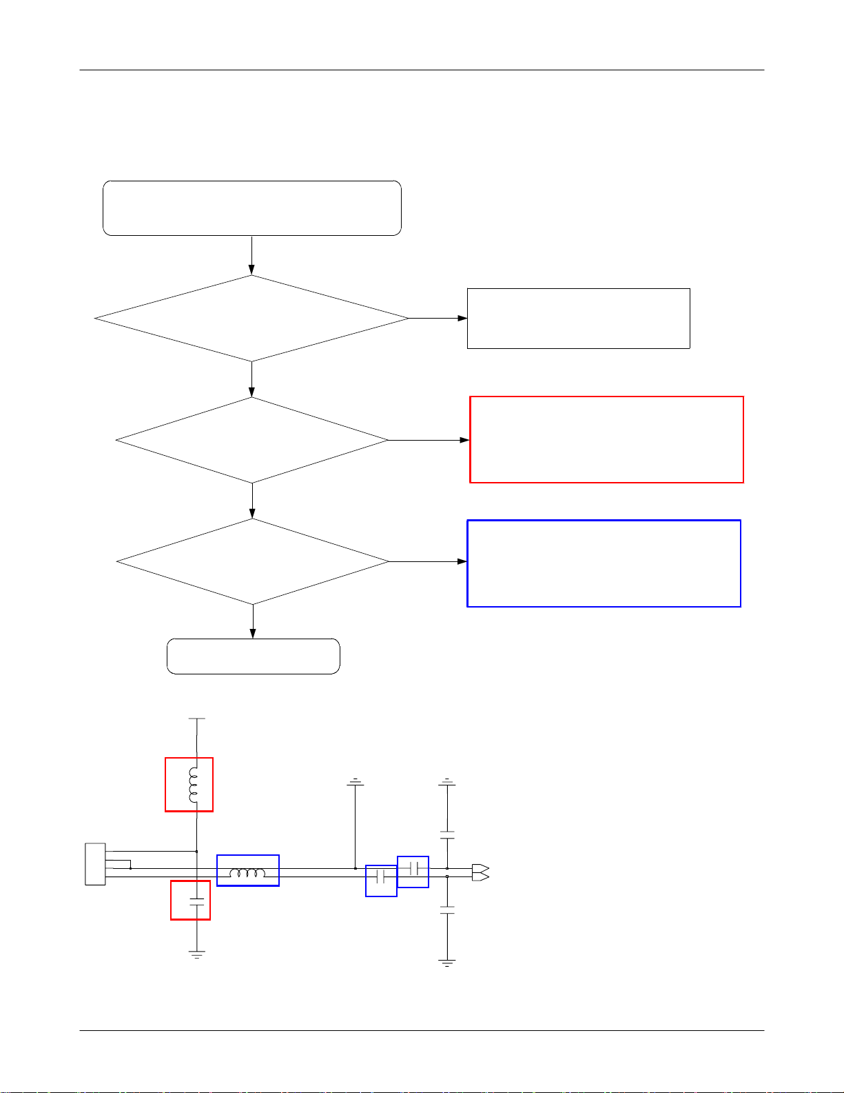
9-11
Bluetooth Part
Bluetooth does not work
C227
Is C243 ok?
Is BT_ANT ok?
Yes
>=2.75v ?
Yes
Yes
No
No
No
①
Check U402&Replace it
②
Check the C243
if it has problem, replace it)
(
③
Check the BT_ANT
if it has problem,replace it)
(
Yes
Check U201
Yes
END
No
④
Check U201
if it has problem,replace it)
(
9-22
SAMSUNG Proprietary-Contents may change without notice
This Document can not be used without Samsung's authorization
Page 23

CLK26M_BT
RTCCLK
BT_CLKREQ
Flow Chart of Troubleshooting
VBT_2V75
VBT_2V75 VDDE_1V8
C226
VDDE_1V8
C235
VDDE_1V8
C227
C228
C229
C230
C232
7
7
E
D
L
C
_
D
D
V
E6
GPIO_0
B5
GPIO_8
C2
GPIO_9
C1
GPIO_10
B3
GPIO_11
B4
GPIO_16
E2
CONFIG_1
F1
CONFIG_2
F2
CONFIG_3
F7
CLK_REQ_IN_1
G7
CLK_REQ_IN_2
C5
CLK_REQ_OUT_1
G3
CLK_REQ_OUT_2
D6
REF_CLK_IN
F3
LP_CLK
2
B
C233
C234
7
4
6
1
2
7
1
7
B
C
B
A
G
G
G
G
F
A
B
A
D
D
N
D
M
_
_
_
_
L
_
R
_
S
V
_
V
C
D
D
D
IO
IO
_
H
D
H
_
D
D
_
_
_
_
D
D
V
V
D
D
D
D
D
D
V
D
D
D
D2
D
D
V
V
V
V
V
V
PCM_A
PCM_B
PCM_CLK
PCM_SYNC
TOUT_IN_QP
TOUT_IP_QN
UART_RXD
UART_TXD
U201
UART_CTS
UART_RTS
RFN
RFP
AF_PRG
RESETN
BT_WAKEUP
1
3
2
_
_
_
1
HOST_WAKEUP
A
A
A
_
F
IG
IG
N
N
N
A
R
A
D
D
A
_
_
_
_
_
_
S
S
S
S
S
S
C
C
S
S
S
S
S
S
V
V
V
V
V
V
N
N
5
6
4
6
1
1
2
E
B
A
D
C
ACC_PCM_DLD_ST
E1
ACC_PCM_ULD_ST
D1
ACC_PCM_CLK
C3
ACC_PCM_SYNC
A6
A4
G5
F5
E3
E5
A2
A3
F4
D3
C4
F6
BT_RST
BT_ACC_SPI_IRQ
ACC_SPI_MOSI
ACC_SPI_MISO
ACC_SPI_CLK
BT_ACC_SPI_CSn
1
0
3
2
1
2
T
2
3
1
N
F207
1
BAL
3
BAL
C
C
N
N
6
C243
7
UNBAL
G
G
G
2
4
8
5
A
7
C242C241
4
2
C
9-23
SAMSUNG Proprietary-Contents may change without notice
This Document can not be used without Samsung's authorization
Page 24

Flow Chart of Troubleshooting
9-12-1.
EGSM
850
RX
NORMAL CONDITION
catch the channel?
YES
PAM101 CHECK
pin
#17≥-55
U101 CHECK
pin
#16≥-55
dBm?
YES
dBm?
YES
NO
NO
NO
CHECK
ANT contact
RFS
re-solder or change
C100,L100
100,
re-solder or change
U101
Band:GSM850
CELL POWER
Channel
:-50
: 160
dBm
Ch
F100 CHECK
pin#9
Rx Path CHECK
U102 pin#44
OSC CLOCK CHECK
U102 pin#17,18
freq:26MHz?
U102 CHECK
UCP303 CHECK!!
dBm?
-55
≥
YES
-55
≥
YES
YES
YES
dBm?
?
NO
NO
NO
NO
F100
re-solder or change
C105, L101
re-solder or change
OSC101
re-solder or change
U102
change or re-solder
9-24
SAMSUNG Proprietary-Contents may change without notice
This Document can not be used without Samsung's authorization
Page 25

Flow Chart of Troubleshooting
9-12-2.
EGSM
900
RX
NORMAL CONDITION
catch the channel?
YES
U101 CHECK
pin
#17≥-55
U101 CHECK
pin
#15≥-55
dBm?
YES
dBm?
YES
NO
NO
NO
CHECK
ANT contact
RFS
re-solder or change
C100,L100
100,
re-solder or change
U101
Band:GSM900
CELL POWER
Channel
:-50
:62
dBm
Ch
F100 CHECK
pin#6
Rx Path CHECK
U102 pin#46
OSC CLOCK CHECK
U102 pin#17,18
freq:26MHz?
U102 CHECK
UCP303 CHECK!!
dBm?
-55
≥
YES
-55
≥
YES
YES
YES
dBm?
?
NO
NO
NO
NO
F100
re-solder or change
C109, L102
re-solder or change
OSC101
re-solder or change
U102
change or re-solder
9-25
SAMSUNG Proprietary-Contents may change without notice
This Document can not be used without Samsung's authorization
Page 26

Flow Chart of Troubleshooting
9-12-3.
DCS1800 RX
NORMAL CONDITION
catch the channel?
YES
U101 CHECK
pin
#17≥-55
U101 CHECK
pin
#14≥-55
dBm?
YES
dBm?
YES
NO
NO
NO
CHECK
ANT contact
RFS
re-solder or change
C100,L100
100,
re-solder or change
U101
Band:DCS1800
CELL POWER
Channel
:-50
: 690
dBm
Ch
F101 CHECK
pin#9
Rx Path CHECK
U102 pin#48
OSC CLOCK CHECK
U102 pin#17,18
freq:26MHz?
U102 CHECK
UCP303 CHECK!!
dBm?
-55
≥
YES
-55
≥
YES
YES
YES
dBm?
?
NO
NO
NO
NO
F101
re-solder or change
C114, L104
re-solder or change
OSC101
re-solder or change
U102
change or re-solder
9-26
SAMSUNG Proprietary-Contents may change without notice
This Document can not be used without Samsung's authorization
Page 27

Flow Chart of Troubleshooting
9-12-4.
PCS1900 RX
NORMAL CONDITION
catch the channel?
YES
U101 CHECK
pin
#17≥-55
U101 CHECK
pin
#13≥-55
dBm?
YES
dBm?
YES
NO
NO
NO
CHECK
ANT contact
RFS
re-solder or change
C100,L100
100,
re-solder or change
U101
Band:PCS1900
CELL POWER
Channel
:-50
: 660
dBm
Ch
F101 CHECK
pin#6
Rx Path CHECK
U102 pin#50
OSC CLOCK CHECK
U102 pin#17,18
freq:26MHz?
U102 CHECK
UCP303 CHECK!!
dBm?
-55
≥
YES
-55
≥
YES
YES
YES
dBm?
?
NO
NO
NO
NO
F101
re-solder or change
C116, L105
re-solder or change
OSC101
re-solder or change
U102
change or re-solder
9-27
SAMSUNG Proprietary-Contents may change without notice
This Document can not be used without Samsung's authorization
Page 28

Flow Chart of Troubleshooting
9-12-5.
WCDMA2100 RX
NORMAL CONDITION
catch the channel?
YES
U101 CHECK
pin
#17≥-55
U101 CHECK
pin
#18≥-55
dBm?
YES
dBm?
YES
NO
NO
NO
CHECK
ANT contact
RFS
re-solder or change
C100,L100
100,
re-solder or change
U101
Band:WCDMA2100
CELL POWER
Channel
:-50
: 10700
dBm
Ch
F204 CHECK
pin#5
Rx Path CHECK
U102 pin#42
OSC CLOCK CHECK
U102 pin#17,18
freq:26MHz?
U102 CHECK
UCP303 CHECK!!
dBm?
-55
≥
YES
-55
≥
YES
YES
YES
dBm?
?
NO
NO
NO
NO
F204,C219,L214
re-solder or change
C224, L213
re-solder or change
OSC101
re-solder or change
U102
change or re-solder
9-28
SAMSUNG Proprietary-Contents may change without notice
This Document can not be used without Samsung's authorization
Page 29

Flow Chart of Troubleshooting
9-12-6.
EGSM
850/900
TX
TX Power is too Low!!
OSC CLOCK CHECK
U102 pin#17,18
freq:26MHz?
YES
U102 CHECK
Pin#54
U101 CHECK
Pin#3
dBm?
3
≥
YES
dBm?
0
≥
YES
NO
NO
NO
OSC101
re-solder or change
U102,
change or re-solder
R103, R104, R105
change or re-solder
Band:GSM850/900
CELL POWER
Tx Power:5Level
Channel
: 160/62
:-50
dBm
ch
TX Mode CHECK
U101 Pin#6
U101 CHECK
Pin#17
Pin#1
re-solder or change
30
≥
RFS100
30
≥
Antenna
≥
YES
dBm?
YES
dBm?
YES
1.2V?
NO
NO
NO
UCP303
re-solder or change
U101
change or re-solder
C100, L100
change or re-solder
9-29
SAMSUNG Proprietary-Contents may change without notice
This Document can not be used without Samsung's authorization
Page 30

Flow Chart of Troubleshooting
9-12-7.
DCS1800/PCS1900 TX
TX Power is too Low!!
OSC CLOCK CHECK
U102 pin#17,18
freq:26MHz?
U102 CHECK
Pin#56
≥
U101 CHECK
Pin#1
≥
YES
dBm?
3
dBm?
0
YES
YES
NO
NO
NO
OSC101
re-solder or change
U102,
change or re-solder
R106, R107, R108,C119
change or re-solder
Band:DCS1800/PCS1900
CELL POWER
Tx Power:0Level
Channel
:-50
: 690/660
dBm
ch
TX Mode CHECK
U101 Pin#6,7
U101 CHECK
Pin#17
Pin#1
re-solder or change
27
≥
RFS100
27
≥
Antenna
≥
YES
dBm?
YES
dBm?
YES
1.2V?
NO
NO
NO
UCP303
re-solder or change
U101
change or re-solder
C100, L100
change or re-solder
9-30
SAMSUNG Proprietary-Contents may change without notice
This Document can not be used without Samsung's authorization
Page 31

Flow Chart of Troubleshooting
9-12-8.
WCDMA2100 TX
TX Power is too Low!!
OSC CLOCK CHECK
U102 pin#17,18
freq:26MHz?
YES
PAM302 CHECK
Pin#3
Pin#18
dBm?
0
≥
YES
U101 CHECK
dBm?
20
≥
YES
NO
NO
NO
OSC101
re-solder or change
U102,F205
change or re-solder
PAM302,F206,F204,C219,L214
change or re-solder
Band:WCDMA2100
CELL POWER
Tx Power
Channel
:24
: 9750
:-50
dBm
ch
dBm
TX Mode CHECK
U101 Pin#7
U101 CHECK
Pin#17
Pin#1
re-solder or change
20
≥
RFS100
20
≥
Antenna
≥
YES
dBm?
YES
dBm?
YES
1.2V?
NO
NO
NO
UCP303
re-solder or change
U101
change or re-solder
C100, L100
change or re-solder
9-31
SAMSUNG Proprietary-Contents may change without notice
This Document can not be used without Samsung's authorization
Page 32

Flow Chart of Troubleshooting
9-32
SAMSUNG Proprietary-Contents may change without notice
This Document can not be used without Samsung's authorization
Page 33

Flow Chart of Troubleshooting
VRAD_2V8
F100
1
9
IN
OUT
4
6
IN
OUT
G
G
G
G
G
G
0
2
3
5
7
8
1
F101
1
9
IN
OUT
4
6
IN
OUT
G
G
G
G
G
G
0
2
3
5
7
8
1
WTX_HB3
VDDE_1V8
C124
C126
ANTSW2
ANTSW1
ANTSW0
ANTSW3
RFS100
G
A
C
G
4
2
1
3
VBAT
C100
C103
L100
7
1
3
6
7
8
9
C111
10
C112
1
HB_RF_IN
LB_RF_IN
BS2
BS1
_TXEN
MODE
RSVD
D
D
D
D
D
D
D
D
N
N
N
N
N
N
N
N
G
G
G
G
G
G
G
G
2
5
1
4
3
2
1
6
2
1
2
1
2
2
2
2
2
GTX_VAM
GTX_850_900
GTX_1800_1900
EDATA_AMP_FREQ_LSB
EDATA_QDATA_AMP_MSB
EDATA_IDATA_FREQ_MSB
4
T
N
A
U101
D
D
D
N
N
N
G
G
G
7
9
8
2
2
2
EDATA_STR
RF_CTRL_STR1
RF_CTRL_DATA
RF_CTRL_CLK
CLK26M_DB
CLK26M_BT
5
C
P
A
V
D
N
G
0
3
WRX_Q_N
WRX_Q_P
WRX_I_N
WRX_I_P
TESTOUT
MCLKREQ
C102
C106
GTX_VAM
T
T
A
B
V
D
N
G
1
3
16
RX1
RX2
RX3
RX4
WCDMA1
WCDMA2
WCDMA3
D
D
D
D
N
N
N
N
G
G
G
G
3
2
4
3
3
3
GRX_850
15
GRX_900
14
GRX_1800
13
GRX_1900
18
WRF_BAND_I
19
WRF_BAND_VIII
20
R103
R104
R105
R106
801R911C
R107
9
8
7
5
5
5
D
C
C
N
N
N
G
1
WRXQN
2
WRXQP
3
WRXIN
4
WRXIP
5
GND
6
EDATAC
7
EDATASTR
8
EDATAA
9
EDATAB
10
STR
11
DATA
12
CLK
13
TESTOUT
14
CLKREQ
K
L
C
M
5
1
R111
OSC101
43
1
ANT101
U720
1
1
1
1
2
2
2
2
3
3
3
3
C107
L103
GTX_1800_1900
GTX_850_900
GRX_850
GRX_900
GRX_1800
GRX_1900
VRAD_2V8
C117
0
1
3
4
2
5
6
7
8
9
5
5
5
5
5
5
5
4
4
4
2
2
1
D
D
D
D
B
B
D
B
A
B
L
N
N
N
N
H
O
H
C
X
H
X
G
G
G
G
M
T
X
X
C
T
M
E
R
R
V
E
A
E
E
E
U102
C
E
P
N
S
Q
IN
IP
Q
K
D
L
X
X
X
D
N
G
7
6
1
1
X
D
D
N
P
C
T
T
T
T
C
N
N
O
C
O
X
W
V
M
X
G
G
W
W
W
1
0
8
5
9
2
4
3
6
2
2
1
2
1
2
2
2
2
P
P
N
N
_
_
_
I
I_
Q
Q
_
_
_
_
X
X
X
X
T
2
T
T
T
W
W
W
W
C104
C108
C113
C115
C118
ERxHB2
ERxHB1
ERxLB2
ERxLB1
3
4
5
6
4
4
4
4
1
2
D
D
B
B
N
N
L
L
G
G
X
X
R
R
E
E
42
WRXHB2
GND
WRXLB
GND
WRXHB1
RFCTRL1
RFCTRL2
WTXLB
GND
WTXHB2
GND
WTXHB3
GND
WTXHB1
1
A
D
C
N
C
V
G
7
8
2
2
WRX_HB2
41
40
WRX_LB
39
38
37
36
35
WTX_LB
34
33
C130
32
31
C131
30
29
C105
L101
C109
L102
ERxLB1
ERxLB2
C114
ERxHB1
L104
C116
ERxHB2
L105
WTX_HB3
F205
1IN4
OUT
G2G3G
5
PWR_DET_B8
F202
3
COUPLING
VBAT
C212
C211
C213
PAM302
110
VCC1
VCC2
9
C217
BIAS_CTRL_2
BIAS_CTRL
WPA_A_EN
C223
2
3
4
5
RFIN
VMODE
VEN
GND
8
RFOUTVBP
D
N
G
1
1
L211
7
GND
L212
6
GND
2
IN1OUT
C225
3
COUPLING
TERMINATE
4
R207
PWR_DET_B1
F206
WRX_HB2
IN1OUT
TERMINATE
4
R201
F204
7
X
T
1
G
3
G
4
T
G
2
6
N
G
A
8
G
9
G
X
R
5
C219
C222
L214C221
WRF_BAND_I
C224
L213
C244
9-33
SAMSUNG Proprietary-Contents may change without notice
This Document can not be used without Samsung's authorization
Page 34

Block Diagrams
7.
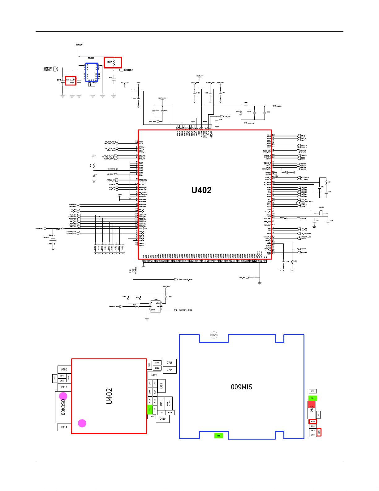
7-1.
Block Diagram
7-1
SAMSUNG Proprietary-Contents may change without notice
This Document can not be used without Samsung's authorization
Page 35

PCB Diagrams
8.
0
3
5
R
C507
0
4
5
R
R
R
6
6
1
1
2
1
0
4
7
C
F
6
0
4
F
6
0
2
J
C
O
N
3
0
0
C
5
0
3
U
5
1
R
0
0
3
5
C
0
9
5
U
3
0
0
L301
1
0
2
2
3
3
C
C
R115
R114
R113
R112
K
E
Y
P
A
D
K
E
Y
P
D
A
P
Y
E
1
K
E
Y
P
A
D
K
E
Y
P
A
D
L
E
D
2
4
6
0
6
K
E
Y
P
A
D
K
E
Y
P
A
D
D
A
P
Y
E
K
D
A
P
Y
E
K
7
D
A
P
Y
E
K
D
A
P
Y
E
K
R
A
T
S
R
R
6
0
8
L
E
D
4
K
D
A
P
Y
E
K
2
1
D
E
D
A
P
Y
E
K
D
A
P
Y
E
K
L
5
0
6
R
5
D
A
P
Y
E
K
D
A
P
Y
E
K
8
R
6
0
7
L
E
D
3
0
KEYPAD
A
D
3
K
E
Y
P
A
D
K
E
Y
P
A
D
6
K
E
Y
P
A
D
K
E
Y
P
A
D
9
P
R
A
H
S
D
A
P
Y
E
K
D
A
P
Y
E
K
KEYPAD
8-1
SAMSUNG Proprietary-Contents may change without notice
This Document can not be used without Samsung's authorization
Page 36

PCB Diagrams
L
6
0
0
H
Y
0
7
A
B
0
7
2
0
C
6
2
1
H
D
C
6
0
2
R604
C
2
4
7
A
N
T
2
0
1
H
Y
0
7
A
B
0
7
2
0
BOTHHOLE301
BOTHHOLE
BOTHHOLE
S
C
3
0
7
M
_
A
C
5
0
3
C
S
BOTHHOLE303
BOTHHOLE
BOTHHOLE
R
6
0
3
C
6
1
1
U602
R406
R
4
0
5
U
4
R407
0
3
R
5
1
5
0
0
5
U
R
5
1
1
R513
C304
C
A
T
R
C305
5
2
2
C
6
0
1
C313
C312
ZD602
Q300
ZD603
C215
C214
M
I
C
7
4
C
0
5
6
C
1
T
1
2
2
5
A
C
5
0
3
R
6
1
0
1
0
C
6
C
C
2
2
4
4
1
2
3
4
2
C
0
6
C
3
S
D502
4
3
2
C
C227
E-STLC2584TR
1
0
5
L
E-STLC2584TR
C
5
0
6
I
F
ZD502
C
5
ZD503
0
0
5
0
5
C
C
4
0
5
6
1
4
C
R
4
0
1
R
4
4
0
0
4
3
C
C402
C413
O
S
C
4
0
0
R408
C414
1
0
4
9
D
0
4
C
C
3
0
1
R
5
1
8
C
C
3
3
0
0
3
9
C
3
0
2
R315
0
7
U201
C230
2
C
4
2
5
D
4
0
0
UCP303
2
F
C
2
2
6
Z
D
5
0
1
C236
0
5
L
C422
C421
2
0
4
U
L400
C408
C
3
1
0
BTC500
KQ03SB1-3R
KQ03SB1-3R
C
C
2
2
9
5
0
1
C233
C
2
3
2
C
2
3
5
2
0
5
C
C
2
2
8
C
C
2
2
0
5
3
3
4
4
1
7
2
2
C
C
U206
SI4709-B-GMR
SI4709-B-GMR
0
2
4
C
2
3
8
C
6
2
4
4
C
4
1
2
1
1
2
4
3
C
4
2
4
U
4
0
1
0
0
1
3
B
A
C401
0
6
4
C
0
2
5
R
R
3
0
2
C
5
1
0
R301
5
R
2
0
5
2
1
9
5
5
C
U
2
0
R
5
2
0
3
5
0
R
5
2
1
5
L
U
R516
C
7
2
7
4
5
0
0
5
5
1
7
C
0
L
L
9
3
2
L
C
2
0
7
C
7
1
C
2
C
7
1
4
C
C
C
4
0
0
C
7
1
7
C
1
7
0
5
0
7
U
1
2
7
C
C713
C718
2
2
7
C
C715
C714
9
1
4
C
7
3
7
C
3
9
3
3
7
7
C
C
3
0
7
L
0
C
R
7
7
8
3
7
0
C
1
3
4
2
7
C
B
C
A
7
0
7
C
4
0
3
9
8
1
1
3
3
R
R
R309
R
3
0
7
C
3
0
6
3
2
3
C
C
3
0
8
4
2
3
C
2
1
2
R
ZD703
3
0
6
1
U
7
1
8
3
0
L
7
7
1
C
0
0
6
3
7
C
1
7
C
5
2
7
C
R701R703
C410
VDCIO_FOG
DB3200DT
DB3200DT
R
Z
4
0
6
D
C300
R322
0
0
4
R
O
S
C
1
0
1
R
F
C
R
3
2
2
1
0
R111
6
3
3
0
6
2
0
1
C
X
X
D
D
2
S
S
1
1
0
2
2
2
2
2
V
V
4
2
1
M
M
U
C
L
L
R
C
2
6
5
2
0
0
0
2
2
2
2
3
R
R
F
5
2
0
C
2
7
2
1
5
R204
2
C
A
A
P
C
C
P
P
A
M
M
-
-
M
7
7
3
3
8
8
3
3
3
0
-
S
S
2
G
G
1
1
2
0
7
L
3
4
7
C
0
1
2
2
L211L212
0
R
R
R
3
3
7
4
1
R300
5
R
0
0
4
H
T
R
F
3
3
0
0
C
F
1
3
1
2
0
3
C
1
3
0
1
C
C
1
2
2
0
1
2
1
3
C
C
C
2
2
0
1
2
2
R
2
0
7
C
F206
2
2
0
0
0
0
1
4
3
3
9
0
C
9
1
1
C
R
1
0
6
R108
R
1
0
7
R
1
4
0
0
3
1
R
R
1
0
5
C
C
1
1
1
1
U
7
8
1
0
6
1
1
C
L
1
0
2
4
0
2
L
A
C
P
M
7
3
7
3
S
G
1
5
C
1
1
4
L104
1
0
L
1
0
2
1
F
C
1
0
9
5
1
1
C
L101
C
1
0
5
3
1
1
0
C
0
4
4
C
L
L
2
2
0
3
C
2
0
5
1
2
2
C
1
2
4
A
C
P
M
7
3
7
3
S
G
1
8
F
3
0
1
C
4
0
1
C
C
2
1
0
C209
R
2
0
1
P
2
2
0
F
A
M
C207
3
0
1
L208
9
0
2
L
C331
2
1
1
C
1
1
1
C
S
S
K
K
Y
Y
7
7
7
7
5
5
2
2
1
1
L
C208
2
1
4
4
9
1
2
C
0
2
F201
2
2
2
F
C
SC301SC302
4
0
5
D
Z
S
C
H
B
1
A
0
1
0
3
ZD605 ZD606
U
1
0
1
L
2
1
0
C734
C614
1
0
6
HEA1
U
C
5
2
0
5
3
S
S
C
2
4
6
L103
A
N
T
1
0
1
C
R
R
R
R615
7
9
8
6
6
6
4
0
0
1
1
1
2
6
6
4
3
6
C
C
C
6
2
0
C
6
1
5
C741
S
C
H
B
1
A
0
1
0
3
SC304
C
7
C
3
0
6
0
1
3
R
-
1
.
9
0
P
-
0
5
6
0
P
-
-
6
1
.
9
0
0
5
0
0
0
6
I
M
S
2
1
5
R
C
1
0
6
C
5
0
8
R
5
2
1
1
5
0
C
C
1
0
2
C511
USB3310C-CP-TR
5
1
5
C
0
0
1
L
0
0
1
C
RFS100
C107
KMS-560
KMS-560
USB3310C-CP-TR
C
3
2
7
C
3
3
0
3
0
1
C
U
7
2
0
C622 C623
U501
C
3
2
9
N
1
K
V
C
D
6
0
1
BOTHHOLE302
C604C605C606
BOTHHOLE
BOTHHOLE
H
D
C
6
0
1
C
3
2
5
R505
0
0
6
D
C
3
2
8
C
6
1
9
C
6
1
8
R
C616
6
1
7
C
6
1
7
C
C
2
0
4
R
3
3
2
2
N
B
L
4
1
BOTHHOLE304BOTHHOLE305
2
6
B
A
T
B
4
L
4
0
1
0
4
L
/
F
4
9
L
M
/
F
E
9
M
E
8-2
SAMSUNG Proprietary-Contents may change without notice
This Document can not be used without Samsung's authorization
 Loading...