

Samsung S5250 Service Manual
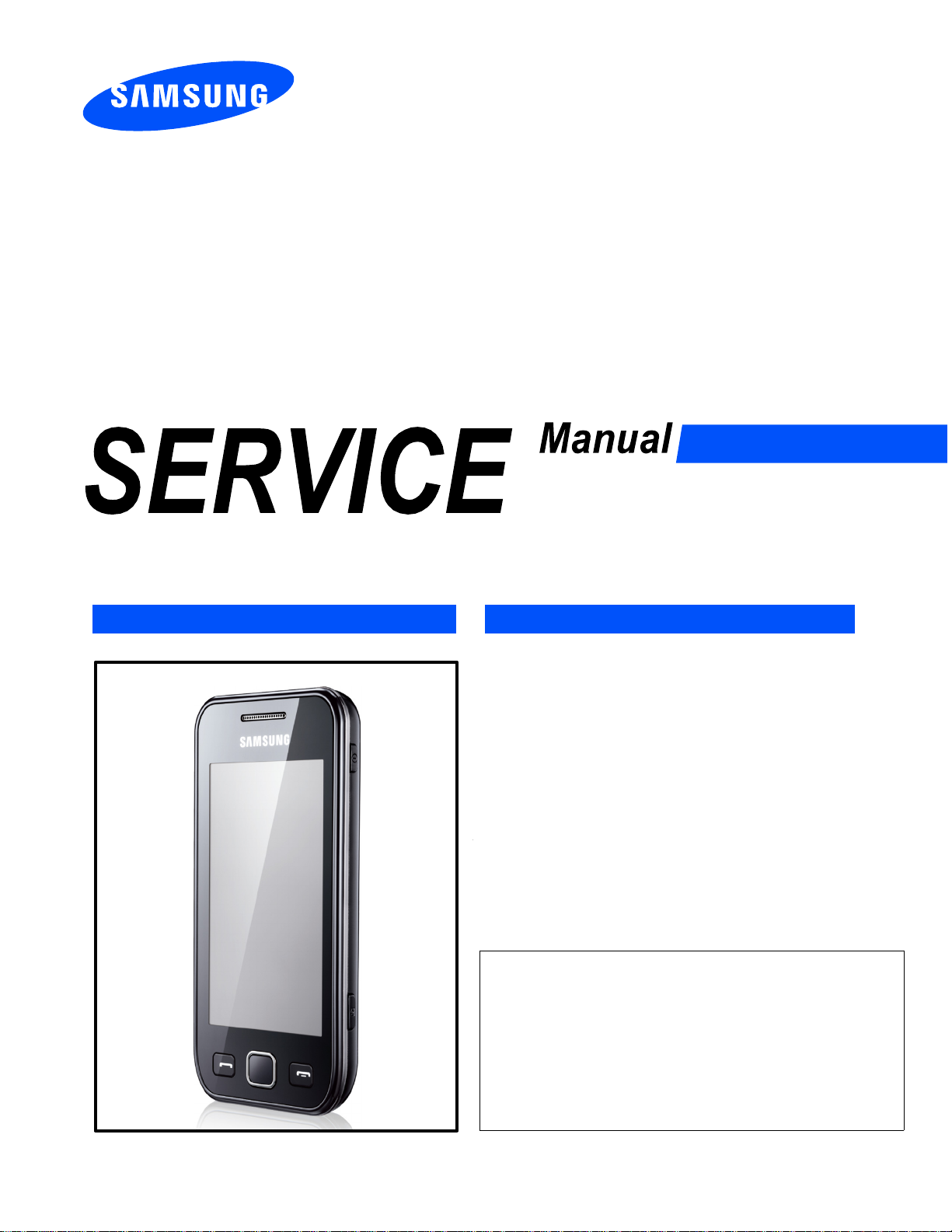
GSM TELEPHONE
GT-S5250
GSM TELEPHONE
CONTENTS
Safety Precautions
1.
Specification
2.
Product Function
3.
Exploded View and Parts list
4.
MAIN Electrical Parts List
5.
Level1Repair
6.
Disassembly and Assembly
7.
Instructions
Chart of Troubleshooting
8.
Reference data
9.
Notice
All functionality, features, specifications and other
product information provided in this document inclu
ding, but not limited to, the benefits, design, pricing,
components, performance, availability, and capabiliti
es of the product are subject to change without
-
notice or obligation. Samsung reserves the right to
make changes to this document and the product
described herein, at anytime, without obligation on
Samsung to provide notification of such change.
:

Safety Precautions
1.
Repair Precaution
1-1.
Repair in Shield Box, during detailed tuning. Take specially care of tuning or test, because
―
specipicty of cellular phone is sensitive for surrounding interference(RF noise).
Be careful to useakind of magnetic object or tool, because performance of parts is damaged by
―
the influence of magnetic force.
Surely useastandard screwdriver when you disassemble this product, otherwise screw will be
―
worn away.
Useathicken twisted wire when you measure level.
―
thicken twisted wire has low resistance, therefore error of measurement is few.
A
Repair after separate Test Pack and Set because for short danger(for example an overcurrent
―
and furious flames of parts etc) when you repair board in condition of connecting Test Pack and
tuning on.
Take specially care of soldering, because Land of PCB is small and weak in heat.
―
Surely tune on/off while using AC power plug, becausearepair of battery charger is dangerous
―
when tuning ON/OFF PBA and Connector after disassembling charger.
Don't use as you pleases after change other material than replacement registered on SEC System.
―
Otherwise engineer in charge isn't charged with problem that you don't keep this rules.
1-1
SAMSUNG Proprietary-Contents may change without notice
This Document can not be used without Samsung's authorization

Safety Precautions
ESD(Electrostatically Sensitive Devices) Precaution
1-2.
Several semiconductor may be damaged easily by static electricity. Such parts are called by ESD
Electrostatically Sensitive Devices), for example IC,BGA chip etc. Read Precaution below.
(
You can prevent from ESD damage by static electricity.
Remove static electricity remained your body before you touch semiconductor or parts with
―
semiconductor. There are ways that you touch an earthed place or wear static electricity prevention
string on wrist.
Use earthed soldering steel when you connect or disconnect ESD.
―
Use soldering removing tool to break static electricity.,otherwise ESD will be damaged by static
―
electricity.
Don't unpack until you set up ESD on product. Because most of ESD are packed by box and
―
aluminum plate to have conductive power,they are prevented from static electricity.
You must maintain electric contact between ESD and place due to be set up until ESD is
―
connected completely to the proper place oracircuit board.
1-2
SAMSUNG Proprietary-Contents may change without notice
This Document can not be used without Samsung's authorization
Specification
2.
GSM General Specification
2-1.
GSM900
Phase 1
Freq.
Band[MHz]
Uplink/Downlink
ARFCN range
Tx/Rx spacing 45MHz 45MHz 95MHz 80MHz
Mod. Bit rate/
Bit Period
Time Slot
Period/Frame
Period
Modulation 0.3GMSK 0.3GMSK 0.3GMSK 0.3GMSK
MS Power 33dBm~5dBm 33dBm~5dBm 30dBm~0dBm 30dBm~0dBm
880~915
925~960
0~124 &
975~1023
270.833kbps
3.692us
576.9us
4.615ms
GSM850
Phase 1
824.2~848.8
869.2~893.8
128~251 512~885 512~810
270.833kbps
3.692us
576.9us
4.615ms
DCS1800
Phase 1
1710~1785
1805~1880
270.833kbps
3.692us
576.9us
4.615ms
PCS1900
1850~1910
1930~1990
270.833kbps
3.692us
576.9us
4.615ms
Power Class 5pcl ~ 19pcl 5pcl ~ 19pcl 0
Sensitivity -102dBm -102dBm -100dBm -100dBm
TDMAMux8888
Cell Radius 35Km 35Km 2Km -
pcl
~15
pcl
pcl
0
~15
pcl
2-1
Speclflcation
GSM Tx Power Class
2-2.
TX Power
control level
533±3
631±3
729±3
827±3
925±3
10 23±3
11 21±3
GSM
GSM900
850
dBm
dBm
dBm
dBm
dBm
dBm
dBm
TX Power
DCS1800
control level
030±3
128±3
226±3
324±3
422±3
520±3
618±3
dBm
dBm
dBm
dBm
dBm
dBm
dBm
TX Power
control level
030±3
128±3
226±3
324±3
422±3
520±3
618±3
PCS1
900
dBm
dBm
dBm
dBm
dBm
dBm
dBm
12 19±3
13 17±3
14 15±3
15 13±3
16 11±5
17 9±5
18 7±5
19 5±5
dBm
dBm
dBm
dBm
dBm
dBm
dBm
dBm
716±3
814±3
912±4
10 10±4
11 8±4
12 6±4
13 4±4
14 2±5
15 0±5
dBm
dBm
dBm
dBm
dBm
dBm
dBm
dBm
dBm
716±3
814±3
912±4
10 10±4
11 8±4
12 6±4
13 4±4
14 2±5
15 0±5
dBm
dBm
dBm
dBm
dBm
dBm
dBm
dBm
dBm
2-2
GSM EDGE TX power class
2-3.
Speclflcation
Only in Master
TX Power
control level
827±3
925±3
10 23±3
11 21±3
12 19±3
13 17±3
14 15±3
GSM900
GSM850
dBm
dBm
dBm
dBm
dBm
dBm
dBm
TX Power
control level
2 26±3
3 24±3
4 22±3
5 20±3
6 18±3
7 16±3
8 12±3
DCS1800
dBm
dBm
dBm
dBm
dBm
dBm
dBm
TX Power
control level
226±3
324±3
422±3
520±3
618±3
716±3
812±3
PCS1900
dBm
dBm
dBm
dBm
dBm
dBm
dBm
15 13±3
16 11±5
17 9±5
18 7±5
19 5±5
dBm
dBm
dBm
dBm
dBm
9 10±3
10 14±3
11 12±4
12 10±4
13 8±4
14 6±4
15 4±4
2-3
dBm
dBm
dBm
dBm
dBm
dBm
dBm
910±3
10 14±3
11 12±4
12 10±4
13 8±4
14 6±4
15 4±4
dBm
dBm
dBm
dBm
dBm
dBm
dBm

Operation Instruction and Installation
3.
Main Function
Bada OS
GSM Quad Band/EDGE
WQVGA, TFT
3.2’’
FF Camera+Video Rec.
3M
Wi-Fi/BT v3.0+EDR/USB v2.0
A-GPS
FM Radio with RDS+Rec.
TouchWiz
MB internal memory/microSD(upto16G)
100
mAh standard Battery
1200
3.0
262K
UI/Dolfin Browser/Social Hub/DNSe
3-1
SAMSUNG Proprietary-Contents may change without notice
This Document can not be used without Samsung's authorization
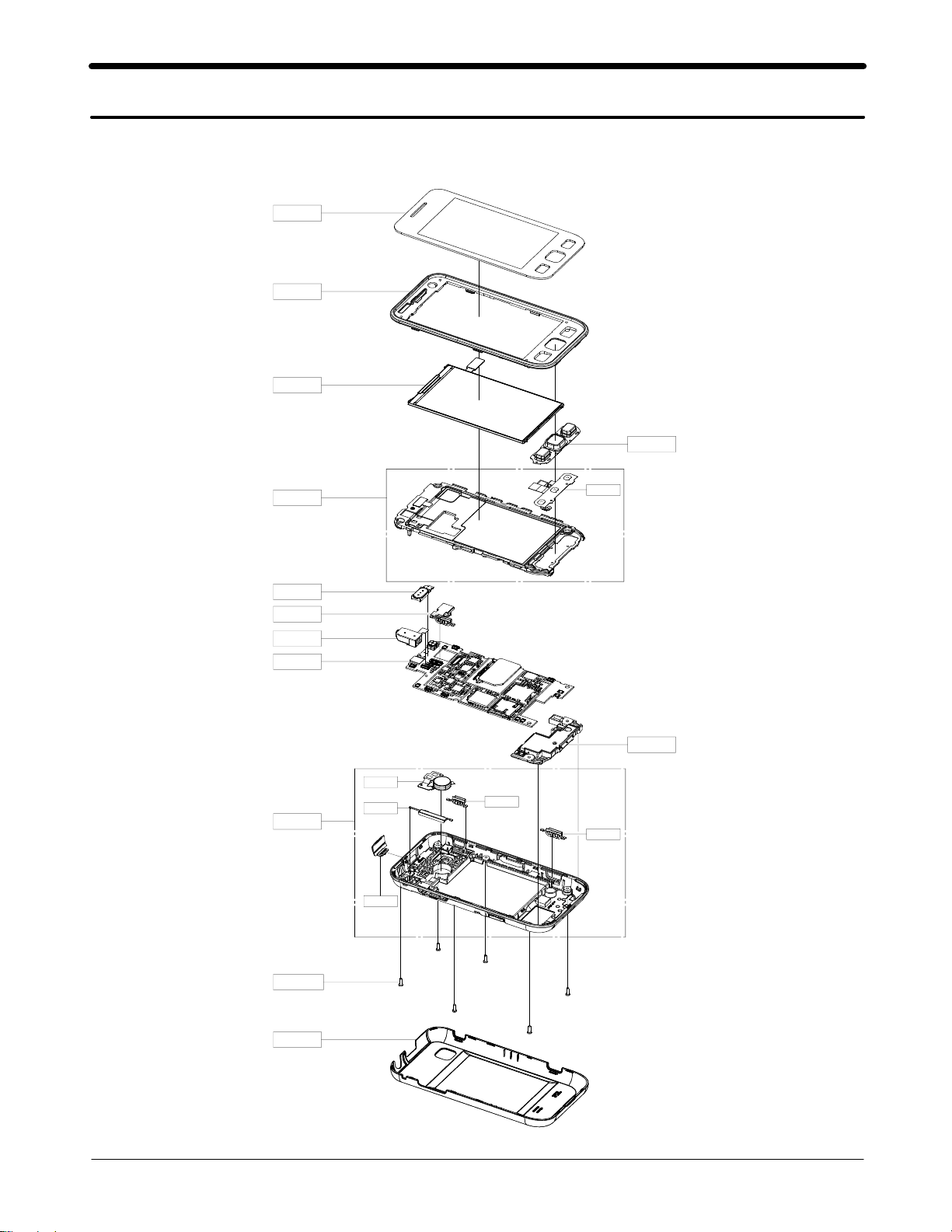
Exploded View and Parts List
4.
Cellular phone Exploded View
4-1.
QME03
QFR01
QLC01
QKP01
QLB01
QAR01
QCA01
QJK01
QMP01
QRE01
QMO01
QVO01
QRF06
QME01
QSP01
QCK02
QCK01
QCR101
QBC00
4-1
SAMSUNG Proprietary-Contents may change without notice
This Document can not be used without Samsung's authorization
Exploded View and Parts List
Cellular phone Parts list
4-2.
Design LOC Description SEC CODE
QAR01 AUDIO-RECEIVER
QCR101 SCREW-MACHINE
3009-001499
6001-002005
QSP01 MODULE-SPK+INTENNA,GTS5250 GH59-09589A
QJK01 KEY FPCB-EARJACK ASSY(GT_S5250) GH59-09640A
QME03 TOUCH/PANEL-GT_S5250 GH59-09672A
QMP01 A/S ASSY-PBA MAIN(COMM)GT_S5250 GH82-05205A
QLC01 ASSY LCD-3.2"WQVGA GT-S5250 ASSY GH96-04762A
QCA01 ASSY CAMERA-MODULE,3M(GT_S5250) GH96-04935A
QFR01 ASSY CASE-FRONT GH98-17542A
QBC00 ASSY COVER-BATT GH98-17544A
QKP01 ASSY KEYPAD-MAIN GH98-17546A
QLB01 ASSY BRACKET-LCD GH98-17541A
QME01 KEY FPCB-MAIN KEY PBA(GT_S5250) GH59-09658A
QRE01 ASSY CASE-REAR GH98-17543A
QMO01 MOTOR DC-GT-S5250 GH31-00503A
QRF06 PMO COVER-USB GH72-60559A
QCK01 ASSY KEY-CAM GH98-17855A
QVO01 ASSY KEY-VOL GH98-17856A
QCK02 ASSY KEY-POWER GH98-17857A
4-2
SAMSUNG Proprietary-Contents may change without notice
This Document can not be used without Samsung's authorization
MAIN Electrical Parts List
5.
Main
5-1.
SEC CODE DESIGN LOC DESCRIPTION
0403-001688
0404-001172
0404-001504
0406-001223
0406-001293
0406-001293
0406-001293
0406-001293
0407-001002
0801-002970
0801-003130
1001-001585
1001-001607
1001-001655
1001-001664
1108-000353
1201-002943
1203-006331
1203-006456
1203-006468
1205-003866
1205-003868
1205-004046
1209-001817
1404-001221
2007-000138
2007-000138
2007-000139
2007-000140
2007-000141
2007-000141
2007-000143
2007-000144
2007-000148
2007-000156
2007-000162
ZD602 DIODE-ZENER
D200,D500 DIODE-SCHOTTKY
ZD102,ZD103 DIODE-SCHOTTKY
ZD400 DIODE-TVS
ZD403,ZD404,ZD405 DIODE-TVS
ZD406,ZD501,ZD502 DIODE-TVS
ZD503,ZD504,ZD601 DIODE-TVS
ZD603 DIODE-TVS
D600 DIODE-ARRAY
U603 IC
U200 IC
U602 IC
U100 IC
U402 IC
U201,U202 IC
UME200 MEMORY
PAM100 IC
U500 IC
U604 IC
U300 IC
U101 IC
U102 IC
UCP200 IC
U400 IC
VR200 THERMISTOR
R228,R229,R412,R502 R-CHIP
R611 R-CHIP
R214 R-CHIP
R106,R107,R221,R402 R-CHIP
R206,R207,R224,R225 R-CHIP
R407,R408 R-CHIP
R201,R501,R600,R601 R-CHIP
R209,R210,R211,R213 R-CHIP
R305 R-CHIP
R608 R-CHIP
R103,R105,R108,R110 R-CHIP
5-1
SAMSUNG Proprietary-Contents may change without notice
This Document can not be used without Samsung's authorization

MAIN Electrical Parts List
SEC CODE DESIGN LOC DESCRIPTION
2007-000162
2007-000162
2007-000162
2007-000170
2007-000172
2007-001288
2007-001323
2007-003018
2007-007092
2007-007132
2007-007193
2007-007312
2007-007315
2007-007981
2007-008401
2007-008517
2203-000233
2203-000254
2203-000278
2203-000278
2203-000425
2203-000438
2203-000550
2203-000627
2203-000679
2203-000696
2203-000812
2203-000812
2203-000854
2203-000995
2203-000995
2203-001101
2203-001153
2203-001221
2203-001383
2203-002487
2203-002709
R111,R204,R215,R216 R-CHIP
R218,R230,R231,R232 R-CHIP
R607,R610 R-CHIP
R223,R306 R-CHIP
R504 R-CHIP
R302,R303 R-CHIP
R403 R-CHIP
R102,R104 R-CHIP
R401 R-CHIP
R112,R113 R-CHIP
R200 R-CHIP
R217 R-CHIP
R219 R-CHIP
R202,R203 R-CHIP
R205 R-CHIP
R208 R-CHIP
C144,C235 C-CERAMIC,CHIP
C145,C224,C233 C-CERAMIC,CHIP
C108,C113,C131,C137 C-CERAMIC,CHIP
C138,C139,C140 C-CERAMIC,CHIP
C221 C-CERAMIC,CHIP
C126,C148,C231,C420 C-CERAMIC,CHIP
C303,C305 C-CERAMIC,CHIP
C147 C-CERAMIC,CHIP
C400,C404 C-CERAMIC,CHIP
C105 C-CERAMIC,CHIP
C107,C111,C112,C401 C-CERAMIC,CHIP
C402,C505 C-CERAMIC,CHIP
C201 C-CERAMIC,CHIP
C207,C218,C230,C237 C-CERAMIC,CHIP
C616 C-CERAMIC,CHIP
C225,C418,C419 C-CERAMIC,CHIP
C103 C-CERAMIC,CHIP
C106 C-CERAMIC,CHIP
C100 C-CERAMIC,CHIP
C604 C-CERAMIC,CHIP
C152,C321,C417,C608 C-CERAMIC,CHIP
5-2
SAMSUNG Proprietary-Contents may change without notice
This Document can not be used without Samsung's authorization

MAIN Electrical Parts List
SEC CODE DESIGN LOC DESCRIPTION
2203-005234
2203-005450
2203-005482
2203-006048
2203-006048
2203-006048
2203-006048
2203-006048
2203-006141
2203-006257
2203-006260
2203-006260
2203-006399
2203-006399
2203-006399
2203-006399
2203-006399
2203-006399
2203-006562
2203-006562
2203-006562
2203-006626
2203-006681
2203-006824
2203-006841
2203-006841
2203-006872
2203-006872
2203-006872
2203-006872
2203-006890
2203-007270
2203-007271
2203-007271
2203-007279
2203-007317
2203-007393
C110 C-CERAMIC,CHIP
C142 C-CERAMIC,CHIP
C101 C-CERAMIC,CHIP
C117,C118,C120,C121 C-CERAMIC,CHIP
C125,C203,C210,C212 C-CERAMIC,CHIP
C213,C214,C215,C219 C-CERAMIC,CHIP
C220,C239,C240,C317 C-CERAMIC,CHIP
C319,C610,C612 C-CERAMIC,CHIP
C601 C-CERAMIC,CHIP
C310,C311 C-CERAMIC,CHIP
C128,C129,C154,C232 C-CERAMIC,CHIP
C615 C-CERAMIC,CHIP
C200,C202,C209,C211 C-CERAMIC,CHIP
C304,C318,C322,C325 C-CERAMIC,CHIP
C328,C329,C330,C331 C-CERAMIC,CHIP
C332,C333,C340,C344 C-CERAMIC,CHIP
C346,C503,C504,C507 C-CERAMIC,CHIP
C508,C509,C614 C-CERAMIC,CHIP
C302,C323,C334,C405 C-CERAMIC,CHIP
C406,C407,C408,C409 C-CERAMIC,CHIP
C411,C605 C-CERAMIC,CHIP
C603 C-CERAMIC,CHIP
C216,C217,C227,C228 C-CERAMIC,CHIP
C502 C-CERAMIC,CHIP
C204,C312,C313,C316 C-CERAMIC,CHIP
C602 C-CERAMIC,CHIP
C119,C122,C123,C124 C-CERAMIC,CHIP
C130,C132,C133,C134 C-CERAMIC,CHIP
C143,C146,C205,C206 C-CERAMIC,CHIP
C208,C222,C223,C226 C-CERAMIC,CHIP
C314,C315,C339 C-CERAMIC,CHIP
C102 C-CERAMIC,CHIP
C115,C326,C327,C335 C-CERAMIC,CHIP
C336,C337,C338 C-CERAMIC,CHIP
C114,C501,C617 C-CERAMIC,CHIP
C127 C-CERAMIC,CHIP
C116,C135,C136 C-CERAMIC,CHIP
5-3
SAMSUNG Proprietary-Contents may change without notice
This Document can not be used without Samsung's authorization
MAIN Electrical Parts List
SEC CODE DESIGN LOC DESCRIPTION
2203-007687
2404-001377
2404-001506
2404-001516
2404-001572
2703-001409
2703-002198
2703-002205
2703-002206
2703-002207
2703-002208
2703-002281
2703-002313
2703-002608
2703-002900
2703-002901
2703-002918
2703-003004
2703-003260
2703-003476
2703-003485
2703-003698
2703-003878
2801-004551
2801-004954
2809-001362
2901-001454
2901-001454
2904-001759
2904-001912
2904-001913
2909-001324
3003-001136
3301-001438
3301-001534
3301-001659
3301-001789
C500 C-CERAMIC,CHIP
C410 C-TA,CHIP
C301 C-TA,CHIP
C606,C611 C-TA,CHIP
C300 C-TA,CHIP
L121,L122 INDUCTOR-SMD
L100 INDUCTOR-SMD
L126 INDUCTOR-SMD
L103 INDUCTOR-SMD
L106,L109 INDUCTOR-SMD
L101,L105,L116 INDUCTOR-SMD
L110,L113,L114,L118 INDUCTOR-SMD
L408,L410 INDUCTOR-SMD
L127 INDUCTOR-SMD
L111,L112 INDUCTOR-SMD
L102,L104 INDUCTOR-SMD
L107,L108 INDUCTOR-SMD
L115,L117 INDUCTOR-SMD
L300,L301 INDUCTOR-SMD
L501,L502,L503 INDUCTOR-SMD
L500 INDUCTOR-SMD
L124 INDUCTOR-SMD
L401 INDUCTOR-SMD
OSC300 CRYSTAL-UNIT
OSC200 CRYSTAL-UNIT
OSC100 OSCILLATOR-VCTCXO
F500,F501,F502,F503 FILTER-EMI SMD
F504 FILTER-EMI SMD
F103 FILTER-SAW
F100 FILTER-SAW
F101 FILTER-SAW
F102 FILTER-DUPLEXER
MIC400 MIC-CONDENSOR
L125 CORE-FERRITE BEAD
L119,L120 CORE-FERRITE BEAD
L123,L200,L201 CORE-FERRITE BEAD
L600 CORE-FERRITE BEAD
5-4
SAMSUNG Proprietary-Contents may change without notice
This Document can not be used without Samsung's authorization

MAIN Electrical Parts List
SEC CODE DESIGN LOC DESCRIPTION
3301-001810
3301-001885
3301-002065
3301-002065
3301-002065
3301-002078
3404-001410
3404-001410
3705-001731
3708-002222
3708-002283
3709-001575
3709-001625
3711-006615
3711-006865
3711-007312
3722-003065
L506 CORE-FERRITE BEAD
L507 CORE-FERRITE BEAD
L402,L403,L404,L405 CORE-FERRITE BEAD
L406,L508,L509,L510 CORE-FERRITE BEAD
L511 CORE-FERRITE BEAD
L407,L409 CORE-FERRITE BEAD
TA603,TAC600,TAC601 SWITCH-TACT
TAC602 SWITCH-TACT
RFS100 CONNECTOR-COAXIAL
SLC500 CONNECTOR-FPC/FFC/PIC
HDC400 CONNECTOR-FPC/FFC/PIC
CD300 CONNECTOR-CARD EDGE
SIM300 CONNECTOR-CARD EDGE
HDC500 CONNECTOR-HEADER
HDC501 CONNECTOR-HEADER
BTC600 CONNECTOR-HEADER
IFC600 JACK-PHONE
GH71-08731A ANT100,ANT101,ANT102 NPR-CONTACT ANT
GH71-08731A ANT103,MOT600,MOT601 NPR-CONTACT ANT
GH71-08731A SPK400,SPK401 NPR-CONTACT ANT
GH80-03320A R100,R101 PB-SHORT-1005
GH80-03321A R226 PB-SHORT-0603
RES-Z1005-S R404,R405 RES-Z1005-SHORT-P
RES-Z1005-S R404,R405 RES-Z1005-SHORT-P
Please consult the GSPN website(Samsung Portal) for the most recent version of the product's
part list.
5-5
SAMSUNG Proprietary-Contents may change without notice
This Document can not be used without Samsung's authorization
Level
6.
Software Download
6-1.
Repair
1
6-1-1.
-
Pre-requisite for Download
Downloader Program
GT-B7350 Mobile Phone
Data Cable
JIG BOX(GH99-36900A)
RF Test Cable(GH39-00985A)
JIG Cable(GH39-01338A)
Adapter(GH99-38251A)
Binary files
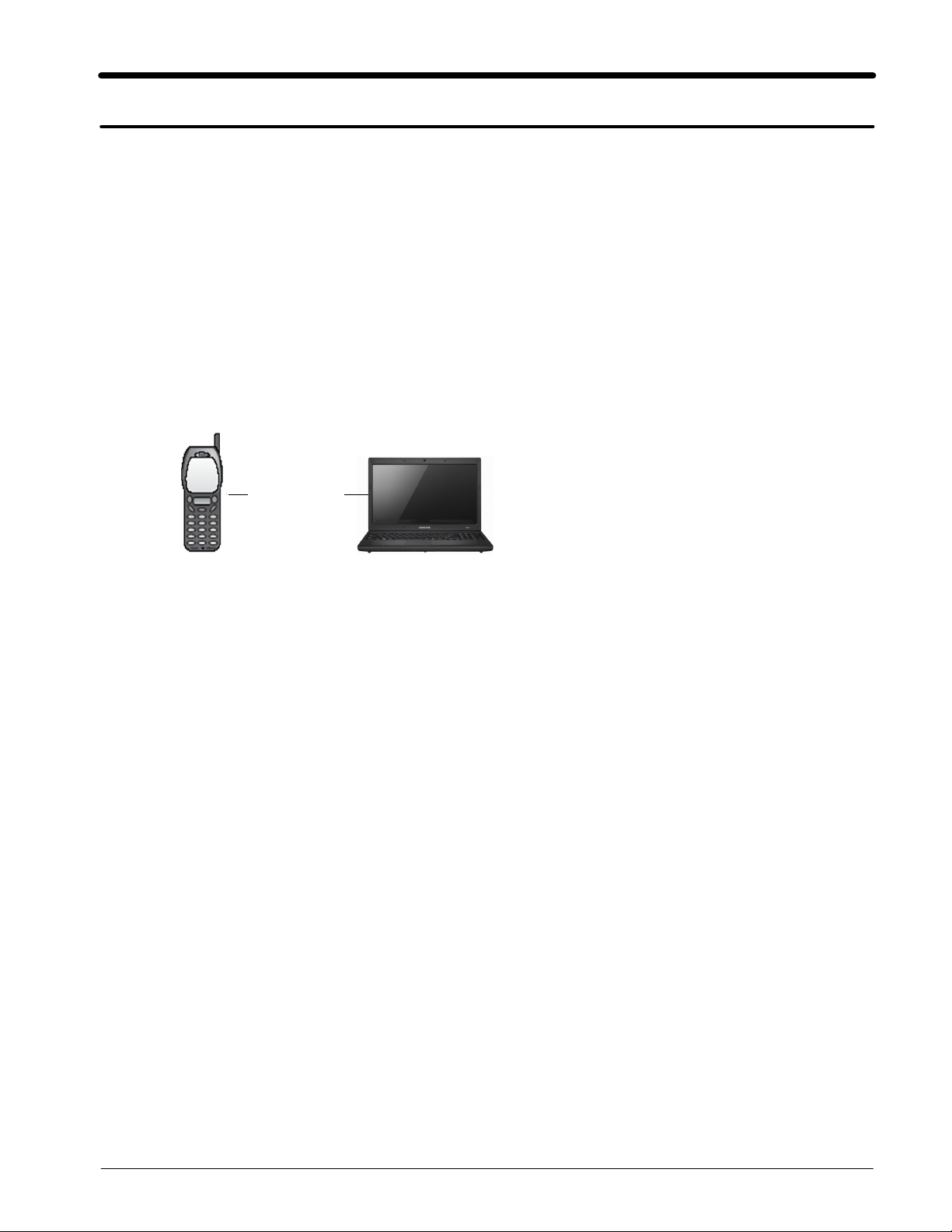
Diagram of Connection:
Mobile Phone(with Battery)
(
MSM7x27&MSM7X25_MultiDownloader.exe
Data Cable
)
PC
6-1
SAMSUNG Proprietary-Contents may change without notice
This Document can not be used without Samsung's authorization
Level1Repair
6-1-2.
}
S/W Download Process
Load the binary download program by executing the
1.
Load the binary download program by executing the
1.
"Downloader V5.64"
6-2
SAMSUNG Proprietary-Contents may change without notice
This Document can not be used without Samsung's authorization
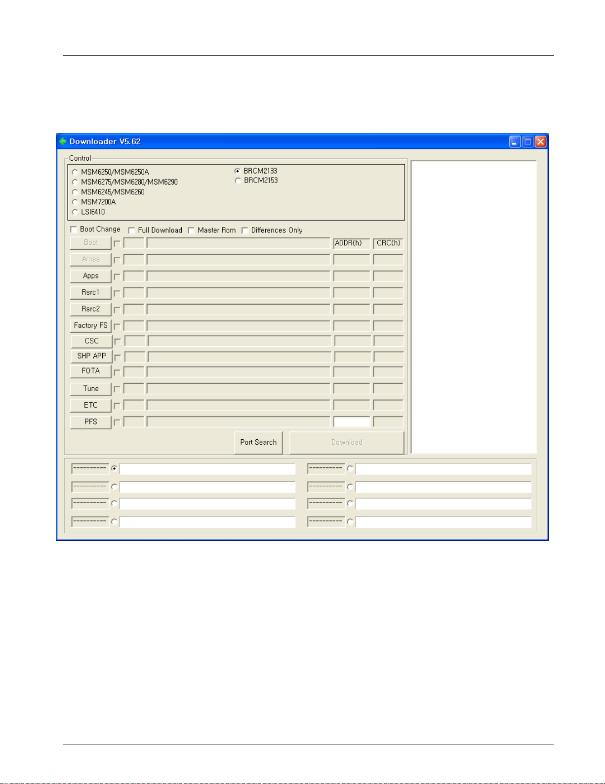
Level1Repair
Select the
2.
BRCM2133".
"
as Control.
6-3
SAMSUNG Proprietary-Contents may change without notice
This Document can not be used without Samsung's authorization
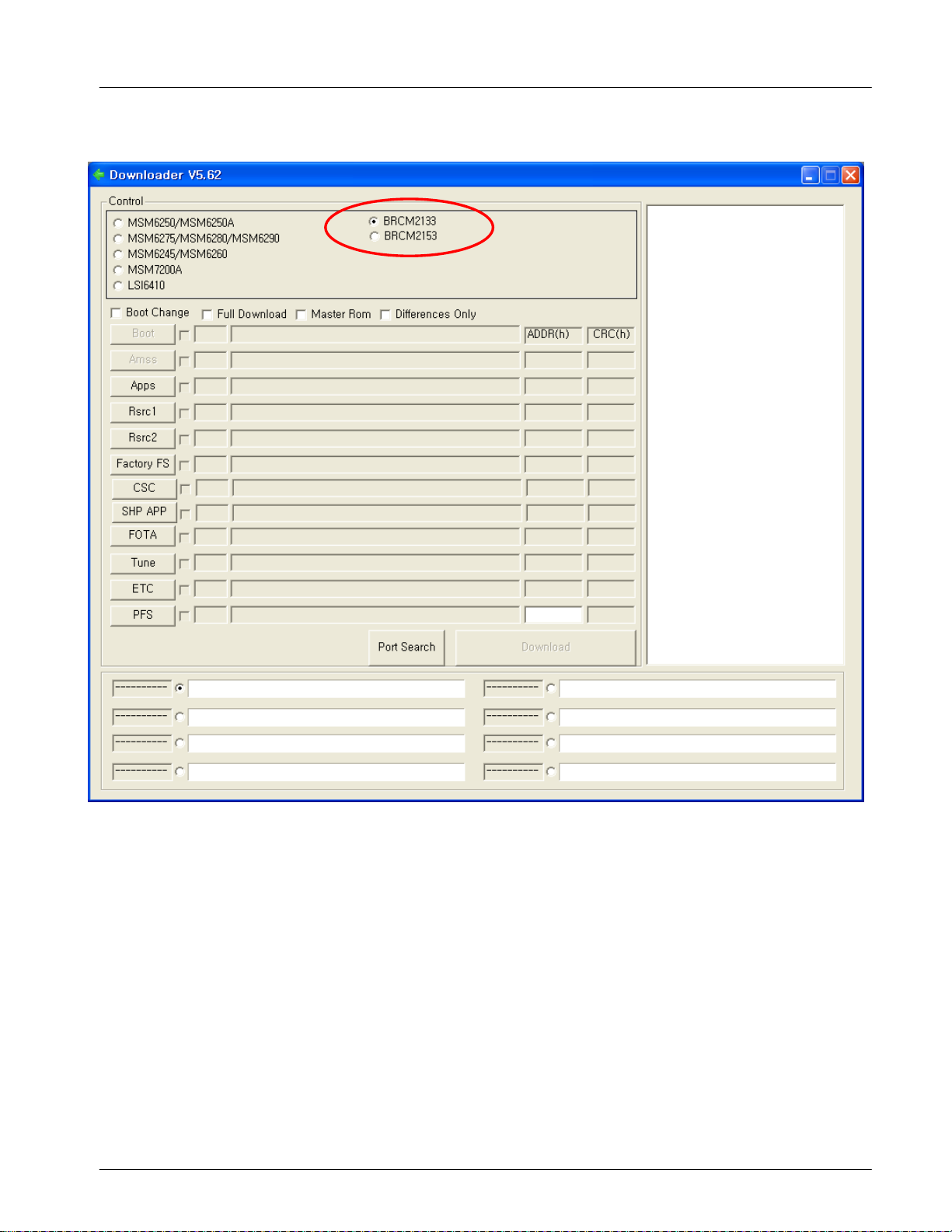
Level1Repair
Select the Full Download.
3.
6-4
SAMSUNG Proprietary-Contents may change without notice
This Document can not be used without Samsung's authorization
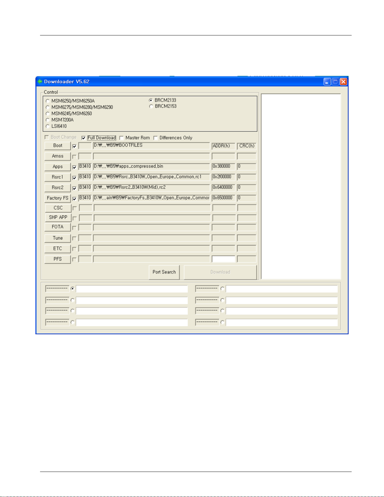
Level1Repair
Load the file of Boot, Amss, Apps, Rsrc
4.
you saved the binary files.
Rsrc2, Factory FS from the folder that
1.
6-5
SAMSUNG Proprietary-Contents may change without notice
This Document can not be used without Samsung's authorization
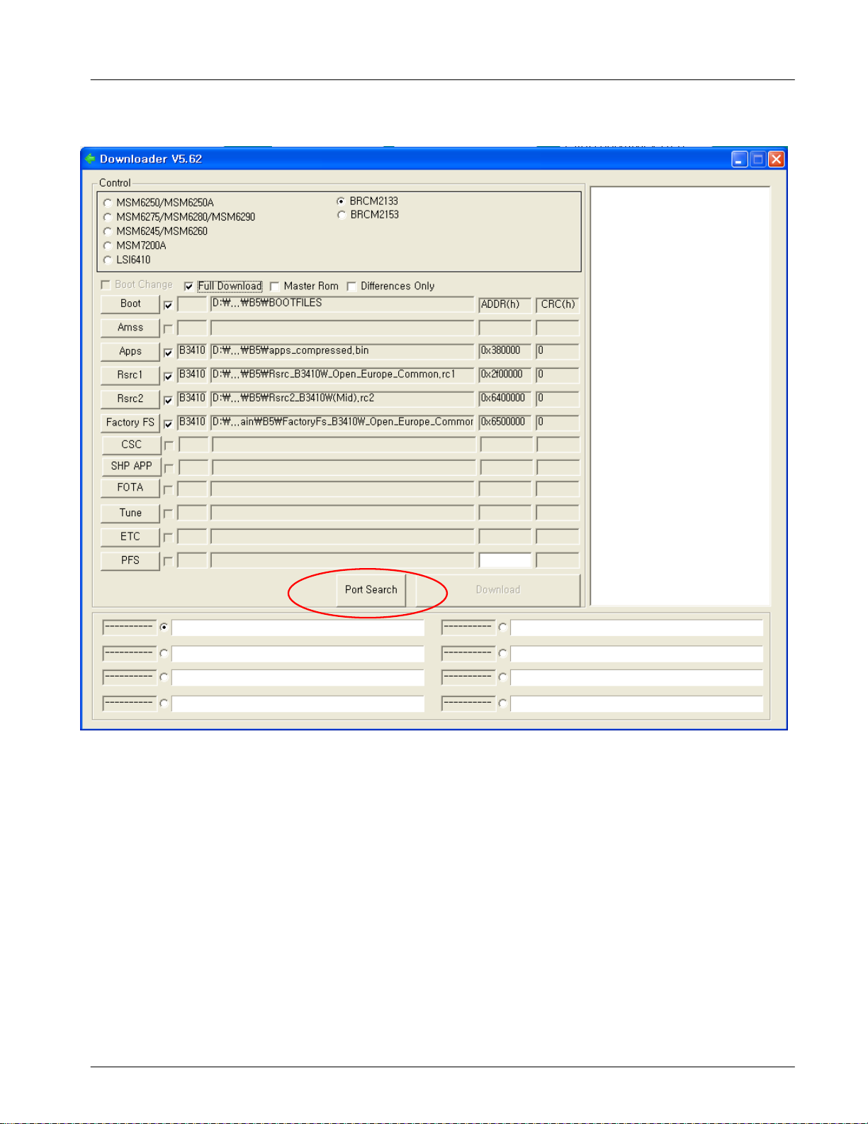
Level1Repair
Click the
5.
Port Search
button
en the download cable is connected to PC.
wh
cf. You have to set the phone asadownload mode by pressing Volume down
Camera+End key simultaneously before connecting to PC
6-6
SAMSUNG Proprietary-Contents may change without notice
This Document can not be used without Samsung's authorization
.
+
Then the down loader can search the port.
6.
Level1Repair
6-7
SAMSUNG Proprietary-Contents may change without notice
This Document can not be used without Samsung's authorization
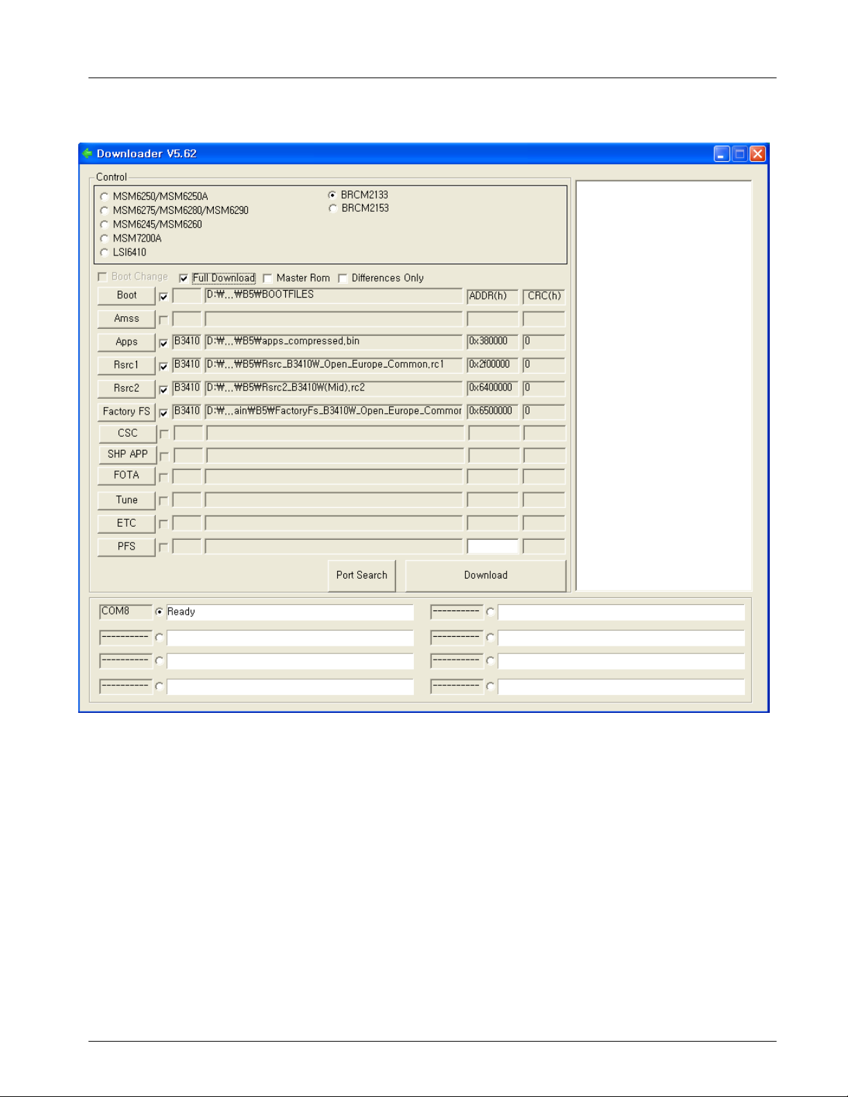
Level1Repair
Click the
7.
Download
It will start to download.
button
en the Port searched.
wh
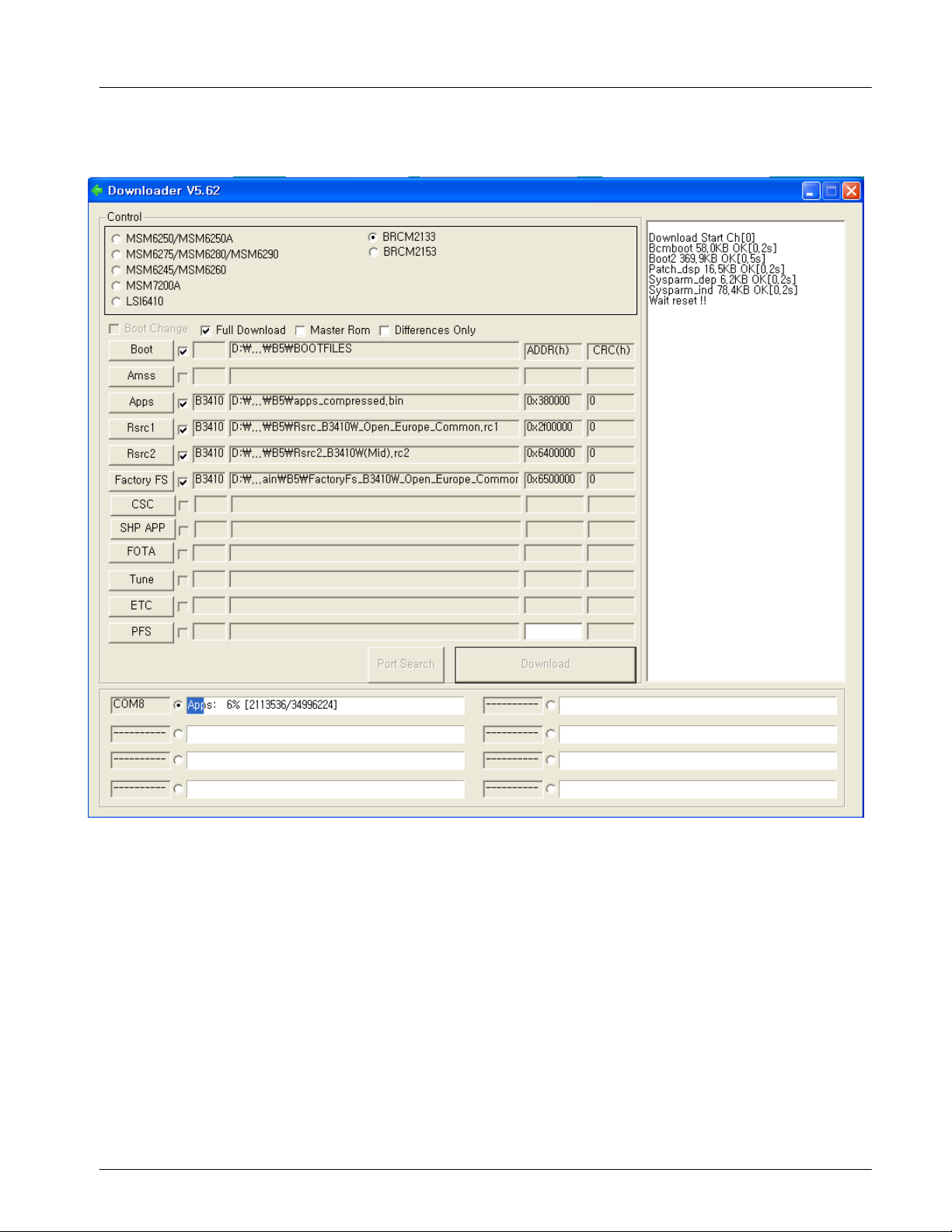
When downloading is finished successfully, there is
8.
6-8
SAMSUNG Proprietary-Contents may change without notice
This Document can not be used without Samsung's authorization
All files complete"message.
a"
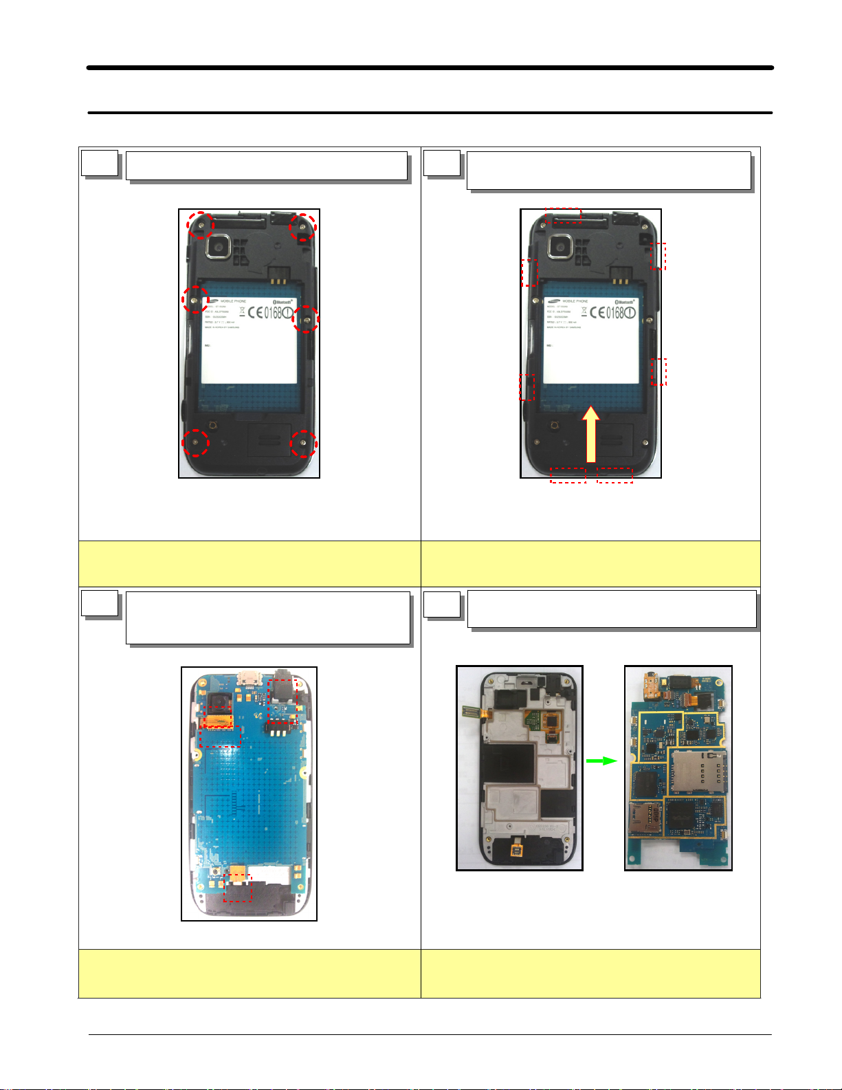
Level
7.
Disassembly
7-1.
Repair
2
1
(
1)
Unscrew the6points.
1)
Caution
Be care of scratch and molding damage.
2
(
1)
Seperate lower part of rear using
1)
decomposition tool.
Caution
Be care of scratch and molding damage.
a
Separate the LCD and Sub key Connectors
1)
3
from PBA.
Disassemble the Cam and
2)
Caution
(
Be care of damage to Connectors, Cam and
1)
phi Earjack
5
phi Earjack.
3.5
Separate the PBA ASS'Y from the FRONT
1)
4
ASS'Y.
Caution
(
Be care of scratch and molding damage.
3.
1)
Be care of damage to FPCB.
2)
7-1
SAMSUNG Proprietary-Contents may change without notice
This Document can not be used without Samsung's authorization
 Loading...