

Samsung S524LB0X91, S524LB0XB1 Datasheet

S524LB0X91/B0XB1
32K/64K-bit
Serial EEPROM
Data Sheet
OVERVIEW
The S524LB0D91/B0DB1 serial EEPROM has a 32/64 Kbits (4,096/8,192 bytes) capacity, supporting the
standard I2C™-bus serial interface. It is fabricated using Samsung’s most advanced CMOS technology. One of
its major features is a hardware-based write protection circuit for the entire memory area. Hardware-based write
protection is controlled by the state of the write-protect (WP) pin. Using one-page write mode, you can load up to
32 bytes of data into the EEPROM in a single write operation. Another significant feature of the
S524LB0D91/B0DB1 is its support for fast mode and standard mode.
FEATURES
I2C-Bus Interface
• Two-wire serial interface
• Automatic word address increment
EEPROM
• 32/64 Kbits (4,096/8,192 bytes) storage area
• 32-byte page buffer
• Typical 3-millisecond write cycle time with auto-
erase function
• Hardware-based write protection for the entire
EEPROM (using the WP pin)
• EEPROM programming voltage generated
on chip
• 1,000,000 erase/write cycles
• 100 years data retention
Operating Characteristics
• Operating voltage: 2.0 V to 5.5 V
• Operating current
— Maximum write current: < 3 mA at 5.5 V
— Maximum read current: < 500 µA at 5.5 V
— Maximum stand-by current: < 2 µA at 2.0 V
• Operating temperature range:
— – 25 °C to + 70 °C (Commercial)
— – 40 °C to + 85 °C (Industrial)
• Operating clock frequencies
— 100 kHz at standard mode
— 400 kHz at fast mode
• Electrostatic discharge (ESD)
— 5,000 V (HBM)
— 500 V (MM)
Packages
• 8-pin DIP and SOP
7-1
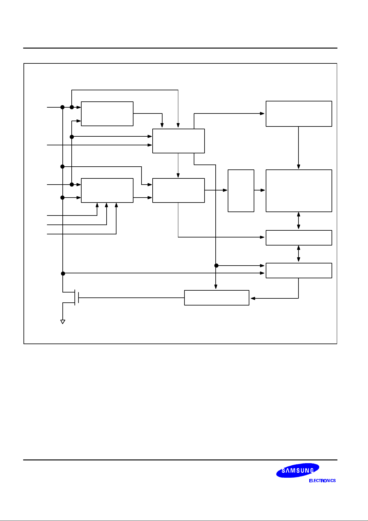
S524LB0D91/B0DB1 SERIAL EEPROM DATA SHEET
SDA
WP
SCL
A0
A1
A2
Start/Stop
Logic
Slave Address
Comparator
Control Logic
Word Address
Pointer
Row
Decoder
HV Generation
Timing Control
EEPROM
Cell Array
4,096 x 8 Bits
8,192 x 8 Bits
Column Decoder
Data Register
D
and ACK
OUT
Figure 7-1. S524LB0D91/B0DB1 Block Diagram
7-2
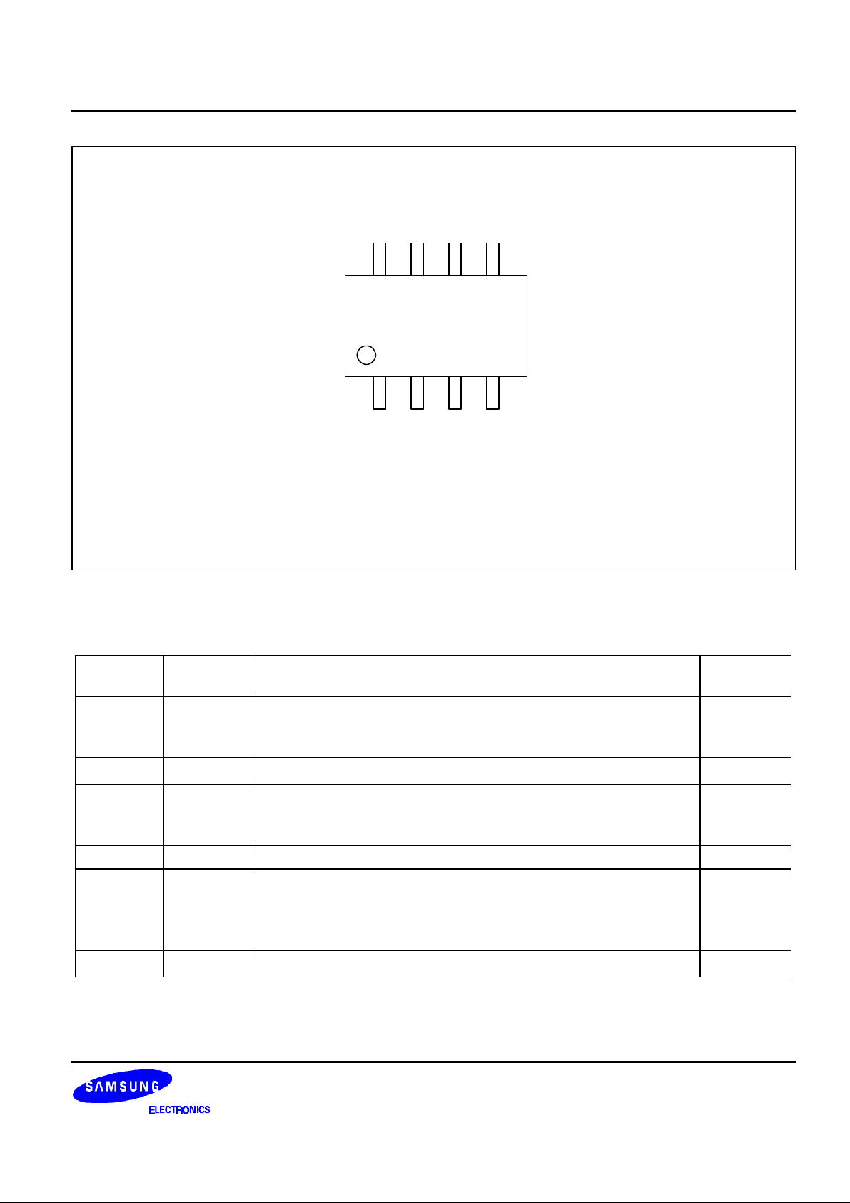
DATA SHEET S524LB0D91/B0DB1 SERIAL EEPROM
VCC WP SCL SDA
S524AB0D91/B0DB1
A0 A1 A2 VSS
NOTE: The S524AB0D91/B0DB1 is available in
8-pin DIP, SOP, and TSSOP package.
Figure 7-2. Pin Assignment Diagram
Table 7-1. S524LB0D91/B0DB1 Pin Descriptions
Name Type Description Circuit
A0, A1, A2
Input Input pins for device address selection. To configure a device
address, these pins should be connected to the VCC or V
SS
of the
device.
VSS
– Ground pin. –
SDA I/O Bi-directional data pin for the I2C-bus serial data interface. Schmitt
trigger input and open-drain output. An external pull-up resistor
must be connected to V
DD.
SCL Input Schmitt trigger input pin for serial clock input. 2
WP Input Input pin for hardware write protection control. If you tie this pin to
V
the write function is disabled to protect previously written data
CC,
in the entire memory; if you tie it to VSS, the write function is
enabled.
VCC
– Single power supply. –
Number
1
3
1
NOTE: See the following page for diagrams of pin circuit types 1, 2, and 3.
7-3
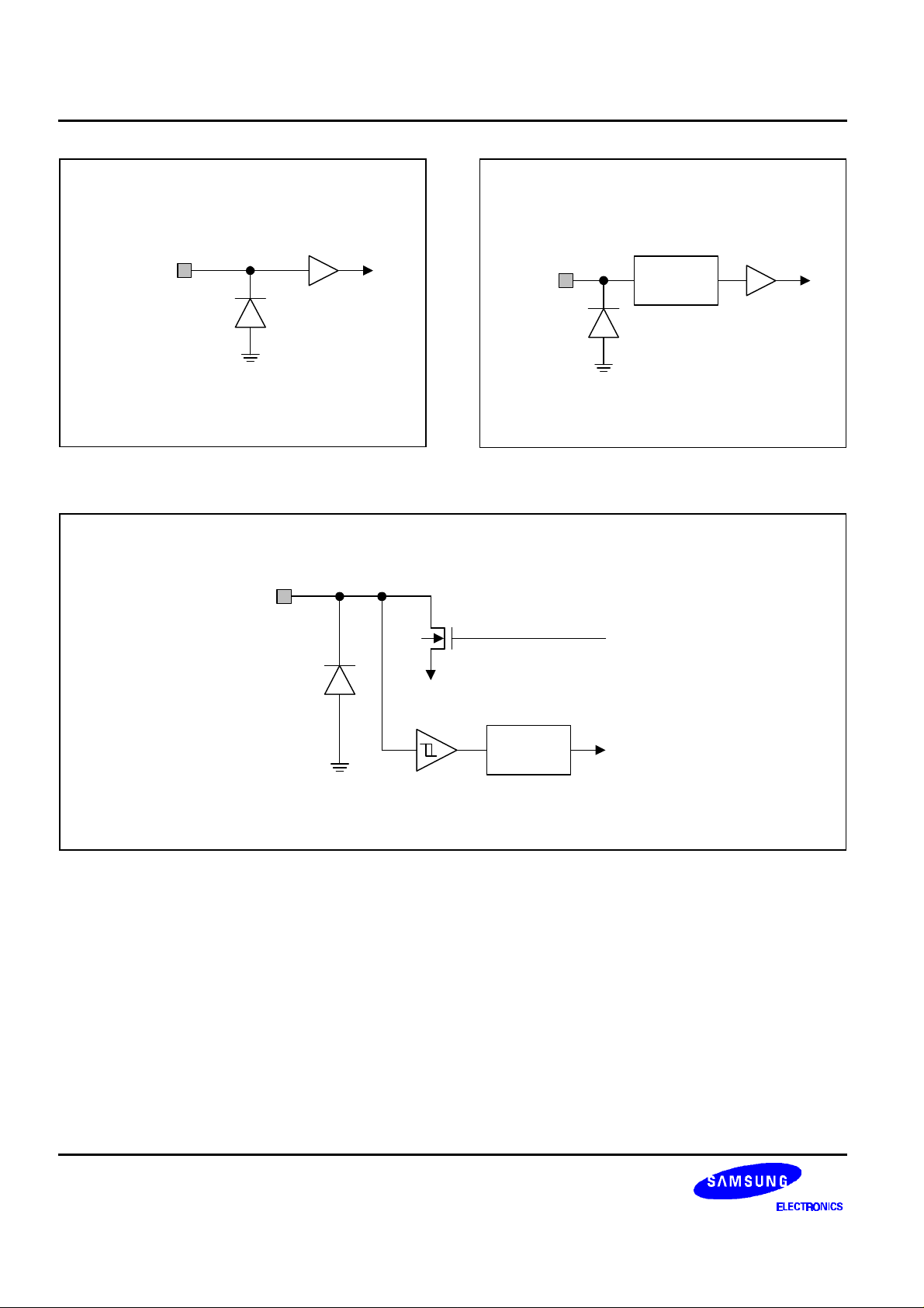
S524LB0D91/B0DB1 SERIAL EEPROM DATA SHEET
A0, A1,
A2, WP
Figure 7-3. Pin Circuit Type 1
SDA
VSS
SCL
Noise
Filter
Figure 7-4. Pin Circuit Type 2
Data Out
Noise
Filter
Figure 7-5. Pin Circuit Type 3
Data In
7-4
DATA SHEET S524LB0D91/B0DB1 SERIAL EEPROM
FUNCTION DESCRIPTION
I2C-BUS INTERFACE
The S524LB0D91/B0DB1 supports the I2C-bus serial interface data transmission protocol. The two-wire bus
consists of a serial data line (SDA) and a serial clock line (SCL). The SDA and the SCL lines must be connected
to VCC by a pull-up resistor that is located somewhere on the bus.
Any device that puts data onto the bus is defined as a “transmitter” and any device that gets data from the bus is
a “receiver.” The bus is controlled by a master device which generates the serial clock and start/stop conditions,
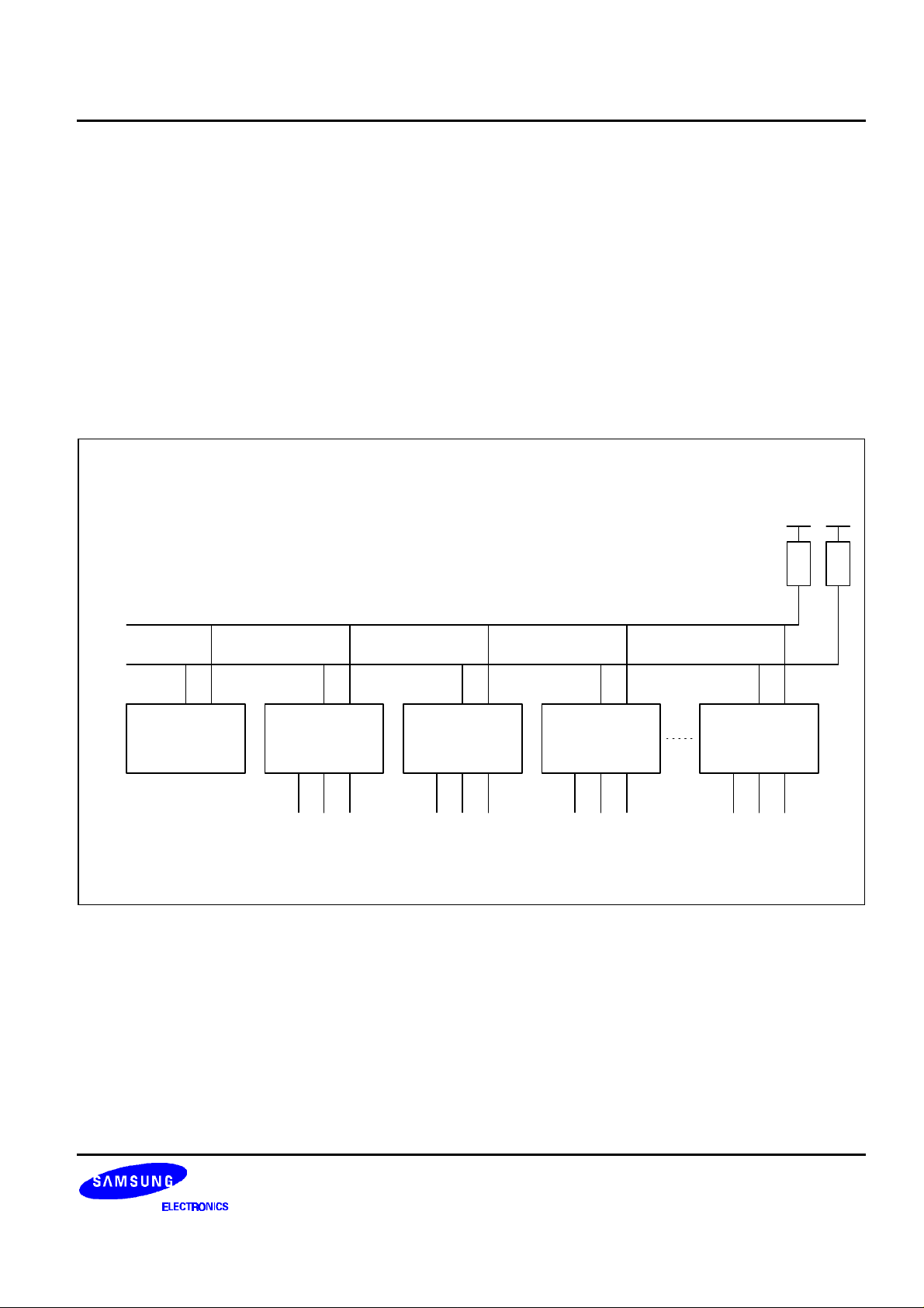
controlling bus access. Using the A0, A1, and A2 input pins, up to eight S524LB0D91/B0DB1 devices can be
connected to the same I2C-bus as slaves (see Figure 7-6). Both the master and slaves can operate as a
transmitter or a receiver, but the master device determines which bus operating mode would be active.
V
CC
V
CC
SDA
SCL
Bus Master
(Transmitter/
Receiver)
MCU
Slave 1
S524LB0D91/
B0XB1
Tx/Rx
A0 A1 A2
To VCC or V
SS
Slave 2
S524LB0D91/
B0XB1
Tx/Rx
A0 A1 A2
To VCC or V
SS
Slave 3
S524LB0D91/
B0XB1
Tx/Rx
A0 A1 A2
To VCC or V
Figure 7-6. Typical Configuration
SS
Slave 8
S524LB0D91/
B0XB1
Tx/Rx
A0 A1 A2
To VCC or V
SS
R
R
7-5
S524LB0D91/B0DB1 SERIAL EEPROM DATA SHEET
I2C-BUS PROTOCOLS
Here are several rules for I2C-bus transfers:
— A new data transfer can be initiated only when the bus is currently not busy.
— MSB is always transferred first in transmitting data.
— During a data transfer, the data line (SDA) must remain stable whenever the clock line (SCL) is High.
The I2C-bus interface supports the following communication protocols:
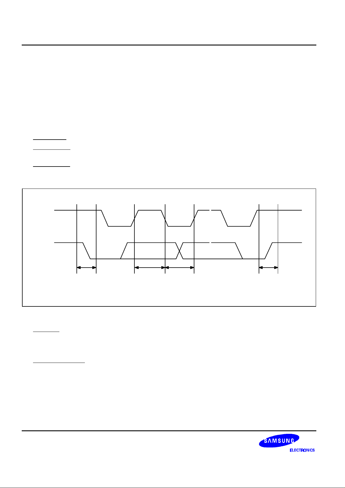
• Bus not busy: The SDA and the SCL lines remain in High level when the bus is not active.
• Start condition: A start condition is initiated by a High-to-Low transition of the SDA line while SCL remains in
High level. All bus commands must be preceded by a start condition.
• Stop condition: A stop condition is initiated by a Low-to-High transition of the SDA line while SCL remains in
High level. All bus operations must be completed by a stop condition (see Figure 7-7).
~
SCL
SDA
Start
Condition
Data or
ACK Valid
Data
Change
~
~
~
Stop
Condition
Figure 7-7. Data Transmission Sequence
• Data valid: Following a start condition, the data becomes valid if the data line remains stable for the duration
of the High period of SCL. New data must be put onto the bus while SCL is Low. Bus timing is one clock
pulse per data bit. The number of data bytes to be transferred is determined by the master device. The total
number of bytes that can be transferred in one operation is theoretically unlimited.
• ACK (Acknowledge): An ACK signal indicates that a data transfer is completed successfully. The transmitter
(the master or the slave) releases the bus after transmitting eight bits. During the 9th clock, which the master
generates, the receiver pulls the SDA line low to acknowledge that it has successfully received the eight bits
of data (see Figure 7-8). But the slave does not send an ACK if an internal write cycle is still in progress.
In data read operations, the slave releases the SDA line after transmitting 8 bits of data and then monitors
the line for an ACK signal during the 9th clock period. If an ACK is detected but no stop condition, the slave
will continue to transmit data. If an ACK is not detected, the slave terminates data transmission and waits for
a stop condition to be issued by the master before returning to its stand-by mode.
7-6
 Loading...