

Samsung S524A40X11, S524A60X51, S524A60X81, S524A40X21, S524A40X41 Datasheet
S524A40X11/40X21/
40X41/60X81/60X51
1K/2K/4K/8K/16K-bit
Serial EEPROM for Low Power
Data Sheet
OVERVIEW
The S524A40X11/40X21/40X41/60X81/60X51 serial EEPROM has a 1,024/2,048/4,096/8,192/16,384-bit
capacity, supporting the standard I2C™-bus serial interface. It is fabricated using Samsung’s most advanced
CMOS technology. It has been developed for low power and low voltage applications (1.8 V to 5.5 V). One of its
major feature is a hardware-based write protection circuit for the entire memory area. Hardware-based write
protection is controlled by the state of the write-protect (WP) pin. Using one-page write mode, you can load up to
16 bytes of data into the EEPROM in a single write operation. Another significant feature of the
S524A40X11/40X21/40X41/60X81/60X51 is its support for fast mode and standard mode.
FEATURES
I2C-Bus Interface
• Two-wire serial interface
• Automatic word address increment
EEPROM
• 1K/2K/4K/8K/16K-bit
(128/256/512/1,024/2,048-byte) storage area
• 16-byte page buffer
• Typical 3 ms write cycle time with
auto-erase function
• Hardware-based write protection for the entire
EEPROM (using the WP pin)
• EEPROM programming voltage generated
on chip
• 1,000,000 erase/write cycles
• 100 years data retention
Operating Characteristics
• Operating voltage
— 1.8 V to 5.5 V
• Operating current
— Maximum write current: < 3 mA at 5.5 V
— Maximum read current: < 200 µA at 5.5 V
— Maximum stand-by current: < 1 µA at 5.5 V
• Operating temperature range
— – 25°C to + 70°C (commercial)
— – 40°C to + 85°C (industrial)
• Operating clock frequencies
— 100 kHz at standard mode
— 400 kHz at fast mode
• Electrostatic discharge (ESD)
— 5,000 V (HBM)
— 500 V (MM)
Packages
• 8-pin DIP, SOP, and TSSOP
1-1
S524A40X11/40X21/40X41/60X81/60X51 SERIAL EEPROM DATA SHEET
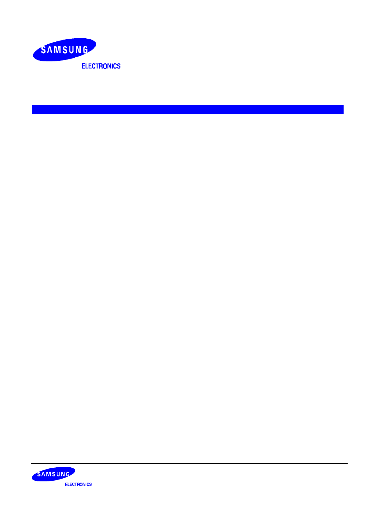
SDA
WP
SCL
A0
A1
A2
Start/Stop
Logic
Slave Address
Comparator
Control Logic
Word Address
Pointer
Row
decoder
HV Generation
Timing Control
EEPROM
Cell Array
128 x 8 bits
256 x 8 bits
512 x 8 bits
1024 x 8 bits
2048 x 8 bits
Column Decoder
Data Register
DOUT and ACK
Figure 1-1. S524A40X11/40X21/40X41/60X81/60X51 Block Diagram
1-2
DATA SHEET S524A40X11/40X21/40X41/60X81/60X51 SERIAL EEPROM
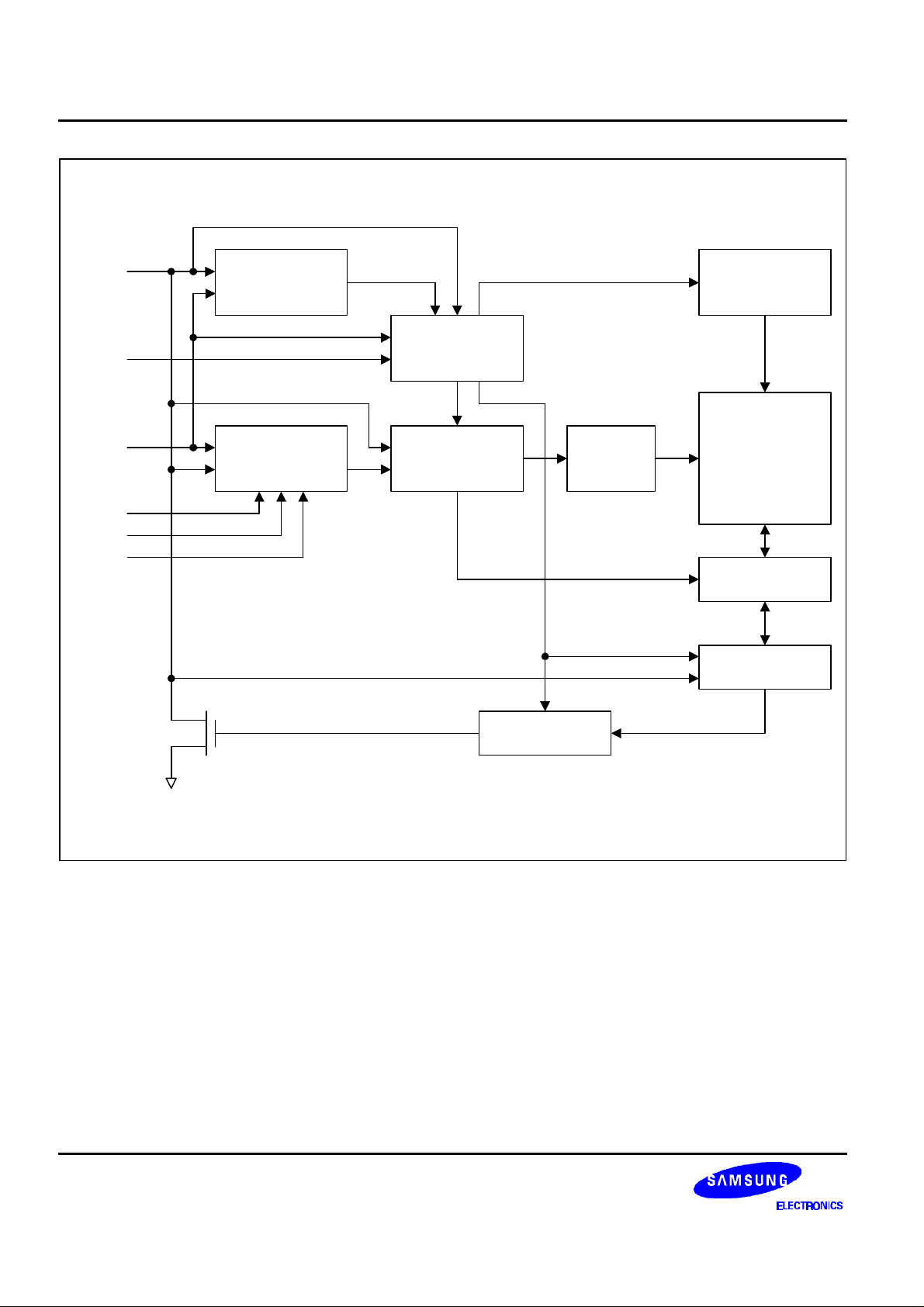
VCC WP SCL SDA
S524A40X11/40X21/
40X41/60X81/60X51
A0 A1 A2 VSS
NOTE: The S524A40X11/40X21/40X41/60X81/60X51
is available in 8-pin DIP, SOP, and TSSOP package.
Figure 1-2. Pin Assignment Diagram
Table 1-1. S524A40X11/40X21/40X41/60X81/60X51 Pin Descriptions
Name Type Description Circuit
Type
A0, A1, A2
Input Input pins for device address selection. To configure a device address,
these pins should be connected to the VCC or V
of the device.
SS
These pins are internally pulled down to VSS.
VSS
– Ground pin. –
SDA I/O Bi-directional data pin for the I2C-bus serial data interface. Schmitt
trigger input and open-drain output. An external pull-up resistor must
be connected to V
Typical values for this pull-up resistor are 4.7 kΩ
CC.
(100 kHz) and 1 kΩ (400 kHz).
SCL Input Schmitt trigger input pin for serial clock input. 2
WP Input
Input pin for hardware write protection control. If you tie this pin to V
CC,
the write function is disabled to protect previously written data in the
entire memory; if you tie it to VSS, the write function is enabled.
This pin is internally pulled down to VSS.
1
3
1
VCC
NOTE: See the following page for diagrams of pin circuit types 1, 2, and 3.
– Single power supply. –
1-3
S524A40X11/40X21/40X41/60X81/60X51 SERIAL EEPROM DATA SHEET
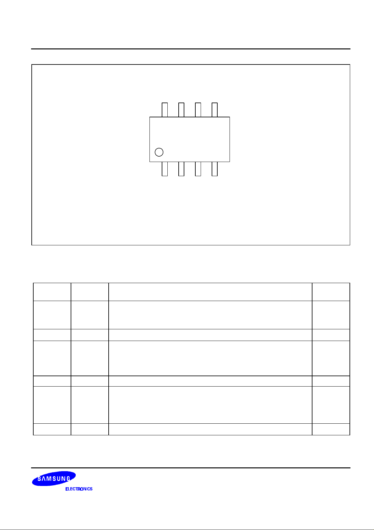
A0, A1,
A2, WP
Figure 1-3. Pin Circuit Type 1
SDA
VSS
SCL
Noise
Filter
Figure 1-4. Pin Circuit Type 2
Data Out
Noise
Filter
Figure 1-5. Pin Circuit Type 3
Data In
1-4
DATA SHEET S524A40X11/40X21/40X41/60X81/60X51 SERIAL EEPROM
FUNCTION DESCRIPTION
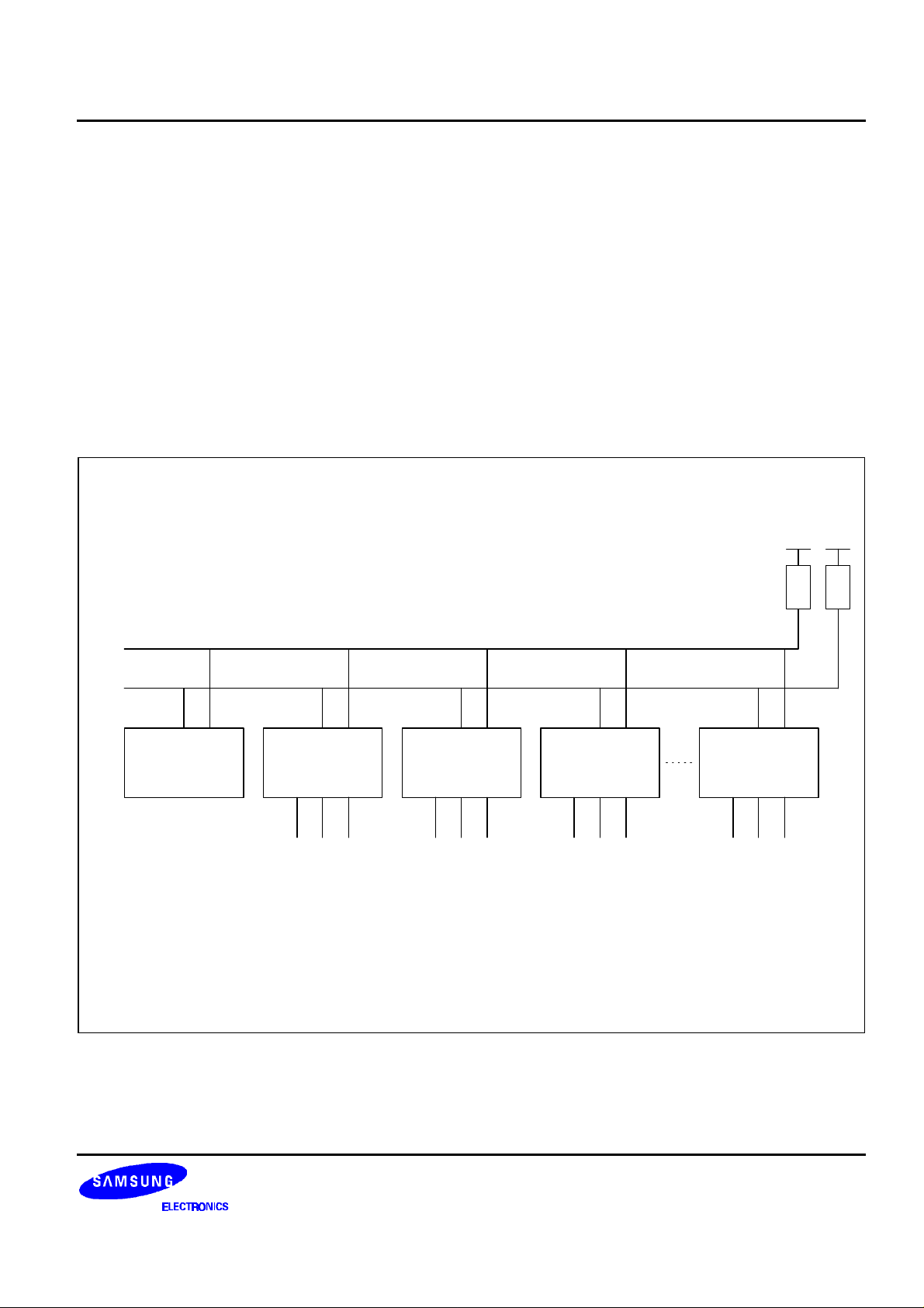
I2C-BUS INTERFACE
The S524A40X11/40X21/40X41/60X81/60X51 supports the I2C-bus serial interface data transmission protocol.
The two-wire bus consists of a serial data line (SDA) and a serial clock line (SCL). The SDA and the SCL lines
must be connected to VCC by a pull-up resistor that is located somewhere on the bus.
Any device that puts data onto the bus is defined as the “transmitter” and any device that gets data from the bus
is the “receiver.” The bus is controlled by a master device which generates the serial clock and start/stop
conditions, controlling bus access. Using the A0, A1, and A2 input pins, up to eight S524A40X11/40X21 (four
S524A40X41, two for S524A60X81, one for S524A60X51) devices can be connected to the same I2C-bus as
slaves (see Figure 1-6). Both the master and slaves can operate as transmitter or receiver, but the master device
determines which bus operating mode would be active.
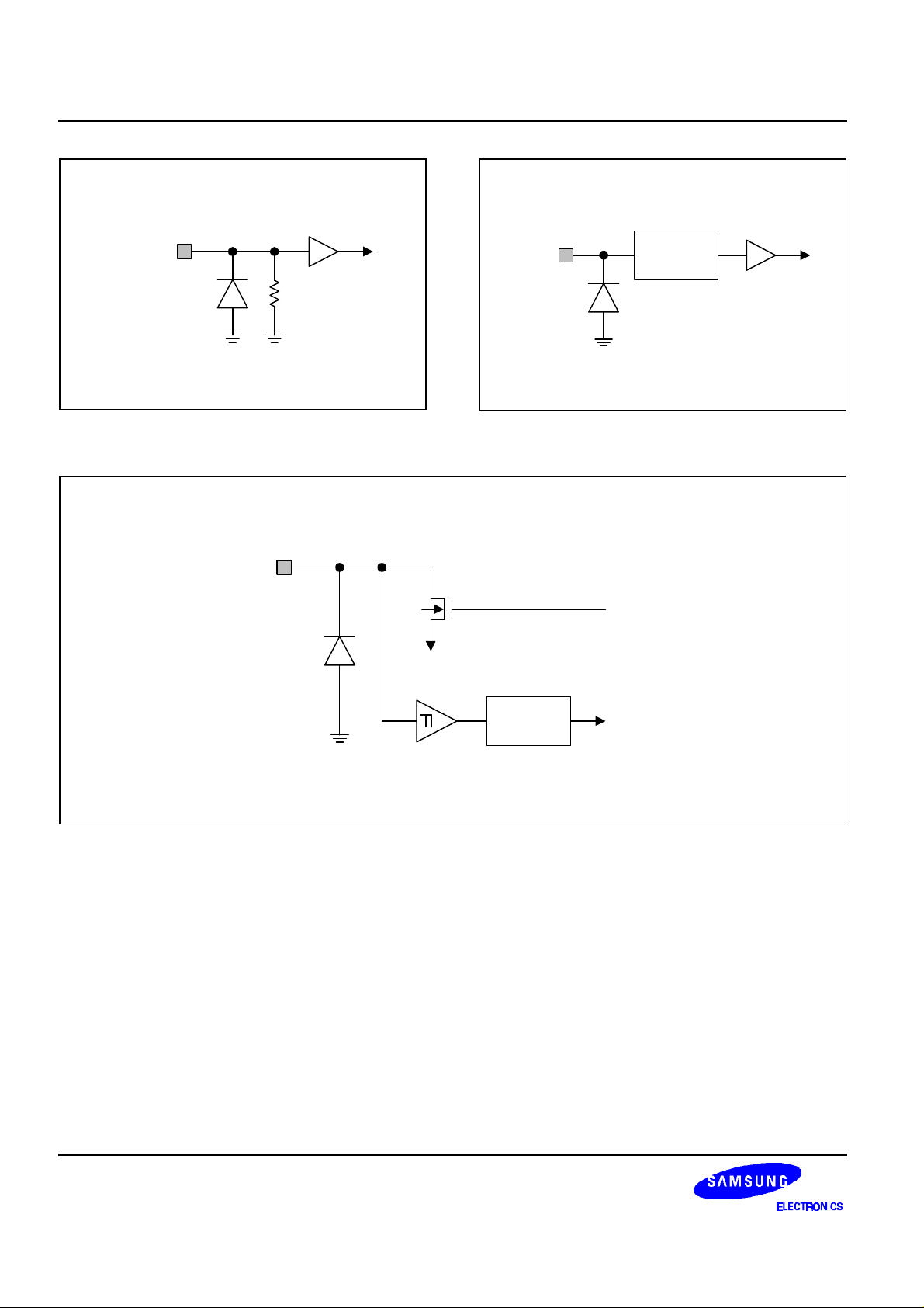
V
CC
V
CC
SDA
SCL
Bus Master
(Transmitter/
Receiver)
MCU
Slave 1
S524A40X21
Tx/Rx
A0 A1 A2
To VCC or V
NOTES:
1. The A0 does not affect the device address of the S524A40X41.
2. The A0, A1 do not affect the device address of the S524A60X81.
3. The A0, A1, and A2 do not affect the device address of the S524A60X51.
SS
Slave 2
S524A40X21
Tx/Rx
A0 A1 A2
To VCC or V
SS
Slave 3
S524A40X21
Tx/Rx
A0 A1 A2
To VCC or V
SS
Slave 8
S524A40X21
Tx/Rx
A0 A1 A2
To VCC or V
SS
R
R
Figure 1-6. Typical Configuration (16 Kbits of Memory on the I2C-Bus)
1-5
 Loading...