

Page 1
S3FM02G
Evaluation Board
Revision 1.00
February 2011
UUsseerr''ss GGuuiiddee
2011 Samsung Electronics Co., Ltd. All rights reserved.
Page 2

Important Notice
The information in this publication has been carefully
checked and is believed to be entirely accurate at the
time of publication. Samsung assumes no
responsibility, however, for possible errors or
omissions, or for any consequences resulting from the
use of the information contained herein.
Samsung reserves the right to make changes in its
products or product specifications with the intent to
improve function or design at any time and without
notice and is not required to update this
documentation to reflect such changes.
This publication does not convey to a purchaser of
semiconductor devices described herein any license
under the patent rights of Samsung or others.
Samsung makes no warranty, representation, or
guarantee regarding the suitability of its products for
any particular purpose, nor does Samsung assume
any liability arising out of the application or use of any
product or circuit and specifically disclaims any and all
liability, including without limitation any consequential
or incidental damages.
Copyright
2011 Samsung Electronics Co., Ltd.
"Typical" parameters can and do vary in different
applications. All operating parameters, including
"Typicals" must be validated for each customer
application by the customer's technical experts.
Samsung products are not designed, intended, or
authorized for use as components in systems intended
for surgical implant into the body, for other
applications intended to support or sustain life, or for
any other application in which the failure of the
Samsung product could create a situation where
personal injury or death may occur.
Should the Buyer purchase or use a Samsung product
for any such unintended or unauthorized application,
the Buyer shall indemnify and hold Samsung and its
officers, employees, subsidiaries, affiliates, and
distributors harmless against all claims, costs,
damages, expenses, and reasonable attorney fees
arising out of, either directly or indirectly, any claim of
personal injury or death that may be associated with
such unintended or unauthorized use, even if such
claim alleges that Samsung was negligent regarding
the design or manufacture of said product.
All rights reserved. No part of this publication may be reproduced, stored in a retrieval system, or transmitted in
any form or by any means, electric or mechanical, by photocopying, recording, or otherwise, without the prior
written consent of Samsung Electronics.
Samsung Electronics Co., Ltd.
San #24 Nongseo-Dong, Giheung-Gu
Yongin-City, Gyeonggi-Do, Korea 446-711
Contact Us:
TEL: (82)-(31)-209-4956
FAX: (82)-(31)-209-6494
Home Page:
http://www.samsungsemi.com
Page 3
Revision History
Revision No.
Date
Description
Author(s)
1.00
Feb. 08, 2011
Initial draft
Juil Kim
Page 4

Table of Contents
1 S3FM02G DESCRIPTION ............................................................................. 1-1
1.1 Instruction to S3FM02G ........................................................................................................................... 1-1
1.2 S3FM02G Block Diagram ........................................................................................................................ 1-2
1.3 System Requirements .............................................................................................................................. 1-3
1.3.1 Software Requirements .................................................................................................................... 1-3
1.3.2 Hardware Requirements ................................................................................................................... 1-3
1.4 Board Components .................................................................................................................................. 1-3
2 EVB DESCRIPTION ...................................................................................... 2-1
2.1 Configuration ............................................................................................................................................ 2-1
2.2 Detailed Block Configurations .................................................................................................................. 2-2
2.2.1 Power Generator Block .................................................................................................................... 2-2
2.2.2 Mode Set Block ................................................................................................................................. 2-3
2.2.3 CAN Block ........................................................................................................................................ 2-4
2.2.3.1 Features .................................................................................................................................. 2-4
2.2.3.2 Block Description .................................................................................................................... 2-5
2.2.4 ENC Block ........................................................................................................................................ 2-6
2.2.4.1 Features .................................................................................................................................. 2-6
2.2.4.2 Block Description .................................................................................................................... 2-7
2.2.5 USART Block (LIN / RS-485 Include) ............................................................................................... 2-8
2.2.5.1 Features .................................................................................................................................. 2-8
2.2.5.2 Block Description .................................................................................................................... 2-9
2.2.6 SSP Block ....................................................................................................................................... 2-11
2.2.6.1 Features ................................................................................................................................ 2-11
2.2.6.2 Block Description .................................................................................................................. 2-12
2.2.7 I2C Block ........................................................................................................................................ 2-13
2.2.7.1 Features ................................................................................................................................ 2-13
2.2.7.2 Block Description .................................................................................................................. 2-13
2.2.8 ADC Block ...................................................................................................................................... 2-14
2.2.8.1 Features ................................................................................................................................ 2-14
2.2.8.2 Block Description .................................................................................................................. 2-14
2.2.9 OP-AMP Block ................................................................................................................................ 2-15
2.2.9.1 Features ................................................................................................................................ 2-15
2.2.9.2 Block Description .................................................................................................................. 2-15
2.2.10 LCD Block ..................................................................................................................................... 2-16
2.2.10.1 Features .............................................................................................................................. 2-16
2.2.10.2 Block Description ................................................................................................................ 2-17
2.2.11 Other Blocks ................................................................................................................................. 2-18
2.2.11.1 Buzzer ................................................................................................................................. 2-18
2.2.11.2 LED Display ........................................................................................................................ 2-18
2.2.11.3 Wake Up ............................................................................................................................. 2-19
2.3 Total Blocks Unit & Jumper Summary ................................................................................................... 2-20
2.3.1 Each Blocks .................................................................................................................................... 2-20
2.3.1.1 Switch .................................................................................................................................... 2-21
Page 5

List of Figures
Figure Title Page
Number Number
Figure 1-1 Block Diagram ................................................................................................................................... 1-2
Figure 2-1 Board Configuration .......................................................................................................................... 2-1
Figure 2-2 Power Generator Block ..................................................................................................................... 2-2
Figure 2-3 Mode Set Block ................................................................................................................................. 2-3
Figure 2-4 CAN Block Description ..................................................................................................................... 2-5
Figure 2-5 Encoder Block Description ................................................................................................................ 2-7
Figure 2-6 USART Block Description ............................................................................................................... 2-10
Figure 2-7 SSP Block Description .................................................................................................................... 2-13
Figure 2-8 I2C Block Description ..................................................................................................................... 2-13
Figure 2-9 ADC Block Description ................................................................................................................... 2-14
Figure 2-10 OP-AMP Block Description ........................................................................................................... 2-15
Figure 2-11 LCD Block Description .................................................................................................................. 2-17
Figure 2-12 Buzzer Block Description .............................................................................................................. 2-18
Figure 2-13 LED Block Description .................................................................................................................. 2-18
Figure 2-14 Wake Up Block Description .......................................................................................................... 2-19
Page 6

List of Tables
Table Title Page
Number Number
Table 2-1 ENC Pin Description .......................................................................................................................... 2-6
Table 2-2 USART Pin Description ...................................................................................................................... 2-8
Page 7
S3FM02G_USER'S GUIDE_REV 1.00 1 S3FM02G DESCRIPTION
1 S3FM02G Description
1.1 Instruction to S3FM02G
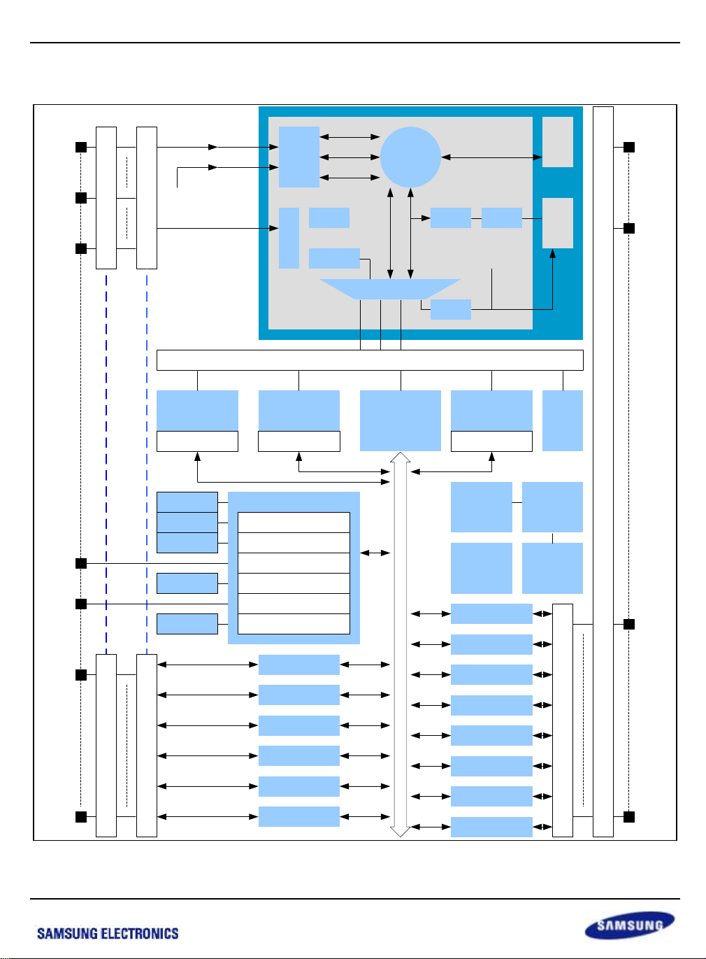
S3FM02G is a family of cost-effective and high-performance microcontrollers with Cortex-M3 designed by
Advanced RISC Machines (ARM). This Microcontroller unit (MCU) applies to inverter motor control within the
home appliance applications.
ARM Cortex-M3 Core
Built-in up to 384 Kbytes Program Flash Memory
Built-in up to 16 Kbytes Data Flash
Internal up to 24 Kbytes SRAM for stack, data memory, or cod memory
Operating temperature: –40 to 85C
Operating voltage range: 2.7 to 5.5V
Interrupt controller: Dynamically reconfigurable Nested Vectored Interrupt Controller (NVIC)
Clock and Power Controller (CM)
10-ch DMA Controller (DMAC)
Watch-Dog Timer (WDT)
8-ch 16-bit Timer/Counters (TC)
32-bit Free-Running Timer (FRT)
8-ch 16-bit PWM
2-ch 16-bit Encoder Counter (ENC)
2-ch 6-Phase Inverter Motor Controller (IMC)
2-ch I2C, 2-ch SSP, 2-ch CAN and 4-ch USART
12-bit ADC (4 channels with OP-AMP)
10-bit ADC
5-ch OP-AMP
4com. 40seg. LCD Controller (LCDC)
Support Normal, High-speed, IDLE, and STOP mode
1-1
Page 8
S3FM02G_USER'S GUIDE_REV 1.00 1 S3FM02G DESCRIPTION
CM3
Core
Interrupts
sleep
debug
N
V
I
V
S
W
J
D
P
Systick
AHB-AP
Inst
Data
DWP ITM
APB
I-Code
D-Code
S-BUS
Cortex-M3
Cortex-M3
APB
E
T
M
T
P
I
U
INTNMI
INTISR
NMI
I/O conf
GPIO
JTAG/SWDBG
AHB Bus Matrix
Program Flash
384KB
PF Controller
Data Flash
16KB
DF Controller
SRAM
24KB
SRAM Controller
AHB2APB
DMA
Con.
CM
IVC Controller
PLLCLK (8 ~ 75MHz)
EMCLK (4 ~ 8MHz)
IMCLK (8/16/20MHz)
ESCLK (32.768KHz)
ISCLK (32.768KHz)
I/O conf
GPIO
PLL
IMOSC20
IMOSC16
ISOSC
IVC
WDT
12-BIT
ADC0
12-BIT
ADC0
10-BIT
ADC0
5ch
OP-AMP
ADC 0/1
Controller
I/O conf
GPIO
OP-AMP
Controller
FRT
8-ch
Timer/Counter
8ch PWM
4ch USART
2ch SSP
2ch I2C
2ch IMC
2ch ENC
2ch CAN
4 com x 40 seg
LCD Controller
From CM
STT
1.2 S3FM02G Block Diagram
1-2
Figure 1-1 Block Diagram
Page 9
S3FM02G_USER'S GUIDE_REV 1.00 1 S3FM02G DESCRIPTION
1.3 System Requirements
This section describes the hardware and software system requirements
1.3.1 Software Requirements
Windows NT version 4.0 , Window 95 or higher for using Multi-ICE, the debugger
1.3.2 Hardware Requirements
S3FM02G EVB Board set
Main EVB board
Power to supply DC 7 to 12V (recommend:12V)
For running the Multi-ICE server:
200MHz Pentium PC
32MB RAM for Windows95, or 64MB RAM for Windows NT
Parallel Port
1.4 Board Components
The board consists of:
32-bit RISC ARM CortexTM-M3 Core : Micro controller – S3FM02G
o ETM function embedded with ARM CortexTM-M3
o SWD (Serial Wire Debug) and JTAG Debugging Solution
Memory:
o Serial EEPROM: SSP8 (8 Kbytes 8-bit) , SSP16 (4 Kbytes 16-bit), IIC (16 Kbytes 8-bit)
Serial communication lines:
o 2 CAN (IOS 11898): 9 pin D-sub (male)
o 1 ENC: 15 pin D-sub (female)
o 2 UART (RS-232): 9 pin D-sub (female)
o 2 LIN (ISO 9141): 3 pin Terminal Block (CCP3.5)
o 1 RS-485: 3pin Terminal Block (CCP3.5)
Function blocks interfaces:
o 1 Buzzer
o 6 LED (Power(2), Port signal(4) )
o 6 Switch (Power, RESET, Wake up(4) )
o Jumper & Header pin (each Blocks)
1-3
Page 10
S3FM02G_USER'S GUIDE_REV 1.00 1 S3FM02G DESCRIPTION
Power Supply:
o 3.3V / 5V Output regulator
o DC power connector (7 to 12V)
Clocks:
o 4MHz or 8MHz (External main clock)
o Load capacitor: 15pF to 30pF (recommend: Default 22pF)
Debugging Method:
o A standard 20-pin JTAG interface connector
o Cortex debug connector (5 2 1.27mm header (male))
o Cortex debug + ETM connector (10 2 1.27mm header (male))
Display:
o Enable 4com/40seg LCD (22 2 2.54mm header (male))
1-4
Page 11
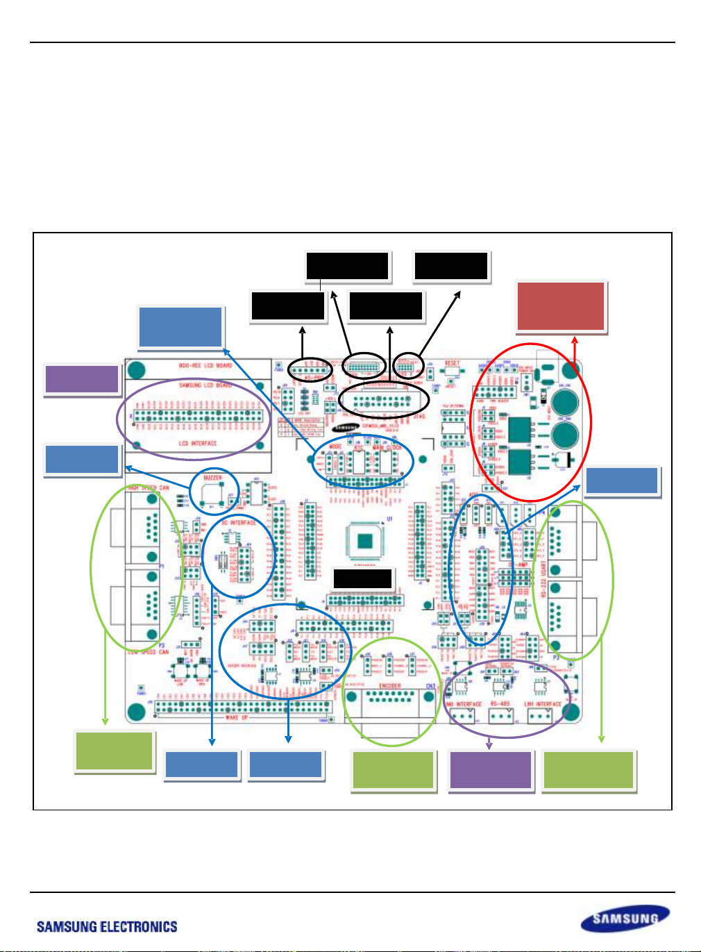
S3FM02G_USER'S GUIDE_REV 1.00 2 EVB DESCRIPTION
JTAG
CORTEX
DEBUG
CORTEX
DEBUG+ETM
AS -PRO
S3FM02G
POWER
Supply
MODE set
& Clock
CAN Block
Connector
USART Block
Connector
ENC Block
Connector
LIN & RS -
485
Terminal
LCD
SSP BlockI2C Block
BUZZER
ADC Block
2 EVB Description
2.1 Configuration
Figure 2-1 Board Configuration
2-1
Page 12
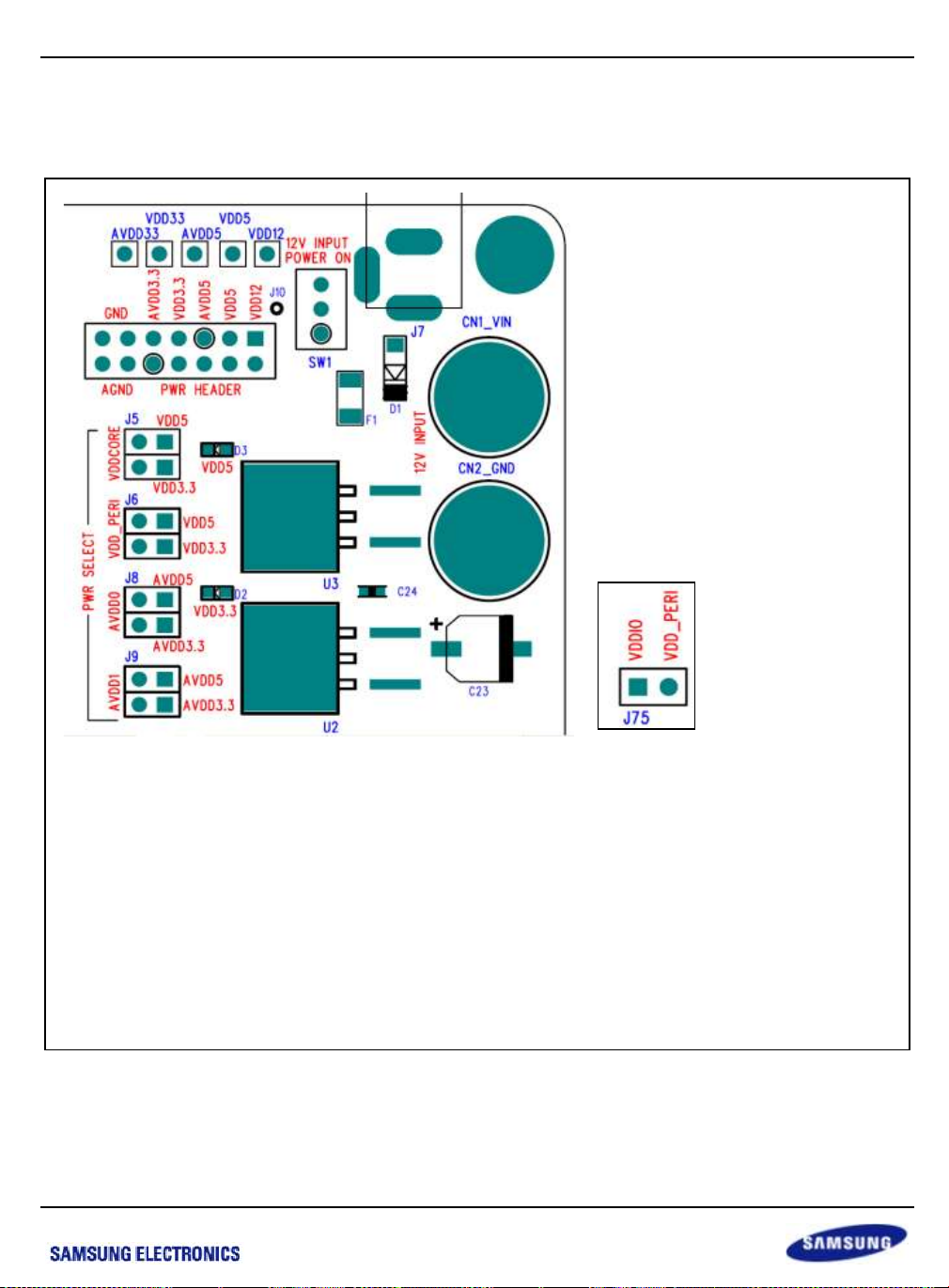
S3FM02G_USER'S GUIDE_REV 1.00 2 EVB DESCRIPTION
1. CN1,CN2,J7: Power Supply Connector
CN1: VIN / CN2 : GND
J7: DC adapter connector
2. U2,U3: 1.5A Low Drop Positive:
Voltage Regulator
3.3V(U2) / 5V(U3) fixed
D2PAK package
3. J5,J6,J8,J9: Jumper Setting for S3FM02G Power Block
J5: S3FM02Gs
VDDCORE Voltage level selection (3.3V or 5V)
J5: S3FM02Gs VDDIO Voltage level selection (3.3V or 5V)
J5: S3FM02Gs AVDD0 Voltage level selection (3.3V or 5V)
J5: S3FM02Gs AVDD1 Voltage level selection (3.3V or 5V)
4. D2,D3: Power Display LED
D2: 3.3V Display (red color) / D3 : 5V Display (green color)
5. SW1: Power Input [ON/OFF] toggle Switch ([J7 / CN] Share a switch)
6. J10: Reserve Power Pin Header
2.2 Detailed Block Configurations
2.2.1 Power Generator Block
Figure 2-2 Power Generator Block
2-2
Page 13
S3FM02G_USER'S GUIDE_REV 1.00 2 EVB DESCRIPTION
PCB TOP
PCB Bottom
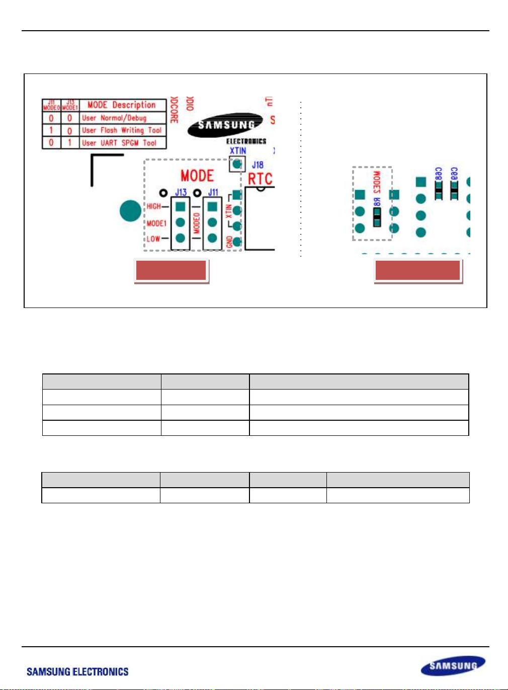
J13 (MODE1)
J11 (MODE0)
Mode Description
0(low)
0(low)
User Normal / Debug
0(high)
1(high)
User Flash Writing Tool
1(low)
0(low)
User UART SPGM Tool
R8 (MODE2)
J13 (MODE1)
J11 (MODE0)
Mode Description
1(high)
0(low)
1(high)
SCAN Mode (Test)
2.2.2 Mode Set Block
Figure 2-3 Mode Set Block
J11/J13: Jumper Setting
R8: MODE 2 Connect GND
2-3
Page 14
S3FM02G_USER'S GUIDE_REV 1.00 2 EVB DESCRIPTION
2.2.3 CAN Block
2.2.3.1 Features
Supports CAN protocol version 2.0 part A and B
Bit rates up to 1 Mbit/s
32 Message Objects
Each Message Object has its own identifier mask
Programmable FIFO mode (concatenation of Message Objects)
Maskable interrupt
Disabled Automatic Retransmission mode for Time Triggered CAN applications
Programmable loop-back mode for self-test operation
Power management block and wake up mode allowing optimization of power consumption
CAN_TX output pin configurable in open drain allowing connection without external transceiver
2-4
Page 15
S3FM02G_USER'S GUIDE_REV 1.00 2 EVB DESCRIPTION
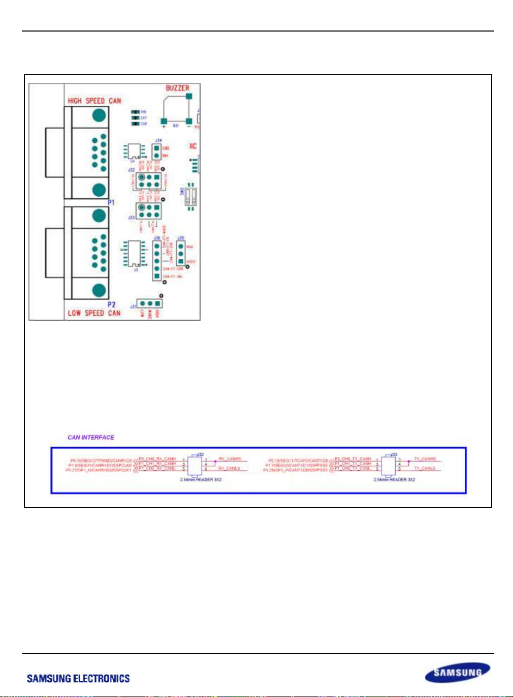
1. U4,U5: CAN Transceiver (U4 - high speed / U5 - low speed)
2. P1,P2: 9pin D-sub connector (P1 - low speed / P2 - low speed)
3. J32: Jumper Setting (Receiver)
1-2 closed: Connect RXD to P0.19 (high speed CAN_RX [CH0])
3-4 closed: Connect RXD to P1.6 (high speed CAN_RX [CH1])
5-6 closed: Connect RXD to P1.27 (low speed CAN_RX[CH0])
4. J33: Jumper Setting (Transmitter)
1-2 closed: Connect TXD to P0.18 (high speed CAN_TX [CH0])
3-4 closed: Connect TXD to P1.7 (high speed CAN_TX [CH1])
5-6 closed: Connect TXD to P1.28 (high speed CAN_TX [CH0])
5. J34: Jumper Setting (Mode Control input)
Closed: CAN Transceiver standard mode (Default close)
6. J35: Jumper Setting (Battery voltage)
1-2 Closed: VDDIN 12V input
2-3 Closed: CAN bus line input
7. J36: Low speed CAN mode select (2.54mm 5pin header)
1. INH
2. NERR
3. STB (low active)
4. EN
5. WAKE (low active)
The J36 Headers isn’t connect with ports.
If want connect to ports please use of jumper cable.
2.2.3.2 Block Description
Figure 2-4 CAN Block Description
2-5
Page 16
S3FM02G_USER'S GUIDE_REV 1.00 2 EVB DESCRIPTION
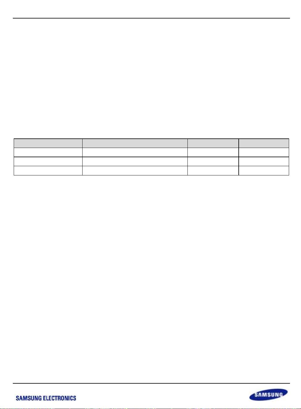
Pin Name
Function
I/O Type
Comments
PHASEA[1:0]
Phase A input
I
–
PHASEB[1:0]
Phase B input
I
–
PHASEZ[1:0]
Phase Z input
I
–
2.2.4 ENC Block
2.2.4.1 Features
Three input signals: PHASEA, PHASEB and PHASEZ
Two 16-bit up/down counters: Position Counter (PCR) and Speed Counter (SPCR)
Capture function support for slow rotating: Phase a Capture (PACDR) and Phase B Capture (PBCDR)
Filter in the PHASEZ and edge selector for PHASEZ
Up to 2 channels
Up / Down counter
Table 2-1 ENC Pin Description
2-6
Page 17
S3FM02G_USER'S GUIDE_REV 1.00 2 EVB DESCRIPTION
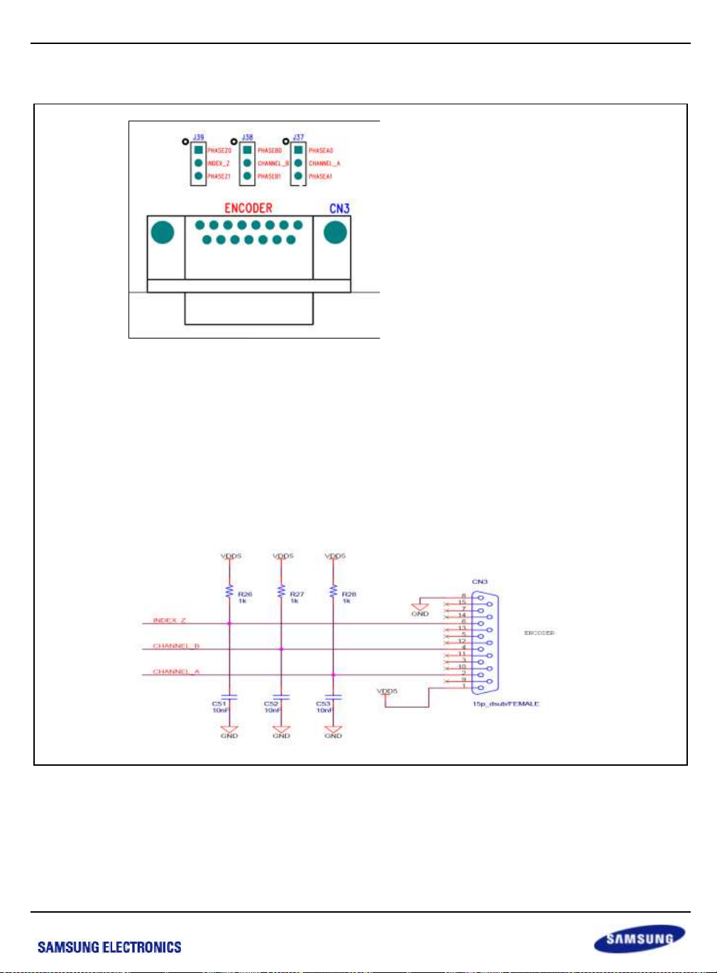
à CN3: 15pin D-sub(female)
1. CN3: 15pin D-sub(female)
1-2 closed: Connect [Channel A] to P2.23 (CH0)
2-3 closed: Connect [Channel A] to P0.29 (CH1)
2. J38: Jumper Setting (Channel B)
1-2 closed: Connect [Channel B] to P2.24 (CH0)
2-3 closed: Connect [Channel B] to P0.30 (CH1)
3. J39: Jumper Setting (Index Z)
1-2 closed: Connect [Index Z] to P2.25 (CH0)
2-3 closed: Connect [Index Z] to P0.31 (CH1)
2.2.4.2 Block Description
Figure 2-5 Encoder Block Description
2-7
Page 18
S3FM02G_USER'S GUIDE_REV 1.00 2 EVB DESCRIPTION
Pin Name
Function
I/O Type
Active Level
Comments
USARTTXD [3:0]
USART Transmit Data Line
O – –
USARTRXD [3:0]
USART Reception Data Line
I – –
USARTCLK [3:0]
USART transmission clock
Bi-Direction
–
–
2.2.5 USART Block (LIN / RS-485 Include)
2.2.5.1 Features
Programmable baud rate generator
Parity, framing and overrun error detection
Idle flag for J1587 protocol
Line break generation and detection
Automatic echo, local loopback and remote loopback channel modes
Multi-drop mode: address detection and generation
Interrupt generation
2 dedicated LDMA channels per USART
5 to 9-bit character length
Configurable start bit of data transmission
Support the LIN protocol: LIN1.2 or LIN2.0 configurable release
Smart–Card protocol: error signaling and re-transmission
Asynchronous mode maximum baud rate: PCLK/16
Synchronous mode maximum baud rate when providing SCK clock: PCLK/2
Synchronous mode maximum baud rate when receiving SCK clock: PCLK/4
Table 2-2 USART Pin Description
2-8
Page 19
S3FM02G_USER'S GUIDE_REV 1.00 2 EVB DESCRIPTION
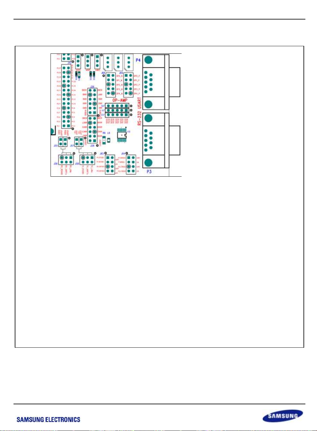
1. P3,P4: 9pin D-sub connector (Female)
2. U12: 2Channel RS-232 Transceiver (SP3232EEY)
3. J55,J56,J57,J58: Select the input signal to each block
J55: Jumper Setting (USART RX)
1-3 closed: Connect P0.0(USART_RXD0) to J56
2-4 closed: Connect P0.21(USART_RXD1) to J56
J57: Jumper Setting (USART TX)
1-3 closed: Connect P0.1(USART_TXD0) to J58
2-4 closed: Connect P0.22(USART_TXD1) to J58
J56: Jumper Setting (RX - LIN / USART / RS-485)
Connect RXD0 or RXD1 to each block (Depending on the J55 Setting)
1-2 closed: LIN RX line (LIN driver 0 / J59 terminal block)
3-4 closed: USART RX line (Transceiver ch1 / P4 D-sub)
5-6 closed: RS-485 RX line (J62 terminal block)
J56: Jumper Setting (TX - LIN / USART / RS-485)
Connect TXD0 or TXD1 to each block (Depending on the J57 Setting)
1-2 closed: LIN0 TX line (LIN driver 0 / J59 terminal block)
3-4 closed: USART TX line (Transceiver ch1 / P4 D-sub)
5-6 closed: RS-485 TX line (J62 terminal block)
2.2.5.2 Block Description
2-9
Page 20
S3FM02G_USER'S GUIDE_REV 1.00 2 EVB DESCRIPTION
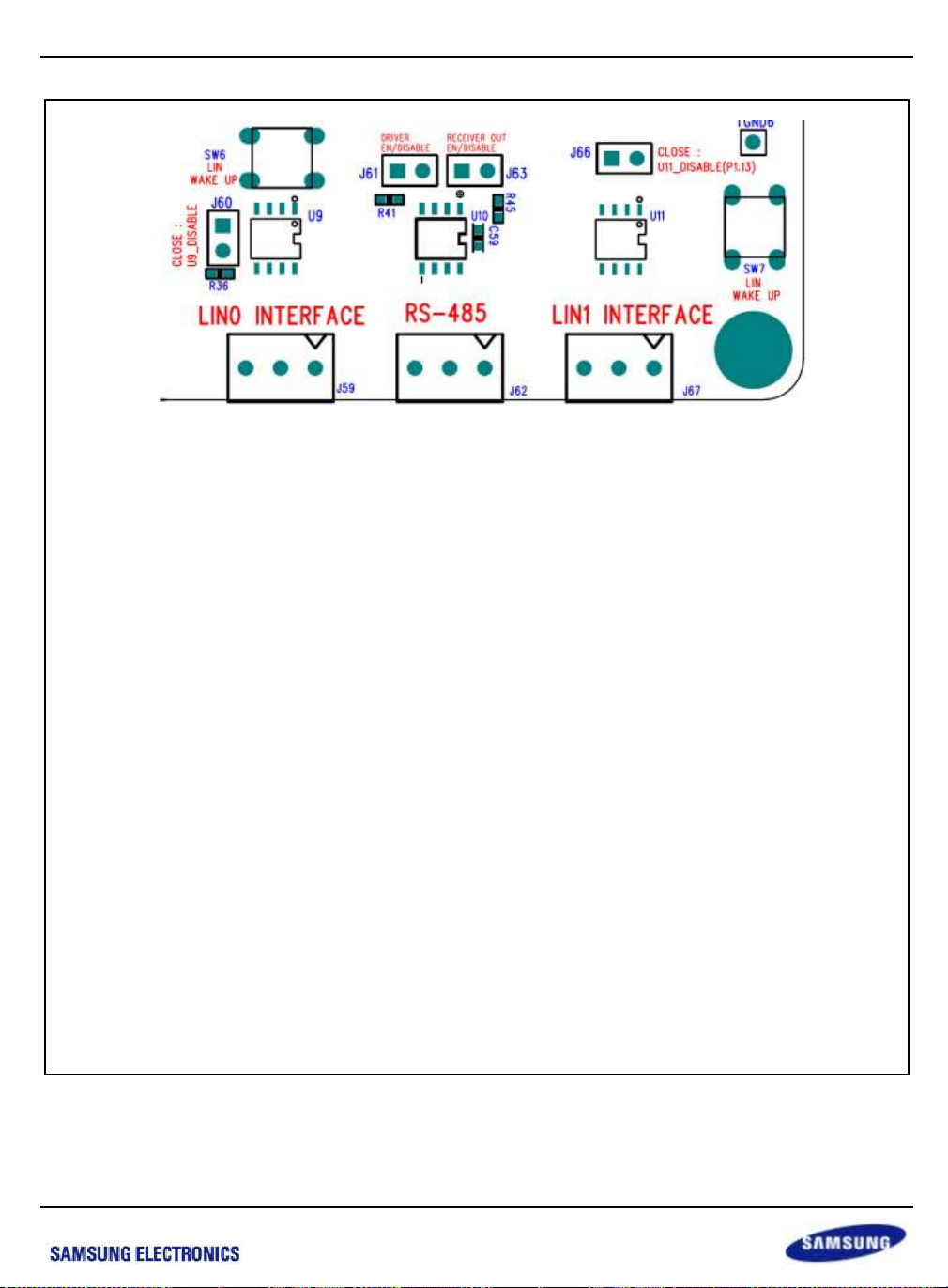
4. J64,J65: Select the input signal to USART & LIN
J64: Jumper Setting (RX - USART / LIN)
1-2 closed: Connect P1.30(USART_RXD0) to RS232 transceiver channel 0 (P3 D-sub)
3-4 closed: Connect P1.9(USART_RXD2) to LIN driver 1 (J67 terminal block)
5-6 closed: Connect P0.27(USART_RXD3) to RS232 transceiver channel 0 (P3 D-sub)
7-8 closed: Connect P0.27(USART_RXD3) to LIN driver 1 (J67 terminal block)
J64: Jumper Setting (RX - USART / LIN)
1-2 closed: Connect P1.31(USART_TXD0) to RS232 transceiver channel 0 (P3 D-sub)
3-4 closed: Connect P1.10(USART_TXD2) to LIN driver 1 (J67 terminal block)
5-6 closed: Connect P0.28(USART_TXD3) to RS232 transceiver channel 0 (P3 D-sub)
7-8 closed: Connect P0.28(USART_TXD3) to LIN driver 1 (J67 terminal block)
5. J59,J62,J67: CCP3.5 - 3pin Terminal Block
J59: LIN0 Interface / J62: RS - 485 Interface / J67: LIN1 Interface
6. U59,U62: LIN(ISO9141) Driver - TLE7259-2GU
7. U59,U62: RS-485 Transceiver - SN65HVD08
8. SW6: LIN0 Wake up
9. SW7: LIN1 Wake up
10. J60,J66: Enable input - device set to normal operation mode when HIGH
J60 closed: EN pin low state
J61 closed: EN pin port control [ P1.13 ]
11. J61: Closed - Driver EN port control [ P1.11] / Open - High state
12. J63: Closed - Receiver Out port control [ P1.12] / Open - Low state
Figure 2-6 USART Block Description
2-10
Page 21
S3FM02G_USER'S GUIDE_REV 1.00 2 EVB DESCRIPTION
2.2.6 SSP Block
2.2.6.1 Features
Up to 2 channels
Programmable data frame from 4 to 16-bit
Support Master and Slave Mode
Programmable Clock Pre-scale
Separate 16 32-bit width Transmit/Receive FIFO
Dedicated DMA channel
2-11
Page 22
S3FM02G_USER'S GUIDE_REV 1.00 2 EVB DESCRIPTION
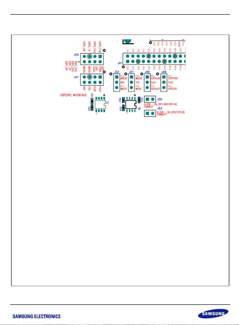
1-2 closed: Connect P0.8[ FSS 0 ] to U7[ EEPROM ] chip select pin
3-4 closed: Connect P0.9[ CLK 0 ] to U7[ EEPROM ] SSP clock pin
1. U7: EEPROM - SSP8(8Kbytes x 8-bit)
3. J47: Jumper Setting
5-6 closed: Connect P0.11[ MOSI 0 ] to U7[ EEPROM ] serial input pin
7-8 closed: Connect P0.10[ MISO0 ] to U7[ EEPROM ] serial output pin
4. 48,J49,J51,J52: Jumper Setting
2. U8: EEPROM - SSP16(4Kbytes x 16-bit)
J48: U8 [chip select] pin
1-2 closed: P1.7 / SSPFSS 0
2-3 closed: P1.3 / SSPFSS 1
J49: U8 [SSP clock] pin
1-2 closed: P1.6 / SSPCLK 0
2-3 closed: P1.2 / SSPCLK 1
J51: U8 [Serial data input] pin
1-2 closed: P1.4 / SSPMOSI 0
2-3 closed: P1.0 / SSPMOSI 1
J52: U8 [Serial data output] pin
1-2 closed: P1.5 / SSPMISO 0
2-3 closed: P1.1 / SSPMISO 1
5. J50,J53: Jumper Setting
J50 closed: U8 RDY/nBUSY pin port control [ P1.14 ]
J53 closed: U8 RESET pin port control [ P1.8 ]
6. J54: SSP Signal spare ports
2.2.6.2 Block Description
2-12
Page 23
S3FM02G_USER'S GUIDE_REV 1.00 2 EVB DESCRIPTION
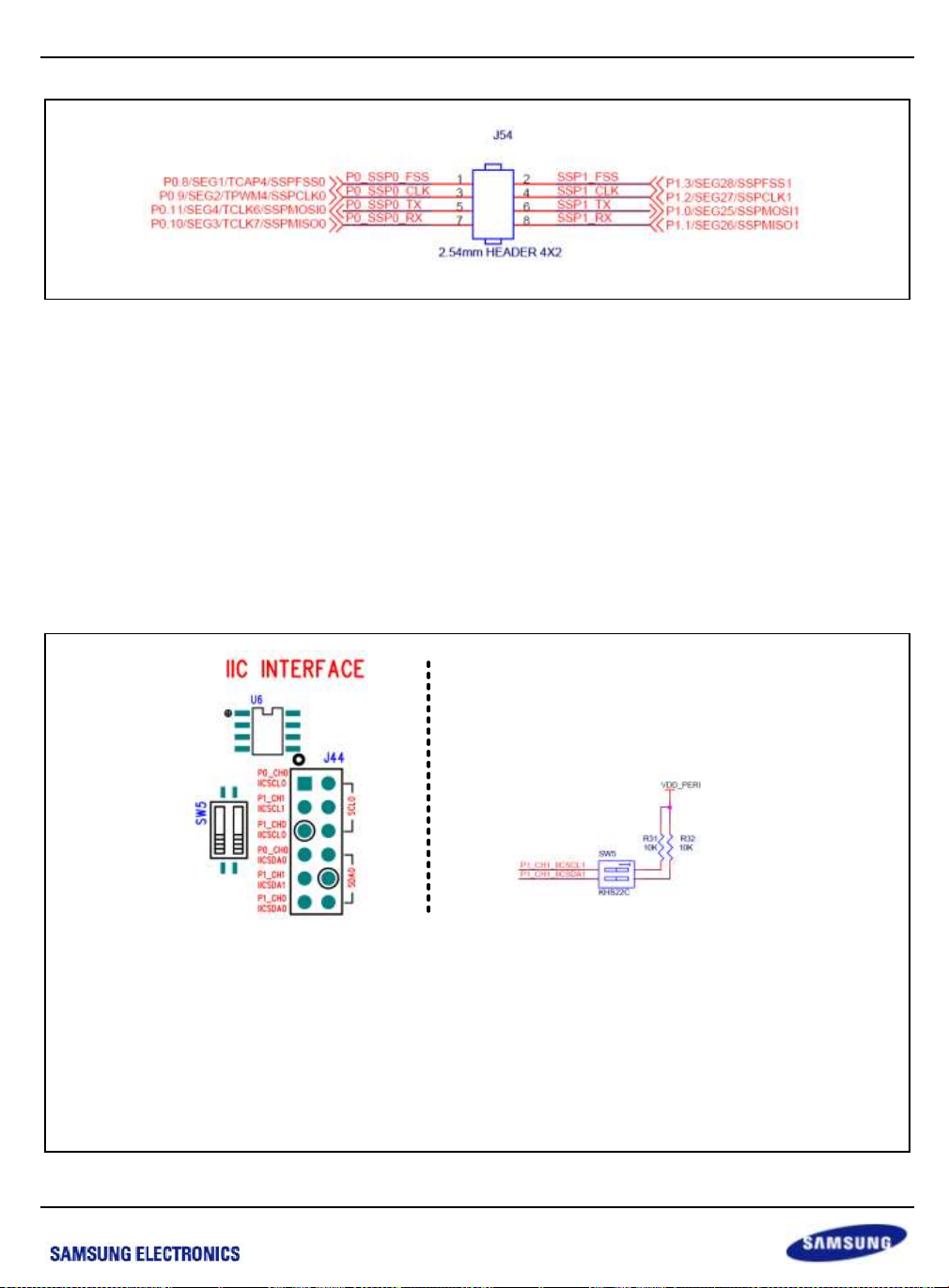
1-2 closed: Connect P0.14 [P0 CH0 IICSCL0] to U6 SCL
3-4 closed: Connect P1. 4 [P1 CH1 IICSCL1] to U6 SCL
1. U6: EEPROM(16Kbytes x 8-bit)
2. J44: Jumper Setting
5-6 closed: Connect P1.26 [P1 CH0 IICSCL0] to U6 SCL
7-8 closed: Connect P0.15 [P0 CH0 IICSDA0] to U6 SDA
9-10 closed: Connect P1.5 [P0 CH0 IICSDA0] to U6 SDA
11-12 closed: Connect P1.25 [P0 CH0 IICSDA0] to U6 SDA
3. SW5: Loopback Test
Figure 2-7 SSP Block Description
2.2.7 I2C Block
2.2.7.1 Features
Up to 2 channels
Multi-Master IIC-Bus
Serial, 8-bit Oriented and Bi-directional Data Transfers
100Kbit/s in Standard Mode and up to 400Kbit/s in Fast mode
Dedicated DMA channel
2.2.7.2 Block Description
Figure 2-8 I2C Block Description
2-13
Page 24
S3FM02G_USER'S GUIDE_REV 1.00 2 EVB DESCRIPTION
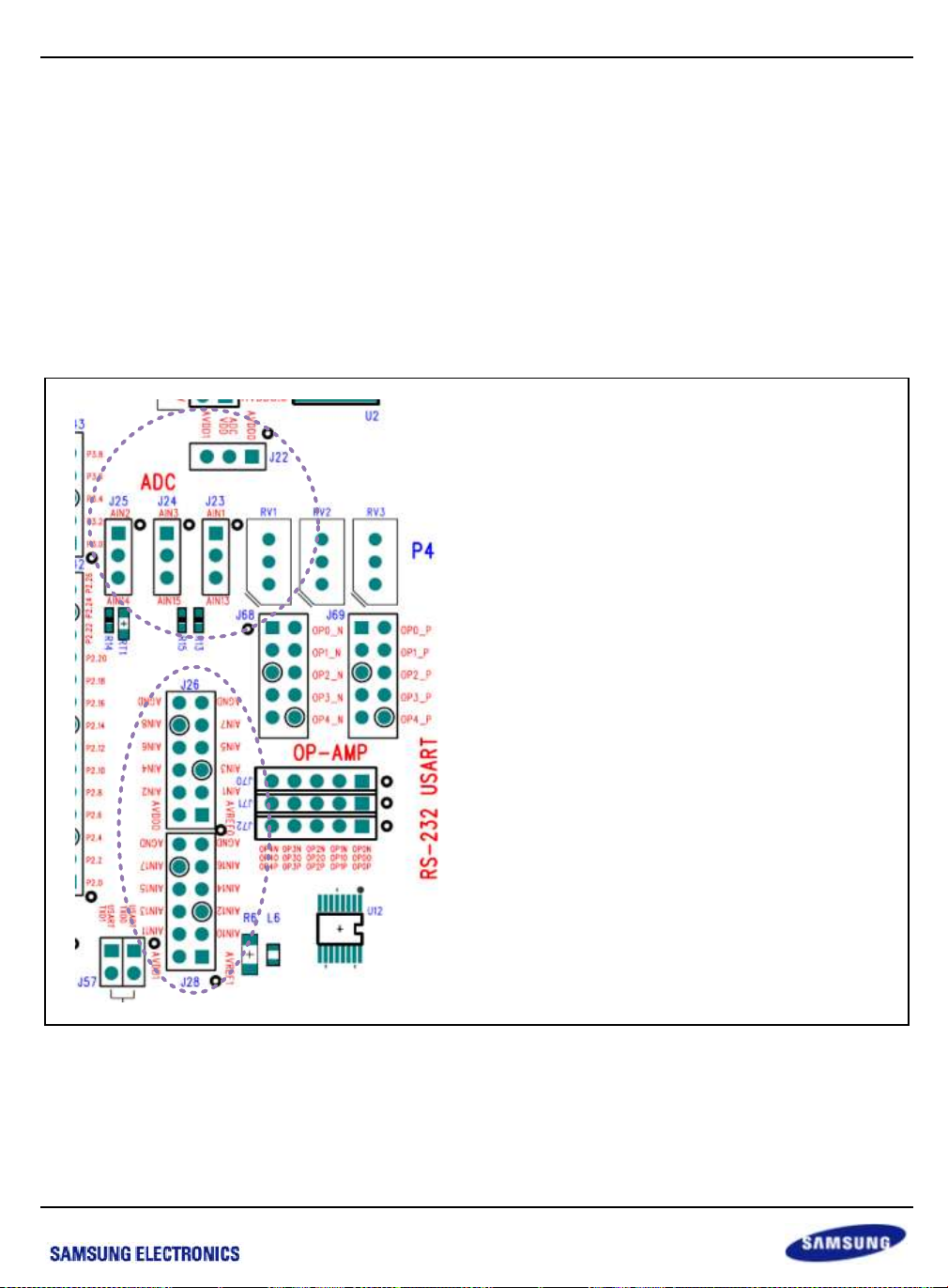
1-2 closed: AVDD 0
1. J22: ADC power select
2. J23: Adjust the value of the
Variable resistor control [ RV1 ]
3. J24: Using the value of Thermistor & resistor
2-3 closed: AVDD 1
1-2 closed: AIN01
2-3 closed: AIN13
1-2 closed: AIN02
2-3 closed: AIN14
4. J25: Using the value of Voltage dinider
1-2 closed: AIN03
2-3 closed: AIN15
5. J26: ADC spare pin - AIN01 ~ AIN08
6. J28: ADC spare pin - AIN10 ~ AIN17
2.2.8 ADC Block
2.2.8.1 Features
Up to 16 channel’s Analog Inputs
12-bit ADC0 and 10-bit ADC1
2 Op-amp for 12-bit ADC input level amplification
Supports simultaneous sampling and conversion up to 2-input channels
Dedicated DMA channel
2.2.8.2 Block Description
Figure 2-9 ADC Block Description
2-14
Page 25
S3FM02G_USER'S GUIDE_REV 1.00 2 EVB DESCRIPTION
Pin Name
Function
I/O Type
Comments
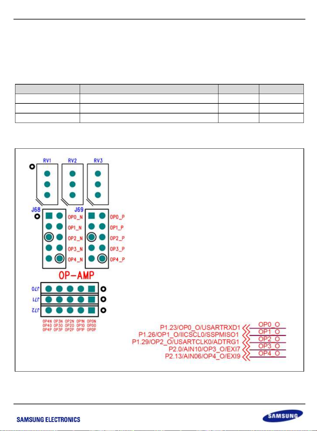
OPA_O[4:0]
Operational Amplifier Output Pin
O
–
OPA_P[4:0]
Operational Amplifier Positive input pin
I
–
OPA_N[4:0]
Operational Amplifier Negative input pin
I
–
1-2 closed: OP0_N(P1.24)
1. J68: Jumper Setting(Connected to RV2)
3. J70,J71,J72: Spare ports
7-8 closed: OP3_N(P2.1)
1-2 closed: OP0_P(P1.25)
3-4 closed: OP1_P(P1.28)
J71: OP0 ~ 4_O
J72: OP0 ~ 4_P
3-4 closed: OP1_N(P1.27)
5-6 closed: OP2_N(P1.30)
9-10 closed: OP4_N(P2.14)
R51: P2.11/AIN04 connected to RV2
2. J69: Jumper Setting(Connected to RV3)
5-6 closed: OP2_P(P1.31)
7-8 closed: OP3_P(P2.2)
R52: P2.12/AIN05 connected to RV3
J70: OP0 ~ 4_N
9-10 closed: OP4_P(P2.15)
2.2.9 OP-AMP Block
2.2.9.1 Features
Configurable internal gain from 2.5 to 10
Gain can be controlled by an external circuit
2.2.9.2 Block Description
Figure 2-10 OP-AMP Block Description
2-15
Page 26
S3FM02G_USER'S GUIDE_REV 1.00 2 EVB DESCRIPTION
2.2.10 LCD Block
2.2.10.1 Features
Four common output pins COM [3:0]
Forty segment output pins SEG [39:0]
LCD bias by internal or external resistor
Supports bias and duty mode for each corresponding operation
Programmable flame clock generator
Display Memory Registers contain the data to be displayed on the LCD
2-16
Page 27
S3FM02G_USER'S GUIDE_REV 1.00 2 EVB DESCRIPTION
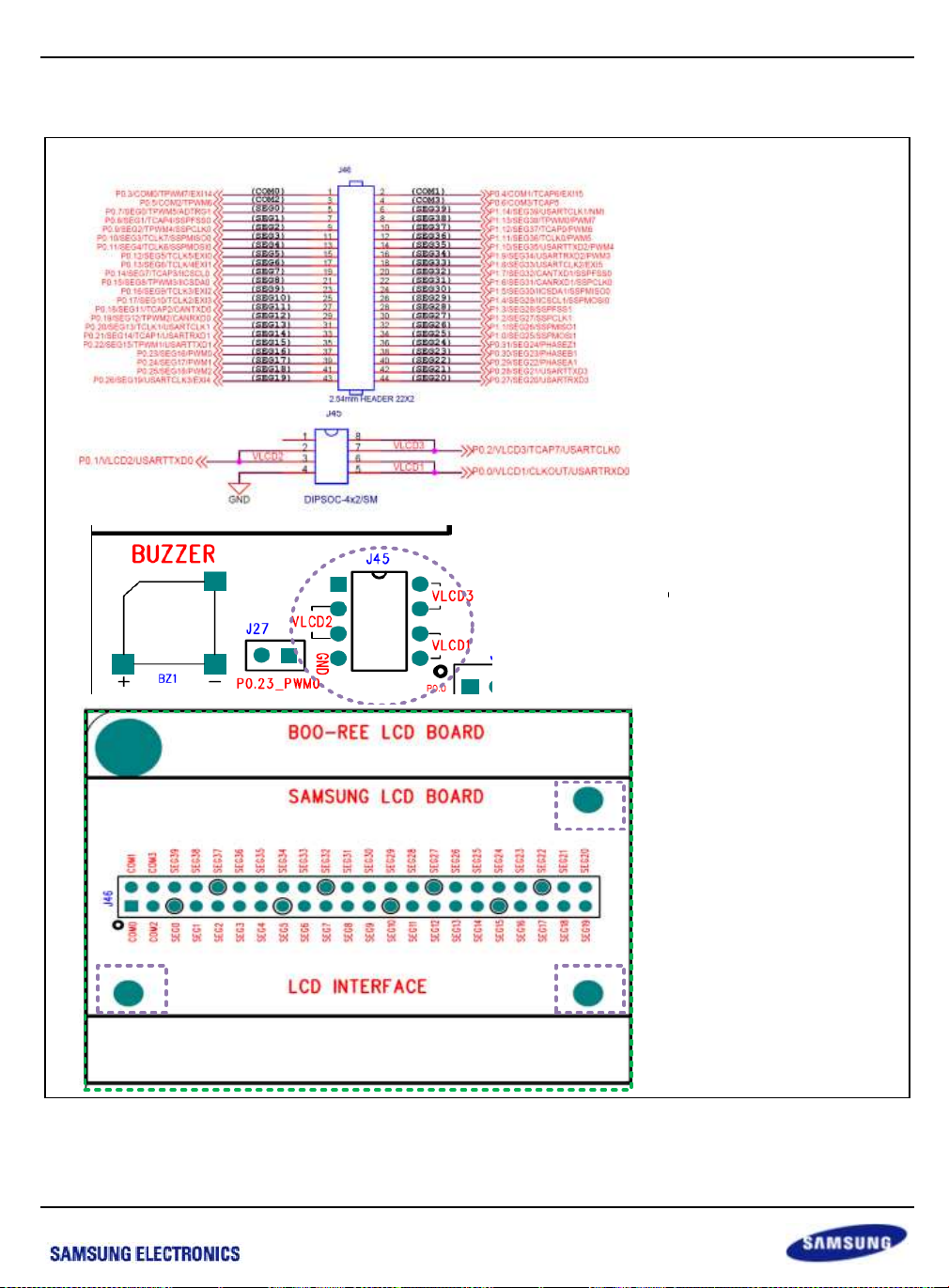
1. J45: LCD Voltage Driving
2. J46: 22x2 2.54mm Header for Side Boards
3. BOO-REE LCD Board: 64mm x 50mm Side Board
4. SAMSUNG LCD Board: 64mm x 32mm Side Board
5. 3 Support for hole
2.2.10.2 Block Description
Figure 2-11 LCD Block Description
2-17
Page 28
S3FM02G_USER'S GUIDE_REV 1.00 2 EVB DESCRIPTION
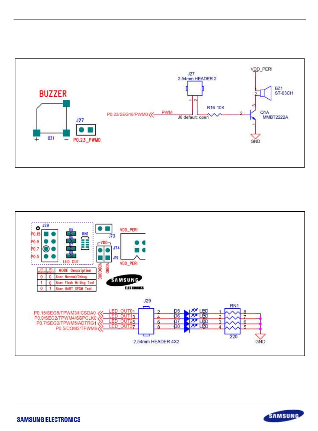
1. J27: Buzzer control (P0.23/PWM0)
1. J29: Jumper Setting (LED select)
P0.15 > D5(LED)
P0.9 > D6(LED)
P0.7 > D7(LED)
P0.5 > D8(LED)
2.2.11 Other Blocks
2.2.11.1 Buzzer
Figure 2-12 Buzzer Block Description
2.2.11.2 LED Display
Figure 2-13 LED Block Description
2-18
Page 29
S3FM02G_USER'S GUIDE_REV 1.00 2 EVB DESCRIPTION
1. J29: Jumper Setting (LED select)
2. J29: Jumper Setting (LED select)
3. J29: Jumper Setting (LED select)
4. J29: Jumper Setting (LED select)
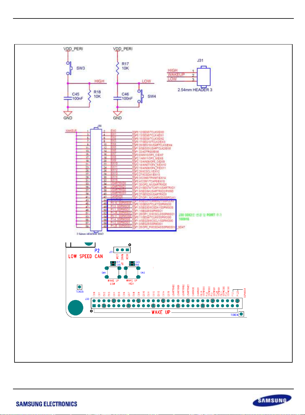
2.2.11.3 Wake Up
Figure 2-14 Wake Up Block Description
2-19
Page 30
S3FM02G_USER'S GUIDE_REV 1.00 2 EVB DESCRIPTION
Block
Symbols
Summary
Power
U2
3.3V LED
U3
5V LDO
Mode
J11
Mode 0
J13
Mode 1
CAN
U4
High speed CAN transceiver
U5
Low speed CAN transceiver
P1
9pin D-sub Male (low speed)
P2
9pin D-sub Male (high speed)
ENC
CN3
15pin D-sub Female
USART
U12
RS-232 transceiver(2CH)
P3
9pin D-sub Female(CH0)
P4
9pin D-sub Female(CH1)
LIN
U9
LIN transceiver
U11
LIN transceiver
J59
3pin 3.5mm terminal block
J67
3pin 3.5mm terminal block
RS485
U10
RS-485 transceiver
J62
3pin 3.5mm terminal block
SSP
U7
EEPROM – 8Kbytes 8-bit
U8
EEPROM – 4Kbytes 16-bit
I2C
U6
EEPROM – 16Kbytes 8-bit
ADC
J23
AIN01 or AIN13 input
J24
AIN02 or AIN14 input
J25
AIN03 or AIN15 input
OP-AMP
J68
OPA_N channel input (RV2)
J69
OPA_P channel input (RV3)
LCD
J46
Connect to side board
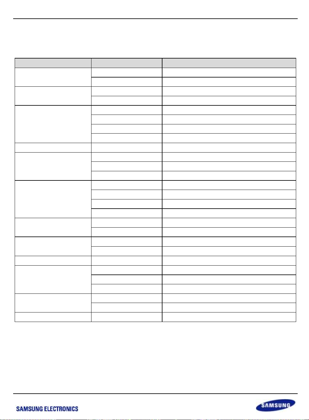
2.3 Total Blocks Unit & Jumper Summary
2.3.1 Each Blocks
2-20
Page 31
S3FM02G_USER'S GUIDE_REV 1.00 2 EVB DESCRIPTION
Parts No.
Purpose
Function Summary
SW1
Power
Power [ON / OFF]
SW2
Reset
Board reset (S3FM02G reset low)
SW3
Wake up
Wake up signal high level
SW4
Wake up
Wake up signal low level
SW5
I2C
I2C Loofback Test (3.3V input)
SW6
LIN
LIN0 Wake up (GND input)
SW7
LIN
LIN1 Wake up (GND input)
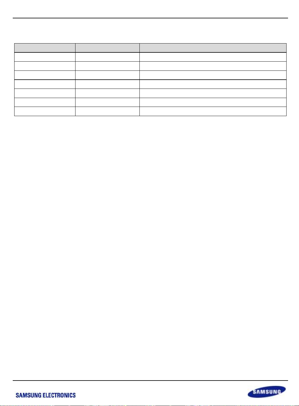
2.3.1.1 Switch
2-21
 Loading...