

Page 1
S3F84B8
All-in-One IH Cooker
Revision 0.00
May 2010
AApppplliiccaattiioonn NNoottee
2010 Samsung Electronics Co., Ltd. All rights reserved.
Page 2

Important Notice
The information in this publication has been carefully
checked and is believed to be entirely accurate at the
time of publication. Samsung assumes no
responsibility, however, for possible errors or
omissions, or for any consequences resulting from the
use of the information contained herein.
Samsung reserves the right to make changes in its
products or product specifications with the intent to
improve function or design at any time and without
notice and is not required to update this
documentation to reflect such changes.
This publication does not convey to a purchaser of
semiconductor devices described herein any license
under the patent rights of Samsung or others.
Samsung makes no warranty, representation, or
guarantee regarding the suitability of its products for
any particular purpose, nor does Samsung assume
any liability arising out of the application or use of any
product or circuit and specifically disclaims any and all
liability, including without limitation any consequential
or incidental damages.
S3F84B8 All-in-One IH Cooker
Application Note, Revision 0.00
"Typical" parameters can and do vary in different
applications. All operating parameters, including
"Typicals" must be validated for each customer
application by the customer's technical experts.
Samsung products are not designed, intended, or
authorized for use as components in systems intended
for surgical implant into the body, for other
applications intended to support or sustain life, or for
any other application in which the failure of the
Samsung product could create a situation where
personal injury or death may occur.
Should the Buyer purchase or use a Samsung product
for any such unintended or unauthorized application,
the Buyer shall indemnify and hold Samsung and its
officers, employees, subsidiaries, affiliates, and
distributors harmless against all claims, costs,
damages, expenses, and reasonable attorney fees
arising out of, either directly or indirectly, any claim of
personal injury or death that may be associated with
such unintended or unauthorized use, even if such
claim alleges that Samsung was negligent regarding
the design or manufacture of said product.
Copyright
All rights reserved. No part of this publication may be reproduced, stored in a retrieval system, or transmitted in
any form or by any means, electric or mechanical, by photocopying, recording, or otherwise, without the prior
written consent of Samsung Electronics.
Samsung Electronics Co., Ltd.
San #24 Nongseo-Dong, Giheung-Gu
Yongin-City, Gyeonggi-Do, Korea 446-711
TEL: (82)-(31)-209-3865
FAX: (82)-(31)-209-6494
Home Page:
2010 Samsung Electronics Co., Ltd.
http://www.samsungsemi.com
Page 3

Revision History
Revision No. Effective Date Description Refer to Author(s)
0.00 Mar, 2010 - Initial Draft Wei Ningning
Zhang Fan
Page 4

Table of Contents
1 OVERVIEW OF IH COOKER (IHC) .............................................................1-1
1.1 Induction Cooking Principle ..................................................................................................................... 1-1
1.1.1 How Induction Cooki
1.2 Key Features of S3F84B8........................................................................................................................ 1-2
1.3 System Princ
1.3.1 Heating
1.3.2 Protec
iple ...................................................................................................................................... 1-3
............................................................................................................................................. 1-3
tion.......................................................................................................................................... 1-3
2 HARDWARE IMPLEMENTATION...............................................................2-4
2.1 System Diagram and pi
2.2 Power Supply
2.3 Synchronization Circ
2.4 Power c
2.4.1 Voltage Meas
2.4.2 Current Measurement
2.5 System Protec
2.5.1 Surge P
2.5.2 IGBT over Voltage Protection
2.5.3 Over/under Voltage Protec
2.5.4 Temperature Protec
2.6 Other Func
2.6.1 Pan Det
2.6.2 Buzzer and Fan Control
2.6.3 Key and Display Circuit
........................................................................................................................................... 2-6
ontrol ........................................................................................................................................... 2-9
tion.................................................................................................................................. 2-11
rotection ............................................................................................................................. 2-11
tions...................................................................................................................................... 2-13
ection ................................................................................................................................. 2-13
ng Works ......................................................................................................... 1-1
n Assignment...................................................................................................... 2-4
uit ............................................................................................................................ 2-7
urement ...................................................................................................................... 2-9
..................................................................................................................... 2-10
......................................................................................................... 2-11
tion ....................................................................................................... 2-11
tion.................................................................................................................. 2-12
.................................................................................................................. 2-13
.................................................................................................................. 2-14
3 SOFTWARE IMPLEMENTATION ...............................................................3-1
3.1 State Transition Diagram
3.2 Software Diagram
3.3 Internal Resource Arrangement and
......................................................................................................................... 3-1
.................................................................................................................................... 3-2
Configuration ................................................................................. 3-4
4 APPENDIX...................................................................................................4-1
4.1 Error Code
4.2 Schmatic .................................................................................................................................................. 4-1
4.3 Source Code
................................................................................................................................................ 4-1
............................................................................................................................................ 4-1
Page 5

List of Figures
Figure Title Page
Number Number
Figure 1-1 How IH Cooker Work
Figure 1-2 Pin Assignment in S3F84B8
Figure 2-1 Block Diagram of IH Cooker Sys
Figure 2-2 Power Suppl
Figure 2-3 Power Suppl
Figure 2-4 Waveform of the Sync
Figure 2-5 Voltage Measurement and
Figure 2-6 Current Measurement Circuit
Figure 2-7 Over-Temperature Protec
Figure 2-8 Buzzer and Fan Control
Figure 2-9 Key and Display Circuit
Figure 3-1 State Trans
Figure 3-2 Software Diagram
Figure 3-3 Interrupt Servic
Figure 3-4 Fan and B
y Circuit ........................................................................................................................ 2-6
y Circuit ........................................................................................................................ 2-7
ition Diagram .................................................................................................................. 3-1
UZ Workflow..................................................................................................................... 3-3
s ...................................................................................................................... 1-1
............................................................................................................. 1-2
tem ................................................................................................ 2-4
hronization Circuit ......................................................................................... 2-8
Surge Protection Circuit ........................................................................ 2-9
.......................................................................................................... 2-10
tion ......................................................................................................... 2-12
.................................................................................................................. 2-13
................................................................................................................... 2-14
............................................................................................................................. 3-2
e Routine Diagram ................................................................................................... 3-3
Page 6

List of Tables
Table Title Page
Number Number
Table 2-1 S3F84B8 pin assignment in IH c
Table 3-1 Internal Resource Arrangement and Configuration
Table 4-1 Error Information
................................................................................................................................ 4-1
ooker system .................................................................................. 2-5
........................................................................... 3-4
Page 7
S3F84B8_ALL-IN-ONE IH COOKER_AN_REV 0.00 1 OVERVIEW OF IH COOKER (IHC)
1 OVERVIEW OF IH COOKER (IHC)
In traditional ranges or ovens, cookware is used to transfer heat from the stove elements. However, in the IH
cooker (IHC), the cookware participates in the heat generation. This form of heat generation is known as Induction
Heating, and it improves the overall thermal efficiency of heating.
This document describes an IH cooker (IHC) system implemented with Samsung’s newly developed 8-bit MCU
S3F84B8, which is designed for an all-in-one IHC application with amplifier and comparators.
1.1 INDUCTION COOKING PRINCIPLE
According to Faraday’s Law, changing the magnetic field associated with an alternating current (AC) induces
current in a second conductor placed in that field. IH cookers work largely the same way.
1.1.1 HOW INDUCTION COOKING WORKS
section describes how induction cooking works.
This
Steps:
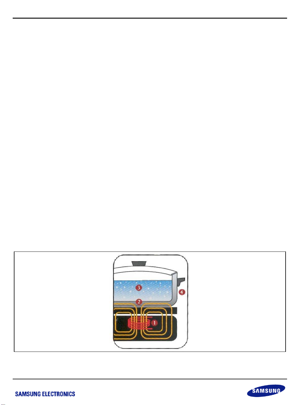
1) The electronic components in the element power a coil, which in turn produces a high-frequency
electromagnetic field.
2) The electromagnetic field enters the ferrous metal (magnetic material) of the cookware and sets up a
circulating electric current (Eddy current), which generates heat.
3) The heat generated in the cookware is transferred internally.
4) The electromagnetic field does not affect the outer body of cookware. As soon as the cookware is removed
from the element or the element turned off, the heat generation stops.
Figure 1-1 How IH Cooker Works
1-1
Page 8
S3F84B8_ALL-IN-ONE IH COOKER_AN_REV 0.00 1 OVERVIEW OF IH COOKER (IHC)
1.2 KEY FEATURES OF S3F84B8
With no more discrete ICs like LM339 (comparator IC) in previous IHC solutions, S3F84B8 successfully integrates
four comparators, one OPA, and one IH-PWM to control power directly. After configuration, all the four
comparators can cooperate with the IH-PWM automatically, which makes the time-sensitive control possible.
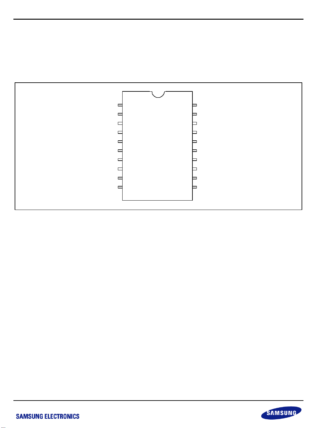
Figure2 shows the pin assignment in S3F84B8.
V
INT0/XIN/P0.0
INT1/X
OUT
/P0.1
V
PP
/nRESET/P0. 2
BUZ/INT2/P0.3
PWM/INT3/P0.4
INT4/P0.5
TAOUT/INT5/P0.6
TACK/CMP0_P/P1.0
TACAP/CMP0_N/P1.1
1
SS
2
3
4
5
6
7
8
9
10
S3F84B8
20-DIP/
20-SOP
V
20
DD
P2.7/ADC7/(SCL)
19
P2.6/ADC6/(SDA)
18
P2.5/ADC5/CMP3_N
17
P2.4/ADC4/CMP2_N
16
P2.3/ADC3(OPA_O)
15
P2.2/ADC2/OPA_N
14
P2.1/ADC1/OPA_P
13
P2.0/ADC0/TDOUT
12
P1.2/CMP1_N
11
Figure 1-2 Pin Assignment in S3F84B8
The key features of S3F84B8 include:
8K Full Flash ROM and 272B SRAM
Four Comparators
One OPA
10-bit IH-PWM x 1 (can co-operate with the four Comparators)
10-bit ADC x 8
8-bit Basic Timer (can be used as Watch Dog Timer)
8-bit TimerA
16-bit Timer0 (can be used as two 8-bit Timers C/D)
External Interrupts X 6
Supports configurable LVR (1.9/2.3/3.6/3.9V)
Supports configurable internal RC (0.5M/8MHz RC @5V with maximum 3% accuracy)
Supports 18 IOs (maximum) when using internal LVR and internal RC
Comparator0 has two inputs. Its output can trigger the PWM to start a new cycle immediately or after some
programmable delay. This helps in the synchronization control. The delay can adjust the IGBT to turn on at
minimum collector voltage, thereby reducing the heat and protecting the transistor.
1-2
Page 9

S3F84B8_ALL-IN-ONE IH COOKER_AN_REV 0.00 1 OVERVIEW OF IH COOKER (IHC)
Comparator1/2/3 has only one input with an internal programmable reference level. It can lock the output of PWM
to a safe level. Besides the delay trigger function, PWM can realize anti-mis-trigger function as well. It prevents
the PWM from being triggered by unexpected noise. For more information about the cooperating mechanism of
the IH-PWM and four comparators, refer to the user’s manual.
1.3 SYSTEM PRINCIPLE
To make the system work reliably, the control of IH cooker can be divided into two major parts: heating and
protection.
1.3.1 HEATING
In earlie
r solutions, the output of LM339 controls the IGBT. On being filtered, the PWM output transforms into an
analog signal that sets the flip level of LM339. Therefore, only the duty determines the output power.
However, in a system with S3F84B8, the PWM directly controls the switch of IGBT and the width of valid output
level determines the output power. Therefore, the power is dependent on the system clock.
1.3.2 PROTECTION
kinds of protection are available for the control of IH cooker: first is time sensitive protection, and the other is
Two
acceptable protection that can be executed even after certain degree of delay.
Surge protection and IGBT over-voltage protection belong to the former class (time sensitive protection).
Therefore, these two signals use the integrated comparators. In this solution, PWM will be hard-locked when
surge protection is triggered. It stops the PWM with a safe output level until the software enables it again. Once
the voltage sensed at IGBT is beyond limitation, PWM will be soft-locked. This will make the PWM stop the current
cycle and reload PWMDATA with a preset safe value (PWMPDATA) to reduce the turn-on time of IGBT from that
instance.
Over-temperature, over-current, and over/under voltage protections belong to the latter class. They are realized by
AD conversion and software comparison.
1-3
Page 10
S3F84B8_ALL-IN-ONE IH COOKER_AN_REV 0.00 2 HARDWARE IMPLEMENTATION
2 HARDWARE IMPLEMENTATION
2.1 SYSTEM DIAGRAM AND PIN ASSIGNMENT
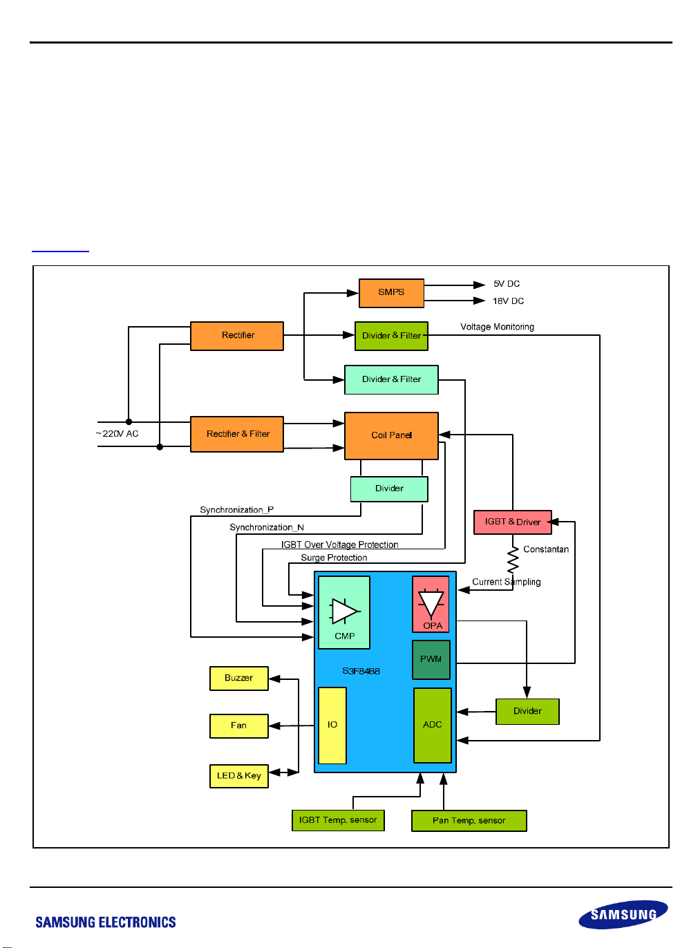
Figure 2-1 shows the block diagram of IH cooker system.
Figure 2-1 Block Diagram of IH Cooker System
2-4
Page 11
S3F84B8_ALL-IN-ONE IH COOKER_AN_REV 0.00 2 HARDWARE IMPLEMENTATION
In Figure 2-1, SMPS stands for Switch Mode Power Supply. It provides +18V DC and +5V DC to the system.
Three out of four comparators are used in this solution: one for synchronization circuit and other two for surge
protection and IGBT over-voltage protection.
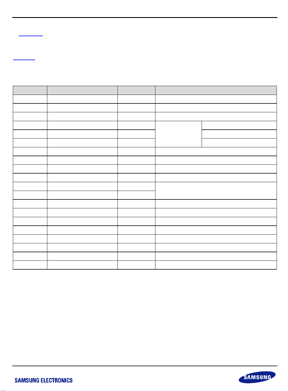
Table 2-1
shows the pin assignment while using S3F84B8 in IH cooker system.
Table 2-1 S3F84B8 pin assignment in IH cooker system
Pin No. Pin Names Pin Type Pin Assignment
1 VSS I Ground
20 VDD I Power input
4 P0.2 - Reserved
2 P0.0 O DIO
3 P0.1 O CLK
Display Board
Connector
7 P0.5 O
8 P0.6 O Reserved
13 P2.1 O Reserved
5 P0.3/BUZ O Buzzer and Fan control
6 P0.4/PWM O IGBT control
9 P1.0/CMP0_P I
Synchronization control
10 P1.1/CMP0_N I
11 P1.2/CMP1_N I IGBT over-voltage protection
16 P2.4/CMP2_N I Surge protection
17 P2.5/ADC5 I System voltage measurement input
12 P2.0/ADC0 I IGBT temperature sensor input
19 P2.7/ADC7 I Pan temperature sensor input
18 P2.6/ADC6 I Amplified current signal input
14 P2.2/OPA_N I System current measurement input
15 P2.3/OPA_O O Operational Amplifier output
STB
2-5
Page 12
S3F84B8_ALL-IN-ONE IH COOKER_AN_REV 0.00 2 HARDWARE IMPLEMENTATION
2.2 POWER SUPPLY
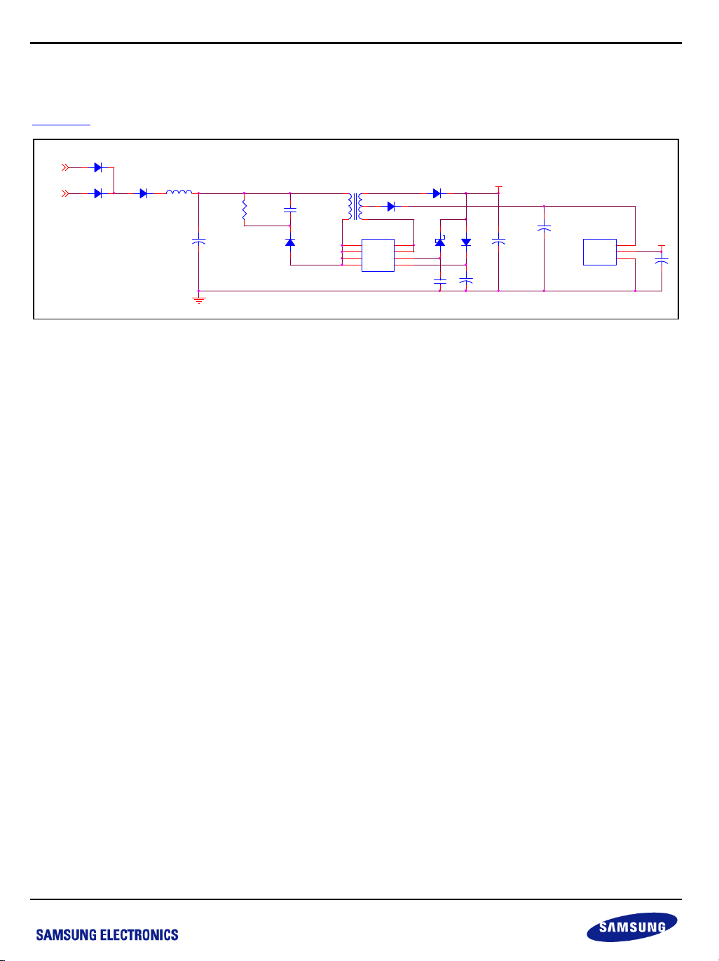
Figure 2-2 shows the circuit diagram for power supply.
AC_L
220 VAC
AC_N
D6
D7
1N4007
1N4007
D1
1N4007
L1
330uH
C2
+
4.7uF/450V
R1
100K/0.5W
C1
102/1KV
D2
UF4007
T1
1 5
4 8
EE-19
8
7
6
5
6
U1
D4
D3
D2
D1
VDD
VIPER12A
D7 UF4007
1
S1
2
S2
3
FB
4
D4 UF4007
Z1
18V
C3
104
UF4007
D5
+
C8
10uF/50V
+18V
C21
+
100uF/25V
+
C6
100uF/25V
78L05
IC1
VOUT
GND
1
VIN
3
2
Figure 2-2 Power Supply Circuit
The power circuit contains a transformer, an SMPS primary switcher, and a +5V DC regulator. After passing
through a half-wave rectifier and an LC filter, the 220V AC power enters the primary side of transformer.
Thereafter, VIPER12 and 78L05 produce stable +18V DC power for the transistors and +5V DC power for the
MCU and other devices.
+5V
+
C13
100uF/16V
2-6
Page 13
S3F84B8_ALL-IN-ONE IH COOKER_AN_REV 0.00 2 HARDWARE IMPLEMENTATION
2.3 SYNCHRONIZATION CIRCUIT
+18V
R28 51R
+
C28
25V/100uF
R23 2K
C23 102
PWM
R24
1K
IGBT Driver
AC_L
AC_N
FUSE1
10A/250V
C22
0.1uF/275V
1
-+
2
BRID GE
D15XB80H18
3
Q1
8050
R21
2K
Q2
8050
R22
2K
D8
Q4
4148
8050
R36
8550
10R
Q5
R37
10K
C17
101
C19
4uF/400V
R3
470K/0.5W
R10
470K/0.5W
R11
5K6
COOKER
L3
C20
0.24uF/1200V
IGBT
FGA15N120
R50
CONSTANTAN
R2
220K/0.5W
R6
220K/0.5W
R7
220K/0.5W
R8
220K/0.5W
Syn_P
R25
24K
R9
2KJ
IGBT_V_P
IGBT over voltage protection
R12
2K7
IGBT_CTRL
SYS_I
L2
CHOKE
4
Syn_N
Figure 2-3 Power Supply Circuit
2-7
Page 14
S3F84B8_ALL-IN-ONE IH COOKER_AN_REV 0.00 2 HARDWARE IMPLEMENTATION
IH heating is the result of Eddy current caused by LC resonance. For a general cookware, the oscillation
frequency may vary from 20KHz to 30KHz. Since heating consumes energy, the IGBT should be periodically
turned on to allow the 220V power to compensate for the energy loss. Obviously, the longer it is turned on, the
more energy can be accumulated.
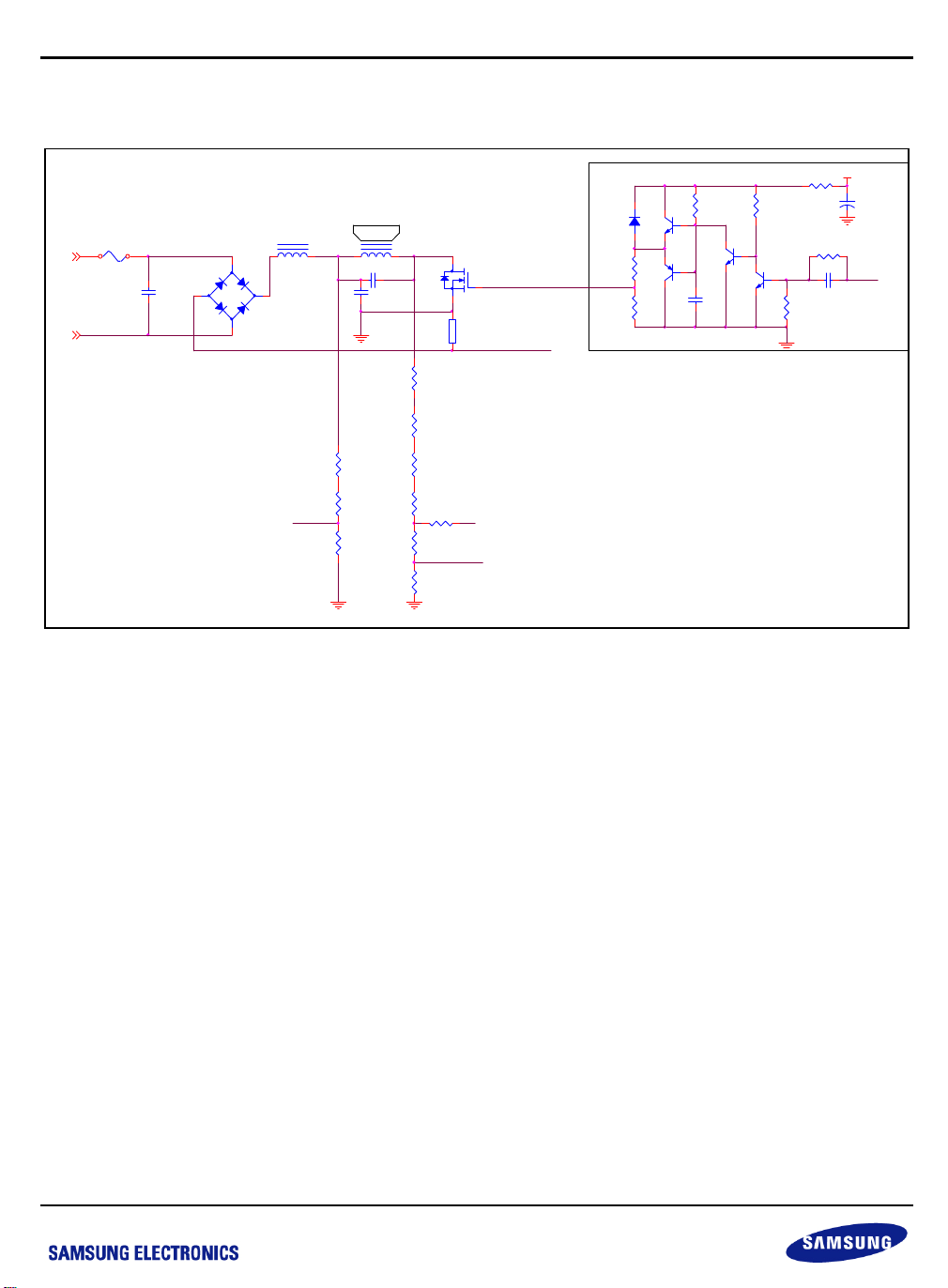
When the PWM output turns on the IGBT, electric energy is stored in the inductance and free LC oscillation is
started when the IGBT is turned off (as shown in Figure 2-3).
To make the system
work stably, consider the turn on frequency and turn on time of the IGBT. First, the turn on
frequency cannot destroy the LC oscillation, even though the IGBT on time will affect it a little bit. This means the
frequency of PWM output should be synchronized with the LC oscillation. It is realized by comparator0.
Second, considering the withstand voltage of IGBT, it is better to turn it on when the collector voltage is near ‘0’. It
can be realized by adjusting the divider resistors and enabling the delay trigger function of the IH PWM module. At
the same time, when proper delay time is set, thermal radiations will be largely reduced.
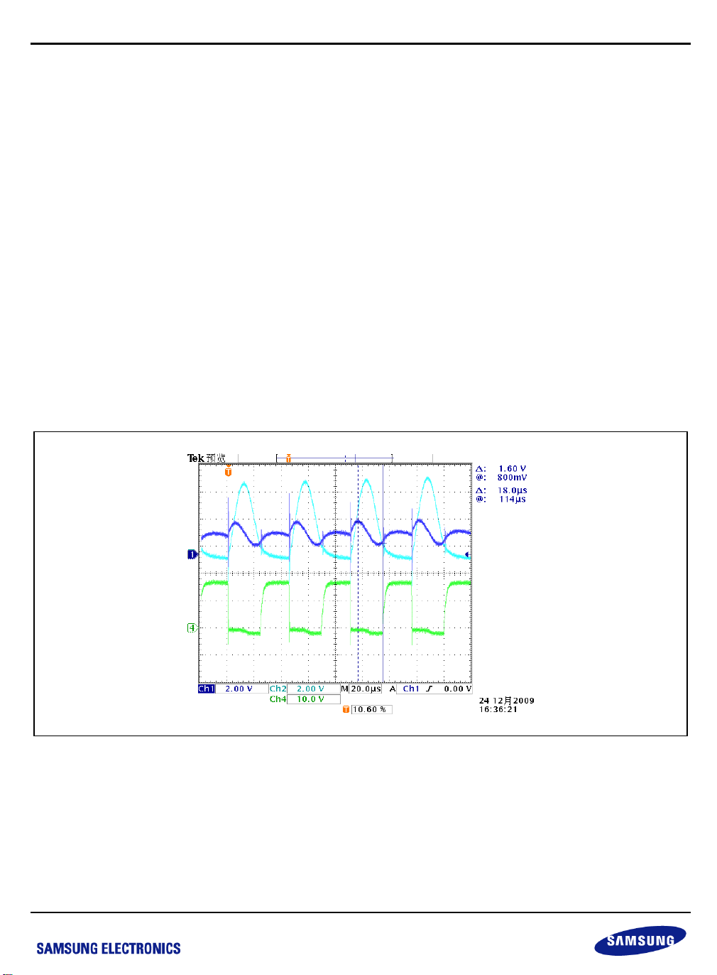
Figure6 shows the waveform of synchronization circuit. Light and dark blue waveforms show the inputs of
comparator0. The green waveform is measured at P0.4 (PWM). Additionally, the crossing point of the light and
dark blue waveforms trigger the rising of PWM output (High level at the base) which turns on the IGBT. The
duration of PWM’s outputting high is the result of software power control. When PWM output (green waveform)
returns to low level, the light and dark waveform presents free oscillation of the circuit, though the existence of the
IGBT diode makes the oscillation waveform not an ideal one.
Figure 2-4 Waveform of the Synchronization Circuit
2-8
Page 15
S3F84B8_ALL-IN-ONE IH COOKER_AN_REV 0.00 2 HARDWARE IMPLEMENTATION
2.4 POWER CONTROL
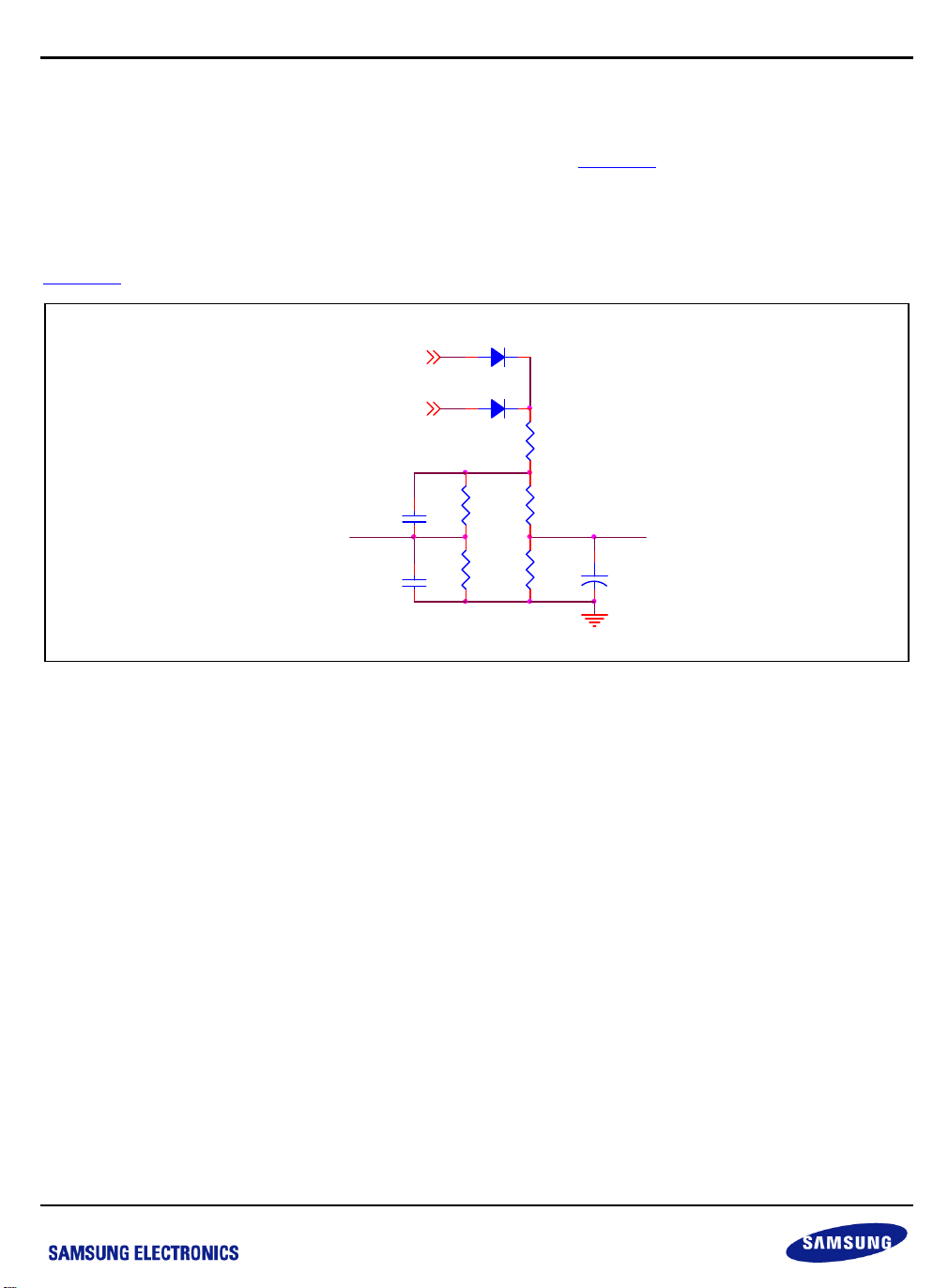
Power is the product of voltage and current (P = V x I). Figure 2-5 and
system voltage and current, separately.
2.4.1 VOLTAGE MEASUREMENT
Figure 2-5
shows the circuit diagram for voltage measurement and surge protection.
1N4007
AC_L
D9
220 VAC
C15
102/1KV
C18
221
D10
1N4007
R18
820K/0.5W
R27
6K8
R17
470K/0.5W
R19
820K/0.5W
R20
29K
AC_N
surge protection
Surge_P
Figure 2-5 Voltage Measurement and Surge Protection Circuit
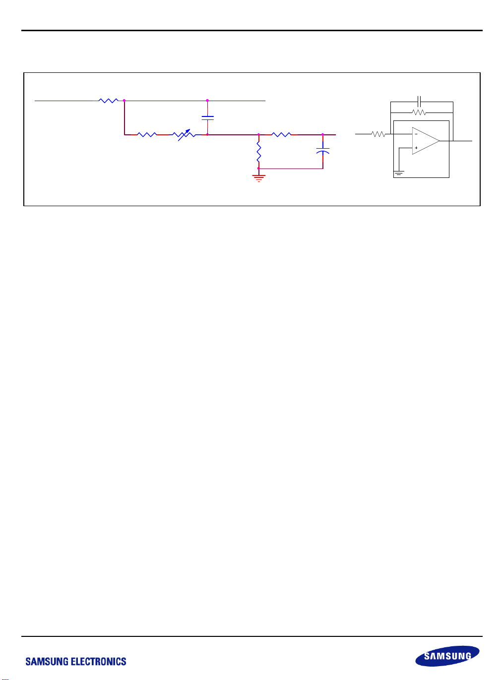
Figure 2-6 show the measurement circuit of
SYS_V
C16
+
10uF/50V
Resistor divider decreases the voltage level to the proper ADC range.
2-9
Page 16
S3F84B8_ALL-IN-ONE IH COOKER_AN_REV 0.00 2 HARDWARE IMPLEMENTATION
f
A
_
A
_
f
/
2.4.2 CURRENT MEASUREMENT
C10
104J
OPA_N
OPA_O
R14 100K
R15
22K
CURRENT
+
C12
1uF/16V
R 1
OPA
_ N
OP
P
S3F84B8
= -
R
Gain
R
OP
O
R1
SYS_I
R4 1K
R13 36K
RW1
10K
Figure 2-6 Current Measurement Circuit
In the IH cooker system, the current can go as high as 10A. To avoid excessive energy loss, a constantan is used
to change the current signal to voltage signal, which is then amplified by the integrated OPA. Finally, the amplified
signal enters the ADC module. Note that the signal (OPA_N) reaching OPA is negative as compared to MCU
GND. Therefore, OPA has to work as an inverting amplifier with negative gain.
Either the OPA offset or the resistance deviation can lead to inconsistency of output power among different chips.
To get precise power control, two calibrating methods are used. In hardware, a variable resistor (RW1) is chosen,
whereas in software algorithm, the overall offset is measured and calculated before the system starts working. It
likes the quiescent bias that should be removed during normal operation. This way the output power can be
controlled within 10W deviation.
2-10
Page 17

S3F84B8_ALL-IN-ONE IH COOKER_AN_REV 0.00 2 HARDWARE IMPLEMENTATION
2.5 SYSTEM PROTECTION
2.5.1 SURGE PROTECTION
Figure 2-5
shows the circuit diagram for surge protection. In this figure, Surge_P specifies the negative input of
Comparator 1. Also, reference voltage is internally set as 0.55VDD. When surge takes place, that is, V Surge_P >
0.55VDD, the falling edge of comparator 1 can hard-lock the PWM output immediately to prevent the IGBT from
being burnt out by over current. The whole system then stops work and restarts after some delay.
2.5.2 IGBT OVER VOLTAGE PROTECTION
IGBT over voltage is mo
Figure 2-5
shows the voltage measurement circuit. In this figure, IGBT_V_P specifies the negative input of
st likely to occur the moment when the pan is removed from the panel.
Comparator 2. Also, reference voltage internally is set as 0.70VDD. When V Surge_P > 0.70VDD, the cooperation of comparator 2 and IH PWM will soft-lock the PWM output immediately to prevent the IGBT from being
burnt out by over stress of the collector voltage. As a result, it makes the PWM stop the current cycle and reload
PWMDATA with a preset safe value (PWMPDATA) to reduce the turn-on time of IGBT.
2.5.3 OVER/UNDER VOLTAGE PROTECTION
Over/und
er voltage protection uses the voltage measurement signal. The protection takes place when the AD
conversion result is either too large or too small. The whole system then stops working until the power returns to
normal.
2-11
Page 18
S3F84B8_ALL-IN-ONE IH COOKER_AN_REV 0.00 2 HARDWARE IMPLEMENTATION
2.5.4 TEMPERATURE PROTECTION
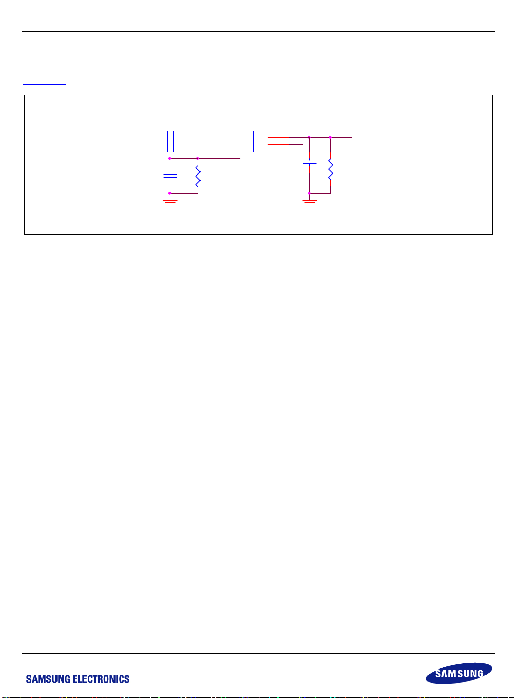
Figure 2-7
shows the circuit diagram for temperature protection.
+5V
CN5
RT1
100K3950
C4
104
R5
10K
IGBT_T
T_PAN
2
1
a) Pan temperature protectionb) IGBT temperature protection
+5V
PAN_T
C25
104
R29
3K
Figure 2-7 Over-Temperature Protection
RT1 is a thermistor located just beneath the IGBT. CN5 is the connector for the thermistor near the pan.
For IGBT temperature protection, there are two kinds of scenarios:
When the temperature rises above 85℃, the set level of output power will automatically downgrade.
When the temperature continues to rise above 90℃, the system will shut down and will remain in that state
until it is restarted manually.
For pan temperature, the system will be shut down when the temperature is over 230℃.
The threshold of protection level can differ, according to the different locations of the thermistor.
Meantime, when the sensed voltage level is close to 5V or 0V, the sensor can be viewed as broken. The whole
system then stops working until it is restarted manually.
2-12
Page 19
S3F84B8_ALL-IN-ONE IH COOKER_AN_REV 0.00 2 HARDWARE IMPLEMENTATION
2.6 OTHER FUNCTIONS
2.6.1 PAN DETECTION
Pan-on detection is executed every 2sec when the system is idle. It is useful when you press the Start key first
and then put the pan on. In principle, even though the IGBT is turned on, there will not be any oscillation before
the pan is put on the panel. In S3F84B8, comparator 0’s output can be set as the clock source of Timer C. After
starting 1-cycle PWM output and waiting for about 3 oscillation cycles, if TCCNT>1, Pan status = on; else Pan
status = off. Pan-remove detection is executed every 1.5s when the system is working. It is useful when you
directly remove the pan from the panel without pressing the Stop key.
Pan-remove detection is done by current measurement, that is, when the sensed current is small, the system
considers the pan as removed and turns idle.
2.6.2 BUZZER AND FAN CONTROL
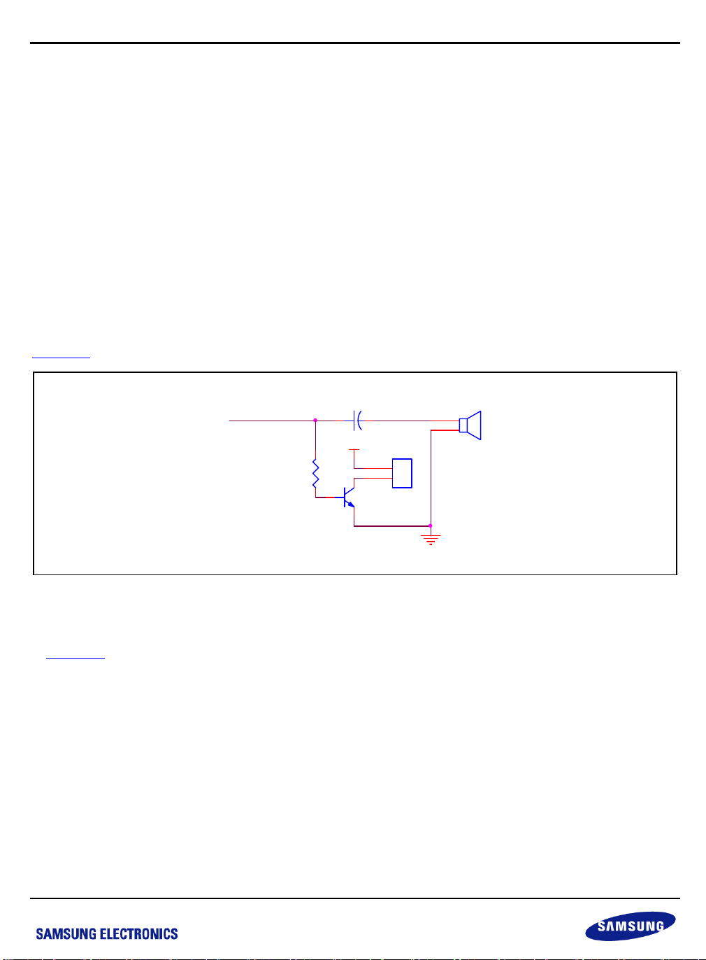
Figure 2-8
shows the circuit diagram for buzzer and fan control.
C24 104M/50V
R26
1K
+18V
+
1
2
Q3
8050
BUZ/FAN
BUZZER1
CN3
FAN
Figure 2-8 Buzzer and Fan Control
The fan cools down the system while heating. Buzzer indicates error and key actions.
In
Figure 2-8
, buzzer and fan share the same I/O. Due to C24, the DC signal controls fans on and off, while
square wave with high frequency determines the buzzer’s beep.
Note that C24 cannot be too large; else it will deteriorate the power of MCU and make the integrated analog
modules work unstably.
2-13
Page 20
S3F84B8_ALL-IN-ONE IH COOKER_AN_REV 0.00 2 HARDWARE IMPLEMENTATION
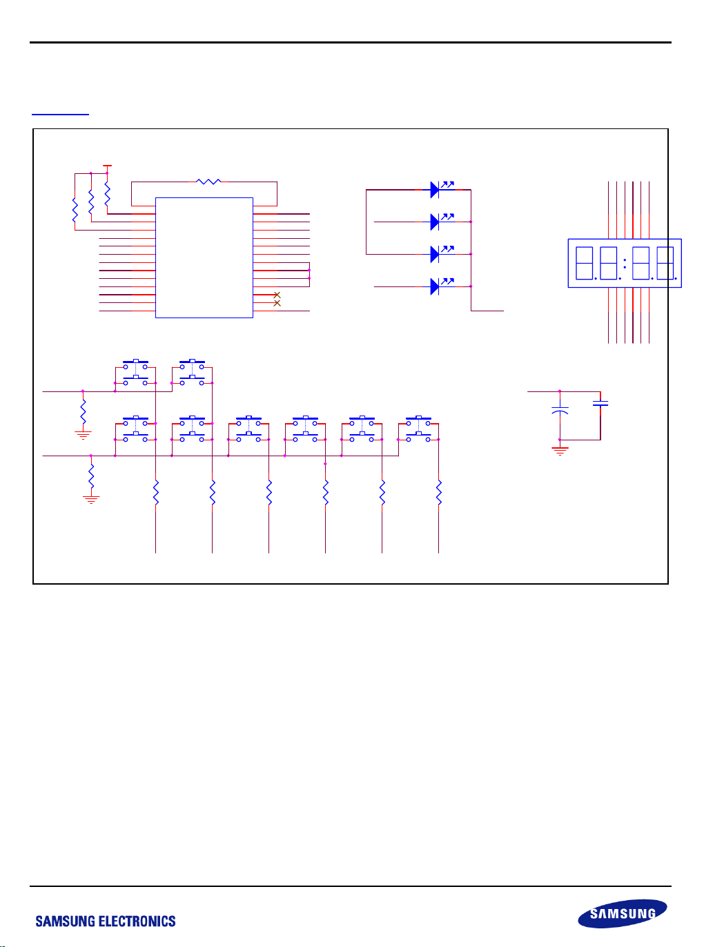
2.6.3 KEY AND DISPLAY CIRCUIT
Figure 2-9
21
cons tant
R8
const ant
cons tant
KEY1
R18 c onstant
KEY2
R17
shows the circuit diagram for key and display.
5V
R29
2 1
21
21
R32
KEY1
KEY2
5V
SEG1/KS1
SEG2/KS2
SEG3/KS3
SEG4/KS4
SEG5/KS5
SEG6/KS6
SEG7/KS7
K4 KEY K2 KEY
K3
0
KEY
constant
2 1
0
10
11
12
13
14
R9
1
2
3
4
5
6
7
8
9
2 1
U2
NC
DIO
CLK
STB
KEY1
KEY2
VDD0
SEG1/KS1
SEG2/KS2
SEG3/KS3
SEG4/KS4
SEG5/KS5
SEG6/KS6
SEG7/KS7
TM1628
K1
KEY
constant
cons tant
SEG14/GRI D5
SEG13/GRI D6
SEG12/GRI D7
SEG8/KS8
R7
2 1
21 R6
GND0
GRID 1
GRID 2
GND
GRID 3
GRID 4
GND1
VDD1
SEG10
SEG9
K5
KEY
const ant
R10
28
27
26
25
24
23
22
21
20
19
18
17
16
15
GRID 1
GRID 2
GND
GRID 3
GRID 4
GND
5V
GRID 5
GRID 6
GRID 7
SEG8/KS8
2 1
K6
KEY
const ant
R11
2 1
K7
KEY
cons tant
R12
SEG1/KS1
SEG4/KS4
SEG3/KS3
2 1
D1
1 2
LED
D2
1 2
LED
D3
1 2
LED
D4
1 2
LED
K8
KEY
cons tant
R14
2 1
GRID 7
const ant
GRID 1
GRID 2
GRID 3
SEG8/KS8
SEG6/KS6
SEG7/KS7
D8
4LED
5V
12
C26
+
PF
GND
11223344556
7788991010111112
SEG4/KS4
SEG5/KS5
SEG1/KS1
SEG2/KS2
SEG3/KS3
C27
PF
6
12
GRID 4
0
SEG3/KS3
SEG1/KS1
SEG4/KS4
SEG5/KS5
SEG6/KS6
SEG8/KS8
Figure 2-9 Key and Display Circuit
There are eight keys for power on, power grade selection, and some LEDs to display the operating status and
power grade. TM1628 controls the key and display circuit. MCU communicates with TM1628 through three I/Os:
DIO for data transfer, CLK as serial clock, and STB for chip enable.
2-14
Page 21
S3F84B8_ALL-IN-ONE IH COOKER_AN_REV 0.00 3 SOFTWARE IMPLEMENTATION
3 SOFTWARE IMPLEMENTATION
3.1 STATE TRANSITION DIAGRAM
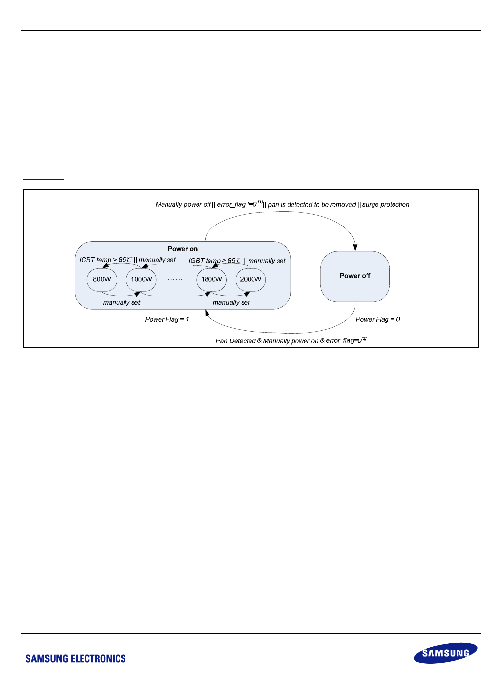
Figure 3-1 shows the state transition diagram. This diagram illustrates the operation of IH cooker system.
Figure 3-1 State Transition Diagram
After power is turned on manually, the system periodically checks for pan status and current work condition. This
ensures the power is activated only when the pan is on panel, and all temperatures and voltage are in good
condition.
The IH cooker will stop heating immediately in case of the following issues:
Manually power off by key pressing
Error flag set as temperature or voltage is abnormal
Pan is detected to be removed
Surge protection is triggered
Note that only voltage recovery can reset the error flag to ‘0’ and restart the system, which means once the error
flag is set by IGBT/Pan over-temperature, you have to restart the system manually.
In the power on state, key pressing can alter the power. For reliability, the power will automatically downgrade
when the IGBT temperature is higher than 85℃.
3-1
Page 22
S3F84B8_ALL-IN-ONE IH COOKER_AN_REV 0.00 3 SOFTWARE IMPLEMENTATION
3.2 SOFTWARE DIAGRAM
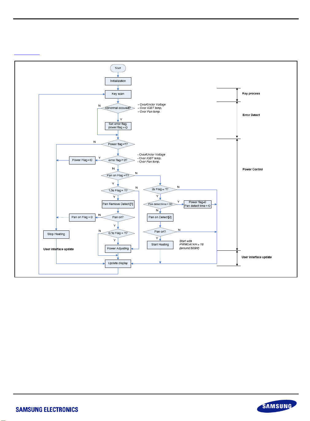
Figure 3-2 shows the software diagram.
Figure 3-2 Software Diagram
NOTE:
1. [1] Pan remove detection [1] is done by current sensing. The pan is judged to be removed when the current is lower than a
preset threshold.
2. [2] Pan on detection [2] is done by pulse counting. The pan is judged to be put on when the counted pulse number is
between 1 and 3 during 3 oscillation period.
Basic procedures include key process, error detection, power control, and UI update. These procedures are
executed as an infinite loop. Most of the processes are controlled by timing. In other words, process is executed
only when the corresponding timing flag is set. For example, 16 times AD conversion time for error detection, 1.5
second for pan-on detection, and 2 seconds for pan-remove detection.
Meanwhile, comparator1 and comparator2’s interrupts are enabled for surge protection and IGBT over-voltage
protection, separately. Therefore, the above procedure might be interrupted whenever any of the comparator 1 or
comparator 2’s interrupt condition is met.
3-2
Page 23
S3F84B8_ALL-IN-ONE IH COOKER_AN_REV 0.00 3 SOFTWARE IMPLEMENTATION
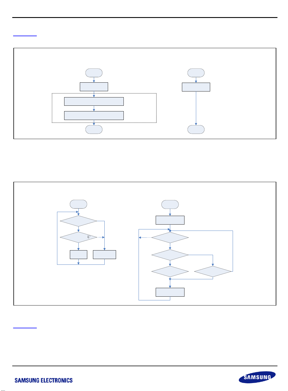
Figure 3-3 shows the flow chart of CMP1/2 interrupt service routine. Due to the cooperation of IH-PWM and
comparators integrated in S3F84B8, only a few jobs need to be done in the ISR.
CMP1INT ISR (hard lock)
For surge protection
Start
Clr pending bit
Set P0.4(PWM) to input without pull-up R
PWMCON = 0
End
Not mandatory
CMP2INT ISR (soft lock)
For IGBT over voltage protection
Start
Clr pending bit
End
Figure 3-3 Interrupt Service Routine Diagram
NOTE: When hard lock happens, the PWM returns to the safe value immediately.
When soft lock happens. The PWM returns to the safe value immediately for the current PWM cycle. And the
PWMDATA will be reloaded as PWMPDATA, usually a smaller one, from the next cycle on.
BUZ work flowFAN work flow
Start
Power flag = 0?
Y
IGBT temp < 55
Y
Fan Off
N
N
Fan On
N
Start
Beaming for 0.2s
Power flag = 1?
Y
Pan flag = 1?
No pan detected?
N
Y
Error lasts for 2s?
YY
N
Beaming for 0.2s
Figure 3-4 Fan and BUZ Workflow
Figure 3-4
shows the workflow of FAN and BUZ. FAN is always on as the IH cooker is generating heat. Even
when the device is powered off by manually setting or system protection, it is still on as long as the IGBT
temperature is higher than 55 ℃, in order to prevent the cooker from hot temperature damage.
Buzzer is mainly used for information indication. Besides the first beaming at power on, it only gives alarm when
some error lasts for 2sec or no pan is detected after trying 30 times
3-3
Page 24
S3F84B8_ALL-IN-ONE IH COOKER_AN_REV 0.00 3 SOFTWARE IMPLEMENTATION
3.3 INTERNAL RESOURCE ARRANGEMENT AND CONFIGURATION
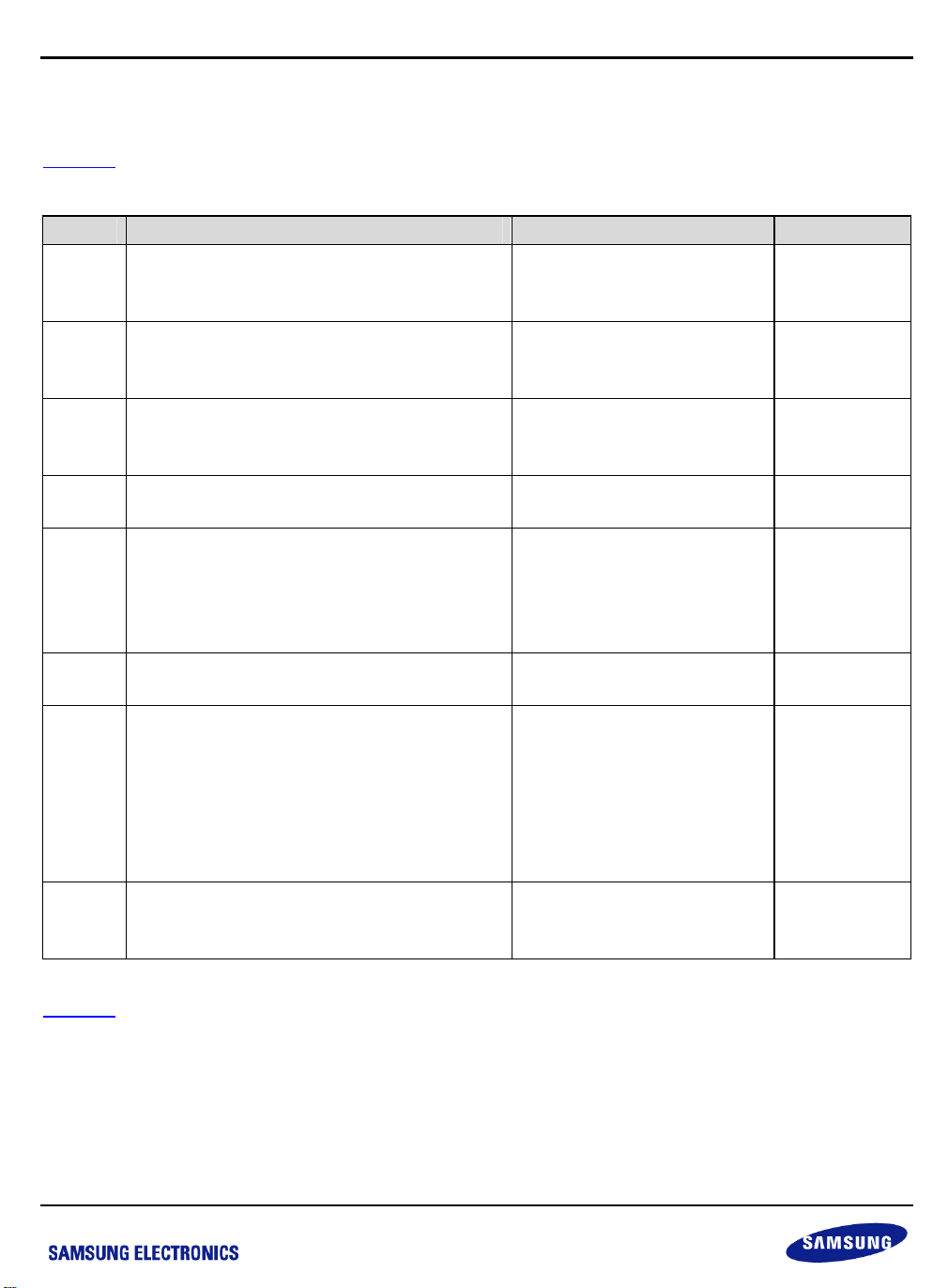
Table 3-1 shows the internal resource arrangement and configuration.
Table 3-1 Internal Resource Arrangement and Configuration
Module Purpose Configuration Registers
CMP0 Synchronization Non-inverting output
Disable INT
CMP2 Surge protection 0.50VDD reference
Non-inverting output
Enable INT
CMP1 IGBT over-V protection 0.65VDD reference,
Non-inverting output,
Enable INT
OPA Current amplification On-chip mode
PWM IGBT control Co-operate with CMP0
Delay Trigger
AMT Trigger
BUZ BUZ control 1KHz output
TA 100ms timing for
1) BUZ beaming time (0.2sec for every enable)
2) Display blink interval (0.5sec)
Internal mode
Match Interrupt Enable
TA Internal Clock = Fosc/4096
3) Error warning (BUZ) after error lasts for 2sec
4) Pan-on detect every 2sec
5) Move pan detect every 1.5sec
6) Power adjust every 0.1sec
7) Check sensor status after 3min of heating up
TC Pulse counting for pan detection Interval mode
Interrupt Disable
TC clock = CMP0_O
CMP0CON
CMPINT
P1CON
CMP1CON
CMPINT
P1CON
CMP2CON
CMPINT
P1CON
OPACON
P2CONL
PWMCON
PWMCCON
PWMDATAH/L
PWMPDATAH/L
P0CONH
BUZCON
P0CONL
TAPS
TACON
TCCON
TCPS
Table 3-1
shows the internal resource arrangement for IH cooker system and related registers in S3F84B8. For
detail description of all the registers and co-operation ways of comparators and IH PWM, refer to the S3F84B8
user’s manual.
3-4
Page 25
S3F84B8_ALL-IN-ONE IH COOKER_AN_REV 0.00 4 APPENDIX
4 APPENDIX
4.1 ERROR CODE
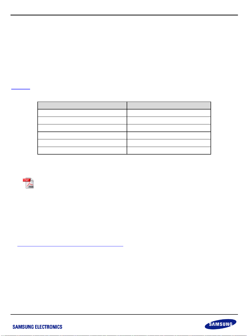
Table 4-1 shows the error information along with the error type and its code on 7seg-LED.
Table 4-1 Error Information
Error Type Error code on 7seg-LED
IGBT temperature sensor error E1
Pan temperature sensor error E2
Over voltage error E3
Under voltage error E4
IGBT over temperature error E5
Pan over temperature error E6
4.2 SCHMATIC
S3F84B8_DEMO_V0.0
_0401.pdf
4.3 SOURCE CODE
For more information about the source code, refer to the Source_Code_IHC_S3F84B8_V00.
Reference:
[1]
http://theinductionsite.com/how-induction-works.shtml
[2] S3F84B8 UM
4-1
 Loading...