

Page 1
Level
8.
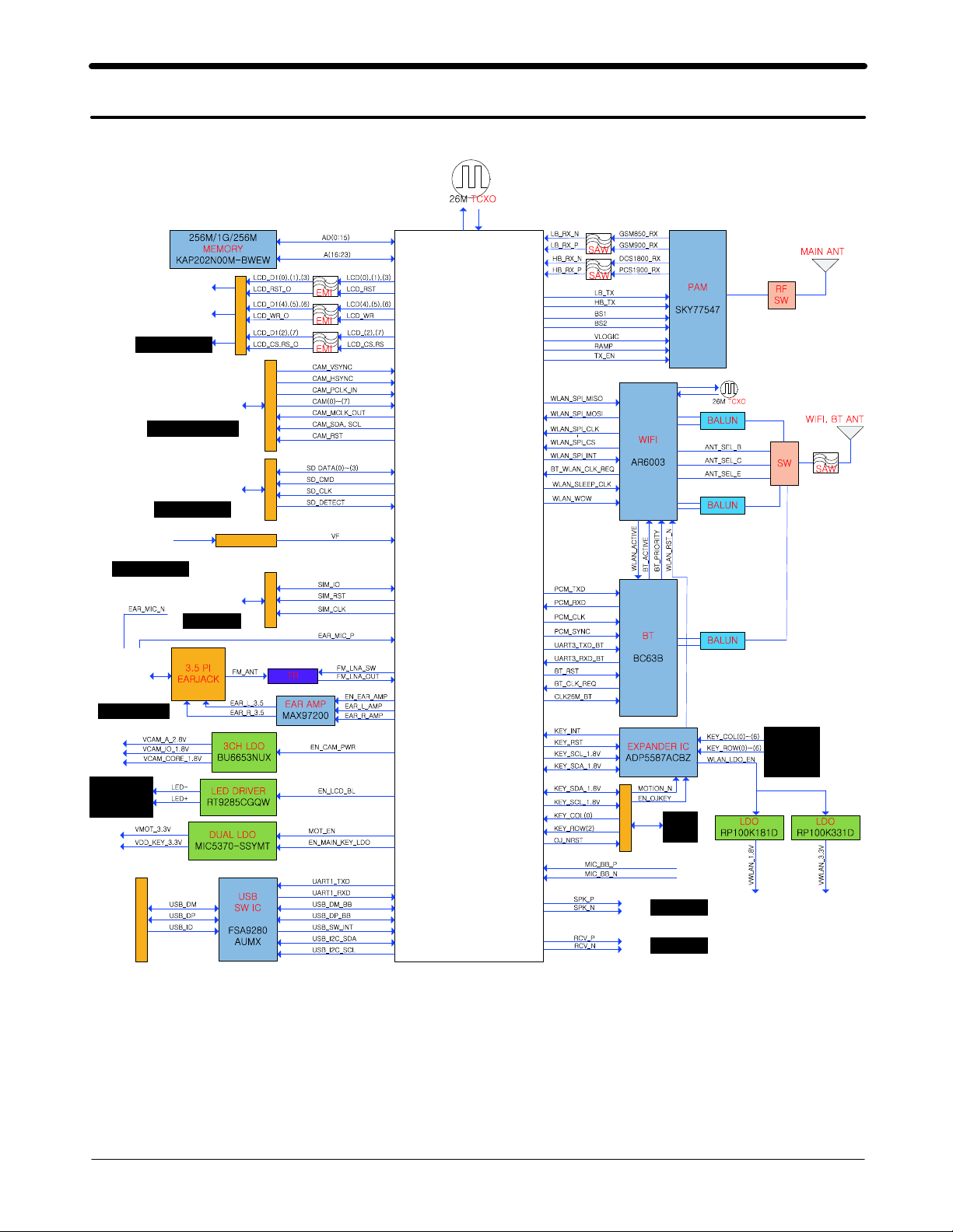
Block Diagram
8-1.
Repair
3
8-1
SAMSUNG Proprietary-Contents may change without notice
This Document can not be used without Samsung's authorization
Page 2
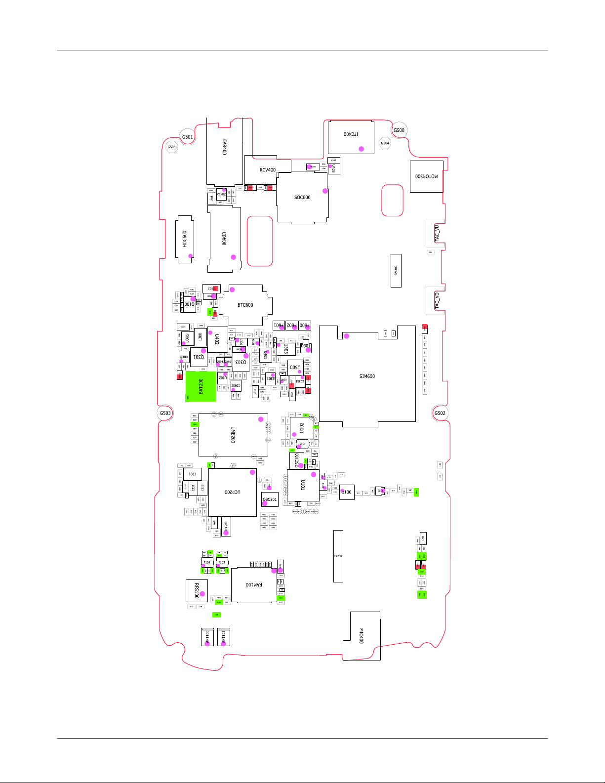
Level3Repair
PCB Diagrams
8-2.
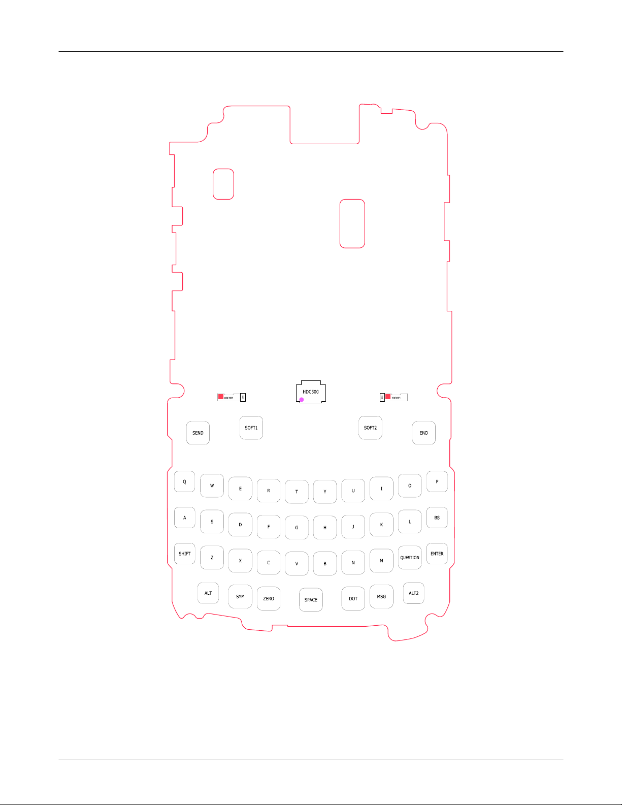
8-2-1.
Top
8-2
SAMSUNG Proprietary-Contents may change without notice
This Document can not be used without Samsung's authorization
Page 3
Level3Repair
8-2-1.
Bottom
8-3
SAMSUNG Proprietary-Contents may change without notice
This Document can not be used without Samsung's authorization
Page 4

Level3Repair
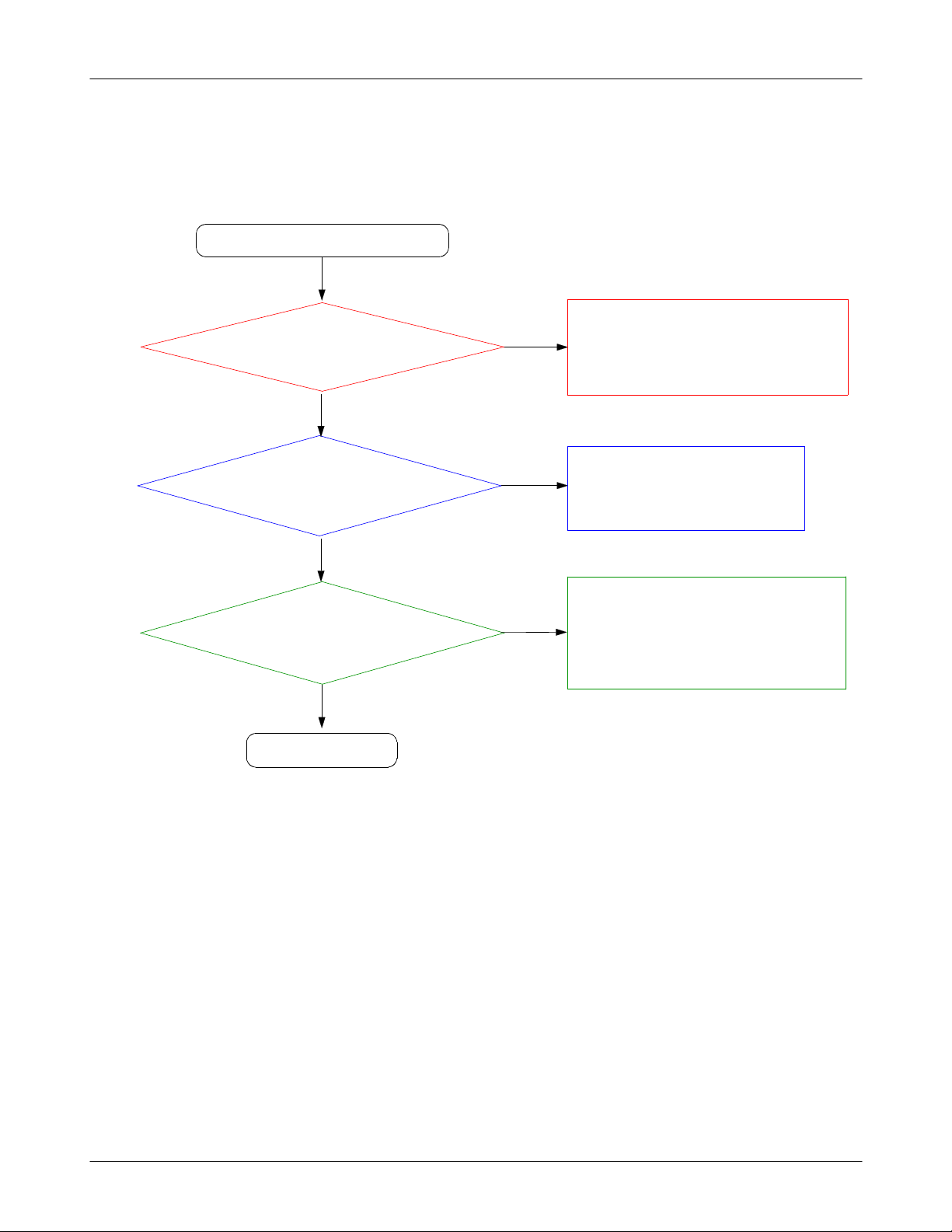
Flow Chart of Troubleshooting
8-3.
presetting methods for checking TP
※
GND&TP(exp. VBAT=
-
look over the coming out signal.
-
TA600, C603, C604
using Oscilloscope
)
GND
Oscilloscope
←
TP(Test Point)
8-4
SAMSUNG Proprietary-Contents may change without notice
This Document can not be used without Samsung's authorization
Page 5
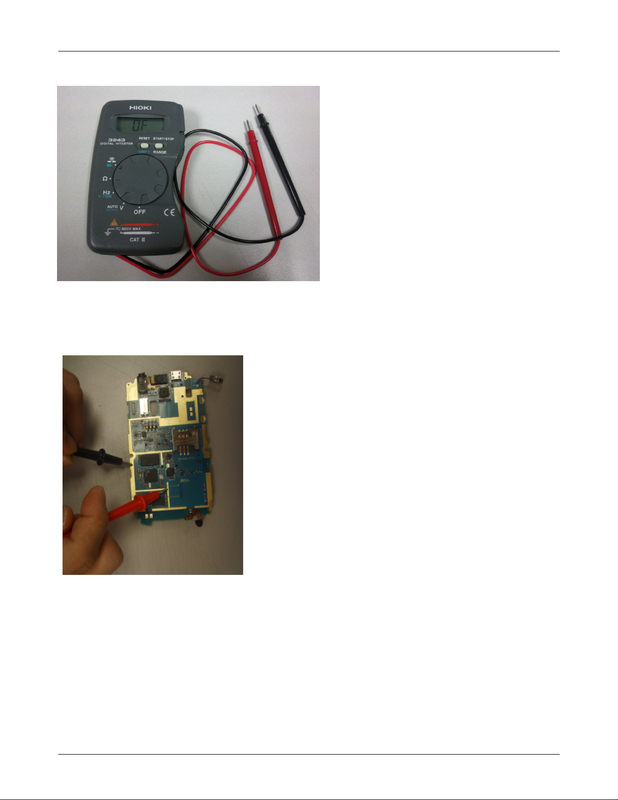
Multi-meter
←
Level3Repair
EX) to look up the TP, shunt Cap.
-
SAMSUNG Proprietary-Contents may change without notice
This Document can not be used without Samsung's authorization
Checking the TP(test point) using Multi-meter
←
if checking the GND, you can listen"beep"
-
if checking the Signal, you can't listen it.
8-5
Page 6
Level3Repair
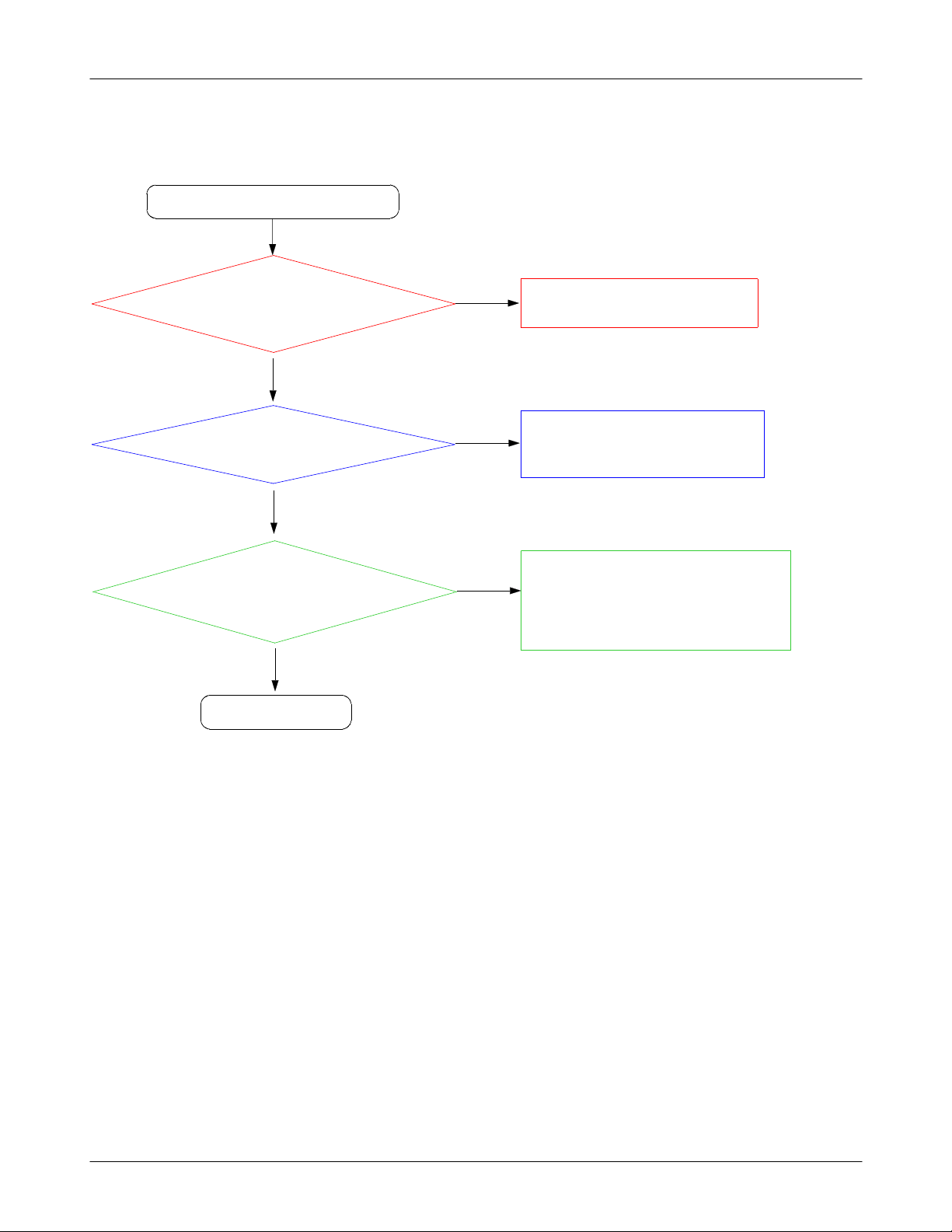
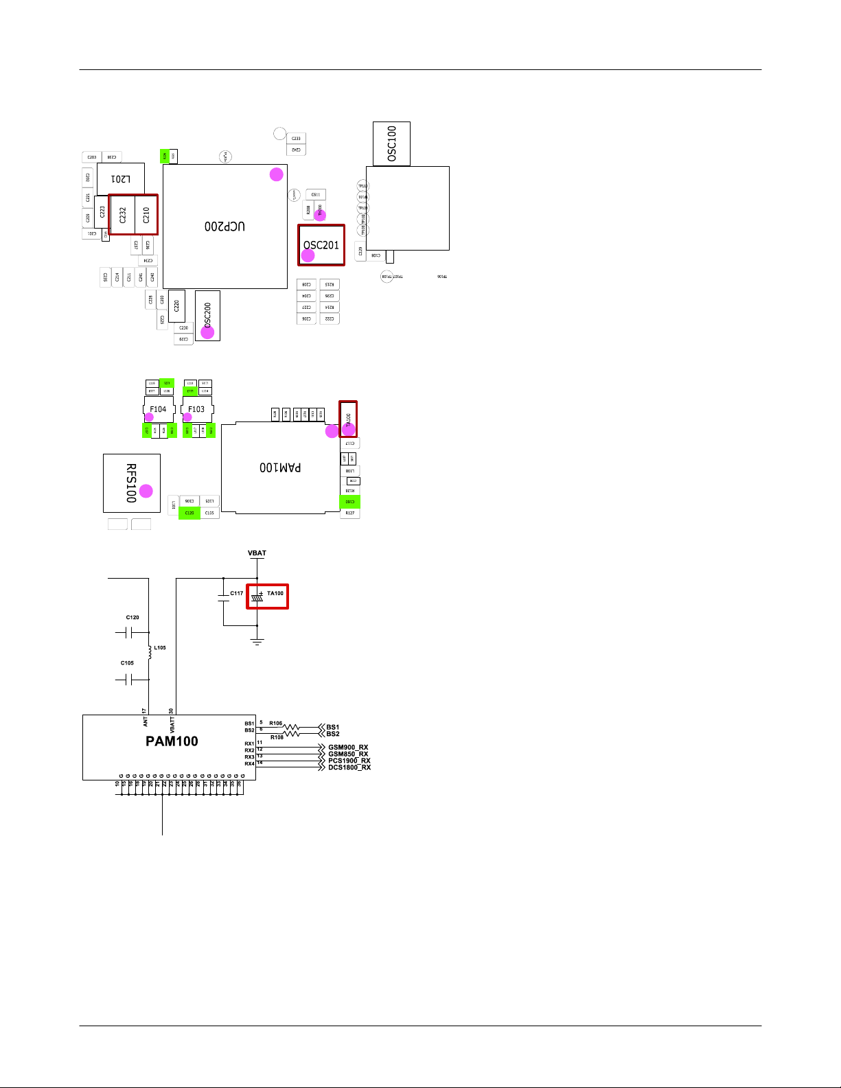
8-3-1.
Power On
Power On'does not work
'
Check the Battery Voltage
is more than
TP:TA100, C210
(
VDD_1.8V
TP: C232)
(
Check the Clock at
UCP200 A11pin
CLK26M)
(
TP:OSC201
(
Yes
Yes
=1.8
Yes
=26M
3.7V
1,3
V?
HZ
pin
No
)
No
No
)
Change the Battery
Because of batt. power low)
(
Check the Main Chip related to
SD1_FB=1.8V(TP:C232)
to look over the Chip damage)
(
Check the Main Chip
to lookover the Chip damage)
(
OSC201
(TP:
using the oscilloscope)
pin/look over the
1,3
waverform
END
Yes
8-6
SAMSUNG Proprietary-Contents may change without notice
This Document can not be used without Samsung's authorization
Page 7
Level3Repair
8-7
SAMSUNG Proprietary-Contents may change without notice
This Document can not be used without Samsung's authorization
Page 8
Level3Repair
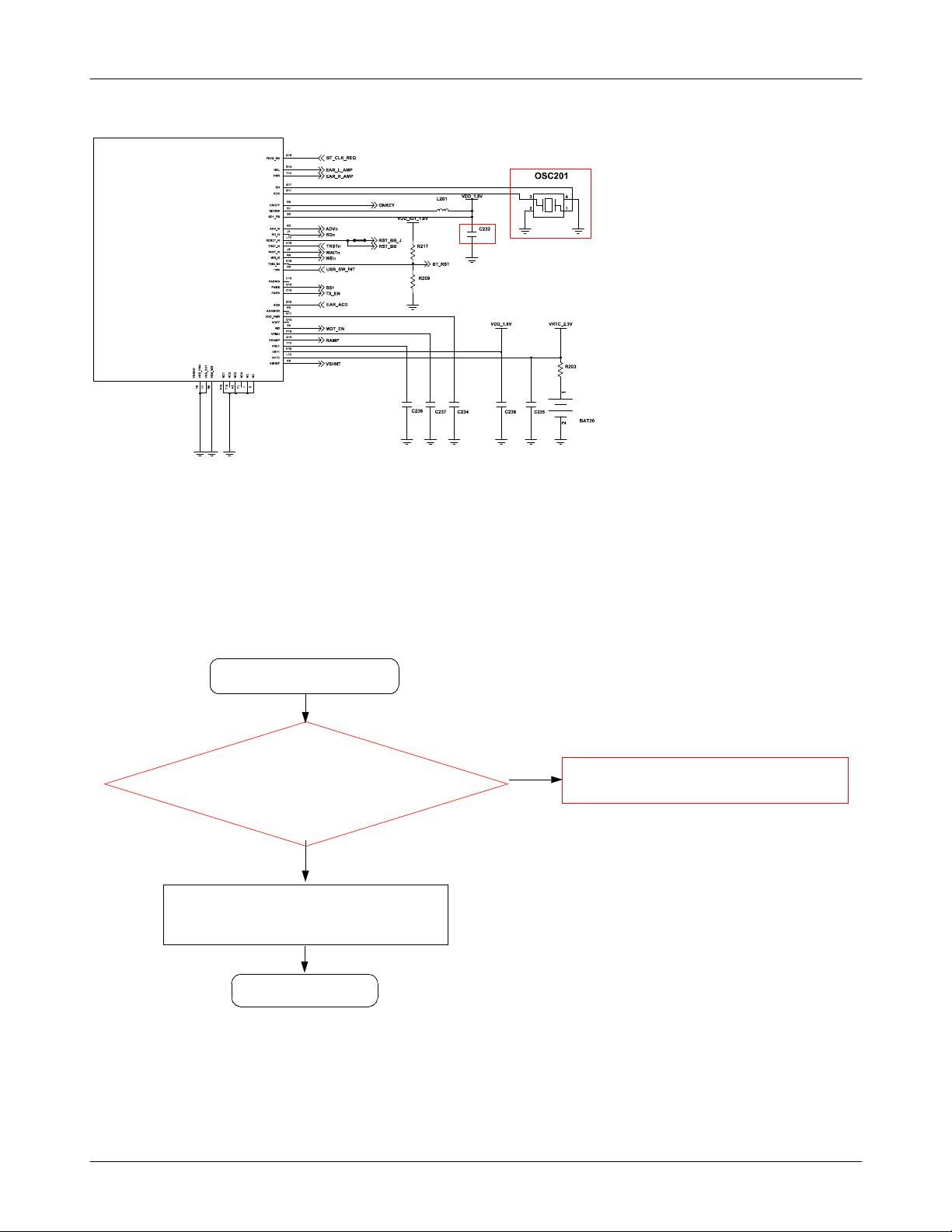
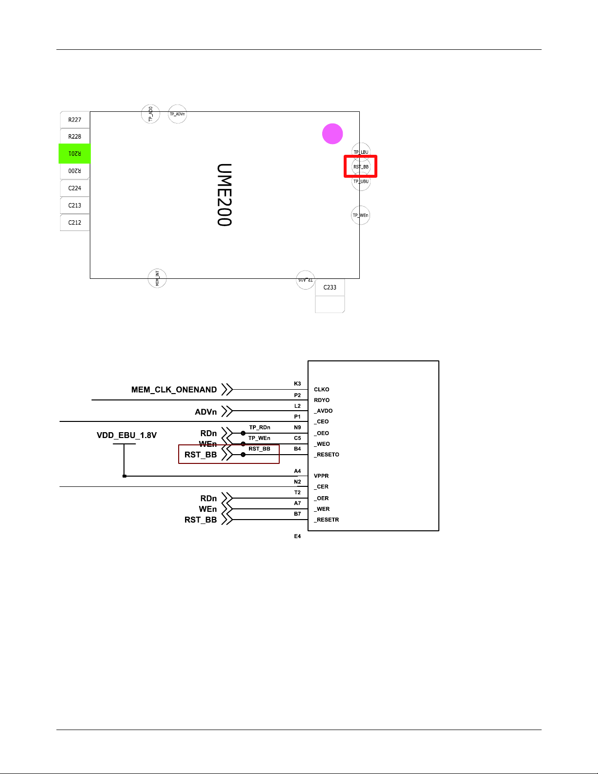
8-3-2.
Initial
Initial Failure
Yes
TP:RST_BB
using the oscilloscope GND
SHORT PAD.
Check the16bit data signals.
>1.7V?
Yes
Yes
END
&
No
Check the circuit related to reset
8-8
SAMSUNG Proprietary-Contents may change without notice
This Document can not be used without Samsung's authorization
Page 9
Level3Repair
8-9
SAMSUNG Proprietary-Contents may change without notice
This Document can not be used without Samsung's authorization
Page 10
Level3Repair
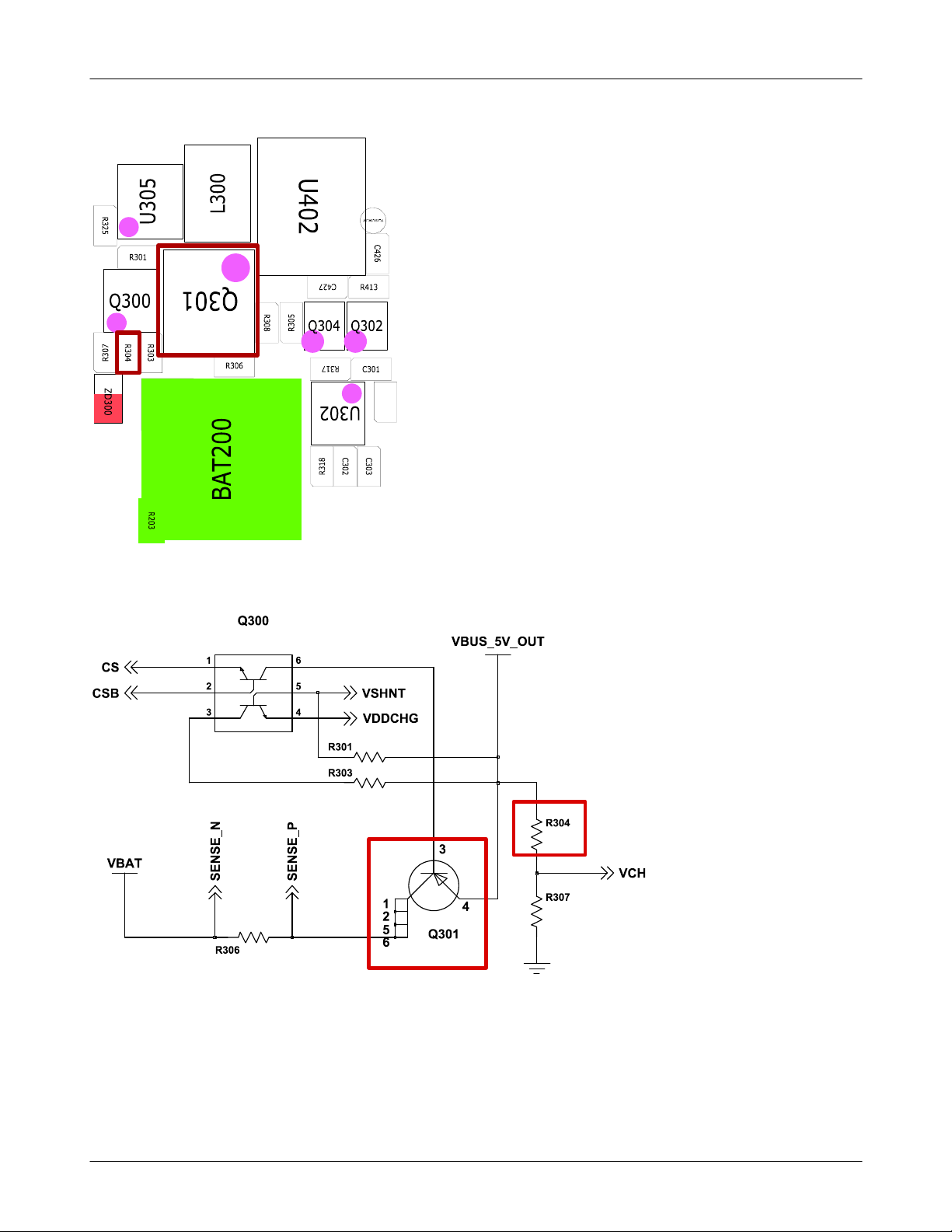
8-3-3.
Charging Part
Check the Battery&TA
Abnormal charging part
Yes
connection.
Yes
R304
> 4.9V?
Yes
No
No
be possible that it's not soldering well)
(
Reinsert the Battery or TA.
Resolder R304
Check the Q301 pin
>4.9V ?
Yes
END
4
No
Replace Q301 usingaHeatgun
8-10
SAMSUNG Proprietary-Contents may change without notice
This Document can not be used without Samsung's authorization
Page 11
Level3Repair
8-11
SAMSUNG Proprietary-Contents may change without notice
This Document can not be used without Samsung's authorization
Page 12
Level3Repair
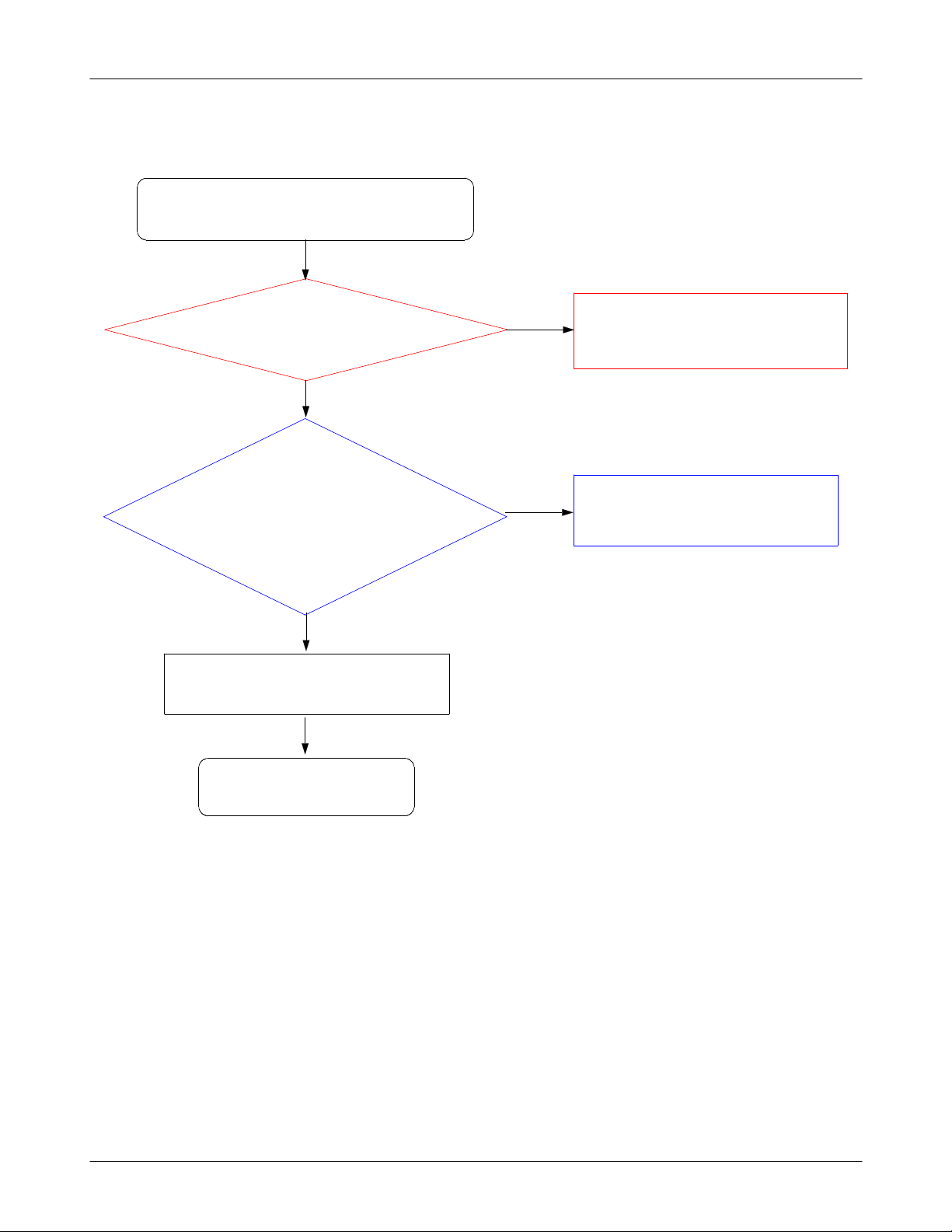
8-3-4.
Sim Part
checking its waveform using an
Phone can't access SIM Card
Yes
SIM
pin3(C608) of SIM
pin1(C606)
600
or C609
Check SIM_CLK Signal on
method:wiring pin3and
(
>2.84V?
After Power ON,
seconds.
oscilloscope)
≒
Yes
600ina
2.85V
few
No
No
Resolder C606, C609, R610
insert SIM card&access it,
then must be sim pin1 or C606
Resolder or Replace SIM600 connector.
Because of not soldering well)
(
> 2.84V
Yes
Check the SIM Card
look over if it get damaged.)
(
Yes
END
8-12
SAMSUNG Proprietary-Contents may change without notice
This Document can not be used without Samsung's authorization
Page 13

Level3Repair
8-13
SAMSUNG Proprietary-Contents may change without notice
This Document can not be used without Samsung's authorization
Page 14

Level3Repair
8-3-5.
Microphone Part
Microphone does not work
C211
at Mic Active?
Check the MIC Connection
look over schematics about
(
schemetics.)
Yes
=2.2V
Yes
Yes
No
No
Replace UCP200 usingaHeatgun
Because of not soldering well
(
Resolder L402, L403, C240, C241, C406, R400,
R402, R405, C400, C409, C415, C401,
C410, C416, C411, D400, D401
not work if those is not connected.)
(
)
Check the MIC sample.
it be possible the problem
(
things)
Yes
END
No
Replace an another MIC
because of being possible the problem)
(
8-14
SAMSUNG Proprietary-Contents may change without notice
This Document can not be used without Samsung's authorization
Page 15

Level3Repair
8-15
SAMSUNG Proprietary-Contents may change without notice
This Document can not be used without Samsung's authorization
Page 16

Level3Repair
8-16
SAMSUNG Proprietary-Contents may change without notice
This Document can not be used without Samsung's authorization
Page 17

Level3Repair
8-3-6.
Speaker Part
Speaker does not work
Wiring the SPK N/P and
(
checking an waveform using
Does not work Voice call
Yes
L400, L401
>2.0V
oscilloscope)
Yes
Yes
No
be possible because of soldering not well)
(
?
No
be possible of being UCPabad sample)
(
Resolder L400&L401
Replace UCP200 usingaHeatgun
Does not work Ringtone?
Menu->Settings->Sound
(
select the Call ringtone)
profiles
Edit->
->
Yes
Is Speaker working?
Listening through the
(
speaker)
Yes
END
No
No
Resolder or Replace UCP200, SPK400
be possible of soldering not well or being
(
UCPabad sample)
Change Speaker
be possible of SPK Problems
(
or not inserting it right.)
8-17
SAMSUNG Proprietary-Contents may change without notice
This Document can not be used without Samsung's authorization
Page 18

Level3Repair
8-18
SAMSUNG Proprietary-Contents may change without notice
This Document can not be used without Samsung's authorization
Page 19

Level3Repair
8-3-7.
Key Data Input
Check Initial Operation
When one of the keys is
pushed, is it displayed on
VDD_IO1_1.8V=1.8V?
Yes
LCD?
Yes
No
No
be possible of soldering not well or being
(
Change the Dome sheet
Resolder or Replace UCP200
UCPabad sample)
Yes
All of the key doesn't work
except POWER ON KEY
Yes
END
No
?
Replace the U500
8-19
SAMSUNG Proprietary-Contents may change without notice
This Document can not be used without Samsung's authorization
Page 20

Level3Repair
8-20
SAMSUNG Proprietary-Contents may change without notice
This Document can not be used without Samsung's authorization
Page 21

Level3Repair
8-3-8.
Back Light(for Color Main LCD)
Backlight does not work
Yes
Is LCD Contrast set on high
level in the Menu?
menu->settings->display-
(
Brightness->level
>
Is R325
Wiring U305 pin7,
(
EN_LCD_BL)
)
Yes
=1.8V?
No
No
Set LCD Contrast on high level
menu->settings->display->Brightness->level
(
select5Level(level
Resolder R325
#1 :
with an soldering iron)
(
Repalce LCD Module
#2 :
to check if it has the problem)
(
:1~5)
/
END
Yes
8-21
SAMSUNG Proprietary-Contents may change without notice
This Document can not be used without Samsung's authorization
Page 22

Level3Repair
8-22
SAMSUNG Proprietary-Contents may change without notice
This Document can not be used without Samsung's authorization
Page 23

Level3Repair
8-3-9.
Key Back Light
Main Key LED does not work
U302 pin6(C303)
look over using an
(
Oscillocope)
Key LED does not work?
look over the LED light)
(
Yes
Yes
=3.3V ?
No
No
Replace U302 usingaHeatgun
must be coming out the signal
(
Replace the LED
be possible that the sample has the problem)
(
#1 :
#2 :
Change PBA
3.3
V)
END
Yes
8-23
SAMSUNG Proprietary-Contents may change without notice
This Document can not be used without Samsung's authorization
Page 24

Level3Repair
8-24
SAMSUNG Proprietary-Contents may change without notice
This Document can not be used without Samsung's authorization
Page 25

Level3Repair
presetting
※
Rx setting)
(
Active Cell
1.
select GSM or GPRS
:
Connetion Type
2.
select Auto(GSM), BLER(GPRS)
:
BCH Parameter
3.
select measuring band(DCS or EGSM)
:
Cell power
4.
dBm
:-60
8960
Tx setting)
(
8-25
SAMSUNG Proprietary-Contents may change without notice
This Document can not be used without Samsung's authorization
Page 26

Level3Repair
After setting
※
After setting, prepare the call setup Display
1.
UsinganOriginateCall,makeacall.
2.
Confirm the display"connected"
3.
start the measuring
4.
8960 (
EGSM/DCS
)
8-26
SAMSUNG Proprietary-Contents may change without notice
This Document can not be used without Samsung's authorization
Page 27

Level3Repair
※
8960 &
spectrum analyzer
down&up at picture)
(
spectrum analyzer:testing method=the way using an Osciliscope
-
-8960:
RF Connector
connect using RF Cable between
8960 &
RF Connector in board.
8-27
SAMSUNG Proprietary-Contents may change without notice
This Document can not be used without Samsung's authorization
Page 28

Level3Repair
8-3-10.
GSM
Cell Power
PAM100
TP:L105 using
(
spectrum analyzer)
PAM100 Pin12
TP:L117 using
(
specturm analyzer)
850
RX ON
Yes
Pin
dBm
-65
Yes
dBm
-68
Yes
Receiver
:-60
17
dBm
≥
≥
No
No
Resolder PAM100, L105,C106
Check PAM100
pin
5=L,
pin6=
H
No
Yes
Check ANT Switch
control circuit
Resolder PAM100
TCXO CLOCK CHECK?
MHz@OSC201
26
Yes
Check UCP200
Yes
END
No
Resolder OSC201
8-28
SAMSUNG Proprietary-Contents may change without notice
This Document can not be used without Samsung's authorization
Page 29

Level3Repair
8-3-11.
GSM
Cell Power
PAM100
TP:L105 using
(
spectrum analyzer)
PAM100 Pin11
TP:L118 using
(
specturm analyzer)
900
RX ON
Yes
Pin
dBm
-65
Yes
dBm
-68
Yes
Receiver
:-60
17
dBm
≥
≥
No
No
Resolder PAM100, L105,C106
Check PAM100
pin
5=L,
pin6=
L
No
Yes
Check ANT Switch
control circuit
Resolder PAM100
TCXO CLOCK CHECK?
MHz@OSC201
26
Yes
Check UCP200
Yes
END
No
Resolder OSC201
8-29
SAMSUNG Proprietary-Contents may change without notice
This Document can not be used without Samsung's authorization
Page 30

Level3Repair
8-3-12.
DCS Receiver
RX ON
Cell Power
PAM100
-65
TP:L105 using
(
spectrum analyzer)
PAM100 Pin14
-68
TP:R125 using
(
specturm analyzer)
TCXO CLOCK
CHECK?
MHz@OSC201
26
:-60
Yes
Pin
dBm
Yes
dBm
Yes
dBm
17
≥
≥
No
No
No
Resolder PAM100, L105,C106
Check PAM100
pin
Resolder OSC201
5=H,
pin6=
L
No
Yes
Check ANT Switch
control circuit
Resolder PAM100
Yes
Check UCP20
Yes
END
0
8-30
SAMSUNG Proprietary-Contents may change without notice
This Document can not be used without Samsung's authorization
Page 31

Level3Repair
8-3-13.
PCS Receiver
RX ON
Cell Power
PAM100
-65
TP:L105 using
(
spectrum analyzer)
PAM100 Pin13
-68
TP:R126 using
(
specturm analyzer)
TCXO CLOCK
CHECK?
MHz@OSC201
26
:-60
Yes
Pin
dBm
Yes
dBm
Yes
dBm
17
≥
≥
No
No
No
Resolder PAM100, L105,C106
Check PAM100
pin
Resolder OSC201
5=H,
pin6=
H
No
Yes
Check ANT Switch
control circuit
Resolder PAM100
Yes
Check UCP20
Yes
END
0
8-31
SAMSUNG Proprietary-Contents may change without notice
This Document can not be used without Samsung's authorization
Page 32

Level3Repair
4
L117
1
4
R106
ANT101
ANT100
1
1
2
2
RAMP
TX_EN
LB_TX
HB_TX
RFS100
G
G
C
A
3
4
1
1
1
2
2
L100
C104
C109
2
C106
L101
C120
L105
C105
0
7
3
1
T
T
T
G
G
G
5
0
1
1
N
A
PAM100
G
G
G
G
1
9
0
8
6
2
1
2
1
1
A
B
V
G
G
G
G
G
G
G
G
2
2
8
6
5
4
3
1
2
2
2
2
2
3
R127
SHORT
R128
C160
SHORT
R105
R107
L107L106
L108
2
VLOGIC
3
VRAMP
4
TX_EN
27
GSM_IN
29
DCS|PCS_IN
G
G
G
8
7
1
9
VBAT
C117
G
G
G
4
3
2
3
3
3
TA100
5
R106
BS1
6
BS2
R108R109
11
RX1
12
RX2
13
RX3
14
RX4
G
G
6
5
3
3
BS1VLOGIC
BS2
GSM900_RX
GSM850_RX
PCS1900_RX
DCS1800_RX
GSM850_RX
GSM900_RX
DCS1800_RX
PCS1900_RX
L118
R125
R126
SHORT
SHORT
C130
C131
F103
L119
L113
L111L117
L114
L116
L120
L115
L121
LB_RX_P
LB_RX_N
HB_RX_P
HB_RX_N
1
IN1
4
IN2
G
G
5
3
2
C156C155
F104
1
IN1
4
IN2
G
G
5
3
2
C158C157
9
BAL
8
OUT
G
G
G
G
7
6
0
1
9
BAL
8
OUT
G
G
G
G
7
6
0
1
8-32
SAMSUNG Proprietary-Contents may change without notice
This Document can not be used without Samsung's authorization
Page 33

G505
Level3Repair
I
4
0
0
C
G501
0
0
6
C
D
H
C151
L
1
2
4
R
2
5
1
C147
1
1
C
9
9
4
1
C
C239
1
0
0
Q
3
2
1
L
C231
6
L
2
0
0
4
1
C
C
3
1
C315
4
6
2
3
5
R
0
3
R
3
U
2
5
R301
Q300
R
R
3
3
7
0
0
0
4
3
3
R
Z
D
3
0
0
R
2
0
3
R227
R228
0
1
0
0
C224
C213
C212
2
3
C
8
C203
C
2
0
1
2
0
2
1
2
2
C
3
2
2
2
3
9
C
0
2
2
C
C
2
0
C
1
6
1
2
C
C
2
4
3
1
5
2
C
R
F
S
1
0
0
1
0
C
9
E
A
R
4
0
0
4
1
R
6
TA400
4
1
R
RCV400
4
4
0
0
Z
Z
D
D
0
1
7
6
0
0
C418
4
4
R
R
4
1
9
ZD601
5
1
6
0
0
A
T
1
R
1
R
1
4
4
0
C143
6
C
R
1
1
6
C
6
1
0
R611
6
0
R
2
0
0
3
L
3
0
1
Q
R
3
0
8
R306
0
0
2
T
A
B
2
R
2
R
6
2
2
R
L
0
1
2
C
C
C
2
2
3
3
7
6
2
3
C
4
1
0
1
1
4
4
2
2
2
C
C
C
0
8
0
2
2
2
C
C
C
2
2
5
L
1
2
1
L116
L
1
1
9
L120
C
C
1
1
5
6
2
2
5
5
1
1
7
8
R
R
L
1
0
1
C104
0
0
1
T
N
A
C417
C
C
C
4
4
2
2
4
0
2
D
Z
1
0
8
L
L
0
4
4
0
0
4
6
5
L
L407
C
D
6
0
0
3
0
6
C
BTC600
Z
D
6
0
2
4
1
R
1
L
4
8
0
0
4
4
1
R
2
U
4
6
R
0
3
0
2
T
T
_
_
P
IN
_
B
S
U
W
S
C
4
2
6
4
2
C
7
R413
5
0
3
Q302
Q304
R
3
1
R
7
C301
R
6
5
0
0
3
0
2
U
4
6
R
C
C
ZD600
3
3
8
0
0
1
3
2
3
R
R
6
0
8
0
D
A
TP_ADVn
_
P
T
U
M
E
2
0
0
T
IN
_
M
E
M
T
P
5
_
2
R
2
D
R
n
2
0
0
P
4
3
1
C
3
0
R
6
0
7
C
C
3
1
C
2
R
4
2
3
U
3
4
9
0
0
0
3
R
C
6
4
3
0
9
U
3
0
A
T
C429
U
4
0
C433
1
C424
3
0
3
Q
C425
R418
C405
R
3
1
5
C
C
4
4
1
1
4
2
5
6
0
0
6
6
C
R
2
1
3
R
R
4
4
0
0
4
4
C
4
0
R
3
C
4
0
2
R401
2
2
2
R
TP_LBU
RST_BB
TP_UBU
TP_WEn
T
_
P
1
A
6
C233
2
4
C
2
0
T
U
O
K
C611
L
C
_
P
T
8
0
2
R
U
OSC201
2
0
C
8
2
0
C
0
2
0
2
0
C
2
C
S
O
C230
2
2
C
9
L
1
1
5
L111
L
1
1
3
L114
F103F104
C
C
1
1
7
8
5
5
1
1
5
6
1
1
L
L
1
0
C
L
6
1
0
5
C120
C105
L100
1
0
1
T
N
A
4
2
2
C
7
2
0
C
6
C
R
R
6
8
1
1
1
0
0
3
0
0
1
1
1
7
9
R
R
M
A
P
1
0
0
SOC600
6
6
0
0
F
2
1
C
4
2
2
4
3
0
C
6
1
3
C305
R
R
4
U
1
0
9
1
3
3
R
0
C
3
4
3
0
C
3
8
0
2
4
4
C
0
0
R508
R507
R316
R510
1
3
0
U
3
0
0
U
R
D
3
0
3
9
0
0
0
2
R310
0
0
3
3
R
R
C
5
0
3
C
5
0
4
1
2
2
R
C139
R
2
5
0
3
7
1
C
C
1
4
2
5
4
1
C
C
7
1
6
3
0
3
1
2
1
C
C
C123
TP110
1
T
P
0
1
0
0
TP103
2
H
T
2
0
1
P
T
0
0
1
P
T
9
2
1
C
1
0
C
8
1
C
0
7
1
8
0
2
1
R
5
2
2
C
6
2
1
R
4
2
2
C
2
R
1
0
5
0
0
1
A
T
1
1
C
7
L
1
7
0
0
6
1
L
L
1
0
8
1
C
3
0
1
2
R
8
1
6
C
0
R127
7
6
0
F
F
0
C
3
1
0
C311
7
0
3
C
D301
C
3
0
8
5
0
R
5
5
0
R
9
5
U
C500
5
0
R
6
0
0
5
5
0
1
D
Z
D
Z
Z
D
5
0
3
8
6
0
0
6
6
C
C
1
1
R
2
R113
T
1
R
0
A
_
T
1
U
P
0
0
1
T
R
A
U
_
P
T
R117
2
R217
0
2
R
0
9
1
U
C
1
3
8
C
L
1
1
F
0
1
5
2
4
2
4
R111
C140
1
R
0
4
0
0
1
9
2
1
2
1
0
1
0
C
C
C
1
C
1
S
0
0
1
1
C
1
O
C118
R
2
0
1
C132
F
U
1
F
C124
1
0
0
1
1
1
2
C
5
1
T
P
1
1
8
2
C103
1
C
9
P
T
0
1
7
T
1
T
P
P
0
4
P
0
T
1
6
0
1
TP105
P
T
F
C432
U
4
0
3
SIM600
C133
9
0
1
L
C126
7
2
1
C
1
1
1
6
C
6
U100
1
C134
CN200
M
I
C
4
0
0
G500
G504
3
0
0
R
M
O
T
O
U
V
_
C
A
T
C316
0
0
4
K
P
S
D
V
_
C
A
T
2
0
5
D
4
3
2
2
2
2
R
R
Z
C
4
0
8
0
0
4
L
L
4
0
1
7
0
4
C
C
6
0
7
9
0
6
R
C
6
0
9
R
6
1
0
G502G503
C
1
1
2
C
1
1
3
R
1
0
3
L
1
2
1
0
0
4
0
1
C
L
5
F
1
1
C
5
L
1
0
3
R
1
9
0
5
2
1
C
6
0
4
0
C
0
4
R
2
5
0
0
4
4
R
R
1
6
0
1
4
4
C
C
0
1
0
0
4
4
D
D
4
1
C
1
1
0
4
C
2
3
0
0
4
4
L
L
4
0
C
9
0
5
0
1
4
4
C
C
8-33
SAMSUNG Proprietary-Contents may change without notice
This Document can not be used without Samsung's authorization
Page 34

Level3Repair
8-3-14.
GSM
GSM900 Transmitter
850/
TX Power is too Low!!
TX ON(5Level)
TCXO CLOCK CHECK?
26
PAM100 pin
TP:R128 using
(
spectrum analyzer)
Check the Voltage
C117
MHz@OSC201
YES
27≥-4
dBm
YES
V?
<3.3
NO
NO
NO
solder OSC201
Re-
solder or change
Re-
UCP200
Check the UCP200&VBAT
circuit.
YES
PAM100
Pin
17
dBm
30
TP:L105 using
(
≥
spectrum analyzer)
YES
Check the RFS100
connection with PCB?
YES
Antenna
re-solder or change
NO
Resolder PAM100
NO
Resolder RFS100.
8-34
SAMSUNG Proprietary-Contents may change without notice
This Document can not be used without Samsung's authorization
Page 35

Level3Repair
8-3-15.
DCS/PCS Transmitter
TX Power is too Low!!
TX ON(5Level)
TCXO CLOCK CHECK?
MHz@OSC201
26
PAM100 pin
TP:L106 using
(
spectrum analyzer)
Check the Voltage
C117
dBm
<3.3
YES
29≥-4
YES
V?
NO
NO
NO
solder OSC201
Re-
solder or change
Re-
UCP200
Check the UCP200&VBAT
circuit.
YES
PAM100
Pin
17
dBm
30
TP:L113 using
(
≥
spectrum analyzer)
YES
Check the RFS100
connection with PCB?
YES
Antenna
re-solder or change
NO
Resolder PAM100
NO
Resolder RFS100.
8-35
SAMSUNG Proprietary-Contents may change without notice
This Document can not be used without Samsung's authorization
Page 36

Level3Repair
G501
G505
0
0
6
C
D
H
C151
L
1
2
4
R
2
5
5
1
C147
1
1
1
1
C
9
R
9
4
1
R
1
4
1
C
C239
1
0
0
Q
C143
3
2
1
L
C231
R
1
1
6
6
L
2
0
0
4
1
C
6
0
R
2
C
3
1
C315
4
6
2
0
3
5
R
0
0
3
3
L
R
3
U
2
5
R301
3
0
1
Q300
R
R
3
3
7
0
0
0
4
3
3
R
R306
Z
D
3
0
0
0
0
2
T
A
B
R
2
0
3
R227
R228
2
0
R
1
2
0
R
0
C224
C213
C212
2
3
C
8
C203
C
L
2
0
1
2
0
2
1
2
2
C
3
2
0
2
2
1
3
9
C
0
2
2
2
C
C
C
2
0
C
1
6
1
2
C
C
C
2
2
3
3
7
6
2
3
4
C
2
1
4
1
3
1
1
4
5
2
2
2
C
C
C
L116
C
1
5
7
R
F
S
1
0
0
1
0
C
9
C104
I
4
0
0
C
E
F
A
R
4
0
0
C432
4
1
R
6
U
4
TA400
4
1
R
7
0
RCV400
4
4
0
0
Z
Z
D
D
0
1
7
6
0
0
C418
4
4
R
R
C417
4
1
C
9
C
C
4
4
2
2
4
0
2
D
Z
1
0
8
L
L
0
4
4
0
0
4
6
5
L
L407
C
D
6
0
0
ZD601
6
0
0
A
T
3
4
0
0
6
6
C
C
BTC600
Z
C
D
6
6
1
0
0
2
R611
4
1
R
1
L
4
8
0
0
4
4
1
R
2
U
4
6
R
0
3
0
2
T
T
_
_
P
IN
_
B
S
U
W
S
C
4
2
6
4
2
C
7
Q
R413
R
3
5
0
0
8
3
Q302
Q304
R
3
1
R
7
C301
R
6
5
0
0
3
0
2
U
4
6
R
C
C
ZD600
3
3
8
0
0
1
3
2
3
R
R
6
0
8
0
D
A
TP_ADVn
_
P
T
U
M
E
2
0
0
T
IN
_
M
E
M
T
P
6
5
_
2
2
R
2
2
D
R
R
n
2
0
0
P
C
0
4
2
C
0
8
0
2
2
2
0
C
C
2
0
2
0
C
2
C
2
C
2
5
S
O
C230
2
2
C
9
L
L
1
1
1
2
5
1
L111
L
L
1
1
1
1
3
9
L114
L120
F103F104
C
C
C
1
1
1
7
8
5
6
2
2
5
5
5
1
1
1
1
5
6
8
1
1
R
R
L
L
1
0
C
L
6
1
0
5
L
1
0
1
C120
C105
L100
0
1
0
0
1
1
T
T
N
N
A
A
4
3
1
C
3
0
R
6
0
7
C
C
3
1
C
2
R
4
2
3
U
3
4
9
0
0
0
3
R
C
6
4
3
0
9
U
3
0
A
T
C429
U
4
0
C433
1
C424
3
0
3
Q
C425
R418
C405
R
3
1
5
C
C
4
4
1
1
4
2
5
6
0
0
6
6
C
R
2
1
3
R
R
4
4
0
0
4
4
C
4
0
R
3
C
4
0
2
R401
2
2
2
R
TP_LBU
RST_BB
TP_UBU
TP_WEn
T
_
P
1
A
6
C233
2
4
C
2
0
T
U
O
K
C611
L
C
_
P
T
8
0
2
R
U
OSC201
2
0
C
8
2
0
C
4
2
2
C
7
2
0
C
6
C
R
R
6
8
1
1
1
0
0
3
0
0
1
1
1
7
9
R
R
M
A
P
1
0
0
SOC600
6
6
0
0
0
F
F
2
0
1
C
4
2
2
R
4
1
0
R316
1
3
0
1
2
2
R
0
0
2
H
T
1
5
2
6
1
4
2
2
R
1
0
5
C311
4
3
0
C
6
1
3
C305
R
7
U
0
3
9
1
C
3
3
R
D301
0
C
C
3
3
4
0
3
8
0
C
3
8
0
2
4
4
C
5
0
0
U
R508
C500
R507
R510
U
3
0
0
U
R
5
0
1
D
Z
D
3
0
3
9
0
0
0
2
R310
0
0
3
3
R
R
8
6
0
0
C
6
6
5
0
3
C
5
C
C
0
4
1
1
R
2
C139
R113
R
2
5
0
3
7
1
C
2
C
1
0
4
2
1
U
5
4
1
C
C
7
1
6
1
F
0
5
3
0
3
1
2
1
C
C
C123
0
0
1
C
S
O
TP110
U
1
T
P
0
1
1
0
TP103
1
2
0
1
P
T
0
0
1
P
T
9
2
1
C
1
0
C
8
8
1
C
2
0
1
7
C
9
P
T
0
1
7
T
1
8
P
0
0
1
P
2
R
2
C
2
R
2
C
T
0
0
1
A
T
1
1
C
7
L
1
7
0
0
6
1
L
L
1
0
8
1
C
3
0
1
2
R
8
1
6
C
0
R127
3
6
F
C
3
1
0
5
0
R
5
5
0
R
9
5
0
R
6
0
0
5
D
Z
Z
D
5
0
3
T
1
R
0
A
_
T
1
U
P
0
0
1
T
R
A
U
_
P
T
R117
R217
2
R
0
9
C
1
3
8
C
L
1
1
2
4
2
4
R111
C140
1
R
0
4
9
2
1
2
1
0
1
0
C
C
1
C
1
0
0
1
1
C
1
C118
R
2
0
1
C132
F
F
C124
1
0
1
7
2
1
C
1
2
C
5
1
T
P
1
1
C103
1
T
P
0
4
P
0
T
1
6
TP105
SIM600
C133
9
0
1
L
C126
1
1
6
C
6
U100
1
M
I
C
4
0
0
C134
CN200
G500
G504
3
0
0
R
O
T
O
M
U
V
_
C
A
T
C316
0
0
4
K
P
S
D
V
_
C
A
T
2
0
5
D
4
3
2
2
2
2
R
R
Z
C
4
0
8
0
0
4
L
L
4
0
1
7
0
4
C
C
6
0
7
9
0
6
R
C
6
0
9
R
6
1
0
G502G503
C
1
1
2
C
1
1
3
R
1
0
3
L
1
2
1
0
0
4
0
1
1
C
L
5
F
1
1
C
5
L
1
0
3
R
1
9
0
5
2
1
C
6
0
4
0
C
0
4
R
2
5
0
0
4
4
R
R
1
6
0
1
4
4
C
C
0
1
0
0
4
4
D
D
4
1
C
1
1
0
4
C
2
3
0
0
4
4
L
L
4
0
C
9
0
5
0
1
4
4
C
C
8-36
SAMSUNG Proprietary-Contents may change without notice
This Document can not be used without Samsung's authorization
Page 37

ANT100
1
1
2
Level3Repair
RFS100
G
G
A
C
3
4
1
L107L106
L108
2
C106
L101
2
3
4
27
29
VLOGIC
VRAMP
TX_EN
GSM_IN
DCS|PCS_IN
C120
L105
C105
0
7
3
1
T
T
T
N
A
A
B
V
PAM100
G
G
G
G
G
G
G
G
G
5
0
1
9
1
1
7
8
G
G
G
G
0
9
8
6
1
3
2
2
1
1
1
2
2
2
G
G
G
G
G
1
5
4
8
6
3
2
2
2
2
ANT101
1
1
RAMP
TX_EN
LB_TX
HB_TX
2
2
R127
2
SHORT
L100
C104
R128
C160
SHORT
C109
R105
R107
VBAT
C117
G
G
G
3
2
4
3
3
3
TA100
5
R106
BS1
6
BS2
R108R109
11
RX1
12
RX2
13
RX3
14
RX4
G
G
5
6
3
3
BS1VLOGIC
BS2
GSM900_RX
GSM850_RX
PCS1900_RX
DCS1800_RX
C130
C131
8-37
SAMSUNG Proprietary-Contents may change without notice
This Document can not be used without Samsung's authorization
Page 38

Level3Repair
Service Schematics
8-4.
NC Point(Top View)
-
NC
:
U101
1234567891011
A
○○
B
C
D
E
F
G
H
I
J
K
L
○○○○○○○○○
○○ ○
○○ ○○○○○ ○
○ ○○○○○
○
○ ○○○○○ ○
○ ○○○○○ ○○
○○ ○○○○○ ○○
○○ ○○
○○○○○
○ ○○○○ ○
○○ ○○○
○○○○○ ○○
○○○○
U102
1234567
A
○○○
B
C
○
D
E
○○
F
G
○
H
○○
○○
○ ○○○
○○
○○ ○
○○○○○○
○○
○○○
○
○
SAMSUNG Proprietary-Contents may change without notice
This Document can not be used without Samsung's authorization
8-38
Page 39

UME200
12345678910
Level3Repair
A
B
○
C
○
D
E
F
G
H
J
K
L
M
N
P
R
○ ○○○ ○○
○○
○○ ○
○○○○○○○○○
○○○○○○○○○○
○○○○○○○○○○
○○○○○
○○○○○
○○○○ ○
○○ ○
○
T
○○○○○○○○○○
U
○○○○○○○○
8-39
SAMSUNG Proprietary-Contents may change without notice
This Document can not be used without Samsung's authorization
Page 40

Level3Repair
UCP200
ABCDEFGH I JKLMNPRT
16
○○○○○○○○○○○○○○○○
15
○○○○○○○○○○○○○○○○○
14
○○
13
○○
12
11
10
9
8
7
6
5
4
3
2
1
○○○○○○○○○○○○ ○○○
○○○○○
○○○○○○○○○○○○○○○○○
○○○○○
○○○○○○○○○○○○○○○○○
○○○○○○○○○○○○○○○○○
○○○○○○○○○○○○○○○○○
○○○○○○○○○○○○○○○○○
○○○○○○○○○○○○○
○○○○○○○○○○○○○○○○○
○○○○○○○○○○○○○○○○○
○○○○○○○○○○○○○○○○
○○○○○○○○○○○○○○
○○○○○○○○○○○○○○
○○○○○○○○○ ○
○○○○○○○○ ○○
○○○
8-40
SAMSUNG Proprietary-Contents may change without notice
This Document can not be used without Samsung's authorization
 Loading...