

Page 1
Samsung Electronics 10-1
IC Internal Diagram
10. IC Internal Diagram
10-1 74HCT245 ; AUIC4
TLF5366
MM74HCT245 Octal TRI-STATE Transceiver
August 1996
MM74HCT245
Octal TRI-STATE
Transceiver
General Description
This TRI-STATE bi-directional buffer utilizes advanced silicon-gate CMOS technology and is intended for two-way
asynchronous communication between data buses It has
high drive current outputs which enable high speed operation even when driving large bus capacitances This circuit
possesses the low power consumption of CMOS circuitry
yet has speeds comparable to low power Schottky TTL circuits
This device is TTL input compatible and can drive up to 15
LS-TTL loads and all inputs are protected from damage due
to static discharge by diodes to V
CC
and ground
The MM74HCT245 has one active low enable input (G) and
a direction control (DIR) When the DIR input is high data
flows from the A inputs to the B outputs When DIR is low
data flows from B to A
MM74HCT devices are intended to interface between TTL
and NMOS components and standard CMOS devices
These parts are also plug-in replacements for LS-TTL devices and can be used to reduce power consumption in existing designs
Features
Y
TTL input compatible
Y
TRI-STATE outputs for connection to system busses
Y
High output drive current 6 mA (min)
Y
High speed 16 ns typical propagation delay
Y
Low power 80 mA (74HCT Series)
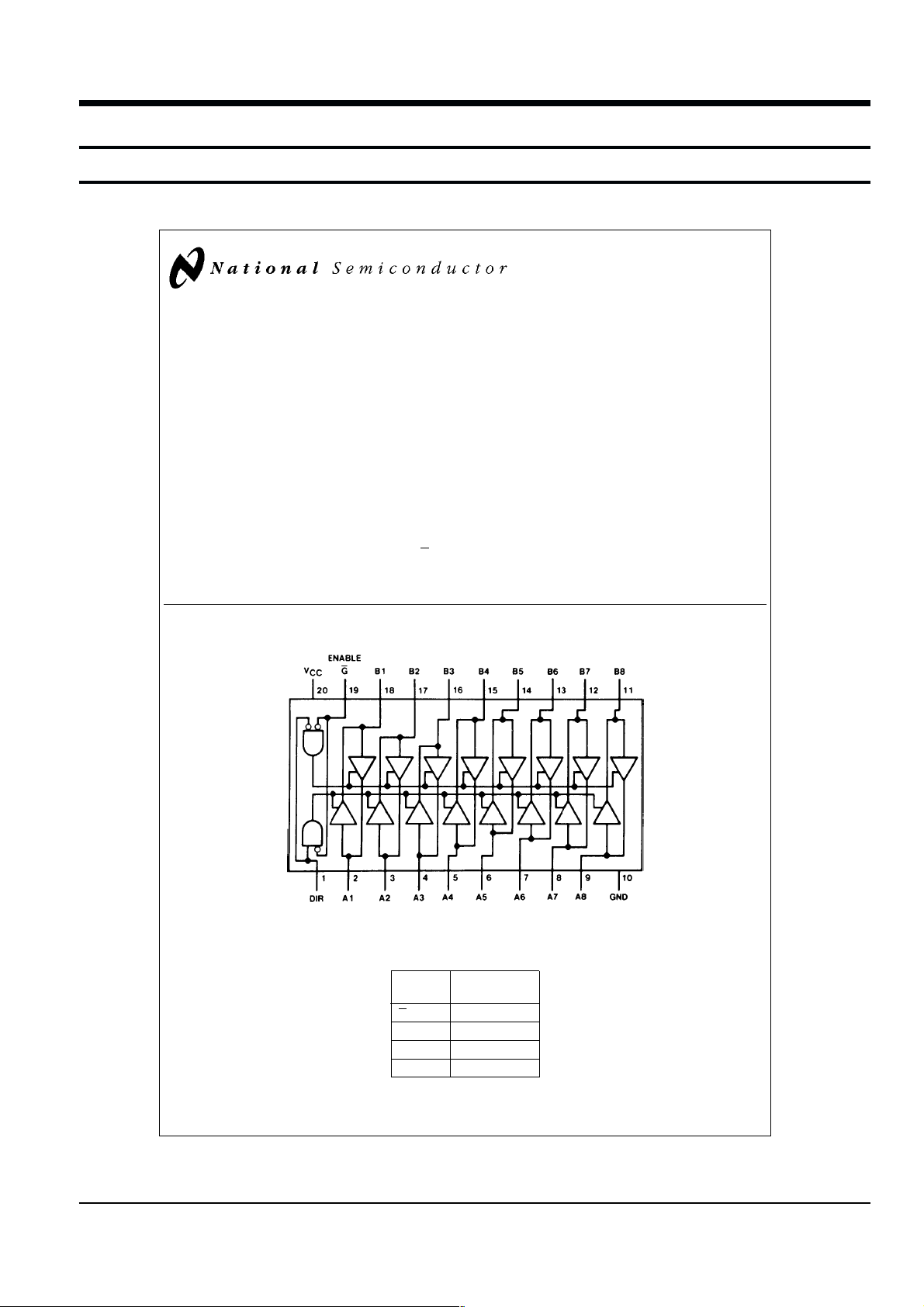
Connection Diagram
Dual-In-Line Package
TLF5366– 1
Top View
Order Number MM74HCT245
Truth Table
Control
Operation
Inputs
G DIR 245
L L B data to A bus
L H A data to B bus
H X isolation
Hehigh level Lelow level Xeirrelevant
TRI-STATEis a registered trademark of National Semiconductor Corp
C
1996 National Semiconductor Corporation RRD-B30M86Printed in U S A
httpwwwnationalcom
Page 2
10-2 Samsung Electronics
IC Internal Diagram
Absolute Maximum Ratings (Notes12)
If MilitaryAerospace specified devices are required
please contact the National Semiconductor Sales
OfficeDistributors for availability and specifications
Supply Voltage (V
CC
)
b
05 toa70V
DC Input Voltage (V
IN
)
b
15 to V
CC
a
15V
DC Output Voltage (V
OUT
)
b
05 to V
CC
a
05V
Clamp Diode Current (IIKIOK)
g
20 mA
DC Output Current per pin (I
OUT
)
g
35 mA
DC V
CC
or GND Current per pin (ICC)
g
70 mA
Storage Temperature Range (T
STG
)
b
65Ctoa150C
Power Dissipation (PD)
(Note 3) 600 mW
SO Package only 500 mW
Lead Temperature (T
L
)
(Soldering 10 seconds) 260
C
Operating Conditions
Min Max Units
Supply Voltage (V
CC
) 45 55 V
DC Input or Output Voltage 0 V
CC
V
(V
INVOUT
)
Operating Temp Range (T
A
)
MM74HCT
b
40
a
85
C
Input Rise or Fall Times
(t
rtf
) 500 ns
DC Electrical Characteristics (V
CC
e
5Vg10% unless otherwise specified)
T
A
e
25C
74HCT
T
A
e
125C
Symbol Parameter Conditions
T
A
eb
40 to 85C
Units
Typ Guaranteed Limits
V
IH
Minimum High Level 20 20 20 V
Input Voltage
V
IL
Maximum Low Level 08 08 08 V
Input Voltage
V
OH
Minimum High Level V
IN
e
VIHor V
IL
Output Voltage
l
I
OUT
l
e
20 mAV
CCVCC
b
01 V
CC
b
01 V
CC
b
01 V
l
I
OUT
l
e
60 mA V
CC
e
45V 42 398 384 37 V
l
I
OUT
l
e
72 mA V
CC
e
55V 52 498 484 47 V
V
OL
Maximum Low Level V
IN
e
VIHor V
IL
Voltage
l
I
OUT
l
e
20 mA 0 01 01 01 V
l
I
OUT
l
e
60 mA V
CC
e
45V 02 026 033 04 V
l
I
OUT
l
e
72 mA V
CC
e
55V 02 026 033 04 V
I
IN
Maximum Input V
IN
e
VCCor GND
g
01
g
10
g
10 mA
Current VIHor VILPin1or19
I
OZ
Maximum TRI-STATE V
OUT
e
VCCor GND
g
05
g
50
g
10 mA
Output Leakage G
e
V
IH
Current
I
CC
Maximum Quiescent V
IN
e
VCCor GND 8 80 160 mA
Supply Current I
OUT
e
0 mA
V
IN
e
24V or 05V (Note 4) 06 10 13 15 mA
Note 1 Absolute Maximum Ratings are those values beyond which damage to the device may occur
Note 2 Unless otherwise specified all voltages are referenced to ground
Note 3 Power Dissipation temperature derating plastic ‘‘N’’ package
b
12 mWC from 65Cto85C
Note 4 Measured per input All other inputs at V
CC
or ground
Page 3
Samsung Electronics 10-3
IC Internal Diagram
AC Electrical Characteristics MM74HCT245
V
CC
e
50V t
r
e
t
f
e
6 ns T
A
e
25C (unless otherwise specified)
Symbol Parameter Conditions Typ
Guaranteed
Units
Limit
t
PHLtPLH
Maximum Output C
L
e
45 pF 16 20 ns
Propagation Delay
t
PZLtPZH
Maximum Output C
L
e
45 pF 29 40 ns
Enable Time R
L
e
1kX
t
PLZtPHZ
Maximum Output C
L
e
5pF 20 25 ns
Disable Time R
L
e
1kX
AC Electrical Characteristics MM74HCT245
V
CC
e
50Vg10% t
r
e
t
f
e
6 ns (unless otherwise specified)
T
A
e
25C
74HCT
T
A
e
125C
Symbol Parameter Conditions
T
A
eb
40 to 85C
Units
Typ Guaranteed Limits
t
PHLtPLH
Maximum Output C
L
e
50 pF 17 23 29 34 ns
Propagation Delay
C
L
e
150 pF 24 30 38 45 ns
t
PZL
Maximum Output R
L
e
1kX
31 42 53 63 ns
Enable Time C
L
e
50 pF
t
PZH
Maximum Output R
L
e
1kX
23 33 41 49 ns
Enable Time C
L
e
50 pF
t
PHZtPLZ
Maximum Output R
L
e
1kX 21 30 38 45 ns
Disable Time C
L
e
50 pF
t
THLtTLH
Maximum Output C
L
e
50 pF 8 12 15 18 ns
Rise and Fall Time
C
IN
Maximum Input 10 15 15 15 pF
Capacitance
C
OUT
Maximum OutputInput 20 25 25 25 pF
Capacitance
C
PD
Power Dissipation (Note 5) GeV
CC
7pF
Capacitance GND G
e
100 pF
Note 5 CPDdetermines the no load power consumption P
D
e
CPDV
CC
2
faICCVCC and the no load dynamic current consumption I
S
e
CPDVCCfaICC
httpwwwnationalcom3
Page 4
10-4 Samsung Electronics
IC Internal Diagram
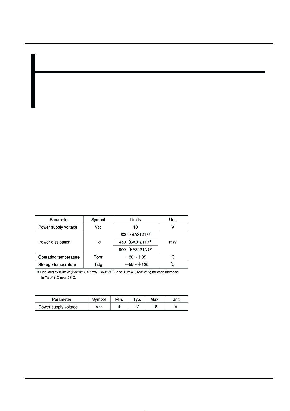
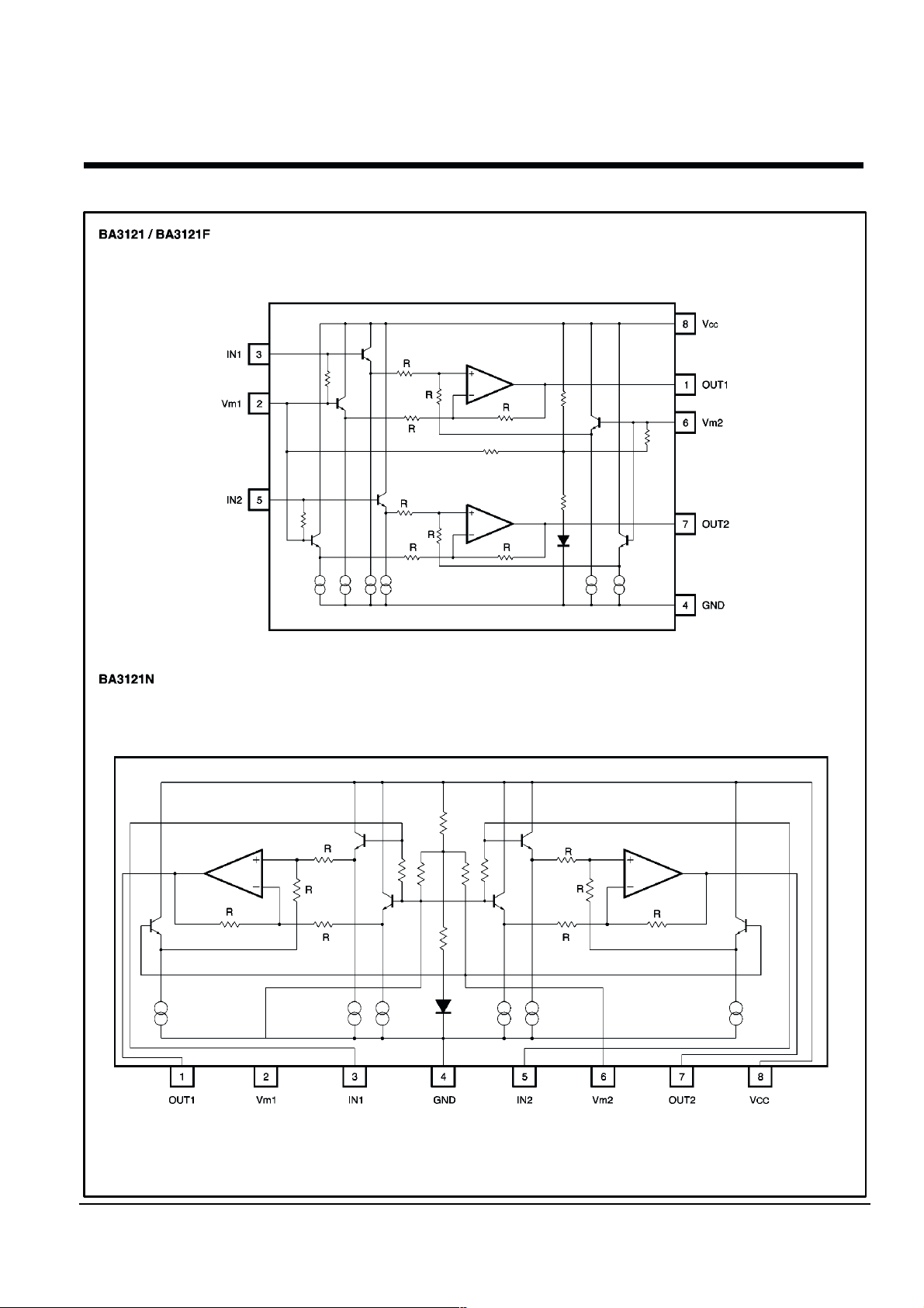
10-2 BA3121N ; AUIC2
Audio ICs
Ground isolation amplifier
BA3121 / BA3121F / BA3121N
The BA3121,BA3121F and BA3121N are ground isolation amplifiers developed for use in car audio applications. These
ICs efficiently eliminate problems caused by wiring resistance, and remove noise generated by the electrical devices
used in automobiles. The capacitance values of the external capacitors required for the ICs are small to allow compact
and reliable set design.
FApplications
Car audio systems
FFeatures
1) Large capacitors not required
2) High common-mode rejection ratio
(57dB typ. at f = 1kHz).
3) Low noise (V
NO = 3.5µVrms Typ.).
4) Low distortion (THD = 0.002% Typ.).
5) Two channels.
FAbsolute maximum ratings (Ta = 25_C)
FRecommended operating conditions (Ta = 25_C)
Page 5
Samsung Electronics 10-5
IC Internal Diagram
Audio ICs BA3121 / BA3121F / BA3121N
FBlock diagrams
Page 6
10-6 Samsung Electronics
IC Internal Diagram
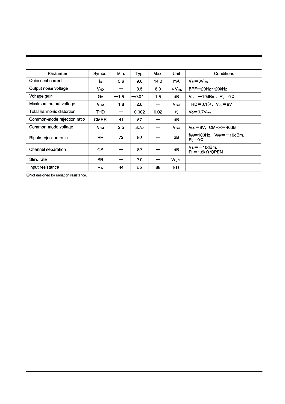
Audio ICs BA3121 / BA3121F / BA3121N
FElectrical characteristics (unless otherwise noted, Ta = 25_C, VCC = 12V, f = 1kHz, Rg = 1.8kΩ)
Page 7
Samsung Electronics 10-7
IC Internal Diagram
10-3 BQ2002 ; BIC1
Features
➤
Fast charge of nickel cadmium
or nickel-metal hydride batter
-
ies
➤
Direct LED output displays
charge status
➤
Fast-charge termination by -∆V,
maximum voltage, maximum
temperature, and maximum
time
➤
Internal band-gap voltage ref
-
erence
➤ Optional top-off charge
➤ Selectable pulse trickle charge
rates
➤ Low-power mode
➤ 8-pin 300-mil DIP or 150-mil
SOIC
General Description
The bq2002 and bq2002/F Fast-Charge
ICs are low-cost CMOS battery-charge
controllers providing reliable charge
termination for both NiCd and NiMH
battery applications. Controlling a
current-limited or constant-current
supply allows the bq2002/F to be the
basis for a cost-effective stand-alone or
system-integrated charger. The
bq2002/F integrates fast charge with
optional top-off and pulsed-trickle con
trol in a single IC for charging one or
more NiCd or NiMH battery cells.
Fast charge is initiated on application
of the charging supply or battery replacement. For safety, fast charge is
inhibited if the battery temperature
and voltage are outside configured
limits.
Fast charge is terminated by any of
the following:
n
Peak voltage detection (PVD)
n
Negative delta voltage (-∆V)
n
Maximum voltage
n
Maximum temperature
n
Maximum time
After fast charge, the bq2002/F op
tionally tops-off and pulse-trickles the
battery per the pre-configured limits.
Fast charge may be inhibited using
the INH pin. The bq2002/F may also
be placed in low-standby-power mode
to reduce system power consumption.
The bq2002F differs from the
bq2002 only in that a slightly different set of fast-charge and top-off
time limits is available. All differences between the two ICs are illustrated in Table 1.
NiCd/NiMH Fast-Charge Management ICs
bq2002/F
TM Timer mode select input
LED
Charging status output
BAT Battery voltage input
V
SS
System ground
1
PN-200201.eps
8-Pin DIP or
Narrow SOIC
2
3
4
8
7
6
5
TM
LED
BAT
V
SS
CC
INH
V
CC
TS
TS Temperature sense input
V
CC
Supply voltage input
INH Charge inhibit input
CC Charge control output
Pin Connections
Pin Names
bq2002/F Selection Guide
Part No. TCO HTF LTF
-∆V
PVD Fast Charge t
MTO
Top-Off Maintenance
bq2002
0.5 ∗ V
CC
None None
✔ C/2 160 C/32 C/64
✔ 1C 80 C/16 C/64
✔ 2C 40 None C/32
bq2002F
0.5 ∗ V
CC
None None
✔ C/2 160 C/32 C/64
✔ 1C 100 C/16 C/64
✔ 2C 55 None C/32
SLUS131–JANUARY 1999 D
Page 8

10-8 Samsung Electronics
IC Internal Diagram
Pin Descriptions
TM
Timer mode input
A three-level input that controls the settings
for the fast charge safety timer, voltage ter
mination mode, top-off, pulse-trickle, and
voltage hold-off time.
LED
Charging output status
Open-drain output that indicates the charging
status.
BAT
Battery input voltage
The battery voltage sense input. The input to
this pin is created by a high-impedance re
sistor divider network connected between
the positive and negative terminals of the
battery.
V
SS
System ground
TS
Temperature sense input
Input for an external battery temperature
monitoring thermistor.
V
CC
Supply voltage input
5.0V±20% power input.
INH
Charge inhibit input
When high, INH suspends the fast charge in
progress. When returned low, the IC resumes operation at the point where initially
suspended.
CC
Charge control output
An open-drain output used to control the
charging current to the battery. CC switch
ing to high impedance (Z) enables charging
current to flow, and low to inhibit charging
current. CC is modulated to provide top-off,
if enabled, and pulse trickle.
Functional Description
Figure 2 shows a state diagram and Figure 3 shows a
block diagram of the bq2002/F.
Battery Voltage and Temperature
Measurements
Battery voltage and temperature are monitored for
maximum allowable values. The voltage presented on
the battery sense input, BAT, should represent a
single-cell potential for the battery under charge. A
resistor-divider ratio of
RB1
RB2
= N - 1
is recommended to maintain the battery voltage within
the valid range, where N is the number of cells, RB1 is
the resistor connected to the positive battery terminal,
and RB2 is the resistor connected to the negative battery terminal. See Figure 1.
Note: This resistor-divider network input impedance to
end-to-end should be at least 200kΩ and less than 1 MΩ.
A ground-referenced negative temperature coefficient
thermistor placed near the battery may be used as a lowcost temperature-to-voltage transducer. The temperature
sense voltage input at TS is developed using a resistorthermistor network between V
CC
and VSS. See Figure 1.
bq2002/F
Fg2002/F01.eps
bq2002/F
BAT
V
SS
N
T
C
bq2002/F
V
CC
V
CC
PACK +
T
S
V
SS
BAT pin connection Thermistor connection
TM
NTC = negative temperature coefficient thermistor.
RT
R3
R4
RB1
RB2
Mid-level
setting for TM
Figure 1. Voltage and Temperature Monitoring and TM Pin Configuration
Page 9

Samsung Electronics 10-9
IC Internal Diagram
bq2002/F
Battery
Temperature?
Battery
Voltage?
Chip on
V
CC
4.0V
V
CC
2V
Top-off
LED = Z
Trickle
LED = Z
Fast
LED = Low
Maximum Time-Out
or
or
V
BAT
< 2V
V
BAT
> 2V
SD2002/F01
VTS > VCC/2 VTS < VCC/2
V
BAT
> 2V
V
BAT
> 2V
VTS < VCC/2
VTS < VCC/2
((PVD or - V or
Maximum Time-Out)
and TM = high)
(PVD or - V or
Maximum Time-Out)
and TM = high
Figure 2. State Diagram
OSC
TM
CC
LED
V
CC
V
SS
BAT
INH
Clock
Phase
Generator
Timing
Control
Sample
History
A to D
Converter
MCV
Check
TS
Bd2002f.eps
Voltage
Reference
PVD, -∆V
ALU
Power-On
Reset
TCO
Check
Power
Down
Charge-Control
State Machine
Figure 3. Block Diagram
Page 10

10-10 Samsung Electronics
IC Internal Diagram
10-4 BU1923F ; RIC1
Audio ICs
RDS / RBDS decoder
BU1923 / BU1923F
The BU1923 and BU1923F are RDS / RBDS decoders that employ a digital PLL and have a built-in anti-aliasing filter
and an eight-stage BPF (switched-capacitor filter). Linear CMOS circuitry is used for low power consumption.
FApplications
RDS / RBDS compatible FM receivers for American and European markets, car stereos, high-fidelity stereo systems
and components, and FM pagers.
FFeatures
1) Low current.
2) Two-stage anti-aliasing filter (LPF).
3) 57kHz band-pass filter.
4) DSB demodulation (digital PLL).
5) Quality indication output for demodulated data.
FAbsolute maximum ratings (Ta = 25_C)
FRecommended operating conditions (Ta = 25_C)
Page 11

Samsung Electronics 10-11
IC Internal Diagram
Audio ICs BU1923 / BU1923F
FBlock diagram
Page 12

10-12 Samsung Electronics
IC Internal Diagram
Audio ICs BU1923 / BU1923F
FPin descriptions
FInput / output circuits
Page 13

Samsung Electronics 10-13
IC Internal Diagram
10-5 LA1837 ; TIC1
Overview
The LA1837 is a single-chip AM/FM IF and MPX IC that
supports electronic tuning and was developed for use in
home stereo systems. It is optimal for use in automatic
station selection systems that use the SD and IF counting
techniques.
Functions
AM: RF amplifier, mixer, oscillator, IF amplifier,
detector AGC, oscillator buffer, S-meter, narrowband SD, IF buffer
FM IF: IF amplifier, quadrature detector, S-meter, S-
curve detector, IF buffer output
MPX: PLL stereo decoder, stereo display, forced mono,
VCO stop, post amplifier, audio muting, adjacent
channel interference rejection function
Features
• On-chip MPX VCO (no external components required)
• Adjacent channel interference rejection function
(third and fifth order)
• Supports both the SD and the IF counting techniques.
•
The AM and FM SD sensitivities can be set independently.
•
The AM and FM output levels can be set independently.
•
Improved AM practical sensitivity and high-input
distortion characteristics
Package Dimensions
unit: mm
3061-DIP30S
Monolithic Linear IC
Ordering number : EN5688
SANYO: DIP30S
[LA1837]
Single-Chip Home Stereo IC with
Electronic Tuning Support
LA1837
Parameter Symbol Conditions Ratings Unit
Maximum supply voltage V
CC
max 12 V
Allowable power dissipation Pd max Ta ≤ 70°C 550 mW
Operating temperature Topr –20 to + 70 °C
Storage temperature Tstg –40 to +125 °C
Specifications
Maximum Ratings at Ta = 25°C
Parameter Symbol Conditions Ratings Unit
Recommended supply voltage V
CC
9V
Operating voltage range V
CC
op 7 to 11 V
Operating Conditions at Ta = 25°C
Page 14

10-14 Samsung Electronics
IC Internal Diagram
No. 5688-2/9
LA1837
Parameter Symbol Conditions
Ratings
Unit
min typ max
[FM Mono Characteristics] fc = 10.7 MHz, fm = 1 kHz, with the coil adjusted so that V
AFC
– V
REG
= 0 V
Current drain I
CCO
-FM
With no input 18 31 44 mA
Demodulation output V
O
FM
100 dBµ, 100% mod. The pin 16 output 730 1100 1460 mVrms
Channel balance C.B-mono 100 dBµ, 100% mod. The pin 16 output/pin 17 output –1.5 0 +1.5 dB
Total harmonic distortion (mono) THD
FM(1)
100 dBµ, 100% mod. The pin 16 output 0.3 1.3 %
Total harmonic distortion (mono) THD
FM(2)
100 dBµ, 200% mod. The pin 16 output 1.0 5 %
Signal-to-noise ratio S/N
FM
100 dBµ, 100% mod. The pin 16 output 72 80 dB
AM rejection ratio AMR 100 dBµ, AM 30 % mod. The pin 16 output 45 65 dB
Limiting input voltage –3 dBL.S.
100 dBµ, 100% mod. Referenced to the output.
26 32 38 dBµ
The input such that the output is down –3 dB.
LED sensitivity SD
On-FM
51 60 69 dBµ
LED bandwidth SD
BW
100 dBµ 85 120 170 kHz
IF count buffer output V
IFBuff-FM
100 dBµ. The pin 13 output 80 120 160 mVrms
S-meter output
V
SM-FM(1)
0 dBµ. The pin 11 output 0 0.1 0.5 V
V
SM-FM(2)
100 dBµ. The pin 11 output 3.6 4.3 5.0 V
Muting attenuation Mute-Att 100 dBµ, 100% mod. The pin 16 output 75 85 dB
[FM Stereo Characteristics] fc = 10.7 MHz, 100 dBµ, fm = 1 kHz, L + R = 90%, Pilot = 10%
Separation (left) Sep
L
L mod. The pin 16 output/pin 17 output 30 45 dB
Separation (right) Sep
R
R mod. The pin 17 output/pin 16 output 30 45 dB
Stereo on level ST
ON
The pilot modulation such that V7 is under 0.7 V. 1.3 2.7 5 %
Stereo off level ST
OFF
The pilot modulation such that V7 is over 4.5 V. 1.5 %
Total harmonic distortion (main) THD-main L+R mod. The pin 16 output 0.3 1.3 %
Brej-3rd
fs = 113 kHz, Vs = 90 %, Pilot = 10 %, The pin
40 dB
Adjacent channel interference
16 output vs. the L-R mod. 1 kHz demodulated output
rejection ratio
Brej-5th
fs = 189 kHz, Vs = 90 %, Pilot = 10 %, The pin
40 dB
16 output vs. the L-R mod. 1 kHz demodulated output
[AM Characteristics] fc = 1000 kHz, fm = 1 kHz
Current drain I
CCO-AM
With no input 15 25 35 mA
Detector output
V
OAM(1)
23 dBµ, 30% mod. The pin 16 output 100 180 360 mVrms
V
OAM(2)
80 dBµ, 30% mod. The pin 16 output 200 320 500 mVrms
Signal-to-noise ratio
S/N
AM(1)
23 dBµ, 30% mod. The pin 16 output 18 22 dB
S/N
AM(2)
80 dBµ, 30% mod. The pin 16 output 49 55 dB
Total harmonic distortion (mono)
THD
AM(1)
80 dBµ, 30% mod. The pin 16 output 0.4 1.2 %
THD
AM(2)
80 dBµ, 80% mod. The pin 16 output 1.0 4.0 %
LED sensitivity SD
On-AM
17 27 37 dBµ
Local oscillator buffer output V
OSC-AM
With no input. The pin 30 output 110 160 220 mVrms
IF counter buffer output V
IFBuff-AM
80 dBµ, no modulation. The pin 13 output 160 220 300 mVrms
ST-IF output V
STIF-AM
80 dBµ, no modulation. The pin 7 output 16 34 48 mVrms
S-meter output V
SM-AM
0 dBµ, no modulation. 0 0 0.2 V
Electrical Characteristics at Ta = 25°C, VCC= 9 V, in the specified Test Circuit
Allowable power dissipation, Pd max – mW
Ambient temperature, Ta – °C
Pd max – Ta
Page 15

Samsung Electronics 10-15
IC Internal Diagram
Block Diagram
No. 5688-3/9
LA1837
Test Circuit Diagram
FM SD
ADJ
3 rd 5 th
DECODER
ANTI-BIRDIE
FM
Page 16

10-16 Samsung Electronics
IC Internal Diagram
10-6 KB9223
RF–
FEI
RF Amp
FDFCT
59 54 22 30 29 31 38 37 36 35 51 52 58 26 28 27 3
60
47
48
57
49
50
53
55
62
61
43
44
42
46
45
23
24
25
6
39
1
40
15 16 13 14 19 17 12 11 9 105
32
33
77
2
4
78
76
75
69
70
71
68
79
66
63
67
65
73
74
TE1
WDCH
TRCNT
LOCH
ISTAT
RESET
MLT
MDATA
MCK
ATSC
TZC
FE2
FLB
FGD
FS3
FE-
FEO
TDFCT
TE-
TEO
TE2
LPFT
TG2
TGU
SLO
SL–
SL+
SPDLO
SPDL-
SMDP
SMON
SMEF
FSET
MIRROR
MCP
FOK
GC10
GC11
CH10
CH11
MUTEI
RRC
CH20
CH21
GC21
GC20
DCC1
RFO
PD1
PD2
F
E
EI
PD
LD
VR
ARF
IRF
ASY
EFM
RFI
DCB
Focus Error Amp
FE-BIAS Adjustment
Tracking Error Amp
E/F Balance & Gain
Control
APC Amp
Center Voltage Amp.
RF Level AGC
&
Equalizer
EFM
Comparator
Defect Dectection
Circuit
Micom Data
Interface Logic
MICOM TO SERVO CONTROL
AUTO SEQUENCER
ADJUSTMENT-FREE CONTROL
FS1 to
FS4
TM to
TM6
BAL1 to
BAL5
PS1 to
PS4
GA1 to
GAS
Focus Phase
Compensation
& Offset cancel circuit
Tracking Phase
Compensation Block
& Jump Pulse GEN.
Sled Servo Amplifier
& Sled Kick GEN.
Spindle Servo LPF
(Double Speed)
MIRROR DETECTION
CIRCUIT
FOK DETECTION
CIRCUIT
Built-in Post Filter Amp (L&R)
RF Amp
Page 17

Samsung Electronics 10-17
IC Internal Diagram
10-7 KS9286
26
32
33
30
11
12
14
77
67
80
24
17
22
37
38
36
69
68
8
9
72
73
75
76
70
4
2
5
3
66
19
20
7
29
65
63
62
61
EFMI
CNTVOL
DPFIN
DPFOUT
DPDO
SMEF
SMON
SMDP
SMSD
LOCK
XOUT
XIN
MDAT
MCK
MLT
TRCNT
/ISTAT
LRCHO
ADATAO
BCKO
BCKI
ADATAI
LRCHI
EMPH
VREFL1
VREFH1
XTALSEL
TESTO
CDROM
TEST1
DATX
RCHOUT
LCHOUT
S0S1
SBCK
SDAT
SUBCODE
SYNC
DETECTOR
SUBCODE
OUTPUT
SUBCODE-Q
REGISTER
EFM
PHASE
DETECTOR
FRAME SYNC
DETECTOR
PROTECTOR
INSERTOR
EFM
DEMODULATOR
SQDT
SQCK
DIGITAL
PLL
DIGITAL
CLV
SERVO
23BIT
SHIFT
REGISTER
X-TAL
TIMING
GENERATOR
CPU
INTERFACE
TRACK
COUNTER
MODE
SELECTOR
DIGITAL
OUTPUT
ADDRESS
GENERATOR
16K
SRAM
ECC
INTERPOLATOR
DIGITAL
FILTER
& DE-EMPH
D/A
CONVERTER
8BIT DATA BUS
Page 18

10-18 Samsung Electronics
IC Internal Diagram
10-8 KA9258
28 27 26 25 24 23 22 21 20 19 18 17 16 15
1 2 3 4 5 6 7 8 9 10 11 12 13 14
GND
GND
10K
REGULATOR
10K
10K
VCC VCC
10K
10K
T • S • D
10K
10K
10K
50K
MUTE
+-
LEVEL SHIFT
-+
LEVEL SHIFT
10-9 LC72131 ; HIC1
1
22
XIN
XOUT
16
FMIN
15
AMIN
3
CE
4
DI
5
CL
6
DO
17
VDD
21
Vss
C2B
1/F
P0WER
ON
RESET
7 8 9 10
BO1 BO2 BO3 BO4
11
IO1
13
IO2
18
PD
19
AIN
20
ADUT
12
IFIN
REFERENCE
DIVIDER
PHASE DETECTOR
CHARGE PUMP
UNLOCK
DETECTOR
UNIVERSAL
COUNTER
DATA SHIFT REGISTER
LATCH
12bita PROGRAMMABLE
DIVIDER
SWALLOW COUNTER
1/16, 1/17 4D1ts
1/2
Page 19

Samsung Electronics 10-19
IC Internal Diagram
10-10 TA8207K ; AIC1
3 12
1
2
10
11
9
8
7
4
5
6
30K
45
CH2
DIAS CIACUIT
THERMAL SHUT
DOWN PROTECTION
CIRCUIT
45
30K
IN1
NF1
RIPPLB
IN2
NF2
GND
B.S.2
OUT-2
OUT-1
B.S.1
CH1
+
-
+
-
Page 20

10-20 Samsung Electronics
IC Internal Diagram
10-11 TDA7440D ; JIC1
Page 21

Samsung Electronics 10-21
IC Internal Diagram
10-12 MP3 MICOM ; AUIC3,OKI ,MSM66573 (TQFP100)
No PORT I/O PIN ASSIGN No PORT I/O PIN ASSIGN
1 P10-4 O GO 51 P0-0 I/O M-ERR
2 P10-5 O 52 P0-1 I/O M-A/F
3 P10-7 O wingo ce 53 P0-2 I/O M-STROBE
4 P8-0 I/O data I/o 54 P0-3 I/O E-SEL/IN
5 P8-1 O 55 P0-4 I/O E-INIT
6 P8-2 I/O clock 56 P0-5 I/O E-ERR
7 P8-3 O 57 P0-6 I/O E-A/F
8 P8-4 I 58 P0-7 I/O E-STROBE
9 P8-6 O 59 $ Vss
10 P8-7 O 60 P4-0 I/O E-DATA 1
11 P7-6 O 61 P4-1 I/O E-DATA 2
12 P7-7 O 62 P4-2 I/O E-DATA 3
13 VDD 63 P4-3 I/O E-DATA 4
14 Vss 64 P4-4 I/O E-DATA 5
15 P9-7 O 65 P4-5 I/O E-DATA 6
16 P9-0 INT 66 P4-6 I/O E-DATA 7
17 P9-1 INT 67 P4-7 I/O E-DATA 8
18 P9-2 O 68 P1-0 0 M-DATA 1
19 P9-3 O 69 P1-1 0 M-DATA 2
20 P6-0 INT wingo request 70 P1-2 0 M-DATA 3
21 P6-1 INT 71 P1-3 O M-DATA 4
22 P6-2 INT 72 P1-4 O M-DATA 5
23 P6-3 INT 73 P1-5 O M-DATA 6
24 P6-4 I/O E-P/CONTROL 74 P1-6 O M-DATA 7
25 P6-5 I/O E-BLANK 75 P1-7 O M-DATA 8
26 P6-6 I/O 76 P2-O O e-data/IN1
27 P6-7 I/O 77 P2-1 O e-data/out1
28 P5-4 I/O 78 P2-2 O e-data/OUT2
29 P5-5 I/O 79 P2-3 O e-data/in2
30 P5-6 I/O 80 $ Vdd
31 P5-7 I/O 81 $ Vref(VDD)
32 /RESET IN I RST_ IN 82 A/D P12-0 I
33 NM1 NMI(VCC) 83 A/D P12-1 I
34 /EA /EA(VDD) 84 A/D P12-2 I
35 VDD 85 A/D P12-3 I
36 XT0(GND) 86 A/D P12-4 I
37 XTI 87 A/D P12-5 I
38 GND 88 A/D P12-6 I
39 OSC0 89 A/D P12-7 I
40 OSCI 90 $ Vss
41 VDD 91 P7-0 O
42 P11-0 O 92 P7-1 O
43 P11-1 O 93 $ Vss
44 P11-2 O 94 P7-2 O
45 P11-3 O 95 P7-4 O
46 P11-6 O 96 P7-5 O
47 P11-7 O 97 P10-0 I/O CLK
48 P3-1 I 98 P10-1 O DATA OUT
49 P3-2 I 99 P10-2 I DATA IN
50 P3-3 O 100 P10-3 O DIR
Page 22

10-22 Samsung Electronics
IC Internal Diagram
10-13 SLIM MICOM ; UIC3
PORT NO NAME IO FUNCTION PORT NO NAME IO FUNCTION
P 16 1 MCE MYMP3 CE VP 51 VPP O -32V
P 17 2 POWER O POWER ON/OFF S20 52 O VFD SEG 14 RDS
P3 0 3 MO/ST I FM MONO/STEREO S21 53 O VFD SEG 13 BACKUP
1 4 TUNED I TUNED S22 54 O VFD SEG 12
2 5 A/MU O AUDIO MUTE S23 55 O VFD SEG 11
3 6 DI I LC72131 DI( PCB->DO ) S24 56 UD8 O VFD SEG 10
4 7 CE O LC72131 CHIP ENABLE S25 57 UD7 O VFD SEG 9
5 8 CLK O LC72131/TDA7440 CLOCK S26 58 UD6 O VFD SEG 8
6 9 DO O LC72-/TDA- DO (PCB->DI) S27 59 UD5 O VFD SEG 7
7 10 RDS I RDS DATA OUT S28 60 UD4 O VFD SEG 6
P70 11 RDS I RDS CLK S29 61 UD3 O VFD SEG 5
RES 12 RESET MICOM RESET S30 62 UD2 O VFD SEG 4
P74 13 CF1 I 32.768 KHz IN S31 63 UD1 O VFD SEG 3
P75 14 CF2 O 32.768KHz OUT S32 64 O VFD SEG 2
VSS 15 GND GND S33 65 S18 O VFD SEG 1
CF 1 16 XT1 I 6MHZ OSC IN 2 66 OPT I OPTION INPUT
CF 2 17 XT2 O 6MHZ OSC OUT 3 67 I
VDD1 18 VDD VDD 4 68 I
P8 0 19 LKFS I LKFS 5 69 I
1 20 FOK I FOK 6 70 I
2 21 TRCNT I TRCNT 7 71 I
3 22 SENSE I SENSE & LIMIT SW VDD4 72 VDD4 VFD 5V
4 23 AD1 I KEY A/D 1 PF 0 73
5 24 AD2 I KEY A/D 2 1 74
6 25 AD3 I KEY A/D 3 2 75 CLOSM O CLOSE MOTOR
7 26 CHARG I CHARGBE BATTERY 3 76 OPENM O OPEN MOTOR
P7 1 27 SCE I MYMP3 REQUEST 4 77 PLED O P SOUND LED
2 28 SCOR I SCOR IN 5 78 EQLED O EQ LED
3 29 REMO I REMOCON IN 6 79 SNLED O SNOOE LED
S 0 30 S0 O 7 80 T_CNT TUNER/CD CONTROL
1 31 S1 O PG 0 81 O
232S2O 1 82 O
333S3O 2 83 O
4 34 S4 O VFD GRID 1 3 84 O
5 35 S5 O VFD GRID 2 PO 0 85 MCK 0 MCK
6 36 S6 O VFD GRID 3 1 86 XRST O RESET
7 37 S7 O VFD GRID 4 2 87 MDATA O DATA
8 38 S8 O VFD GRID 5 3 88 MLT O MLT
9 39 S9 O VFD GRID 6 VSS2 89 GND
10 40 S10 O VFD GRID 7 VDD2 90 VDD2
11 41 S11 O VFD GRID 8 P0 4 91 MY-S I “MY-MY,MP3 SENSE”
12 42 S12 O 5 92 P_SEN I POWER SENSE
13 43 S13 O 6 93 SW2 I CLOSE SW
14 44 S14 O 7 94 SW1 I OPEN SW
15 45 S15 O P1 0 95 CMUTE O CD MUTE
VDD3 46 VDD3 VFD 5V 1 96 SQDT I SUBQ DATA IN
S 16 47 S16 O VFD SEG18 TUNER 2 97 SQCK O SUBQ DATA IN CLK
17 48 S17 O VFD SEG17 TUNER 3 98 PCTL O P-SOUND ON/OFF
18 49 S18 O VFD SEG16 TUNER 4 99 SDADA I/O SYTEM DATA I/O
19 50 S19 O VFD SEG15 12/24 HR 5 100 SCLOCK O SYSTEM CLOCK
 Loading...