

查询S1T8825B供应商
1.3GHZ DUAL PLL S1T8825B
INTRODUCTION
16−TSSOP−0044
The S1T8825B is a high performance dual frequency synthesizer with
two integrated high frequency pre-scalers for RF operation up to 1.3
GHz.
The S1T8825B is composed of modulus pre-scalers providing 64 and
66, no dead-zone PFD, selectable charge pump current, selectable
power down mode circuits, lock detector output, and loop filter’s time
constant switch.
It is fabricated using the ASP5HB Bi-CMOS process and is available
16-TSSOP with surface mount plastic packaging. Serial data is transferred into the S1T8825B via three-wire interface (CK, DATA, EN).
FEATURES
• Two systems for receiver and transmitter
• Very low operating current consumption: Icc = Typ. 7.0mA @ 3.0V
• Low operating power supply voltage : 2.2 to 5.5V ( 200MHz to 550MHz Operating )
2.7 to 3.6V ( 550MHz to 1.3GHz Operating )
• Modulus pre-scaler: 64 / 66
• No dead-zone PFD
• Colpitts type local oscill ati on
• Selectable charge pump current
• Selectable power down mode
• TSSOP 16-pin package (0.65 mm pitch)
ORDERING INFORMATION
Device Package Operating Temperature
+S1T8825B01-R0B0 16−TSSOP−0044 −30 °C to + 85 °C
+: New Product
APPLICATIONS
• Cordless telephone syst ems
• Portable wireless communications (PCS)
• Wireless Local Area Networks (WLANs)
• Other wireless communication systems
1
S1T8825B 1.3GHZ DUAL PLL
BLOCK DIAGRAM
1
Fin1
V
2
CC
CP1
3
GND
4
LD
5
CK
6
DATA
7
EN
8
PIN CONFIGURATION
Pre_Amp 1/2
Charge
Pump
Phase
Detector
Lock
Detector
Control
Circuit
2
6
Prescaler
1
32, 33
Buffer
Channel 1
Program-
able
Divider
17 12
Prescaler
1
32, 33
Buffer
Channel 2
Program-
able
Divider
Reference
Divider
1/2 Pre_Amp 16
15
2
Charge
Pump
Phase
Detector
Switch
Local
OSC
1/2
Buffer
14
13
12
11
10
Fin2
CP2
OSCI
OSCO
9
V
CC
GND
SW
BO
Fin1
V
CC
CP1
GND
LD
CK
DATA
EN
1
2
3
4
KB8825
5
6
7
8
S1T8825B
16
15
14
13
12
11
10
Fin2
V
CC
CP2
GND
SW
OSCI
OSCO
9
BO
16TSSOP
2
1.3GHZ DUAL PLL S1T8825B
PIN DESCRIPTION
Pin No. Symbol I/O Description
1 Fin1 I Input terminal of channel 1 RF signal.
2, 15 Vcc − Power supply voltage input. PIN2 and PIN15 are connected together.
3 CP1 O Output terminal of channel 1 charge pump. Charge pump is constant current output
circuit, and output current is selected by input serial data.
4, 13 GND − Terminal of GND. PIN4 and PIN13 are connected together.
5 LD O Output terminal of lock detection. It is the open drain output.
6 CK I Input terminal of clock.
7 DATA I Input terminal of data.
8 EN I Input terminal of enable signal.
9 BO O Output terminal of buffer amplifier. The signal of local oscillation is output through the
buffer amplifier.
10 OSCO O Output terminal of local oscillation signal.
11 OSCI I Input terminal of local oscillation signal.
In case of external input, connecting it to this terminal.
12 SW O Switch-over terminal for the time constant of loop filter. It is an open drain output.
If you don’t switch the time constant of loop filter, general output is available.
14 CP2 O Output terminal of channel 2 charge pump. Charge pump is a constant current output
circuit, and the output current is selected by input serial data.
16 Fin2 I Input terminal of channel 2 RF signal.
ABSOLUTE MAXIMUM RATINGS
Characteristic Symbol Value Unit
Power Supply Voltage Vcc 6 V
Power Dissipation P
Operating temperature T
Storage temperature T
Take care ! ESD sensitive device
D
OPR
STG
600 mW
−30 to + 85 °C
−55 to +150 °C
3
S1T8825B 1.3GHZ DUAL PLL
ELECTRICAL CHARACTERISTICS
(Ta = 25°°°°C, VCC = 3V, unless otherwise specified)
Characteristic Symbol Test Conditions Min. Typ. Max. Unit
Operating power supply
voltage
Operating cu rrent
consumption
Standby current I
V
I
Fin1=Fin2= 200MHz — 550MHz 2.2 3.0 5.5 V
CC
Fin1=Fin2= 550MHz — 1.3GHz 2.7 3.0 3.6 V
Fin1=Fin2=1.3GHz/ -5dBm input 5.5 7.0 9.5 mA
CC
Standby mode − 010µA
SB
Fin operating frequency Fin Fin1 = Fin2 = − 5dBm 200 − 1300 MHz
Vcc=2.2V − 15 − 0
Fin1 = Fin2
= 200MHz
Vcc=3.0V − 15 − 0
Vcc=5.5V − 10 − 0
Vcc=2.2V −15 − 0
Fin input sensitivity Fin
Fin1 = Fin2
= 550MHz
Vcc=3.0V −15 − 0
dBm
Vcc=5.5V − 10 − 0
Vcc=2.7V − 10 − 0
Fin1 = Fin2
= 1.3GHz
Vcc=3.0V − 10 − 0
Vcc=3.6V − 10 − 0
OSCI operating frequency F
osc
V
= 0dBm, sinewave
Fin
5-25MHz
Vcc = 2.2V − 10 0 5
OSCI input voltage
Serial data input high
voltage (CK, DATA, EN)
Serial data input low voltage
(CK, DATA, EN)
Charge pump output
current
Charge pump leakage I
V
V
V
I
CP1
I
CP2
I
CP3
I
CP4
CPL
f
= 10MHz
osc
Vcc = 3.0V − 10 0 5
Vcc = 5.5V - 5 0 5
osc
f
osc
= 20MHz
Vcc = 2.2V − 10 0 5
Vcc = 3.0V − 10 0 5
Vcc = 5.5V − 50 5
−
V
IH
V
= 2.2 to 5.5V
CC
V
IL
= 2.2 to 5.5V
CC
CC
0.4
− -V
−−0.4 V
CP1 = 0, CP2 = 0 VCP = 1.5 V – ± 1.6 − mA
CP1 = 1, CP2 = 0 VCP = 1.5V – ± 0.2 − mA
CP1 = 0, CP2 = 1 VCP = 1.5V −± 0.4 − mA
CP1 = 1, CP2 = 1 VCP = 1.5V −± 0.8 − mA
Standby mode, Vcp = 1.5V −1 −+1 µA
dBm
4
1.3GHZ DUAL PLL S1T8825B
FUNCTIONAL DESCRIPTIONS
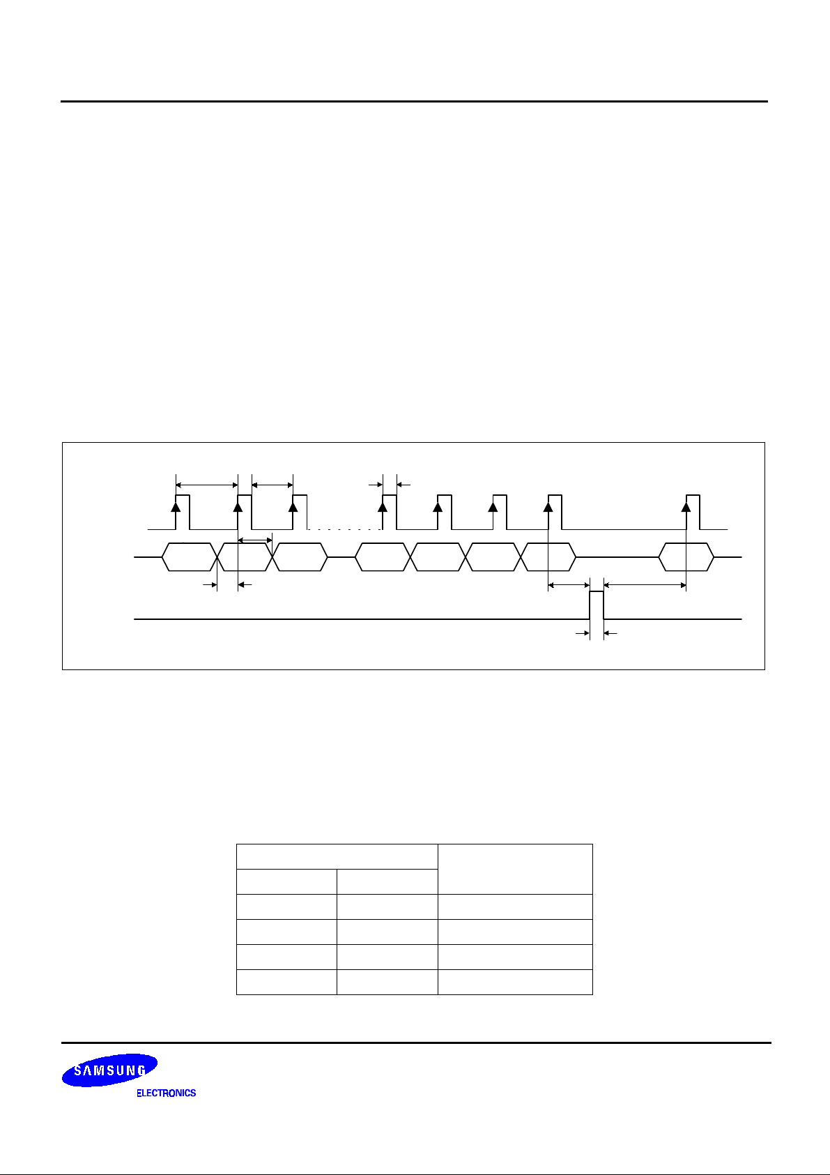
SERIAL DATA INPUT AND TIMING
CK (Pin6), DATA (Pin7), EN (Pin8) terminals in S1T8825B are used for MCU serial data interface (LSB: 1st input
data; MSB: Last input data). Serial data controls the programmable reference divider, programmable divider (CH1),
programmable divider (CH2), and control latch separately by means of group code. Binary serial data is entered via
the DATA pin.
One bit of data is shifted into the internal shift register on the rising edge of the clock. When EN pin is high, stored
data is latched. The three terminals, CK, DAT A, and EN, contain Schmitt trigger circuits to keep the data from errors
caused by noise, etc.
< Notice >
1. When power supply of S1T8825B is disconnected, CLK, DATA, EN port from MCU should be pulled low.
2. When power goes up first, R counter data should be entered earlier than N1 and N2 counter data.
3. When power goes up first, control data should be entered earlier than N1 and N2 counter data.
≥
≥
≥
0.2us
≥
≥
0.1us
≥
0.2us
LSB MSB
≥≥
≥≥
0.1us 0.2us
0.2us
≥
≥
DATA
EN
CK
≥
1us 0.2us
LSB MSB LSB
MSB
N1 (R1) N2 (R2) N3 (R3) N16 (R11) N17 (R12) GC2 GC1
Figure 1.
NOTE: Start data input with LSB first
SERIAL DATA GROUP AND GROUP CODE
The S1T8825B can be controlled through 4 kinds of group selection. Each group is identified by selective a 2-bit
group code given below.
Serial Bits Group Location
GC1 (MSB) GC2 (MSB-1)
0 0 Control Latch
0 1 Ch 1 N Latch
1 0 Ch 2 N Latch
1 1 OSC R Latch
5

S1T8825B 1.3GHZ DUAL PLL
CONTROL LATCH
The control register executes the following functions:
• Mode selection (H: test mode, L: normal mode)
• Charge pump’s polarity and output current selection for each channel.
• Output state selection for Lock Detector.
• Standby control of each channel and reference divider.
• ON / OFF control in filter switch.
CH1 CH2LSB
T CP CP1 CP2 CP1SB1 SB2CP2 SBR LD1 LD2 SW
MSB
GC2
"0"
Group Code
GC1
"0"
Figure 2.
Bit Bit 1 Bit 2 Bit 3 Bit 4 Bit 5 Bit 6 Bit 7
Name T CP CP1 CP2 SB1 CP1 CP2
Description test mode charge
pump
output
polarity
channel 1
charge
pump
output
current
channel 1
charge
pump
output
current
channel 1
standby
channel 2
charge
pump
output
current
channel 2
charge
pump
output
current
Bit Bit 8 Bit 9 Bit 10 Bit 11 Bit 12 Bit 13 Bit 14
Name SB2 SBR LD1 LD2 SW GC2 GC1
Description channel 2
standby
6
reference
divider
standby
lock
detector
control 1
lock
detector
control 2
filter switch group code
“0”
group code
“0”

1.3GHZ DUAL PLL S1T8825B
CHARGE PUMP OUTPUT POLARITY (CP)
In normal operation, the CP should be “0”.
In reverse operation, the CP should be “1”.
Depending upon VCO characteristics, CP should be set accordingly;
When VCO characteristics are like (1), CP should be set to low
When VCO characteristics are like (2), CP should be set to high.
CHARGE PUMP OUTPUT CURRENT (CP1, CP2)
The S1T8825B includes a constant current output type charge pump circuit.
Output current is varied according to control bit “CP1” and “CP2”.
In order to get high speed lock-up, select the best charge pump output current.
Control Bit Charge Pump
CP1 CP2
Output Current
00± 1600 µA
01± 200 µA
10± 400 µA
11± 800 µA
VCO
Output
Frequency
VCO Characteristics
(1)
(2)
VCO Input Voltage
7

S1T8825B 1.3GHZ DUAL PLL
TEST MODE AND LOCK DETECTOR OUTPUT (T, LD1, LD2)
When T is normal “0”, LD (Pin5) state is varied by controlling “SB1”, “SB2”, “LD1” and “LD2”.
When T is high “1”, LD (Pin5) state is changed to be useful for test
T SB1 SB2 LD1 LD2 LD Output State
00 low
0
0
1
0
0
1
1
10
0 1 channel2
1 0 channel1
1 1 channel1. AND. channel2
00 low
0 1 high
1 0 channel1
1 1 channel1
00 low
0 1 channel2
1 0 high
1 1 channel2
00 low
0 1 high
1 0 high
1 1 high
00 low
0 1 pres2
10 fpll2
11 fref
1
01
11×× low
00×× low
8
00 div4
0 1 pres1
10 fpll1
1 1 fosc/2

1.3GHZ DUAL PLL S1T8825B
LOCK DETECTOR OUTPUT
When the phase comparator detects a phase difference, LD (Pin5) outputs “L”.
When the phase comparator locks, LD outputs “H”. On standby, it outputs “H”.
When T is less than 2/fosc (T<2 /fosc ) for more than three cycles of reference divider output as in the figure below,
the lock detector outputs “H”.
BA
Reference
Divider output
Channel
Divider output
T
Charge pump
output
Lock detector
output
Figure 3. Lock Detector Output
T<2/fosc
fosc: OSCI operating frequency (LOCAL OSC).
T: time difference of the pulse between reference divider output and channel divider output.
A =
B =
Number of divisions by reference divider
fosc
2
(s)
fosc
(s)
PROGRAMMABLE STANDBY MODE (SB1, SB2, SBR)
Standby mode can be controlled by 3-control bits such as SB1, SB2 and SBR. SB1 and SB2 can control the
standby mode of channel 1 and channel2. The “SBR” bit can do ON / OFF control of reference divider.
Control Bit Standby Mode State
SB1 SB2 SBR CH1 CH2 REF Mode Status
00× ON ON ON Inter locking Mode
01× ON OFF ON CH1 Locking Mode
10× OFF ON ON CH2 Locking Mode
1 1 0 OFF OFF ON REF On Mode
1 1 1 OFF OFF OFF Standby Mode
9

S1T8825B 1.3GHZ DUAL PLL
FILTER SWITCH CONTROL (SW)
The operation mode of the SW terminal is set by bit “SW”.
SW control is useful for switching the time constant of the loop filter.
Output type of this terminal is an open drain output. High lock mode or normal lock mode can be used, taking
advantage of filter switch control (SW) with the charge pump output current.
When fast lock function can’t be used, normal lock mode is available.
Control Bits Operation Mode (SW and LPF example) The third order LPF
SW CP1 CP2
000
001
Normal Lock Mode
010
011
100
CP1
SW
R
R
R
101
High Lock Mode
110
GND
111
CRYSTAL OSCILLATOR CIRCUIT (OSCI, OSCO) AND BUFFER OUT (BO)
External capacitors C1, C2, C3, and C4 are required to set the proper crystal’s load capacitance and oscillation
frequency as shown in figure 4. The value of the capacitors is dependent on the crystal chosen.
The BO (Pin9) outputs local oscillation signal with buffer amplifier.
This terminal (Pin9) can be applied to the 2nd mixer input
C4
10
OSCI
OSCO
BO
C1
1000pF
C3
C2
2'nd MIX
or OPEN
OSCI
OSCO
BO
Figure 4.
1000pF
1000pF
Reference Oscillator
2'nd MIX
or OPEN

1.3GHZ DUAL PLL S1T8825B
PROGRAMMABLE REFERENCE COUNTE R
This block generates the reference frequency for the PLL.
The reference divider is composed of 12-bit reference divider and a half fixed divider
Sending certain data to the reference divider allows the setting of any of 6 to 8190 divisions (multiple of two)
.
LSB MSB
R = R1 × 2
R1 R2 R3 R4 R5 R6 R7 R8 R9 R10 R11 R12
0
+ R2 × 2
1
+ … + R12 × 2
11
GC2
"1"
Group CodeDivision Ratio of the R counter, R
GC1
"1"
Division ratio: 2 × R = 2 × (3 to 4095) = 6 to 8190
Data is shifted in LSB first.
Division
R12R11R10R9R8R7R6R5R4R3R2R1
Ratio
3 000000000011
4 000000000100
• ••••••••••••
4095 111111111111
Example) A 21.25MHz X-tal oscillator is connected, and divided into 25kHz steps.
(Reference frequency is 12.5kHz)
21.25 MHz ÷ 12.5 kHz = 1700
1700 = 2 × R
R = (850)
= (1101010010)
10
2
0 1 0 0 1 0 1 0 1 1 0 0 1 1
MSBLSB
11

S1T8825B 1.3GHZ DUAL PLL
CHANNEL 1, CHANNEL 2 PROGRAMMABLE N COUNTER
These programmable dividers are composed of a 5-bit swallow counter (5-bit programmable divider),
12-bit programmable main counter, and two-modulus prescalers providing 64 and 66 divisions.
Sending certain data to the swallow counter and the 12-bit programmable main counter allows the setting of any of
2048 to 262142 divisions (multiple of two).
The 12-bit programmable divider and swallow counter are set by each channel;
each channel is identified by a group code.
LSB
N1 N2
Swallow counter
N3 N4 N5 N6 N7 N8 N9 N10 N11 N12 N13 N14 N15 N16 N17 N18 N19
Division Ratio of the N Counter, N
Figure 5.
5-BIT SWALLOW COUNTER DIVISION RATIO (A COUNTER)
A = N1 × 2
0
+ N2 × 2
Division ratio: 0 to 31, B ≥ A
1
… N5 × 2
4
Division Ratio
(A)
0 00000
1 00001
• •••••
31 11111
main counter
N5 N4 N3 N2 N1
MSB
Group Code
CH1 = "10"
CH2 = "01"
12-BIT MAIN COUNTER DIVISION RATIO (B COUNTER)
B = N6 × 2
0
+ N7 × 21 + N7 × 2
2
… N17× 2
11
Division ratio: 3 to 4095
Data is shifted in LSB first
Division
Ratio (B)
N17 N16 N15 N14 N13 N12 N11 N10 N9 N8 N7 N6
3 000000000011
4 000000000000
• ••••••••••••
4095 111111111111
12

1.3GHZ DUAL PLL S1T8825B
Channel1 and 2 Programmable Counter Division Ratio, N
N = 2 × (32 × B + A), B ≥ A
Division ratio: 192 to 262142
Example) A Signal of 453 MHz is entered into Fin1, and divided into 25 kHz steps.
(Reference frequency is 12.5 kHz)
453 MHz ÷ 12.5 kHz = 36240, N = 2 × (32 × B + A) = 36240 , 32 × B + A =18120
N = 18120 ÷ 32 = 566.25, A = 0.25*32 = 8
∴ B = (566)
= (1000110110)2, A = (8)
10
= (01000)
10
2
LSB
0
0 0 1 0 0 1 1 0 1 1 0 0 0 1 0 0 1 0
MSB
Example) A Signal of 462.9 MHz is entered into Fin2, and divided into 25 kHz step.
(Reference frequency is 12.5 kHz)
462.9 MHz ÷ 12.5 kHz = 37032, N = 2 × (32 × B + A) = 37032, 32 × B + A =18516
N = 18516 ÷ 32 = 578.625, A = 0.625*32 = 20
∴ B = (578)
= (1001000010)2, A = (20)
10
LSB
0
0 1 0 1 0 1 0 0 0 0 1 0 0 1 0 0 0 1
= (10100)
10
2
MSB
PHASE DETECTOR AND CHARGE PUMP CHARACTERISTICS
Phase difference detection Range: -2 π to +2 π
When SW = Low
CP
LD
f
r
f
p
O
fr > f
fr = f
p
fr < f
p
fr < f
p
fr < f
p
p
Figure 6.
13

S1T8825B 1.3GHZ DUAL PLL
SENSITIVITY TEST CIRCUIT
2.2 V to 5.5 V
51 ohm
50 ohm
RF
Signal Generator
Oscilloscope
Microstrip
V
CC
5 kohm
1000pF
1
Fin1
5
LD
6
CK
7
DATA
8
EN
VCC
OSCI
OSCO
2.15
10 nF
11
100p
10
+
10 uF
20.945 MHz
SERIAL
DATA
UNIT
68p 50p
47p
14

1.3GHZ DUAL PLL S1T8825B
TYPICAL APPLICATION CIRCUIT
10nF
VCO
2.2k
0.1µF
51k
10nF
V
CC
1nF
10nF
50pF 47pF
8.2k
20.945
MHz
68p
2n'd MIX
1nF
100p
10uF
16
Fin2
Fin1
1
+
1nF
VCO
MOD
15
V
CC
V
CC
2
10nF
7.5k
CP1
CP2
3
14
10nF
30k
10nF
13
GND
S1T8825B
KB8825
GND
4
0.1µF
SW
LD
12
5
11
OSCI10OSCO
CLK
5k
V
CC
9
BO
DATA
6
7
EN
8
From
Controller
15

S1T8825B 1.3GHZ DUAL PLL
NOTES
16
 Loading...