
查询S1M8831A供应商
FRACTIONAL-N RF/INTEGER-N IF DUAL PLL S1M8831A/33
INTRODUCTION
24-QFN-3.5×4.5
The S1M8831A/33 is a Fractional-N frequency synthesizer with integrated
prescalers, designed for RF operation up to 1.2GHz/K-PCS and for IF
operation up to 520MHz. The fractional-N synthesizer allows fast-locking,
low phase noise phase-locked loops to be built easily, thus having rapid
channel switching and reducing standby time for extended battery life. The
S1M8831A/33 based on ∑ - ∆ fractional-N techniques solves the fractional
spur problems in other fractional-N synthesizers based on charge pump
compensation. The synthesizer also has an additional feature that the
PCS/CDMA channel frequency in steps of 10kHz can be accurately
programmed.
The S1M8831A/33 contains dual-modulus prescalers. The S1M8831A RF
synthesizer adopts an 8/9 prescaler (16/17 for the S1M8833) and the IF
synthesizer adopts an 8/9 prescaler. Phase detector gain is user-programmable for maximum flexibility to
address IS-95 CDMA and IMT2000. Various program-controlled power down options as well as low supply
voltage help the design of wireless cell phones having minimum power consumption.
Using the Samsung's proprietary digital phase-locked-loop technique, the S1M8831A/33 has a linear phase
detector characteristic and can be used for very stable, low noise PLLs. Supply voltage can range from 2.7V to
4.0V. The S1M8831A/33 is available in a 24-QFN package.
FEATURES
• High operating frequency dual synthesizer
— S1M8831A: 0.71 to 1.2GHz(RF)/ 45 to 520MHz(IF)
— S1M8833: 1.6 to 1.65GHz(RF)/ 45 to 520MHz(IF)
• Operating voltage range: 2.7 to 4.0V
• Low current consumption (S1M8831A: 5.0mA, S1M8833: 7.0mA)
• Selectable power saving mode (ICC = 1uA typical @ 3V)
• Dual-modulus prescaler and Fractional-N/Integer-N:
— S1M8831A (RF) 8/9 Fractional-N
— S1M8833 (RF) 16/17 Fractional-N
— S1M8831A/33 (IF) 8/9 Integer-N
• Excellent in-band phase noise ( – 85dBc/Hz @ PCS, -90dBc/Hz @CDMA)
Improved fractional spurious performance ( < 80dBc)
• Frequency resolution (= 10kHz/64 @ fref = 9.84MHz)
• Fast channel switching time: < 500us
• Programmable charge pump output current: from 50uA to 800uA in 50uA steps
• Programmability via on-chip serial bus interface
1

S1M8831A/33 FRACTIONAL-N RF/INTEGER-N IF DUAL PLL
APPLICATIONS
• High-rate data-service cellular telephones (for CDMA): S1M8831A, S1M8833
• High-rate data-service portable wireless communications (for Korean-PCS): S1M8833
• Other wireless communications systems
ORDERING INFORMATION
Device Package Operating Temperature
+S1M8831A01-G0T0
+S1M8833X01-G0T0
+ : New Product
24-QFN-3.5×4.5
-40 to +85C
2
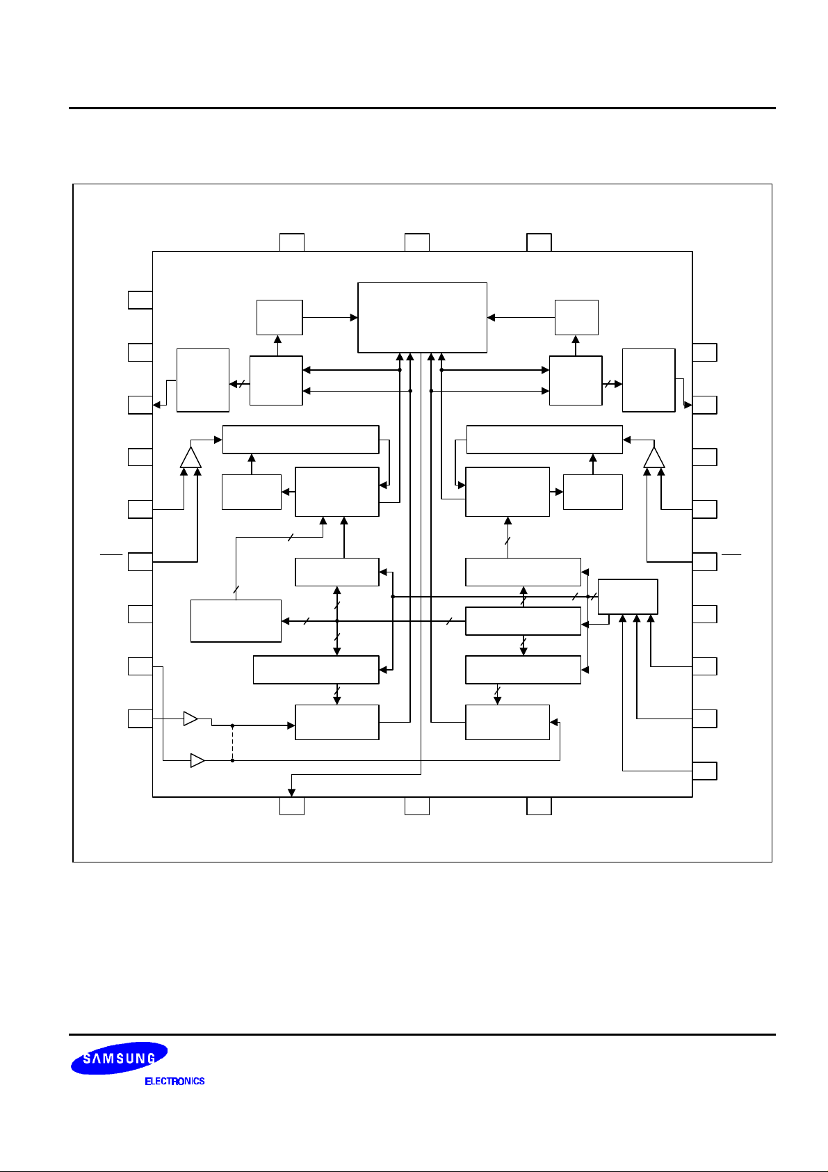
FRACTIONAL-N RF/INTEGER-N IF DUAL PLL S1M8831A/33
BLOCK DIAGRAM
OUT0 OUT1 VDDIF
24 23 22
VDDRF
VPRF
CPORF
DGND
finRF
finRF
GND
OSCx
1
RF
LD
2
RF
Charge
3
Pump
RF
Phase
Detector
RF Prescaler
4
5
6
+ -
Prescaler
Control
RF
Programmable
Counter
RF N-Latch
foLD Data Out
Multiplexer
IF Prescaler
IF
Programmable
Counter
IF N-Latch
IF
LD
IF
Phase
Detector
Prescaler
Control
IF
Charge
Pump
- +
21
20
19
18
17
VPIF
CPOIF
DGND
finIF
finIF
2-Bit
7
RF
8
Frac-N Latch &
Σ−∆
Modulator
RF R-Latch
24-Bit Shift Register
IF R-Latch
Control
16
15
GND
LE
IF
OSCin
9
RF Reference
Counter
IF Reference
Counter
14
13
DATA
CLOCK
10 11 12
foLD RF_EN IF_EN
3
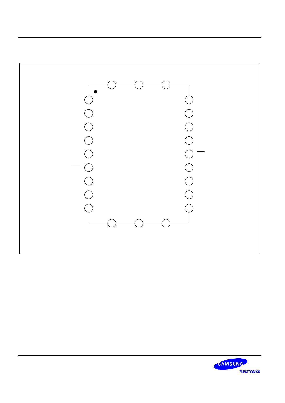
S1M8831A/33 FRACTIONAL-N RF/INTEGER-N IF DUAL PLL
PIN CONFIGURATION
OUT0 OUT1 VDDIF
24 23 22
VPRF
CPORF
DGND
finRF
finRF
GND
RF
OSCx
OSCin
1VDDRF
2
3
4
5
S1M8831A/33
6
7
8
9
21
20
19
18
17
16
15
14
13
VPIF
CPOIF
DGND
finIF
finIF
GND
IF
LE
DATA
CLCOK
10 11 12
foLD RF_EN IF_EN
24-QFN
4

FRACTIONAL-N RF/INTEGER-N IF DUAL PLL S1M8831A/33
PIN DESCRIPTION
Pin No. Symbol I/O Description
1
VDDRF
–
RF PLL power supply(2.7V to 4.0V). Must be equal to VDDIF.
2
3
VPRF
CPoRF
–
Power supply for RF charge pump. Must be ≥ VDDRF and VDDIF.
O RF charge pump output. Connected to an external loop filter.
4 DGND – Ground for RF PLL digital circuitry.
5
6
finRF
finRF
I RF prescaler input. Small signal input from the external VCO.
I RF prescaler complementary input. For a single-ended output RF VCO, a
bypass capacitor should be placed as close as possible to this pin and be
connected directly to the ground plane.
7
GND
RF
– Ground for RF PLL analog circuitry.
8 OSCx I RF R counter input (IF_N[22]=0) or not-use (IF_N[22]=1) which can be
configured depending on the state of the program bit IF_N[22].
9 OSCin I Oscillator input to drive both the IF and RF R counter inputs (IF_N[22]=1) or
only the IF R counter (IF_N[22]=0) which can be configured depending on
the state of the program bit IF_N[22].
10 foLD O Multiplexed output of N or R divider and RF/IF lock detect.
11 RF_EN I RF PLL Enable (enable when high, power down when low).
Controls the RF PLL to power down directly, not depending on a program
control. Also sets the charge pump output to be in TRI-STATE when LOW.
Powers up when HIGH depends on the state of RF_CTL_WORD.
12 IF_EN I IF PLL Enable(enable when high, power-down when low).
Controls the IF PLL to power down directly. The same as RF_EN except
that power-up depends on the state of IF_CTL_WORD.
13 CLOCK I CMOS clock input. Data for the various counters is clocked into the 24-bit
shift register on the rising edge.
14 DATA I Binary serial data input. Data entered MSB (Most Significant Bit) first.
15 LE I Load enable when LE goes HIGH. High impedance CMOS input.
16
17
GND
finIF
IF
– Ground for IF analog circuitry.
I IF Prescaler complementary input. For a single-ended output IF VCO, a
bypass capacitor should be placed as close as possible to this pin.
18
finIF
I IF prescaler input. Small signal input from the VCO.
19 DGND – Ground for IF PLL digital circuitry.
20 CPoIF O IF charge pump output. Connected to an external loop filter.
5

S1M8831A/33 FRACTIONAL-N RF/INTEGER-N IF DUAL PLL
PIN DESCRIPTION (Continued)
Pin No. Pin Name I/O Descriptions
21
VPIF
–
Power supply for IF charge pump. Must be ≥ VDDRF and VDDIF.
22
23 OUT1 O Programmable CMOS output. Level of the output is controlled by
24 OUT0 O Programmable CMOS output. Level of the output is controlled by
VDDIF
–
IF PLL power supply (2.7V to 4.0V). Must be equal to VDDRF.
RF_N[19] bit.
RF_N[18] bit. In the speedy lock mode, the OUT0 and OUT1 pins can be
utilized as synchronous switches between active low and tri-state.
6
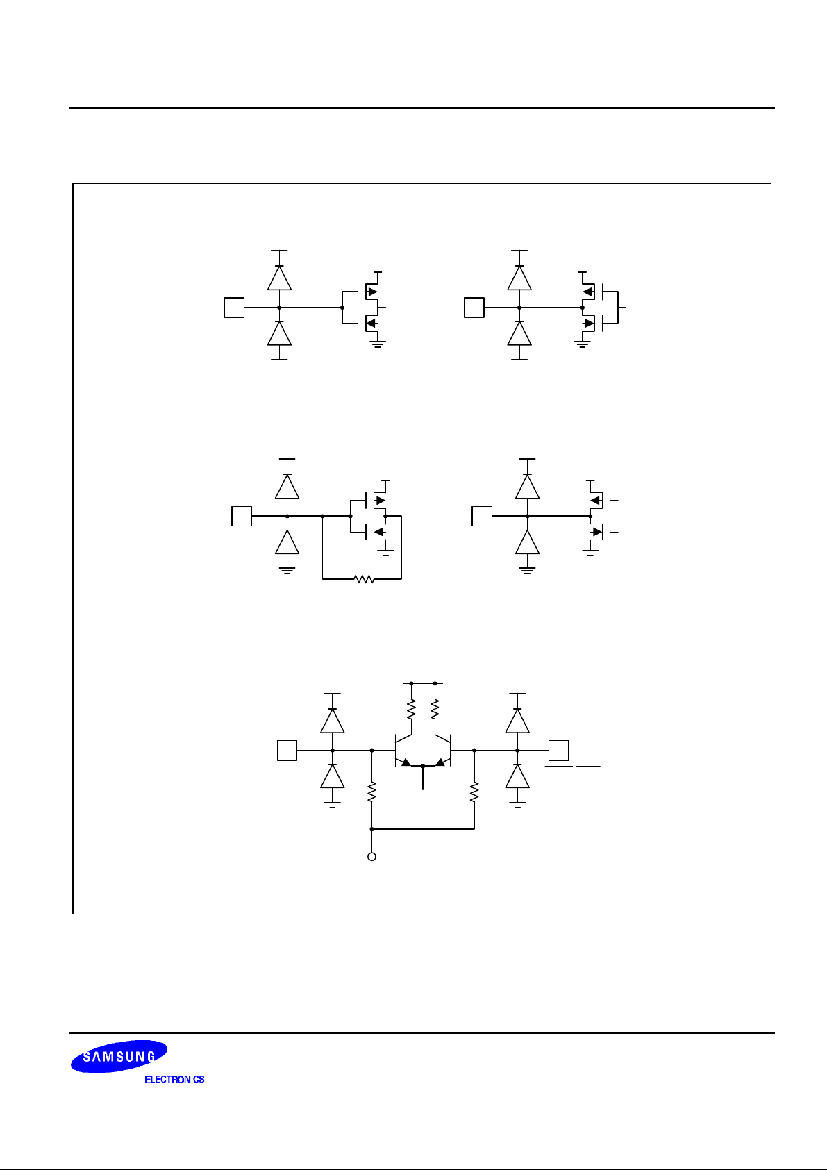
FRACTIONAL-N RF/INTEGER-N IF DUAL PLL S1M8831A/33
EQUIVALENT CIRCUIT DIAGRAM
CLOCK, DATA, LE foLD
OSCin, OSCx CPORF, CPOIF
finRF, finIF
finRF, finRF, finIF, finIF
V
bias
finRF, finIF
7
S1M8831A/33 FRACTIONAL-N RF/INTEGER-N IF DUAL PLL
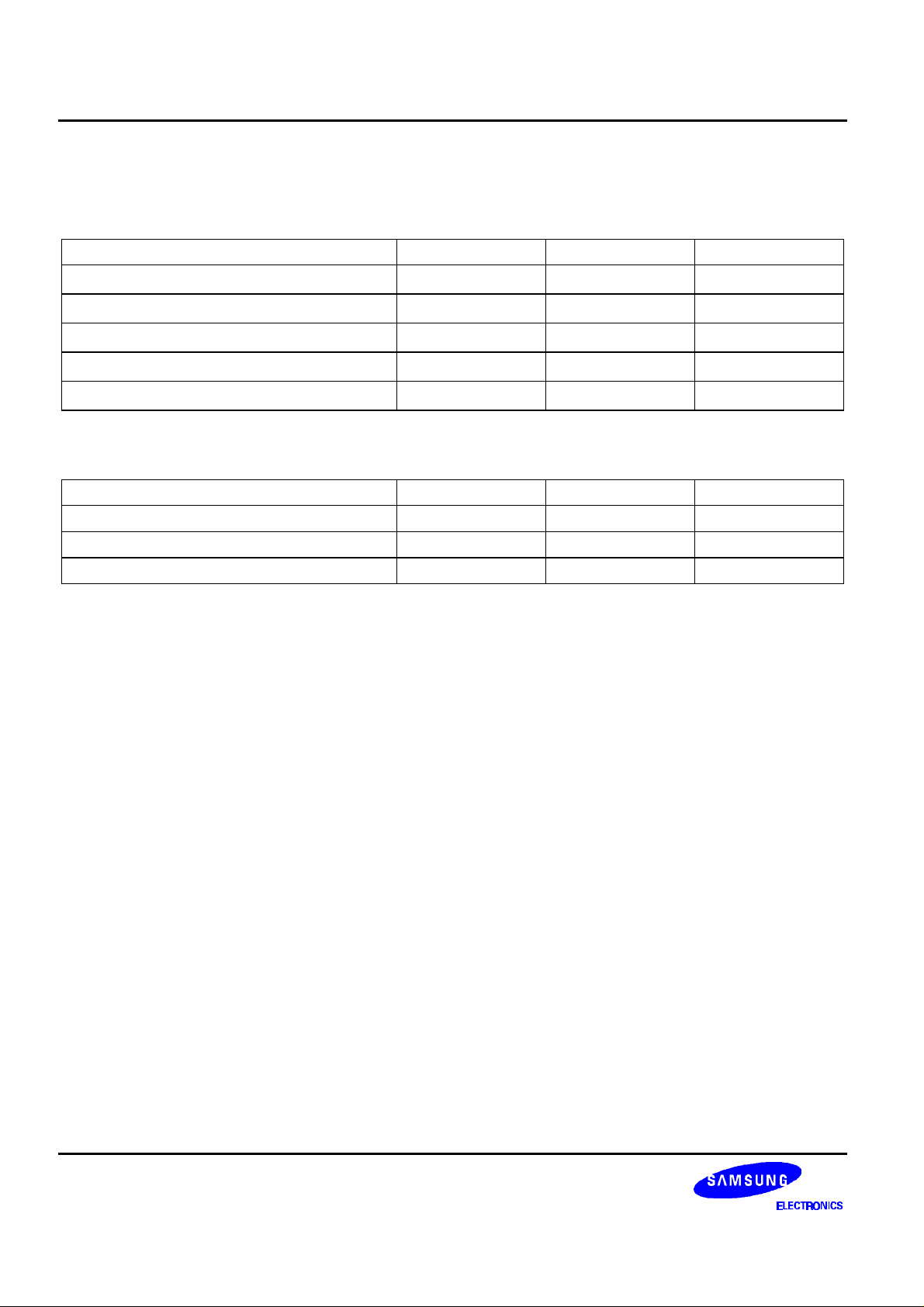
ELECTRICAL SPECIFICATIONS
ABSOLUTE MAXIMUM RATINGS
Characteristics Symbol Value Unit
Power supply voltage
Voltage on any pin with GND = 0 volts
Power dissipation
Operating temperature
Storage temperature
ELECTROSTATIC CHARACTERISTICS
Characteristics Pin No. ESD Level Unit
Human body model All
Machine model All
Charge device model All
V
T
DD
V
P
D
T
STG
0.0 to 4.0 V
I
-0.3 to VDD + 0.3
V
600 mW
a
-40 to +85
-65 to +150
< ± 2000
< ± 300
< ± 800
°C
°C
V
V
V
NOTE: These devices are ESD sensitive. These devices must be handled in an ESD protected environment.
8
FRACTIONAL-N RF/INTEGER-N IF DUAL PLL S1M8831A/33
ELECTRICAL CHARACTERISTICS
(V
= 3.0V, VP = 3.0V, Ta = 25°C, unless otherwise specified.)
DD
Characteristic Symbol Test Conditions Min. Typ. Max. Unit
Power supply voltage
Power supply current S1M8831A
RF+IF
S1M8833
V
DD
V
P
I
DD
Fractional-N mode
(f
= 19.68MHz,
osc
2.7 3.0 4.0 V
V
DD
3.0 4.0
5.0 mA
RF R = 2) 7.0
RF+IF
S1M8831A
Quiescent State 3.5
RF+IF
S1M8833
5.5
RF+IF
IF only 1.5
Power down current
I
PWDN
V
DD
= 3.0V
1 10
µA
Digital Inputs: CLOCK, DATA and LE
High level input voltage
Low level input voltage
High level input current
Low level input current
V
IH
V
IL
I
IH
I
IL
V
= 2.7V to 4.0V
DD
V
= 2.7V to 4.0V
DD
V
= V
IH
DD
V
= 0V, V
IL
= 4.0V
= 4.0V
DD
0.7V
DD
0.3V
-1.0 +1.0
-1.0 +1.0
DD
V
V
µA
µA
Reference Oscillator Input: OSCin
Input current
I
IHR
I
ILR
V
IH
V
IL
= V
DD
= 0V, V
= 4.0V
= 4.0V
DD
-100
+100
µA
µA
Digital Output: foLD
High level output voltage
Low level output voltage
V
OH
V
OL
I
= -500µA
out
I
= +500µA
out
VDD-0.4
V
0.4 V
9

S1M8831A/33 FRACTIONAL-N RF/INTEGER-N IF DUAL PLL
ELECTRICAL CHARACTERISTICS (Continued)
(V
= 3.0V, VP = 3.0V, Ta = 25°C, unless otherwise specified.)
DD
Characteristic Symbol Test Conditions Min. Typ. Max. Unit
Operating Frequency, Input Sensitivity (Programmable Divider, PFD)
RF operating
frequency
S1M8833
finRF
Fractional-N mode
(f
= 19.68MHz,
osc
1.6 1.65 GHz
RF R = 2)
S1M8831A Fractional-N mode
(f
= 19.68MHz,
osc
0.71 1.2 GHz
RF R = 2)
IF operating frequency
Reference oscillator input
finIF V
OSC
in
DD
= 3.0
45 520 MHz
2 40 MHz
frequency
Phase detector operating
f
PD
10 MHz
frequency
P
RF input sensitivity
IF input sensitivity
Reference oscillator input
RF VDD = 3.0V
fin
V
DD
P
IF V
V
OSCin
fin
DD
= 4.0V
= 2.7V to 4.0V
-15 0 dBm
-10 0 dBm
-10 0 dBm
0.5
V
DD
V
PP
sensitivity
Charge Pump Outputs: CPoRF, CPoIF
RF charge pump output current
IF charge pump output current
I
CPRF-
SOURCE_min
I
CPRF-
SIINK_min
I
CPRF-
SOURCE_
max
I
CPRF-
SIINK_max
I
CPRF-
SOURCE_min
I
CPRF-
SIINK_min
I
CPRF-
SOURCE_max
I
CPRF-
SIINK_max
VCP = VP/2,
RF_CP_WORD=0000
V
= VP/2,
CP
RF_CP_WORD=0000
V
= VP/2,
CP
RF_CP_WORD=1111
V
= VP/2,
CP
RF_CP_WORD=1111
V
= VP/2,
CP
CP_GAIN_8=0
V
= VP/2,
CP
CP_GAIN_8=0
V
= VP/2,
CP
CP_GAIN_8=1
V
= VP/2,
CP
CP_GAIN_8=1
-50 uA
+50 uA
-800 uA
+800 uA
-100 uA
+100 uA
-800 uA
+800 uA
10
 Loading...