

查询KB2511B供应商
DEFLECTION PROCESSOR FOR MULTISYNC MONITORS S1D2511B01
DEFLECTION PROCESSOR
32-SDIP-400
The S1D2511B01 is a monolithc integrated circuit
assembled in 32 pins shrunk dual in line plastic package. This IC controls all the functions related to the horizontal and vertical deflection in multimodes or multifrequency computer display monitors.
The internal sync processor, combined with the very
powerful geometry correction block make the S1D2511B
suitable for very high performance monitors with very
few external components. The horizontal jitter level is
very low. It is particularly well suited for high-end 15”
and 17” monitors.
FUNCTIONS
ORDERING INFORMATION
• Defiection Processor
• I2C BUS Control
• B+ Regulator
• Vertical Parabola Generator
• Horizontal and Vertical dynamic focus
S1D2511B01-A0B0 32-SDIP 0 °C — 70 °C
FEATURES
(HORIZONTAL)
• Self-adaptative
• Dual PLL concept
• 150kHz maximum frequency
• X-RAY protection input
• I2C controls : Horizontal duty-cycle, H-position,free running
frequency, frequency generator for burn-in mode.
(VERTICAL)
• Vertical ramp generator
• 50 to 165Hz AGC loop
• Geometry tracking with V-POS & AMP
• I2C Controls :
V-AMP, V-POS, S-CORR, C-CORR
(I2C GEOMETRY CORRECTIONS)
• Vertical parabola generator
(Pincushion-E/W, Keystone)
Device Package Operating Temperature
• Horizontal Dynamic Phase
(Side Pin balance & parallelogram)
• Horizontal and vertical dynamic focus
(Horizontal Focus Amplitude, Horizontal
Focus Symmetry, Vertical Focus Amplitude)
(GENERAL)
• Sync Processor
• 12V supply voltage
• Hor. & Vert, lock/unlock outputs
• Read/Write I2C interface
• Vertical moire
• B+ Regulator
-Internal PWM generator for B+ current mode
step-up converter.
- Switchable to step-down converter
- I2C adjustable B+ reference voltage
- Output pulses synchronized on horizontal
frequency
- Internal maximum current limitation.
1
S1D2511B01 DEFLECTION PROCESSOR FOR MULTISYNC MONITORS
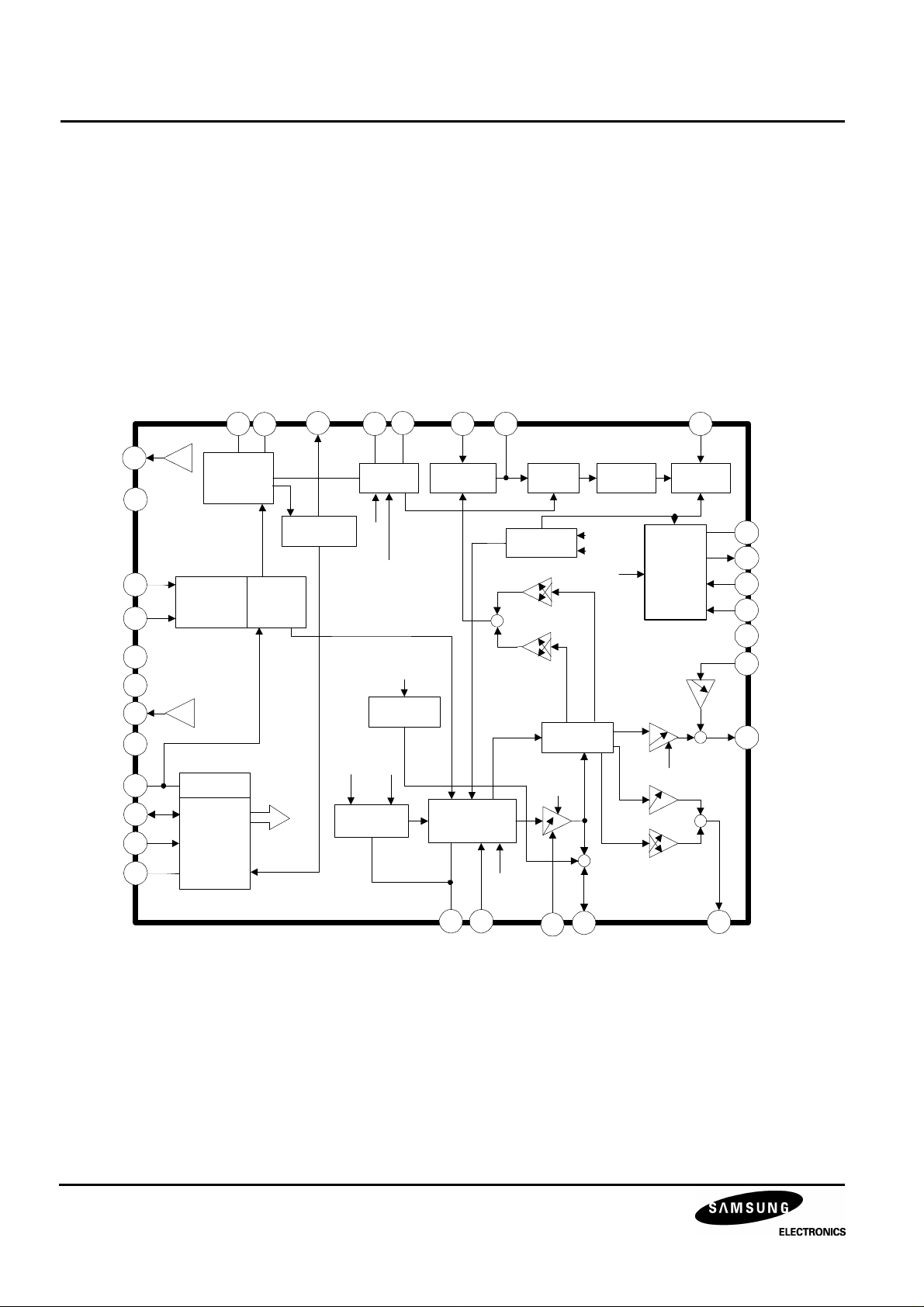
BLOCK DIAGRAM
HREF
HGND
H/HVIN
VSYNC
IN
VCC
XRAY
VREF
VGND
5V
SDA
SCL
GND
PLL1F
H POSITION
7
8
13
VREF
11
1
2
FREQUENCY
COMPARATOR
H-PHASE(7 bits)
SYNC INPUT
SELECT
(1bit)
PHASE/
SYNC
PROCESSOR
HLOCKOUT
3
LOCK/UNLOCK
IDENTIFICATION
R0
C0
5
6 12 4
PHASE
COMPARATOR
Forced
Freq.
2 bits
VCO
Free running
5 bits
29
25
VSYNC
MOIRE
21
REF
V
CANCEL
5 BITS+ON/OFF
19
32
RESET
GENERATOR
31
2
30
I C INTERFACE
6 bits 8 bits
S AND C
CORRECTION
VERTICAL
OSCILLATOR
RAMP GENERATOR
27
HFLY
+
VPOS
7bits
PLL2C
PHASE
SHIFTER
SAFETY
PROCESSOR
2
X
Spin Bal
6 bits
2
X
Key Bal
6 bits
GEOMETRY
TRACKING
VAMP
7 bits
Vcc
XRAY
B+ ADJUST
7 bits
+
H-DUTY
(5 bits)
Amp & symmetry
2x5 bits
keyst
6 bits
BUFFER
B+
CONTROLLER
VAMP
6 bits
PCC
7 bits
2
X
X
26
HOUT
X
HOUT
2
+
+
14
28
15
16
17
9
10
COMP
B+ OUT
REGIN
ISENSE
BGND
HFOCUS
CAP
FOCUS
2
22 20
VCAP
VACCAP
18
BREATH
23
VOUT
24
EWOUT

DEFLECTION PROCESSOR FOR MULTISYNC MONITORS S1D2511B01
PIN CONFIGURATIONS
1
2
3
4
5
6
7
8
9
10
11
H/HVIN
VSYNCIN
HLOCKOUT
PLL2C
C0
R0
PLL1F
HPOSITION
HFOCUSCAP
FOCUSOUT
HGND
BOUT
HOUT
XRAY
EWOUT
S1D2511B
VOUT
VCAP
5V
SDA
SCL
VCC
GND
32
31
30
29
28
27
26
25
24
23
22
12
13
14
15
16
HFLY
HREF
COMP
REGIN
ISENSE
VREF
VAGCCAP
VGND
BREATH
B+GND
21
20
19
18
17
3
S1D2511B01 DEFLECTION PROCESSOR FOR MULTISYNC MONITORS
PIN DESCRIPTION
Table 1. Pin Description
No Pin Name Description
1 H/HVIN TTL compatible horizontal sync input(Separate or composite)
2 VSYNCIN TTL compatible vertical sync input (for separated H&V)
3 HLOCKOUT First PLL lock/unlock output (0V unlocked - 5V locked)
4 PLL2C Second PLL loop filter
5 C0 Horizontal oscillator capacitor
6 R0 Horizontal oscillator resistor
7 PLL1F First PLL loop filter
8 HPOSITION Horizontal position filter(Capacitor to be connected to HGND)
9 HFOCUSCAP Horizontal dynamic focus oscillator capacitor
10 FOCUSOUT Mixed horizontal and vertical dynamic focus output
11 HGND Horizontal Section Ground
12 HFLY Horizontal Flyback Input (positive polarity)
13 HREF Horizontal Section Reference Voltage (to be filtered)
14 COMP B+ error amplifier output for frequency compensation and gain setting
15 REGIN Regulation input of B+ control loop
16 ISENSE Sensing of external B+ switching transistor current or switch for step-down converter
17 B+GND Ground (related to B+ reference adjustment)
18 BREATH DC breathing input control(Compensation of vertical amplitude against EHV variation)
19 VGND Vertical section ground
20 VAGCCAP Memory capacitor for automatic gain control loop in vertical ramp generator
21 VREF Vertical section reference voltage (to be filtered)
22 VCAP Vertical sawtooth generator capacitor
23 VOUT Vertical ramp output (with frequency independant amplitude and S or C corrections if any).
It is mixed with vertical position voltage and vertical moire.
24 EWOUT Pincushion-East/West correction parabola output
25 XRAY X-RAY protection input (with internal latch function)
26 HOUT Horizontal drive output (internal transistor, open collector)
27 GND General ground (referenced to Vcc)
28 BOUT B+ PWM regulator output
29 Vcc Supply voltage (12V typ)
30 SCL
31 SDA
32 5V Supply voltage (5V typ)
I2C clock input
I2C data input
4
DEFLECTION PROCESSOR FOR MULTISYNC MONITORS S1D2511B01
REFERENCE DATA
Table 2. Reference Data
Parameter Value Unit
Horizontal frequency 15 to 150 kHz
Autosynch frequency (for given R0 and C0) 1 to 4.5FO FH
± Horizontal sync polarity input YES
Polarity detection (on both horizontal and vertical section) YES
TTL Composite synch YES
Lock/Unlock identification (on both horizontal 1st PLL and vertical section) YES
I2C control for H-Position
XRay protection YES
I2C horizontal duty cycle adjust
I2C free running frequency adjustment
Stand-by function YES
Dual polarity H-Drive outputs NO
Supply voltage monitoring YES
PLL1 inhibition possibility NO
Blanking output NO
Vertical frequency 35 to 200 Hz
Vertical autosync (for 150nF on Pin22 and 470nF on Pin20) 50 to 165 Hz
Vertical S-Correction YES
Vertical C-Correction YES
Vertical amplitude adjustment YES
DC breathing control on Vertical amplitude YES
±10 %
30 to 60 %
0.8 to 1.3FO FH
East/West parabola output(also known as Pin cushion output) YES
East/West correction amplitude adjustment YES
Keystone adjustment YES
Internal dynamic horizontal phase control YES
Side pin balance amplitude adjustment YES
Parallelogram adjustment YES
Tracking of geometric corrections with vertical amplitude and position YES
5
S1D2511B01 DEFLECTION PROCESSOR FOR MULTISYNC MONITORS
Table 2. Reference Data (Continued)
Parameter Value Unit
Reference voltage (both on horizontal and vertical) YES
Dynamic focus (both on horizontal and vertical) YES
I2C horizontal dynamic focus amplitude adjustment
I2C horizontal dynamic focus symmetry adjustment
I2C vertical dynamic focus amplitude adjustment
Deflection of input Sync type(biased from 5V alone) YES
Vertical moire output YES
I2C controlled V-moire amplitude
Frequency generator for burn-in YES
Fast I2C read/write
B+ regulation adjustable by I2C
YES
YES
YES
YES
400 kHz
YES
6
DEFLECTION PROCESSOR FOR MULTISYNC MONITORS S1D2511B01
ABSOLUTE MAXIMUM RATINGS
No Item Symbol Value Unit
1 Supply voltage (pin 29) V
2 Supply voltage (pin 32) V
3 Maximum voltage on Pin 4
Pin 9
Pin 5
Pins 6,7,8,14,15,16,20,22
Pins 10,18,23,24,25,26,28
Pins 1,2,3,30,31
4 ESD susceptibillty
VESD 2
CC
DD
V
IN
13.5 V
5.7 V
4.0
5.5
6.4
8.0
V
CC
V
DD
Human body model, 100pF discharge through
1.5KΩ
300
EIAJ norm, 200pF discharge through 0Ω
5 Storage temperature Tstg - 40, +150 °C
6 Operating temperature Topr 0, +70 °C
THERMAL CHARACTERISTICS
No Item Symbol Value Unit
1 Junction temperature Tj +150 °C
V
V
V
kV
V
2 Junction-ambient thermal resistance θja 65 °C/W
SYNC PROCESSOR
OPERATING CODNITIONS
Table 3. Sync Processor Operating Codnitions
Parameter Symbol Conditions Min Typ Max Unit
Horizontal sync input voltage HsVR Pin 1 0 5 V
Minimum horizontal input pulse duration MinD Pin 1 0.7 µs
Maximum horizontal input signal duty cycle Mduty Pin 1 25 %
Vertical sync input voltage VsVR Pin 2 0 5 V
Minimum vertical sync pulse width VSW Pin 2 5 µs
Maximum vertical sync input duty cycle VSmD Pin 2 15 %
Maximum vertical sync width on TTL H/V composite VextM Pin 1 750 µs
Sink and source current
I
HLOCKOUT
Pin 3 250 µA
7
S1D2511B01
ELECTRICAL CHARACTERISTICS
( V = 5V, Tamb = 25 °
Table 4. Sync Processor Electrical Characteristics
Symbol Conditions Typ Max
Horizontal and vertical input threshold
voltage (pin 1, 2)
Low level
High level
0.8 V
Horizontal and vertical pull-up resister RIN 200 K
Falling and rising output CMOS buffer TfrOut 200 ns
(pin 3)
TH
2
I
(9)
(See also I
VHlock
VoutT C0 = 820pF 35 %
2 2
LOCKOUT
= -250 A
Unlocked, I = +250µ
C sub address control)
0
5
2
C Read/Write Operating Conditions
Symbol Min Max Unit
VinH 3.0 5.0 V
VinL 0 1.5 V
fSCL - 200 kHz
V
V
8
tBUF 1.3 - uS
tHDS 0.6 - uS
tSUP 0.6 - uS
tLOW 1.3 - uS
tHIGH 0.6 - uS
tHDAT 0.3 - uS
tSUPDAT 0.25 - uS
tR - 1.0 uS
tF - 3.0 uS
DEFLECTION PROCESSOR FOR MULTISYNC MONITORS S1D2511B01
I2C BUS Timing Requirement
Stop:Clock High
SDA
SCL
tBUF
Start:Clock High
tHDS
tLOW
tSUPDAT
tHDAT
tSUP
tHIGH
Data Change:Clock Low
ELECTRICAL CHARACTERISTICS
( VDD = 5V, Tamb = 25 °C)
Table 6. I2C Read/Write Electrical Characteristics
Parameter Symbol Conditions Min Typ Max Unit
I2C PROCESSOR
Maximum clock frequency Fscl Pin 30 400 kHz
Low period of the SCL clock Tlow Pin 30 1.3 µs
High period of the SCL clock Thigh Pin 30 0.6 µs
SDA and SCL input threshold Vinth Pin 30, 31 2.2 V
Acknowledge output voltage on SDA input with
3mA
VACK Pin 31 0.4 V
HORIZONTAL SECTION
OPERATING CONDITIONS
Table 7. Horizontal Section Operating Conditions
Parameter Symbol Conditions Min Typ Max Unit
VCO
Minimum oscillator resistor R
Minimum oscillator capacitor C
Maximum oscillator frequency F
0(Min.)
0(Min.)
(Max.)
OUTPUT SECTION
Maximum input peak current I12m Pin 12 5 mA
Horizontal drive output maximum
current
HOI Pin26, sunk current 30 mA
Pin 6 6 KΩ
Pin 5 390 pF
150 kHz
9
S1D2511B01 DEFLECTION PROCESSOR FOR MULTISYNC MONITORS
ELECTRICAL CHARACTERISTICS
( VDD = 5V, Tamb = 25 °C)
Table 8. Horizontal Section Electrical Characteristics
Parameter Symbol Conditions Min Typ Max Unit
SUPPLY AND REFERENCE VOLTAGE
Supply voltage Vcc Pin 29 10.8 12 13.2 V
Supply voltage V
Supply current I
Supply current I
Horizontal reference voltage V
Vertical reference voltage V
Max. sourced current on V
Max. sourced current on V
REF-H
REF-V
I
I
DD
CC
DD
REF-H
REF-V
REF-H
REF-V
Pin 32 4.5 5 5.5 V
Pin 29 50 mA
Pin 32 5 mA
Pin 13, I=-2mA 7.4 8 8.6 V
Pin 21, I=-2mA 7.4 8 8.6 V
Pin 13 5 mA
Pin 21 5 mA
1st PLL SECTION
Polarity integration delay HpoIT Pin 1 0.75 ms
VCO control voltage (pin 7) V
VCO gain (pin 7 ) V
Horizontal phase adjustment
Horizontal phase setting value(Pin 8)
(11)
(11)
Minimum current value
Typical value
Maximum value
VCO
COG
Hph % of horizontal period ± 10 %
Hphmin
Hphtyp
Hphmax
PLL1 filter current charge IPII1U
IPII1L
Free running frequency fo R0=6.49KΩ,C0=820pF,
Free running frequency thermal drift
(no drift on external components)
(7)
dF0/dT -150 ppm/c
Free running frequency adjustment
Minimum value
Maximum value
f0(Min.)
f0(Max.)
V
=8V
REF-H
f0
fH (Max.)
R0=6.49KΩ, C0=820pF,
dF/dV=1/11R0C
0
Sub-address 01
Byte x 1111111
Byte x 1000000
Byte x 0000000
PLL1 is unlocked
PLL1 is locked
f0=0.97/8R0C
0
Sub-address 02
Byte x x x 11111
Byte x x x 00000
1.3
6.2
17 kHz/V
2.6
3.2
3.8
±140
±1
±140
±1
0.8
1.3
PLL1 capture range CR R0=6.49KΩ,C0=820pF,
from f0+0.5KHz to 4.5Fo
23.5 KHz
Safe forced frequency
SF1 Byte 11 x x x x x x
SF2 Byte 10 x x x x x x
fH(Min.)
fH(Max.)
SFF Sub-address 02
100
2F0
3F0
2ND PLL SECTION HORIZONTAL OUTPUT SECTION
V
V
V
V
V
µA
mA
µA
mA
F0
F0
KHz
10
DEFLECTION PROCESSOR FOR MULTISYNC MONITORS S1D2511B01
Table 8. Horizontal Section Electrical Characteristics (Continued)
Parameter Symbol Conditions Min Typ Max Unit
Flyback input threshold
voltage (pin12)
Horizontal jitter Hjit 70 ppm
Horizontal drive output duty-cycle
(pin 26)
(1, 2)
Low level
High level
X-RAY protection input threshold
voltage
Internal clamping levels on 2nd PLL loop
filter (pin 4 )
Threshold voltage to stop H-out, V-out
when VCC < VSCinh
Horizontal drive output (low level) HDvd Pin 26 I
HORIZONTAL DYNAMIC FOCUS FUNCTION
Horizontal dynamic focus sawtooth
Minimum level
Maximum level
Horizontal dynamic focus sawtooth
Discharge width
Bottom DC output level HDFDC R
DC output voltage thermal drift TDHDF 200 ppm/C
Horizontal dynamic focus amplitude
Min Byte xxx11111
Typ Byte xxx10000
Max Byte xxx00000
Horizontal dynamic focus keystone
Min A/B Byte xxx11111
Typ Byte xxx10000
Max Byte xxx00000
VERTICAL DYNAMIC FOCUS FUNCTION (POSITIVE PARABOLA)
Vertical dynamic focus parabola (added to
horizontal one) amplitude with VOUT and
VPOS typical
Min. Byte 000000
Typ. Byte 100000
Max. Byte 111111
Parabola amplitude function of VAMP
(tracking between VAMP and VDF) with
VPOS typ. (see figure 1)
Parabola assymetry function of VPOS
control (tracking between VPOS and VDF)
with VAMP Max.
(3)
FBth 0.65 0.75 V
Sub-address 00
HDmin
HDmax
XRAYth
Vphi2 Low level
Byte xxx11111
Byte xxx00000
(12)
Pin 25
High level
(2)
30
60
8 V
1.6
3.7
%
%
VSCinh Pin 29 7.5 V
=30mA 0.4 V
OUT
HDFst Capacitor on HfocusCap
and C0=820pF,
TH=20µS, Pin 9
2
4.7
HDFdis Start by Hfly center 400 ns
=10KΩ, pin 10 2 V
LOAD
HDFamp Sub-address 03, pin 10,
FH=50kHz, Keystone
Typ
1
1.5
3
Vpp
Vpp
Vpp
HDFkeyst Sub-address 04,
FH = 50kHz, Typ amp
B/A
A/B
A/B
2.2
2.2
3.5
1.0
3.5
AMPVDF Sub-address 0F
0
0.5
1
Vpp
Vpp
Vpp
VDFAMP Sub-address 05
Byte 10000000
Byte 11000000
Byte 11111111
0.6
1
1.5
Vpp
Vpp
Vpp
VHDFKeyt Sub-address 06
Byte x0000000
Byte x1111111
0.52
0.52
Vpp
Vpp
V
V
V
V
11

S1D2511B01 DEFLECTION PROCESSOR FOR MULTISYNC MONITORS
VERTICAL SECTION
OPERATING CONDITIONS
Table 9. Vertical Section Operating Conditions
Parameter Symbol Conditions Min Typ Max Unit
OUTPUTS SECTION
Maximum EW output voltage VEWM Pin 24 6.5 V
Minimum EW output voltage VEWm Pin 24 1.8 V
Minimum load for less than 1% vertical amplitude drift R
LOAD
Pin 20 65 MΩ
ELECTRICAL CHARACTERISTICS
(VCC = 12V, Tamb = 25 °C)
Table 10. Vertical Section Electrical Characteristics
Parameter Symbol Conditions Min Typ Max Unit
VERTICAL RAMP SECTION
Voltage at ramp bottom point VRB V
Voltage at ramp top point (with sync) V
REF-V
VRT V
Voltage at ramp top point (without sync) VRTF Pin 22
Vertical sawtooth discharge time duration (pin 22) VSTD With 150nF cap 70 µs
Vertical free running frequency
(4, 5)
see
AUTO -SYNC frequency
(13)
Ramp amplitude drift versus frequency at
VFRF C
ASFR C22=150nF ± 5%
RAFD C22=150nF
Maximum vertical amplitude
Ramp linearity on pin 22 (∆I22/I22)
(4, 5)
see
RIin V20=4.3v,
=8V, pin 22 2 V
REF-V
=8V, Pin 22 5 V
REF-V
VRT-01
OSC(pin22)
=150nF
100 Hz
measured on pin 22
50 165 Hz
(6)
See
200 TBD ppm/
50Hz<f and f<165Hz
0.5 %
2.5<V27 &
V27<4.5V
V
Hz
Vertical position adjustment voltage
(pin 23 - VOUT centering)
Vertical output voltage
(peak-to-peak on pin 23 )
Vpos Sub address 06
Byte x0000000
Byte x1000000
Byte x1111111 3.65
VOR Sub address 05
Byte x0000000
Byte x1000000
Byte x1111111 3.5
3.2
3.5
3.8
2.25
3
3.75
3.3 V
2.5 V
Vertical output Maximum current(Pin 23) VOI ±5 mA
Max vertical S-correction amplitude
XOXXXXXX inhibits S-CORR
X1111111 gives max S-CORR
(14)
dVS Sub address 07
∆V/Vpp at TV/4
∆V/Vpp at 3TV/4
-4
+4
12
V
V
V
V
%
%

DEFLECTION PROCESSOR FOR MULTISYNC MONITORS S1D2511B01
Table 10. Vertical Section Electrical Characteristics (Continued)
Parameter Symbol Conditions Min Typ Max Unit
Vertical C-Corr amplitude
Ccorr Sub address 08
XOXXXXXX inhibits C-corr
EAST/WEST FUNCTION
DC output voltage with typ Vpos, keystone,
corner and corner balance inhibited
DC output voltage thermal drift TDEW
Parabola amplitude with Vamp Max.
V-Pos typ, keystone ilhibited
Parabola amplitude function of V-AMP control
(tracking between V-AMP and E/W) with typ Vpos
ketstone, EW Typ amplitude
(8)
Keystone adjustment capability with typ Vpos,
EW
DC
EWpara Sub address 0A
EWtrack Sub address 05
KeyAdj
EW typ amplitude and vertical amplitude max,
(8)
A/B Ratio(see figure 2)
B/A Ratio
∆V/Vpp at TV/2
Byte X1000000
Byte X1100000
Byte X1111111
pin 24,
see figure 2
see note 7 100 ppm/
DC
Byte 1111111
Byte 1010000
Byte 1000000
Byte 1000000
Byte 1100000
Byte 1111111
Sub address 09
Byte 1x000000
Byte 1x111111
-3
0
3
2.5 V
2.5
1.25
0
0.45
0.8
1.25
1
1
%
%
%
C
V
V
V
V
V
V
Vpp
Vpp
Intrinsic keystone function of V-POS control
(tracking between V-pos and EW) Max amplitude
and vertical amplitude max.
(10)
A/B Ratio
B/A Ratio
KeyTrack
Sub address 09
Byte x0000000
Byte x1111111
INTERNAL HORIZONTAL DYNAMIC PHASE CONTROL FUNCTION
Side pin balance parabola amplitude (figure3) with
Vamp max, V-POS typ and parallelogram inhibited
(8,9)
Side pin balance parabola amplitude function of
Vamp control (tracking between Vamp and SPB)
with SPB max, V-POS typ and parallelogram
inhibited
(8,9)
Parallelogram adjustment capability with Vamp
max, V-POS typ and SPB max
(8,9)
A/B Ratio
B/A Ratio
Intrinsic parallelogram function of Vpos control
(tracking between V-pos and DHPC) with Vamp
max, SPB max and parallelogram inhibited
(8, 9)
A/B Ratio
B/A Ratio
SPBpara Sub address 0D
Byte x1111111
Byte x0000000
SPBtrack Sub address 05
Byte 10000000
Byte 11000000
Byte 11111111
ParAdj Sub address 0E
Byte x1111111
Byte x1000000
Partrack Sub address 06
Byte x0000000
Byte x1111111
0.52
0.52
+1.4
-1.4
0.5
0.9
1.4
+1.4
-1.4
0.52
0.52
%TH
%TH
%TH
%TH
%TH
%TH
%TH
13

S1D2511B01 DEFLECTION PROCESSOR FOR MULTISYNC MONITORS
Table 10. Vertical Section Electrical Characteristics (Continued)
Parameter Symbol Conditions Min Typ Max Unit
VERTICAL MOIRE
Vertical moire (measured on VOUTDC) pin 23 VMOIRE Sub address 0C
Byte 01x11111 6 mV
BREATHING COMPENSATION
DC breathing control range
(15)
BRRANG V18 1 12 V
Vertical output variation versus DC breathing control (Pin 23)
BRADj V18≥V
V18=4V
REF-V
0
-10
B+ SECTION
OPERATING CONDITIONS
Table 11. B+ Section Operating Conditions
Parameter Symbol Conditions Min Typ Max Unit
Minimum feedback resistor FeedRes Resistor between pins 15 and 14 5 KΩ
ELECTRICAL CHARACTERISTICS
(VCC = 12V, Tamp = 25 °C )
Table 12. B+ Section Electrical Characteristics
Parameter Symbol Conditions Min Typ Max Unit
Error amplifier open loop gain OLG
Unity gain band width UGBW
At low frequency
(7)
see
(10)
85 dB
6 MHz
%
%
Regulation input bias current IRI Current sourced by pin 15
(PNP base)
Maximum guaranted error amplifier
output current
Current sense input voltage gain CSG Pin 16 3
Max current sense input thres hold
voltage
Current sense input bias current ISI Current sunk by pin 16
Maxmum external power transistor on
time
B+ output low level saturation voltage B+OSV V28 with I28=10mA 0.25 V
Internal reference voltage IV
EAOI Current sourced by pin 14
Current sunk by pin 14
MCEth Pin 16 1.2 V
(NPN base )
Tonmax % of H-period
@ f0=27kHz
REF
On error amp
(+) input for subaddress 0B
byte 1000000
(16)
0.2 µA
0.5
2
1 µA
100 %
4.8 V
14
mA
mA

DEFLECTION PROCESSOR FOR MULTISYNC MONITORS S1D2511B01
Table 12. B+ Section Electrical Characteristics
Internal reference voltage adjustment
range
Threshold for step-up/step-down selection
Falling time t
V
REFADJ
DWMSEL Pin 16 6 V
FB+
Byte 111111
Byte 000000
Pin 28 100 ns
+20
-20
%
%
15

S1D2511B01 DEFLECTION PROCESSOR FOR MULTISYNC MONITORS
NOTES;
1.Duty cycle is the ratio of power transistor OFF time period. Power transistor is OFF when output transistor is
OFF.
2.Initial condition for safe operation start up.
3.S and C correction are inhibited so the output sawtooth has a linear shape.
4.With register 07 at byte x0xxxxxx (s-correction control is inhibited) then the S correction is inhibited, consequently
the sawtooth has a linear shape.
5.With register 08 at byte x0xxxxxx (C-Correction control is inhibited) then the C correction is inhibited,
consequently the sawtooth has a linear shape.
6.It is frequency range for which the vertical oscillator will automatically synchronize, using a single capacitor value
on pin 22, and with a constant ramp amplitude.
7.These parameters are not tested on each unit. They are measured during out internal qualification.
8.Refers to notes 4 & 5 from last section.
9.TH is the Horizontal period.
10.These parameters are not tested on each unit. They are measured during our internal qualification procedure
which incudes characterization on batches comming from corners of our processes and also temperature char
acterization.
11. See Figure 11 for explanation of reference phase.
12. See Figure 15.
13. This is the frequency range for which the vertical oscillator will automatically synchronize, using a single
capacitor value on Pin 22 and with a constant ramp amplitude.
14. TV is the vertical period.
15. When not used the DC breathing control pin must be connected to 12V.
16. The external power transistor is OFF during 400ns of the HFOCUSCAP discharge.
16

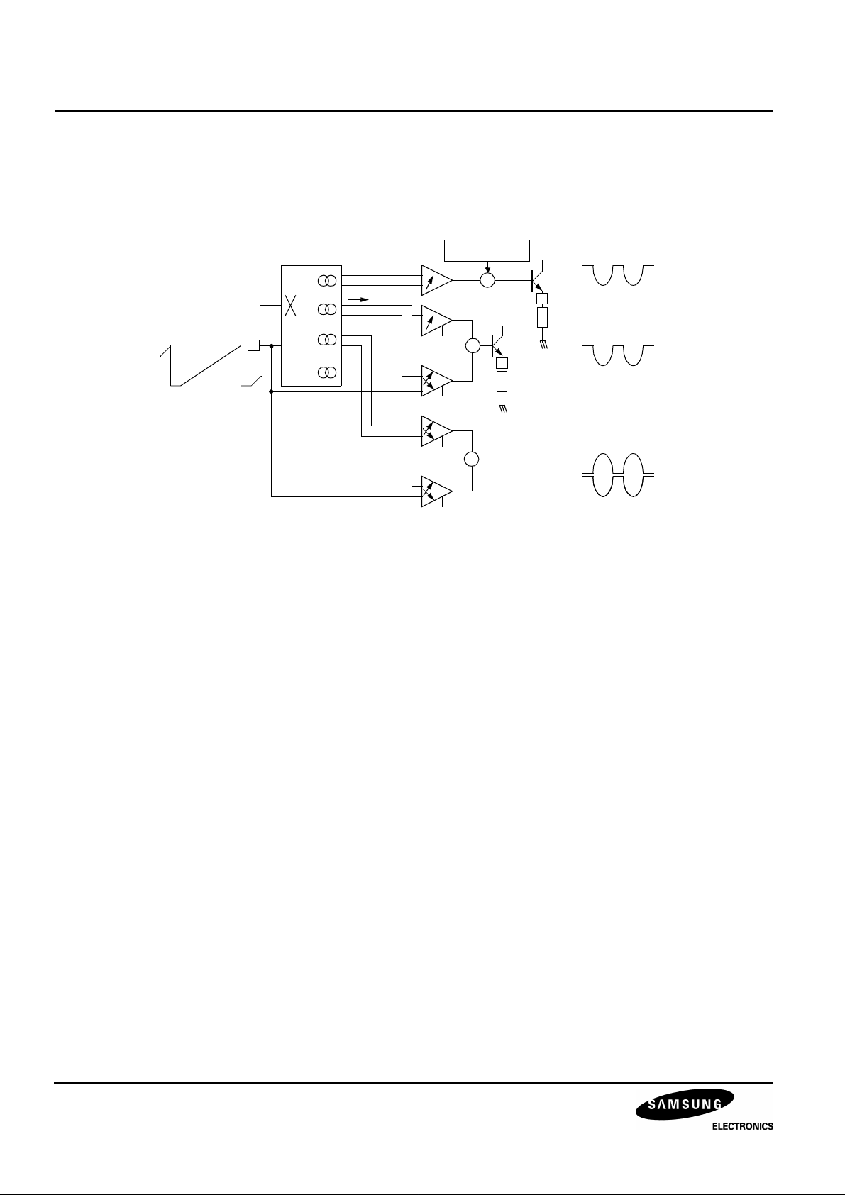
DEFLECTION PROCESSOR FOR MULTISYNC MONITORS S1D2511B01
VDF
DC
VDF
AMP
B
A
Figure 1. Vertical Dynamic Focus Function
EW
PARA
B
A
EW
DC
Figure 2. E/W Output
EW
PARA
B
A
SPB
PARA
DHPC
PC
Figure 3. Dynamic Horizontal Phase Control Output
17

S1D2511B01 DEFLECTION PROCESSOR FOR MULTISYNC MONITORS
Function
Sub
address
Pin Byte Specification Picture Image
Vertical Size 05 23
Vertical
Position
DC
06 23
Control
Vertical
S
07 23
Linearity
10000000
11111111
x0000000
x1000000
x1111111
x0xxxxxx
Inhibited
x1111111
V
OUTDC
V
OUTDC
Vpp
3.2V
3.5V
3.8V
∆V
∆V
Vpp
2.25V
3.75V
=4%
Vertical
C
Linearity
08 23
Figure 4. Typical Vertical Output Waveforms
x1000000
x1111111
Vpp
Vpp
∆V
∆V
∆V
Vpp
∆V
Vpp
=3%
=3%
18

DEFLECTION PROCESSOR FOR MULTISYNC MONITORS S1D2511B01
Function
Key Stone
(Trapezoid)
Control
E/W
(Pin Cushion)
Control
Parallelogram
Control
Sub
address
09 24
0A 24
0E Internal
Pin Byte Specification Picture Image
EWamp
Typ.
10000000
1.0V
1.0V
2.5V
2.5V
1111111
Keystone
Inhibited
2.5V
0V
1x000000
1x111111
2.5V
SPB
Inhibited
3.7V
x1000000
3.7V
1.4% TH
1.4% TH
x111111
Side Pin
Balance
Control
Vertical
Dynamic
Focus
with Horizontal
0D
Parallelogram
Inhibited
Internal
x0000000
3.7V
3.7V
x1111111
32
2V
Figure 5. Geometry Output Waveforms
1.4% TH
1.4% TH
19

S1D2511B01 DEFLECTION PROCESSOR FOR MULTISYNC MONITORS
I2C BUS ADDRESS TABLE
Slave Address (8C): Write Mode
Sub Address Definition
D8 D7 D6 D5 D4 D3 D2 D1
0 0 0 0 0 0 0 0 0 Horizontal drive selection/horizontal duty cycle
1 0 0 0 0 0 0 0 1 Horizontal position
2 0 0 0 0 0 0 1 0 Forced frequcny /free running frequency
3 0 0 0 0 0 0 1 1 Synchro priority / horizontal focus amplitude
4 0 0 0 0 0 1 0 0 Refresh /horizontal focus keystone
5 0 0 0 0 0 1 0 1 Vertical ramp amplitude
6 0 0 0 0 0 1 1 0 Vertical position adjustment
7 0 0 0 0 0 1 1 1 S Correction
8 0 0 0 0 1 0 0 0 C Correction
9 0 0 0 0 1 0 0 1 E/W keystone
A 0 0 0 0 1 0 1 0 E/W amplitude
B 0 0 0 0 1 0 1 1 B+ reference adjustment
C 0 0 0 0 1 1 0 0 Vertical moire
D 0 0 0 0 1 1 0 1 Side pin balance
E 0 0 0 0 1 1 1 0 Parallelogram
F 0 0 0 0 1 1 1 1 Vertical dynamic focus amplitude
Slave Address (8D): Read Mode
No Sub Address needed
20

DEFLECTION PROCESSOR FOR MULTISYNC MONITORS S1D2511B01
I2C BUS ADDRESS TABLE (continued)
D8 D7 D6 D5 D4 D3 D2 D1
WRITE MODE
00
01
02
03
04
05
06
07
08
09
0A
0B
0C
0D
0E
0F
HDrive
0, off
[1],on
Xray
1,reset
[0]
Forced frequency Free running frequency
1,on,
[0],off
Sync
0, comp
[1], sep
Detect
refresh
[0], off
Vramp
0, off
[1], on
S Select
1, on
[0]
C Select
1, on
[0]
EW key
0, off
[1]
EW sel
0, off
[1]
Test H
1, on
[0], off
Test V
1, on
[0], off
SPB sel
0, off
[1]
Parallelo
0, off
[1]
[1] [0] [0] [0] [0] [0] [0]
1,F0x2
[0],F0x3
[1] [0] [0] [0] [0] [0] [0]
[1] [0] [0] [0] [0] [0] [0]
[1] [0] [0] [0] [0] [0]
[1] [0] [0] [0] [0] [0]
[1] [0] [0] [0] [0] [0]
[1] [0] [0] [0] [0] [0] [0]
[1] [0] [0] [0] [0] [0] [0]
Moire 1, on
[0]
[1] [0] [0] [0] [0] [0]
[1] [0] [0] [0] [0] [0]
[1] [0] [0] [0] [0] [0]
[0] [0] [0] [0] [0]
Horizontal phase adjustment
[0] [0] [0] [0] [0]
[1] [0] [0] [0] [0]
[1] [0] [0] [0] [0]
Vertical ramp amplitude adjustment
Vertical position adjustment
East/West amplitude
B+ reference adjustment
[0] [0] [0] [0] [0]
Vertical dynamic focus amplitude
Horizontal duty cycle
Horizontal focus amplitude
Horizontal focus keystone
S Correction
C Correction
East/West keystone
Vertical Moire
Side pin balance
Parallelogrm
21

S1D2511B01 DEFLECTION PROCESSOR FOR MULTISYNC MONITORS
READ MODE
Polarity detection Synchro detection
H/V pol
[1],negative
V pol
[1], negative
Vext det
[0],no det
H/V det
[0],no det
V det
[0], nodet
00
Hlock
0, on
[1], no
Vlock
0, on
[1], no
Xray
1,on
[0],off
[ ] initlal value
OPERATING DESCRIPTION
GENERAL CONSIDERATIONS
Power Supply
The typical values of the power supply voltages Vcc and VDD are respectively 12V and 5V. Perfect operation is
obtained if Vcc and VDD are maintened in the limits: 10.8 to 13.2V and 4.5 to 5.5V.
In order to avoid erratic operation of the circuit during transient phase of Vcc switching on, or switching off, the
value of Vcc is monitored and the outputs of the circuit are inhibited if Vcc is less than 7.5V typically.
In the same manner, VDD is monitored and internal set-up is made until VDD reaches 4V (see I2C control table for
power on reset).
In order to have a very good power supply rejection, the circuit is internally powered by several internal voltage
references (the unigue typical value of which is 8V). Two of these voltage references are externally accessible, one
for the vertical part and on one for the horizontal one. If needed, these voltage references can be used (until Iload
is less than 5mA). Furthermore it is necessary to filter the a.m. voltage references by the use of external capacitor
connected to ground, in order to minimize the noise and consequently the “jitter” on vertical and horizontal output
signals.
I2C Control
KB2511 belongs to the I2C controlled device family, instead of being controlled by DC voltage on dedicated control
pins, each adjustment can be realized through the I2C interface. The I2C bus is a serial bus with a clock and a data
input. The general function and the bus protocol are specified in the philips-bus data sheets.
The interface (data and clock) is TTL-level compatible. The internal threshold level of the input comparator is 2.2V
(when VDD is 5V). Spikes of up to 500ns are filtered by an integrator and maximum clock speed is limited to
400kHz.
The data line (SDA) can be used in a bidirectional way that means in read-mode the IC clocks out a reply information (1byte) to the micro-processor.
The bus protocol prescribes always a full-byte transmission. The first byte after the start condition is used to transmit the IC-address (hexa 8C for write, 8D for read).
Write Mode
In write mode the second byte sent contains the subaddress of the selected function to adjust (or controls to affect)
and the third byte the corresponding data byte. It is possible to send more than one data byte to the IC. If after the
third byte no stop or start condition is detected, the circuit increments automatically the momentary subaddress in
the subaddress counter by one (auto-increment mode). So it is possible to transmit immediately the next data
bytes without sending the IC address or subaddress. It can be useful so as to reinitialize the whole controls very
quickly (flash manner). This procedure can be finished by a stop condition.
The circuit has 16 adjustment capabilities: 3 for horizontal part, 4 for vertical one, 2 for E/W correction, 2 for the
dynamic horizontal phase control, 1 for moire option, 3 for horizontal and vertical dynamic focus and 1 for B+
reference adjustment.
17 bits are also dedicated to several controls (ON/OFF, horizontal forced frequency, sync priority, detection
refresh and Xray reset).
22

DEFLECTION PROCESSOR FOR MULTISYNC MONITORS S1D2511B01
Read Mode
During read mode the second byte transmits the reply information.
The reply byte contains horizontal and vertical lock/unlock status, Xray activated or not, the horizontal and vertical
polarity detection. It also contains synchro detection status that is useful for µP to assign sync priority.
A stop condition always stops all activities of the bus decoder and switches the data and the clock line (SDA and
SCL) to high impedance.
See I2C subaddress and control tables.
Sync processor
The internal sync processor allows the S1D2511B01 to accept any kind of input synchro signals:
- separated horizontal & vertical TTL-compatible sync signals,
- composite horizontal & vertical TTL-compatible sync signals.
Sync identification Status
The MCU can read (address read mode : 8D) the status register via the I2C bus, and then select the sync priority
depending on this status.
Among other data this register indicates the presence of sync pulses on H/HVIN, VSYNCIN and(when 12V is supplied) whether a Vext has been extracted from H/HVIN. Both horizontal and vertical sync are detected even if only
5V is supplied.
In order to choose the right sync priority the MCU may proceed as follows(see I2C Address Table):
- refresh the status register,
- wait at least for 20ms(MAX. vertical period),
- read this status register,
Sync priotity choice should be:
Vext det H/V det V det Sync priority subaddress 03 (D8) Comment sync type
No Yes Yes 1 Separated H & V
Yes Yes No 0 Composite TTL H & V
Of course, when choice is made, one can refresh the sync detections and verify that extracted Vsync is present
and that no sync change occured.
Sync processor is also giving sync polarity information.
IC status
The IC can inform the MCU about the 1st horizontal PLL and vertical section status, and about the Xary protection
(activated or not). Resetting the XRAY internal latch can be done either by decreasing the Vcc supply or directly
resetting it via the I2C interface.
Sync Inputs
Both H/HVin and Vsyncin inputs are TTL compatible trigger with hysterisis to avoid erratic detection.
Both inputs include a pull up register connected to VDD.
Sync Processor Output
The sync processr indicates on the HLOCKOUT Pin whether 1st PLL is locked to an incoming horizontal sync.
HLOCKOUT is a TTL compatible CMOS output. Its level goes to high when locked. In the same time the D8 bit of
the status regiser is set to 0. This information is mainly used to trigger safety procedures(like reducing B+ value) as
soon as a change is detected on the incoming sync. Further to this, it may be used in an automatic procedure for
23

S1D2511B01 DEFLECTION PROCESSOR FOR MULTISYNC MONITORS
free running frequency(fo) adjustment.
Sending the desired fo on the sync input and progressively decreasing the free running frequently I2C register
value(address 02), the HLOCKOUT Pin will go high as soon as the proper setting is reached. Setting the free running frequency this way allows to fully exploit the S1D2511B01 horizontal frequency range.
HORIZONTAL PART
Internal input conditions
Horizontal part is internally fed by synchro processor with a digital signal corresponding to horizontal synchro
pulses or to TTL composite input.
concerning the duty cycle of the input signal, the following signals (positive or negative)may be applied to the
circuit.
Using internal integration, both signals are recognized on condition that Z/T < 25%, synchronisation occurs on the
leading edge of the internal sync signal. The minimum value of Z is 0.7µs.
Z
T
Z
Figure 6.
An other integration is able to extract vertical pulse of composite synchro if duty cycle is more than 25% (typically
d = 35%)
(7)
c
TRAMEXT
d
d
Figure 7.
The last feature performed is the equalizing pulses removing to avoid parasitic pulse on phase comparator input
which is intolerent to wrong or missing pulse.
PLL1
The PLL1 is composed of a phase comparator, an external filter and a voltage control oscillator (VCO).
The phase comparator is a phase frequency type designed in CMOS technology. This kind of phase detector
avoids locking on false frequencies. It is followed by a charge pump, composed of two current sources sunk and
sourced (I = 1mA typ. when locked, I = 140mA when unlocked). This difference between lock/unlock permits a
smooth catching of horizontal frequency by PLL1. This effect is reinforced by an internal original slow down system
when PLL1 is locked avoiding horizontal too fast frequency change.
The dynamic bahaviour of the PLL is fixed by an external filter which integrates the current of the charge pump.
A CRC filter is generally used (see figure 8 )
24

DEFLECTION PROCESSOR FOR MULTISYNC MONITORS S1D2511B01
PLL1F
7
1.8KΩ
4.7uF 1uF
Figure 8.
PLL1 is internally inhibited during extracted vertical sync (if any) to avoid taking in account missing pulses or wrong
pulse on phase comparator. The inhibition results from the opening of a switch located between the charge pump
and the filter (see figure 9 ).
The VCO uses an external RC network. It delivers a linear sawtooth obtained by charge and discharge of the
capacitor, by a current proportionnal to the current in the resistor. Typical thresholds of sawtooth are 1.6V and
6.4V.
HSYNC
INPUT
INTERFACE
TRAMEXT
H-LOCKCAP
8
LOCKDET
High
COMP1
E2
Low
Figure 9. Block Diagram
LOCK/UNLOCK
STATUS
CHARGE
PUMP
PHASE
ADJUST
TRAMEXT
PLL
INHIBITION
PLL1F R0 C0
7 8 9
I2C
SMFE
MODE
I2C
HPOS
Adj.
VCO
OSC
25

S1D2511B01 DEFLECTION PROCESSOR FOR MULTISYNC MONITORS
6.4V
1.6V
6.4V
1.6V
+
-
+
-
RS
FLIP
FLOP
0.84T0 T
Loop
7
Filter
(1.3V < V7 < 6V)
I2C Free running
Adjustment
+
-
(0.80<a<1.30)
6
R0
I
D
2
I
a
D
4 I
0
2
5
Co
Figure 10. Details of VCO
The control voltage of the VCO is typically comprised between 1.33V and 6V (see figure 10). The theorical
frequency range of this VCO is in the ratio 1 to 4.5, the effective frequency range has to be smaller 1 to 4.2 due to
clamp intervention on filter lowest value. To avoid spread of external components and the circuit itself, it is possible
to adjust free running frequency through I2C. This adjustment can be made automatically on the manufacturing line
without manual operation by using hlock/unlodk information. The adjustment range is 0.8 to 1.3 F0 (where 1.3 F0 is
the free running frequency at power on reset).
The sync frequency has to be always higher than the free running frequency. As an example for a synchro range
from 24kHz to 100kHz, the suggested free running frequency is 23kHz.
An other feature is the capability for MCU to force horizontal frequency throw I2C to 2xF0 or 3xF0 (for burn in mode
or safety requirement). In this case, inhibition switch is opened leaving PLL1 free but voltage on PLL1 filter is
forced to 2.66V for 2xF0 or 4.0V for 3xF0.
The PLL1 ensures the coincidence between the leading edge of the synchro signal and a phase reference
obtained by comparism between the sawtooth of the VCO and an internal DC voltage I2C adjustable between
2.65V and 3.75V (corresponding to ±10%) (see figure 11)
H Osc
Sawtooth
7/8T
H
1/8T
H
6.4V
2.65V < Vb < 3.75V
Vb
Phase REF1
1.6V
H Synchro
Figure 11. PLL1 Timing Diagram
26
Phase REF1 is obtained by comparision between the sawtooth and a DC
voltage adjustable between 2.6V and
3.8V. The PLL1 ensures the exact
coindidence between the signals
phase REF and HSYNS. A ±TH/10
phase adjustment is possible

DEFLECTION PROCESSOR FOR MULTISYNC MONITORS S1D2511B01
The S1D2511B01 also includes a lock/unlock identification block which senses in real time whether PLL1 is locked
or not on the incoming horizontal sync signal. The resulting information is available on Hlockout (see sync processor). The block function is described in figure 12.
When PLL1 is unlocked, It forces Hlockout to leave high.
The lock/unlock information is also available throw I2C read.
PLL2
The PLL2 ensures a constant position of the shaped flyback signal in comparism with the sawtooth of the VCO
(figure 12).
The phase comparator of PLL2 (phase type comparator) is followed by a charge pump(typical output current:0.5mA).
The flyback input is composed of an NPN transistor. This input must be current driven. The maximum
recommanded input current is 5mA (see figure 13).
The dury cycle is adjustable through I2C from 30% to 60%. For startup safe operation, initial duty cycle (after power
on reset) is 60% in order to avoid having a too long conduction period of the horizontal scanning transistor. The
maximum storage time(Ts MAX.) is (0.38TH-T
is around 28% of TH.
H Osc
Sawtooth
/2). Typically, T
FLY
7/8T
H
1/8T
/TH is around 20% which means that Ts max
FLY
H
6.4V
3.7V
1.6V
Flyback
Internally
Shaped Flyback
H drive
Ts
Duty Cycle
Figure 12. PLL2 Timing Diagram
400Ω
HFLY
12
Q1
20KΩ
GND 0V
Figure 13. Flyback Input Electrical Diagram
27

S1D2511B01 DEFLECTION PROCESSOR FOR MULTISYNC MONITORS
Output Section
The H-drive signal is transmitted to the output through a shaping block ensuring TS and I2C adjustable duty cycle.
In order to secure scanning power part operation, the output is inhibited in the following circumstances:
- Vcc too low
- Xray protection activated
- During horizontal flyback
- H Drive I2C bit control is off.
The output stage is composed of a NPN bipolar transistor. Only the collector is accessible (see figure 14).
26 H-DRIVE
Figure 14.
The output NPN is in off-state when the power scanning transistor is also in off-state.
The maximum output current is 30mA, and the corresponding voltage drop of the output V
It is evident that the power scanning transistor cannot be directly driven by the integrated circuit. An interface has
to be designed between the circuit and the power transistor which can be of bipolar or MOS type.
is 0.4V typically.
CEsat
X-RAY protection
The activation of the X-ray protection is obtained by application of a high level on the X-ray input (8V on pin 25). It
inhibits the H-Drive and B+ outputs.
This protection is latched; It may be reset either by Vcc switch off or by I2C(see figure 15).
Horizontal and vertical dynamic focus
The S1D2511B01 delivers and horizontal parabola added on a vertical parabola wavefrom on pin 10. This horizontal parabola is performed from a sawtooth in phase with flyback pulse middle. This sawtooth is present on pin 9
where the horizontal focus capacitor is the same as C0 to obtain a controlled amplitude (from 2 to 4.7V typically).
Symmetry (keystone) and amplitude are I2C adjustable (see figure 16). Vertical dynamic focus is tracked with
VPOS and VAMP. Its amplitude can be adjusted. It is also affected by S and C corrections. This positive signal has
to be connected to the CRT focusing grids.
28

DEFLECTION PROCESSOR FOR MULTISYNC MONITORS S1D2511B01
Vcc checking
Vcc
VSCinh
XRAY protection
Xray
Vcc off or I2C reset
Horizontal flyback
0.7V
I2C Drive on/off
-
+
S
Q
R
-
+
Figure 15. Safety Functions Block Diagram
Horizontal flyback
Internal triggerd
Horizontal flyback
Horizontal focus
Cap Sawtooth
Horizontal dynamic
focus parabola
output
I2C ramp on/off
400ns
Moire output
HORIZONTAL
OUTPUT
INHIBITION
VERTICAL
OUTPUT
INHIBITION
BOUT
4.7V
2V
2V
Figure 16.
29
S1D2511B01 DEFLECTION PROCESSOR FOR MULTISYNC MONITORS
Parabola
V.Focus
VERTICAL PART
Geometric Corrections
The principle is represented in figure 17.
Horizontal
Dynamic Focus
+
10
Dynamic focus
V
DCMID
(3.5V)
Generator
2
AMP
I
V
DCMID
(3.5V)
sidepin amp
V
DCMID
EW amp
keystone
+
24
To horizontal
+
phase
EW output
Vertical
Ramp V
23
OUT
(3.5V)
Parallelogram
Sidepin balance
output current
Figure 17. Geometric Correcitions Principle
Starting from the vertical ramp, a parabola shaped current is generated for E/W correction, dynamic horizontal
phase control correction, and vertical dynamic focus correction.
The base of the parabola generator is an analog multiplier, the output current of which is equal to:
∆I = k• ( V
OUT
- V
DCMID
Where Vout is the vertical output ramp(typically between 2 and 5V) and V
)
2
DCMID
is 3.5V(for V
=8V). The VOUT
REF-V
sawtooth is typically centered on 3.5V. By changing the vertical position, the sawtooth shifts by ±0.3V.
In order to keep a good screen geometry for any end user preference adjustment we implemented the geometry
tracking.
Due to large output stages voltage range (E/W, FOCUS), the combination of tracking function with maximum vertical amplitude max or min vertical position and maximum gain on the DAC control may lead to the output stages
saturation. This must be avoided by limiting the output voltage by appropriate I2C registers values.
For E/W part and Dynamic Horizontal phase control part, a sawtooth shaped differential current in the following
form is generated:
∆I’ = k’ • ( V
OUT
- V
DCMID
2
)
Then ∆I and ∆I’are added together and converted into voltage for the E/W part.
Each of the two E/W components or the two Dynamic horizontal phase control ones may be inhibited by their own
I2C select bit.
The E/W parabola is available on pin 24 by the way of an emitter follower which has to be biased by an external
resistor (10KΩ). It can be DC coupled with external circuitry.
Vertical dynamic focus is combined with horizontal one on output pin 10. Dynamic horizontal phase control current
drives internally the H-position, moving the Hfly position on the horizontal sawtooth in the ± 1.4% Th both on side
pin balance and parallelogrm.
30

DEFLECTION PROCESSOR FOR MULTISYNC MONITORS S1D2511B01
EW
EWOUT = 2.5V + K1 ( V
OUT
- V
DCMID
)2 + K2 ( V
OUT
- V
DCMID
)
K1 is adjustable by EW amplitude I2C register
K2 is adjustable by keystone I2C register
Dynamic horizontal phase control
IOUT = K3 ( V
OUT
- V
DCMID
) 2 + K4 ( V
OUT
- V
DCMID
)
K4 is adjustable by side pin balance I2C register
K3 is adjustable by parallelogram I2C register.
Function
When the synchronisation pulse is not present, an internal current source sets the free running frequency. For an
external capacitor, C
= 150nF, the typical free running frequency is 100Hz.
OSC
Typical free running frequency can be calculated by:
f0 (Hz)= 1.5•10-5 •
C
1
OSC
A negative or positive TTL level pulse applied on pin 2 (VSYNC) as well as a TTL composite sync on pin 1 can synchronise the ramp in the range [fmin, fmax]. This frequency range depends on the external capacitor connected on
pin 22. A capacitor in the range [150nF, 220nF] ± 5% is recommanded for application in the following range: 50Hz
to 165Hz.
Typical maximum and minimum frequency, at 25°C and without any correction (S correction or C correction), can
be calculated by:
f
= 2.5 x f0 and f
(Max.)
(Min.)
= 0.33 x f
0
If S or C corrections are applied, these values are slighty affected.
If a synchronisation pulse is applied, the internal oscillator is automaticaly caught but the amplitude is no more constant. An internal correction is activated to adjust it in less than a half a second : the highest voltage of the ramp pin
22 is sampled on the sampling capacitor connected on pin 20 at each clock pulse and a transconductance amplifier generates the charge current of the capacitor. The ramp amplitude becomes again constant.
The read status register enables to have the vertical lock-unlock and the vertical sync polarity informations.
It is recommanded to use a AGC capacitor with low leakage current. A value lower than 100nA is mandatory.
Good stability of the internal closed loop is reached by a 470nF ± 5% capacitor value on pin 20 (VAGC)
31

S1D2511B01 DEFLECTION PROCESSOR FOR MULTISYNC MONITORS
TRANSCONDUCTANCE
AMPLIFIER
REF
20
SAMP
CAP
Vlow
S CORRECTION
C CORRECTION
Switch
Dlech
VS_AMP
SUB07/8bits
COR-C
SUB08/6bits
23
18
VERT_AMP
SUB05/7BITS
VMOIRE
SUB0C/5BITS
VOSITION
SUB06/7BITS
VOUT
BREATH
2
V-SYNC
SYNCHRO OSCILLATOR
POLARITY
DISCH.
CHARGE CURRENT
-
22
+
SAMPLING
OSC
CAP
-
+
Figure 18. AGC Loop Block Diagram
I2C Control Adjustments
Then, S and C correction shapes can be added to this ramp. This frequency independent S and C corrections are
generated internally. Their amplitude are adjustable by their respective I2C register. They can also be inhibited by
their select bit. Endly, the amplitude of this S and C corrected ramp can be adjusted by the vertical ramp amplitude
control register. The adjusted ramp is available on pin 23 (VOUT) to drive an external power stage. The gain of this
stage is typically 25% depending on its register value. The mean value of this ramp is driven by its own I2C register
(vertical position). Its value is VPOS = 7/16 • V
± 300mV.
REF
Usually VOUT is sent through a resistive divider to the inverting input of the booster. Since VPOS derives from
V
, the bias voltage sent to the non-inverting input of booster should also derive from V
REF-V
to optimize the
REF-V
accuracy(see Application Diagram).
Basic Equations
In first approximation, the amplitude of the ramp on pin 23 (Vout) is:
V
- VPOS = ( V
OUT
OSC
- V
) • ( 1 + 0.25 (V
DCMID
AMP
) )
with:
- V
- V
= 7/16•V
DCMID
= V22 ( ramp with fixed amplitude)
OSC
( typically 3.5V, the middle value of the ramp on pin 22)
REF
- VAMP = - 1 for minimum vertical amplitude register value and +1 for maximum
- VPOS is calculated by : VPOS = V
+ 0.3Vp with Vp equals -1 for minimum vertical position register value
DCMID
and +1 for maximum
The current available on Pin 22 is :
I
OSC
3
= • V
8
REF
• C
OSC
• f
32

DEFLECTION PROCESSOR FOR MULTISYNC MONITORS S1D2511B01
with C
: capacitor connected on pin 22
OSC
f: synchronisation frequency.
Vertical Moire
By using the vertical moire, VPOS can be modulated from to frame. This function is intended to cancel the fringes
which appear when line to line interval is very close to the CRT vertical pitch. The amplitude pf the modulation is
controlled by register VMOIRE on sub-off via the control bit D7.
DC/DC CONVERTER PART
This unit controls the switch-mode DC/DC con-verter. It converts a DC constant voltage into the B+ voltage
(roughly proportional to the horizontal frequency)necessary for the horizontal scanning. This DC/DC converter can
be configured either in step-up or step-down mode. In both cases it oper-ates very similarly to the well known
UC3842.
Step-up Mode
Operating Description
- The powerMOSisswitched-onduringthe flyback (at the beginning of the positive slope of the horizontal focus
sawtooth).
- The power MOS is switched-off when its current reachesa predeterminedvalue. Forthispurpose, a sense resistor
is inserted in its source. The voltage on this resistor is sent to Pin16 (ISENSE).
- The feedback(coming either from the EHV or from the flyback) is divided to a voltage close to 4.8V and com pared pared to the internal 4.8V reference(IVREF). The difference is amplified by an error amplifier, the output of
which controls the power MOS switch-off current.
Main Features
- Switching synchronized on the horizontal fre-quency,
- B+ voltage always higher than the DC source, - Current limited on a pulse-by-pulse basis.
Step-down Mode
In step-down mode, the Isense information is not used any more and therefore not sent to the Pin16. This mode is
selected by connecting this Pin16 to a DC voltage higher than 6V (for example VREF-V).
Operating Description
- The powerMOSis switched-onas for thestep-up mode.
- The feedbackto the error amplifier is done as for the step-up mode.
- The power MOS is switched-off when the HFOCUSCAP voltage get higher than the error amplifier output voltage
Main Features
- Switching synchronized on the horizontal fre-quency,
- B+ voltage always lower than the DC source,
- No current limitation.
33

S1D2511B01 DEFLECTION PROCESSOR FOR MULTISYNC MONITORS
APPLICATION CIRCUIT
VCC=12V
HSYNC
VSYNC
AFC
AFC
22K
22K
4.7uF 50V
10nF 100V MP
50K
50K
1K
1K
22nF 100V
1% P
820pF 50V
6.8K
1.8K
+
1uF
820pF
10K
4.7uF
0.1uF
+
1M
33K
3.3K
1
2
3
4
5
6
7
8
9
10
11
12
13
14
15
16
HSYNC_IN
VSYNC_IN
H_LOCKOUT
PLL2C
CO
RO
PLL1F
HPOSITION
HFOCUSCAP
H_FOCUS
HGND
HFLY
H_REF
COMP
REGIN
I_SENSE
S1D2511B
KB2511B
SDA
SCL
VCC
B+OUT
GND
H_OUT
XRAY
EWOUT
VOUT
VSCAP
V_REF
VAGCCAP
VGND
BREATH
B+GND
+
100uF
100
100
+
100uF
10K
10K
150nF 100V
1% P
470nF 63V P
5V
0.1uF
SDA
SCL
0.1uF
10K
1K
HOUT
22K
50K
+47uF
0.1uF
50V
10K
1K
50K
1K
32
5V
31
30
29
28
27
26
25
24
23
22
21
20
19
18
17
1
SCLK
2
SDAT
3
ACK
4
1
2
3
4
5
6
7
74HCT125
5V
14
13
12
11
10
9
8
12V
100K
0.1uF+100uF
SCL
SDA
34
HOUT
47pF
1
2
3
4
5
6
7
8
MC14528
16
47pF
15
14
13
12
11
10K
10
33pF
9
100K
AFC
 Loading...