


查询S1D2504A01供应商
JULY. 2000
DATA SHEET
S1D2504A01
I2C BUS CONTROLLED R/G/B VIDEO AMPLIFIER S1D2504A01
I2C BUS CONTROLLED R/G/B VIDEO AMPLIFIER
The S1D2504A01 is very high frequency video amplifier system with I2C BUS control used in Monitors.
It contains 3 matched R/G/B video Amplifiers and provides
flexible interfacing to the I2C BUS controlled adjustment sys-
tems.
FUNCTIONS
• R/G/B Video Amplifier
• I2C BUS Control
• Contrast Control
• Brightness Control
• Cut-Off Brightness Control
• R/G/B SUB Contrast/Cut Off Control
• Blank/Clamp Gate
• Auto beam current limitation (ABL) is possible
with external pin.
• The S1D2504A01 includes white balance
adjustment that is effective on brightness (by
Cut-Off control for each channel).
ORDERING INFORMATION
S1D2504A01-D0B0 24-DIP-300 -20 °C — 75 °C
24-DIP-300
Device Package Operating Temperature
FEATURES
• 3-Channel matched R/G/B Video Amplifiers
• I2C BUS control items
– Contrast control for the 3 channels
– Brightness control for the 3 channels
– SUB Contrast control for each channel
– Cut-Off control for each channel
– Cut-Off Brightness control for the 3 channels
– Switch Registers for SBLK and Cut-Off Offset Current
• Built-in ABL (Automatic Beam Limitation)
• Built-in Video output Brightness clamp
• 3-Channel R/G/B Video Amplifier 85 MHz @f-3 dB
• Contrast Control Range: -38 dB
• SUB Contrast Control Range: -11 dB
• Capable of 7 Vpp Output Swing
1

S1D2504A01 I2C BUS COTROLLED R/G/B VIDEO AMPLIFIER
BLOCK DIAGRAM
ONE (RED)
VCC1
RIN
GND1
OF THREE CHANNELS
1
2
VIDEO
CONTRAST
SUB
CONTRAST
A1
3
BLK
A2
A3
CLP
gm2
ROUT
23
RCLP
24
_
+
16
RCT
GIN
GND2
BIN
VCC2
GND(L)
ABL
SCL
SDA
10
11
4
2.4V
5
BLK
CLP
CT
OFFSET
+ +
CUT OFF
CT BRT
6
7
CUT OFF OFFSET D6:5 (01H)
9
CONTRAST (00H)
G DRIVE (03H)
R DRIVE (02H)
BRIGHTNESS (01H)
B DRIVE (04H)
G CUT OFF (07H)
R CUT OFF (06H)
8
CUT OFF BRIGHT (05H)
B CUT OFF (08H)
CLAMP
GATE
21
22
15
18
17
14
20
19
12
GOUT
GCLP
GCT
BOUT
BCLP
BCT
VCC3
GND3
CLP
I2C BUS CONTROL
SOFT BLANK
D7 (01H)
BLANK
GATE
CONTROL
13
BLK
2
I2C BUS CONTROLLED R/G/B VIDEO AMPLIFIER S1D2504A01
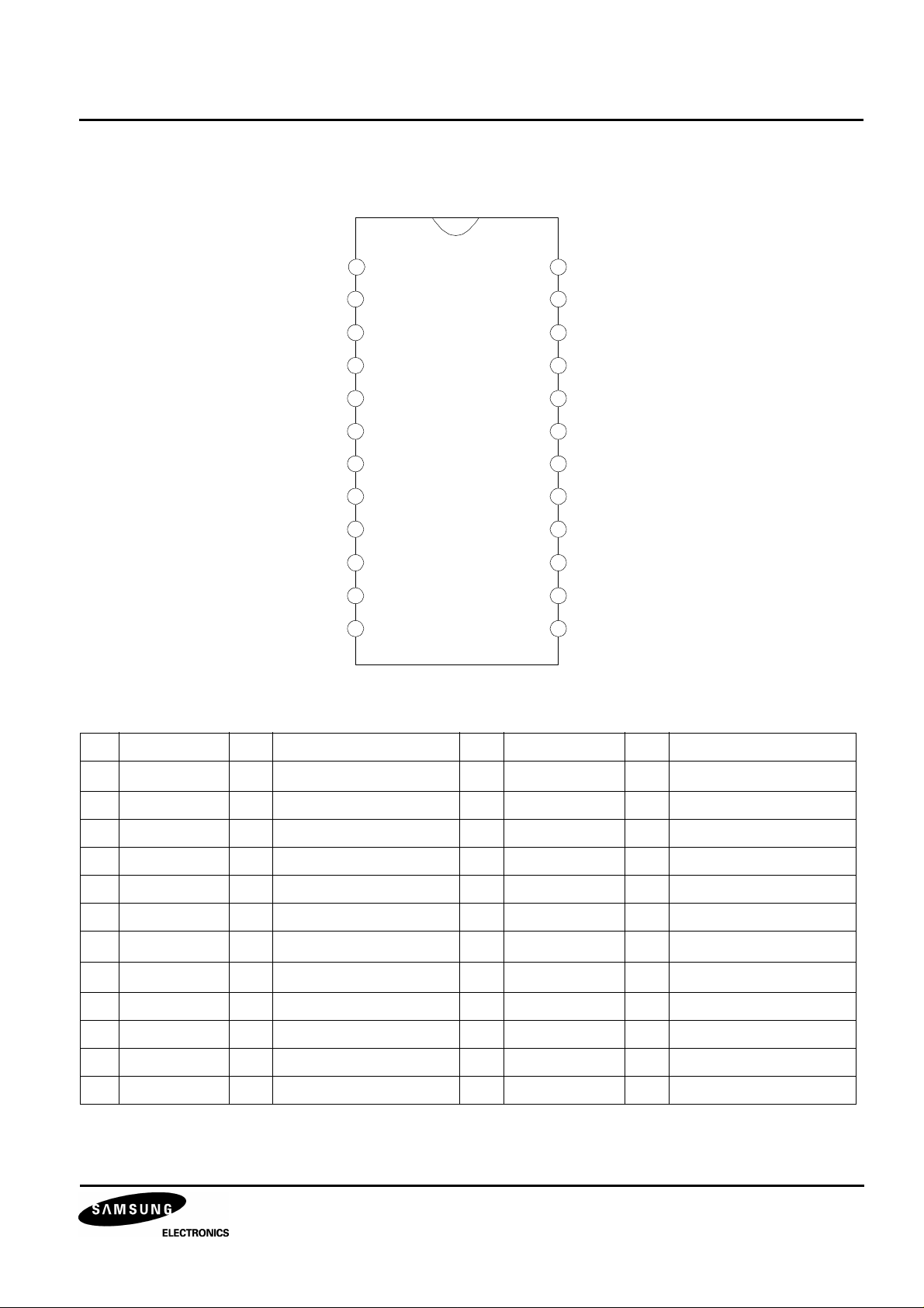
PIN CONFIGURATION
10
11
12
1
2
3
4
5
6
7
8
9
VCC1
RIN
GND1
GIN
GND2
BIN
VCC2
ABL
GND(L)
SCL
SDA
CLP
S1D2504A01
KA2504
RCLP
ROUT
GCLP
GOUT
VCC3
GND3
BOUT
BCLP
RCT
GCT
BCT
BLK
24
23
22
21
20
19
18
17
16
15
14
13
Table 1. Pin Configuration
NO Symbol I/O Configuration NO Symbol I/O Configuration
1 VCC1 - Normal Power Supply 13 BLK I Blank Gate Input
2 RIN I Red Video Input 14 BCT I Blue Cut off ctrl
3 GND1 - Normal Ground 15 GCT I Green Cut off ctrl
4 GIN I Green Video Input 16 RCT I Red Cut off ctrl
5 GND2 - Normal Ground 17 BCLP - Blue Clamp Cap
6 BIN I Blue Video Input 18 BOUT O Blue Video Output
7 VCC2 - Normal Power Supply 19 GND3 - Drive Power Ground
8 ABL I Automatic Beam Limit 20 VCC3 - Drive Power Supply
9 GND (L) - Logic Ground 21 GOUT O Green Video Output
10 SCL I/O Serial Clock 22 GCLP - Green Clamp Cap
11 SDA I/O Serial Data 23 ROUT O Red Video Output
12 CLP I Clamp Gate Input 24 RCLP - Red Clamp Cap
3

S1D2504A01 I2C BUS COTROLLED R/G/B VIDEO AMPLIFIER
PIN DESCRIPTION
Table 2. Pin Description
Pin No Pin Name Schematic Description
1 VCC1 - Normal V
2
4
Red Video Input
(RIN)
Green Video Input
(GIN)
PIN 2
2.4V
VCC
Video Input (Maximum 0.7
Vpp)
CC
Blue Video Input
8
(BIN)
3 GND1 - Normal Ground
5 GND2 - Normal Ground
7 VCC2 - Logic V
8
VCC
CC
ABL
PIN 8
Auto Beam Limitation
(Control Range: 0.5 ~ 4.5 V )
9 GND (L) - Logic Ground
4
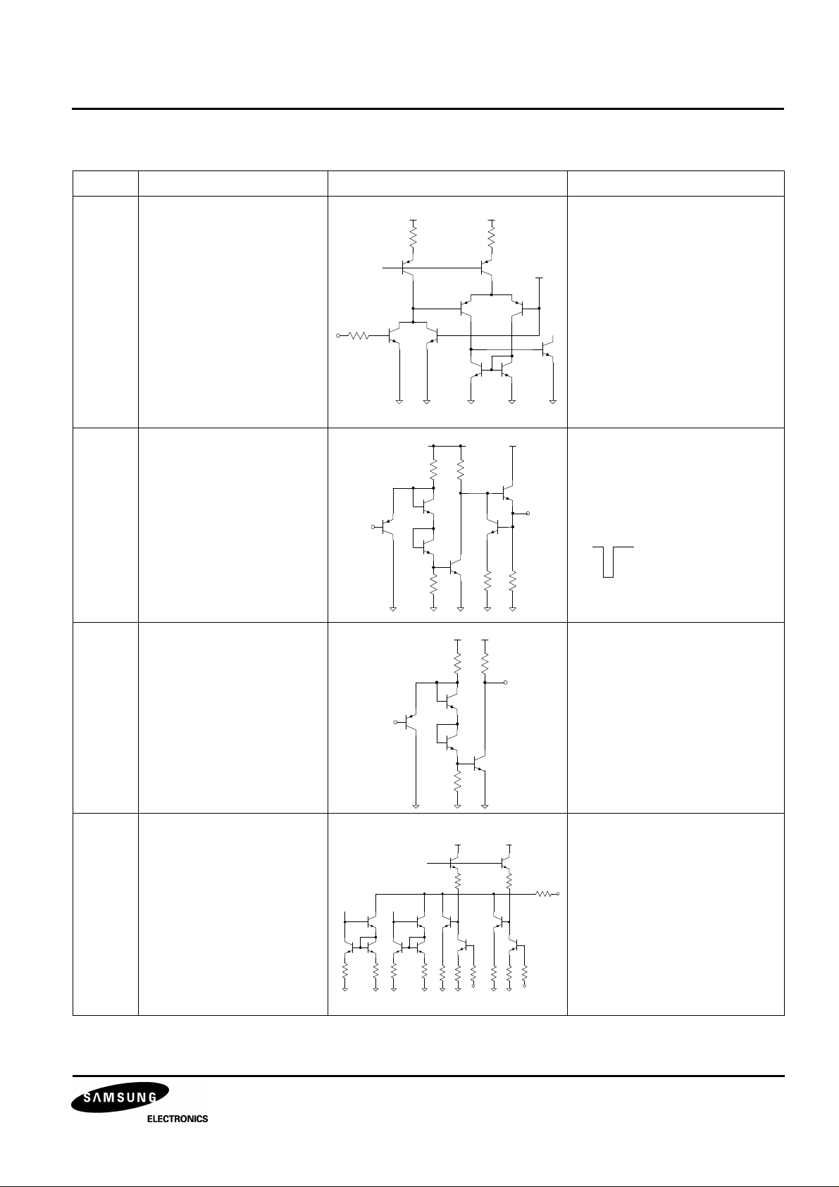
I2C BUS CONTROLLED R/G/B VIDEO AMPLIFIER S1D2504A01
PIN 10
Table 2. Pin Description (Continued)
Pin No Pin Name Schematic Description
10
11
12
Serial Clock Input
(SCL)
Serial Data Input
(SDA)
Clamp Gate Input
(CLP)
PIN12
3.2V
SCL, SDA for I2C Bus Control
VCC
5.1V
Clamp Gate Input: TTL Level
Active Low
Clamp Gate Min. Duty
f: 34 kHz
duty: 0.3 µS
13 Blank Gate Input
(BLK)
14
Blue Cut-Off
(BCT)
15
Green Cut-Off
(GCT)
16
Red Cut-Off
(RCT)
lctbrt lct
PIN13
7V VCC
CS2 CS1
Blank Gate Input: TTL Level
Active Low
vccvcc
Cut-Off Control Output
Icut-off = Ict+Ictbrt+Ics 1+Ics 2
Ict : 0 ~ 540µA
pin 14
Ictbrt: 0 ~ 160µA
Ics 1 : 80µA
Ics 2 : 160µA
5
S1D2504A01 I2C BUS COTROLLED R/G/B VIDEO AMPLIFIER
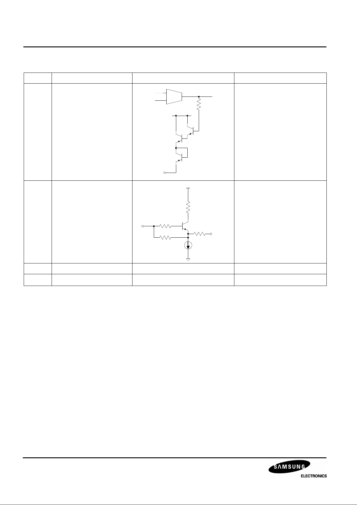
Table 2. Pin Description (Continued)
Pin No Pin Name Schematic Description
17
22
24
18
21
23
Blue Clamp Cap
(BCLP)
Green Clamp Cap
(GCLP)
Red Clamp Cap
(RCLP)
Blue Video Output
(BOUT)
Green Video Output
(GOUT)
Red Video Output
(ROUT)
Bright
Vout
+
-
PIN 17
Clamp Cap for Brightness
(During Clamp Gate Low)
vcc
Video Out
PIN 18
663uA
19 GND3 - Normal Ground
20 VCC3 - Drive V
CC
6

I2C BUS CONTROLLED R/G/B VIDEO AMPLIFIER S1D2504A01
ABSOLUTE MAXIMUM RATINGS
NO Item Symbol Value Unit
1 Normal, Logic, Driver Power Supply V
2 Maximum Power Dissipation PDmax 1.5 W
1, 2, 3 13.2 V
CC
THERMAL CHARACTERISTICS
NO Item Symbol Value Unit
1 Storage Temperature Tstg -65 — 150
2 Operating Temperature Topr -20 — 75 °C
3 Thermal Resistance (Junction ambient) θja 60.0 °C/W
4 Junction Temperature Tj 150.0 °C
ESD PARAMETER
NO Item Symbol Value Unit
1 Human Body Model
(C = 100pF, R = 1.5kΩ)
2 Machine Model
(C = 200pF, R = 0)
HBM 2000 V
MM 300 V
°
C
3 Charge Device Model CDM 800 V
I2C BUS ELECTRICAL CHARACTERISTICS
Symbol Description Min Typ Max Unit
VinH High Level Input Voltage 3.0 - - V
VinL Low Level Input Voltage - - 1.5 V
IinH High Level Input Current - - 1.0 µA
IinL Low Level Input Current - - -10 µA
fSCL SCL Clock frequency - - 200 kHz
7

S1D2504A01 I2C BUS COTROLLED R/G/B VIDEO AMPLIFIER
ELECTRICAL CHARACTERISTICS
DC Electrical Characteristics
(Tamb = 25 °C, V
= 12 V, V
CC
DD
= 12 V)
Table 3. DC Electrical Characteristics
No Parameter Symbol Value Unit
Min Typ Max
1 Supply Current I
CC
60 80 100 mA
2 Maxium Supply Curent ICC max 70 90 110 mA
3 R Input Bias Voltage VRb 2.2 2.4 2.6 V
4 G Input Bias Voltage VGb 2.2 2.4 2.6 V
5 B Input Bias Voltage VBb 2.2 2.4 2.6 V
6 R Clamp Gate Low Input Voltage V12LR 0.8 1.5 - V
7 G Clamp Gate Low Input Voltage V12LG 0.8 1.5 - V
8 B Clamp Gate Low Input Voltage V12LB 0.8 1.5 - V
9 R Clamp Gate High Input Voltage V12HR - 1.5 2.0 V
10 G Clmap Gate High Input Voltage V12HG - 1.5 2.0 V
11 B Clamp Gate High Input Voltage V12HB - 1.5 2.0 V
12 Clamp Gate Low Input Current I12L -5.0 -2.0 - µA
13 Clamp Gate High Input Current I12H - 0.01 1.0 µA
14 R Output Clamp Cap Charge Current IclampR+ 0.45 0.75 1.50 mA
15 G Output Clamp Cap Charge Current IclampG+ 0.45 0.75 1.50 mA
16 B Output Clamp Cap Charge Current IclampB+ 0.45 0.75 1.50 mA
17 R Output Clamp Cap Discharge Current IclampR- -1.50 -0.75 -0.45 mA
18 G Output Clamp Cap Discharge Current IclampG- -1.50 -0.75 -0.45 mA
19 B Output Clamp Cap Discharge Current IclampB- -1.50 -0.75 -0.45 mA
20 R Blank Gate Low Input Voltage V13LR 0.8 1.5 - V
21 G Blank Gate Low Input Voltage V13LG 0.8 1.5 - V
22 B Blank Gate Low Input Voltage V13LB 0.8 1.5 - V
23 R Blank Gate High Input Voltage V13HR - 1.5 2.0 V
24 G Blank Gate High Input Voltage V13HG - 1.5 2.0 V
25 B Blank Gate High Input Voltage V13HB - 1.5 2.0 V
26 Blank Gate Low Input Current I13L -5.0 -2.0 - µA
27 Blank Gate High Input Current
I13H
- 0.01 1.0
µA
8

I2C BUS CONTROLLED R/G/B VIDEO AMPLIFIER S1D2504A01
Table 3. DC Electrical Characteristics (Continued)
No Parameter Symbol Value Unit
Min Typ Max
28 R BRT LOW Output Voltage (POR) VOporR 0.8 1.0 1.2 V
29 G BRT Low Output Voltage (POR) VOporG 0.8 1.0 1.2 V
30 B BRT Low Output Voltage (POR) VOporB 0.8 1.0 1.2 V
31 R-G Black Level Output Voltage ∆R-GBL - 0.0 ∆0.2 V
32 G-B Black Level Output Voltage ∆G-BBL - 0.0 ∆0.2 V
33 B-R Black Level Output Voltage ∆B-RBL - 0.0 ∆0.2 V
34 R Output High Voltage VOHR 6.2 7.5 9.0 V
35 G Output High Voltage VOHG 6.2 7.5 9.0 V
36 B Output High Voltage VOHB 6.2 7.5 9.0 V
37 R Blank Output Voltage VOBR - 0.1 0.2 V
38 G Blank Output Voltage VOBG - 0.1 0.2 V
39 B Blank Output Voltage VOBB - 0.1 0.2 V
40 SCL High Input Current I10H - 0.01 1.0 µA
41 SDA High Input Current I11H - 0.01 1.0 µA
42 SCL/SDA Low Level Input Voltage VbusL - - 1.5 V
43 SCL/SDA High Level Input Voltage VbusH 3 - - V
44 R Input Resistance Rin - 10 - kΩ
45 G Input Resistance Gin - 10 - kΩ
46 B Input Resistance Bin - 10 - kΩ
47 R Spot Killer Voltage VspotR 9.2 10.4 11.2 V
48 G Spot Killer Voltage VspotG 9.2 10.4 11.2 V
49 B Spot Killer Voltage VspotB 9.2 10.4 11.2 V
50 R Center Ext. Cut -Off Output Current IctX_80R 220 270 320 µA
51 G Center Ext. Cut -Off Output Current Ictx_80G 220 270 320 µA
52 B Center Ext. Cut -Off Output Current Ictx_80B 220 270 320 µA
53 R Cut -Off Output Current Range ∆IctxR 440 540 640 µA
54 G Cut -Off Output Current Range ∆IctxG 440 540 640 µA
55 B Cut -Off Output Current Range ∆IctxB 440 540 640 µA
56 R Cut -Off BRT Output Current Range ∆IctbrtR 150 170 210 µA
57 G Cut -Off BRT Output Current Range ∆IctbrtG 150 170 210 µA
58 B Cut-Off BRT Output Current Range ∆IctbrtB 150 170 210 µA
59 R Ext. Cut-Off Offset Output Current1 Ics1R 70 85 100 µA
9

S1D2504A01 I2C BUS COTROLLED R/G/B VIDEO AMPLIFIER
Table 3. DC Electrical Characteristics (Continued)
No Parameter Symbol Value Unit
Min Typ Max
60 G Ext. Cut-Off Offset Output Current1 Ics1G 70 85 100 µA
61 B Ext.Cut-Off Offset Output Current1 Ics1B 70 85 100 µA
62 R Ext.Cut-Off Offset Output Current2 Ics2R 140 160 180 µA
63 G Ext.Cut-Off Offset Output Current2 Ics2G 140 160 180 µA
64 B Ext.Cut-Off Offset Output Current2 Ics2B 140 160 180 µA
65 R Soft Blank Output Voltage VOsoftR - 0.1 0.2 V
66 G Soft Blank Output Voltage VOsoftG - 0.1 0.2 V
67 B Soft Blank Output Voltage VOsoftB - 0.1 0.2 V
68 R Brightness High Output Voltage VOHR 2.5 3.0 3.5 V
69 G Brightness High Output Voltage VOHG 2.5 3.0 3.5 V
70 B Brightness High Output Voltage VOHB 2.5 3.0 3.5 V
Current (uA)
940uA
540
240
160
80
Cut-off Control Offset
Total Current (0uA¡-940uA)
R,G,B,Cut-off
Control Current
(0uA¡-540uA)
CS1/2 On
CS1 On
Cut-off Control Offset
Current (0uA¡-240uA)
Cut-off Bright
Control Current
(0uA¡-160uA)
(Cut-off Control Offset Current & Sink Current Waveform)
10

I2C BUS CONTROLLED R/G/B VIDEO AMPLIFIER S1D2504A01
AC Electrical Characteristics
(Tamb = 25°C, V
= 12 V, V
CC
DD
= 12 V)
Table 4. AC Electrical Characteristics
No Parameter Symbol Value Unit
Min Typ Max
71 R Video Bandwidth f-3dBR 85 - - MHz
72 G Video Bandwidth f-3dBG 85 - - MHz
73 B Video Bandwidth f-3dBB 85 - - MHz
74 R Video Amp Gain AvmaxR 15.5 17.5 19.5 dB
75 G Video Amp Gain AvmaxG 15.5 17.5 19.5 dB
76 B Video Amp Gain AvmaxB 15.5 17.5 19.5 dB
77 Max Gain Difference between R-G AMP ∆AvmaxRG -1.0 - 1.0 dB
78 Max Gain Difference between G-B AMP ∆AvmaxGB -1.0 - 1.0 dB
79 Max Gain Difference between B-R AMP ∆AvmaxBR -1.0 - 1.0 dB
80 Low Gain Difference between R-G AMP ∆AvlowRG -1.0 - 1.0 dB
81 Low Gain Difference between G-B AMP ∆AvlowGB -1.0 - 1.0 dB
82 Low Gain Difference between B-R AMP ∆AvlowBR -1.0 - 1.0 dB
83 R Sub Drive Ctrl Max. -Center AvDRmax -3 -4 -5 dB
84 G Sub Drive Ctrl Max. -Center AvDGmax -3 -4 -5 dB
85 B Sub Drive Ctrl Max. -Center AvDBmax -3 -4 -5 dB
86 R Sub Drive Ctrl Min. -Center AvDRmin -11 -8 -5 dB
87 G Sub Drive Ctrl Min. -Center AvDGmin -11 -8 -5 dB
88 B Sub Drive Ctrl Min. -Center AvDBmin -11 -8 -5 dB
89 R Contrast Ctrl Max. -Center AvCRmax -7 -6 -4 dB
90 G Contrast Ctrl Max. -Center AvCGmax -7 -6 -4 dB
91 B Contrast Ctrl Max. -Center AvCBmax -7 -6 -4 dB
92 R Contrast Ctrl Min. -Center AvCRmin - - -35 dB
93 G Contrast Ctrl Min. -Center AvCGmin - - -35 dB
94 B Contrast Ctrl Min. -Center AvCBmin - - -35 dB
95 R ABL Control Range ∆ABLR -8.5 -11.5 -14.5 dB
96 G ABL Control Range ∆ABLG -8.5 -11.5 -14.5 dB
97 B ABL Control Range ∆ABLB -8.5 -11.5 -14.5 dB
98 R Video Amp THD THDR - 1.0 5.0 %
99 G Video Amp THD THDG - 1.0 5.0 %
11

S1D2504A01 I2C BUS COTROLLED R/G/B VIDEO AMPLIFIER
Table 4. AC Electrical Characteristics (Continued)
No Parameter Symbol Value Unit
Min Typ Max
100 B Video Amp THD THDB - 1.0 5.0 %
101 R Video Rising Time trR - 4.0 5.0 nS
102 G Video Rising Time trG - 4.0 5.0 nS
103 B Video Rising Time trB - 4.0 5.0 nS
104 R Video Falling Time tfR - 4.0 5.0 nS
105 G Video Falling Time tfG - 4.0 5.0 nS
106 B Video Falling Time tfB - 4.0 5.0 nS
107 R Blank Output Rising Time trBlankR - 6.0 15.0 nS
108 G Blank Output Rising Time trBlankG - 6.0 15.0 nS
109 B Blank Output Rising Time trBlankB - 6.0 15.0 nS
110 R Blank Output Falling Time tfBlankR - 6.0 15.0 nS
111 G Blank Output Falling Time tfBlankG - 6.0 15.0 nS
112 B Blank Output Falling Time tfBlankB - 6.0 15.0 nS
113 R Blank Rising Prop. Delay trBlankPrR - 23 50 nS
114 G Blank Rising Prop. Delay trBlankPrG - 23 50 nS
115 B Blank Rising Prop. Delay trBlankPrB - 23 50 nS
116 R Blank Falling Prop. Delay tfBlankPrR - 20 45 nS
117 G Blank Falling Prop. Delay tfBlankPrG - 20 45 nS
118 B Blank Falling Prop. Delay tfBlankPrB - 20 45 nS
119 R Video Amp ISO1 10 kHz ISO1_10KR - -65 -45 dB
120 R Video Amp ISO2 10 kHz ISO2_10KG - -65 -45 dB
121 G Video Amp ISO1 10 kHz ISO1_10KB - -65 -45 dB
122 G Video Amp ISO2 10 kHz ISO2_10KR - -65 -45 dB
123 B Video Amp ISO1 10 kHz ISO1_10KG - -65 -45 dB
124 B Video Amp ISO2 10 kHz ISO2_10KB - -65 -45 dB
125 R Video Amp ISO1 10 MHz ISO1_10MR - -50 -35 dB
126 R Video Amp ISO2 10 MHz ISO2_10MR - -50 -35 dB
127 G Video Amp ISO1 10 MHz ISO1_10MG - -50 -35 dB
128 G Video Amp ISO2 10 MHz ISO2_10MG - -50 -35 dB
129 B Video Amp ISO1 10 MHz ISO1_10MB - -50 -35 dB
130 B Video Amp ISO2 10 MHz ISO2_10MB - -50 -35 dB
12

I2C BUS CONTROLLED R/G/B VIDEO AMPLIFIER S1D2504A01
FUNCTIONAL DESCRIPTION
I2C BUS Recommended Operating Conditions
Table 5. I2C BUS Recommended Operating Conditions
Symbol Description Min Typ Max Unit
VinH Input High Level Voltage 3.0 - 5.0 V
VinL Input Low Level Voltage 0 - 1.5 V
fSCL SCL Clock frequency - - 200 kHz
tBUF Hold time before a new transmission can start 1.3 - - uS
tHDS Hold time for Start conditions 0.6 - - uS
tSUP Set-Up time for Stop conditions 0.6 - - uS
tLOW The Low Period of SCL 1.3 - - uS
tHIGH The High Period of SCL 0.6 - - uS
tHDAT Hold time data 0.3 - - uS
tSUPDAT Set-Up time data 0.25 - - uS
tR Rise time of SCL - - 1.0 uS
tF Fall time of SCL - - 3.0 uS
I2C BUS Timing Requirement
Stop:Clock High
SDA
SCL
tBUF
Start:Clock High
tHDS
tLOW
tSUPDAT
tHDAT
tSUP
tHIGH
Data Change:Clock Low
Figure 1. I2C BUS Timing Requirement
Register Description
1. Contrast Adjustment (8-Bits)
The Contrast adustment is made by controlling simultaneously the gain of three internal variable gain amplifiers
through the I2C bus interface.
The Contrast adjustment allows you to cover a typical range of 38 dB.
2. Sub Contrast Adjustments (8-Bits × 3)
These Adustments are used to adjust the gain of each channel controlled by the I2C bus. The Sub Contrast
adjustment allows you to cover a typical range of 12 dB.
13

S1D2504A01 I2C BUS COTROLLED R/G/B VIDEO AMPLIFIER
3. Brightness Adjustment (5-Bits)
The Brightness adjustment controls to add the same black level (pedestal) to the 3-channel R/G/B signals by
I2C bus.
4. Cut-Off Adjustments (8-Bits × 3)
These Adjustments are used to adjust the white balance of the each channel controlled by the I2C bus.
5. Cut-Off Brightness Adjustment (8-Bits)
The Cut-Off Brightness Adjustment controls the 3-channel Cut-Off by I2C bus.
6. Slave Address
The 2-wire serial interface is an I2C BUS interface.
The Slave address of the S1D2504A01 is DCH (hexadecimal)
Bit 8 Bit 7 Bit 6 Bit 5 Bit 4 Bit 3 Bit 2 Bit 1
1 1 0
1 1 1
0 0 (W)
7. Data Transfer
All Bytes are sent MSB (Most Significant Bit) bit first and the write data transfer is closed by a STOP.
The MCU can write data into the S1D2504A01 registers.
To write data into the S1D2504A01, after a start, MCU must send :
- The I2C address slave byte with a low level for R/W bit (bit 1)
- The byte of the internal register address where the MCU wants to write data. (SUB Address)
- The Data sent to slave
- Stop
- 1-Byte Data Transfer
STA Slave ADRS W A SUB ADRS A DATA A STO
- Multi-Data Transfer
STA Slave ADRS W A Sub ADRS A DATA A Sub ADRS A DATA A - - -
- - - Sub ADRS A DATA A STO
- Automatic increment
The automatic increment feature of the slave address enables a quick slave receiver initialization within one
transmission by the I2C BUS controller.
STA Slave ADRS W A Aut o ADRS A DATA (00H) A DATA (01H) A DATA (02H) A - - -
- - - DA TA (07H) A DATA (08H) A STO
14

I2C BUS CONTROLLED R/G/B VIDEO AMPLIFIER S1D2504A01
8. I2C Write Operation: A complete data transfer
S CL
S DA
ST AR T
MSB
transfer ¡æ
Slave address Register address Data byteACK ACK ACK
LSB
W
Generated by slave
ST OP
The automatic increment feature of the sub address enables a quick slave receiver initialization within one
transmission, by the I2C Bus controller.
9. Sub Address Allocation Map (Slave address: DCH)
SUB Addres
[Hex]
Function
Initial Value
D7 D6 D5 D4 D3 D2 D1 D0
00H Contrast Control 80H
01H SBLK CS1 CS2 Brightness Control 00H
02H R Sub Contrast Control 80H
03H G Sub Contrast Control 80H
[Hex]
04H B Sub Contrast Control 80H
05H Cut-Off Brightness Control 80H
06H R Cut-Off Control 80H
07H G Cut-Off Control 80H
08H B Cut-Off Control 80H
NOTE: SBLK: Soft Blanking Switch (1: ON, 0: OFF)
CS1/2: Cut-off Control Offset Current Switch (CS1: 80µA, CS2: 160µA)
15

S1D2504A01 I2C BUS COTROLLED R/G/B VIDEO AMPLIFIER
- Contrast Register (SUB ADRS: 00H) (Vin = 0.56 Vpp, bright: 00H, sub: FFH)
Hex D7 D6 D5 D4 D3 D2 D1 D0 Contrast (Vpp) Gain (dB) Int value (Hex)
00 0 0 0 0 0 0 0 0 0 -30.0
80 1 0 0 0 0 0 0 0 1.12 11.5 O
FF 1 1 1 1 1 1 1 1 4.2 17.5
increment/bit 0.0164 -
- Brightness Register (3-ch)(SUB ADRS: 01H) (cont: 80H, sub: FFH)
Hex D4 D3
00 0 0 0 0 0 1 O
10 1 0 0 0 0 2
1f 1 1 1 1 1 3
increment/bit 0.0625
- SUB Contrast Register (R/G/B-ch)(SUB ADRS: 02/03/04H) (Vin = 0.56 Vpp, bright: 00H, cont: FFH)
Hex D7 D6 D5 D4 D3 D2 D1 D0 Sub Contrast (Vpp) Gain (dB) Int. value (Hex)
D2 D1 D0
Brightness (V) Int. value (Hex)
00 0 0 0 0 0 0 0 0 1.33 7.5
80 1 0 0 0 0 0 0 0 2.65 13.5 O
FF 1 1 1 1 1 1 1 1 4.2 17.5
increment/bit 0.0123
- Cut-Off Brightness Register (3-ch) (SUB ADRS: 05H)
Hex D7 D6 D5 D4 D3 D2 D1 D0 Cut-Off brightness (µA) Int. value (Hex)
00 0 0 0 0 0 0 0 0 0
80 1 0 0 0 0 0 0 0 90 O
FF 1 1 1 1 1 1 1 1 180
increment/bit 0.703
- Cut-Off Register (R/G/B-ch) (SUB ADRS: 06/07/08H) (cont: 80H, sub: FFH)
Hex D7 D6 D5 D4 D3 D2 D1 D0 Cut-Off (µA) Int. value (Hex)
00 0 0 0 0 0 0 0 0 0
80 1 0 0 0 0 0 0 0 270 O
FF 1 1 1 1 1 1 1 1 540
increment/bit 2.11
16

I2C BUS CONTROLLED R/G/B VIDEO AMPLIFIER S1D2504A01
APPLICATION BOARD CIRCUIT
VCC=12V
+
100uF 0.1uF
Red In
Green In
Blue In
ABL In
SCL
SDA
CLP In
BLK In
1
2
3
4
5V
SCLK
SDAT
ACK
12V
10uF
10uF
10uF
0.1uF
+
+
+
0.1uF
0.1uF
1
Vin
U?
1
VCC1
2
RIN
3
GND1
4
GIN
5
GND2
6
BIN
7
VCC2
8
ABL
9
GND(L)
10
SCL
11
SDA
12
CLP
14
13
12
11
10
9
8
KA78T05
Vout
GND
2
S1D2504A01
5V
SCL
SDA
3
KA2504
5V
0.1uF
24
RCLP
75V
75V
75V
75K
BAV21
KSP92
2.2K
75K
BAV21
KSP92
2.2K
75K
BAV21
KSP92
2.2K
Red Out
Green Out
Blue Out
+
0.47uF
50V
+
0.47uF
50V
+
50V
0.47uF
ROUT
GCLP
GOUT
VCC3
GND3
BOUT
BCLP
RCT
GCT
BCT
BLK
23
0.1uF
22
21
20
0.1uF
19
18
0.1uF
17
16
15
14
13
100
100
100
+
100uF
1uF
100V
1uF
100V
1uF
100V
12V
+
12V
+
12V
+
390
390
390
75K
KSP42
75K
KSP42
75K
KSP42
100
+
100uF
33
75
33
75
33
75
+
100uF
100
+
47uF
2K
2K
100
100
5V
100
100
74HCT125
1
2
3
4
5
6
7
17

S1D2504A01 I2C BUS COTROLLED R/G/B VIDEO AMPLIFIER
APPLICATION CIRCUIT
75V
75K
BAV21
75K
12V
KSP92
+
KSP42
1uF
75V
+
2.2K
100V
0.47uF
50V
0.1uF
100uF
+
0.1uF
75V
VCC
RIN
390
75K
0.1uF
27
ROUT
VEE
0.1uF
100uF
+
0.1uF
BAV21
75K
12V
GND
GIN
390
KSP92
+
27 0.1uF
KSP42
1uF
GOUT
100uF
+
0.1uF
+
2.2K
100V
0.47uF
50V
To Cathode
R Out
75V
0.1uF
27
GND
BIN
390
G Out
75K
GND BOUT
B Out
BAV21
75K
12V
0.1uF
KSP92
100
KSP42
+
1uF
2.2K
100V
0.47uF
50V
+
100
100
100
24
RCLP
23
ROUT
21
GCLP22GOUT
20
VCC3
VCC11RIN2GND13GIN4GND25BIN6VCC27ABL8GND(L)9SCL10SDA11CLP
VCC=12V
+
100uF 0.1uF
+
10uF
33
100uF 0.1uF
R In
75
G In
+
B In
ABL
10uF
33
SCL
+
75
SDA
CLP
BLK
18
18
19
BOUT
GND3
S1D2504A01
KA2504
+
10uF
33
12V
0.1uF
+
75
100uF
17
100
BCLP
+
47uF 0.1uF
15
RCT16GCT
100
100
14
BCT
13
BLK
12
100

I2C BUS CONTROLLED R/G/B VIDEO AMPLIFIER S1D2504A01
CHARACTERISTICS CURVE
19

S1D2504A01 I2C BUS COTROLLED R/G/B VIDEO AMPLIFIER
20

I2C BUS CONTROLLED R/G/B VIDEO AMPLIFIER S1D2504A01
21

S1D2504A01 I2C BUS COTROLLED R/G/B VIDEO AMPLIFIER
22
 Loading...