

Samsung S1D2503X01-D0B0 Datasheet

JULY. 2000
Ver 0.3
DATA SHEET
S1D2503X01-D0B0
Preliminary
Preliminary
•
Built in video input clamp, BRT clamp
I2C BUS CONTROLLED R/G/B VIDEO AMPLIFIER FOR MONITORS S1D2503X01-D0B0
I2C BUS CONTROLLED R/G/B VIDEO AMPLIFIER
32-DIP-600A
The S1D2503X01-D0B0 is a very high frequency video amplifier
system with I2C bus control used in monitors with high resolution up to
1600 × 1200.
It contains 3 matched R/G/B video amplifiers with OSD interface and
provides flexible interfacing to I2C bus controlled adjustment systems.
FUNCTIONS
• I2C bus controlled 200MHz RGB video pre-amplifier for monitors
• The S1D2503X01-D0B0 is a very high frequency video amplifier system with OSD interface controlled by I2C
bus.
• All controls and adjustments are digitally performed thanks to I2C bus.
: Contrast, brightness and DC output level of R/G/B signals common to the 3-channel and drive adjustment
(sub contrast), cut-off control (AC or DC coupling by CT bit) is separated for each channel.
• The S1D2503X01-D0B0 is included video & OSD half tone function.
• The white blance adjustment is effective on brightness, video & OSD signals.
• The S1D2503X01-D0B0 works for application using AC or DC coupled CRT driver.
• In addition to beam current limitation (ABL), OSD intensity interface and brightness uniformity (BU) interface
are possible with external pins.
ORDERING INFORMATION
Device Package Operating Temperature
S1D2503X01-D0B0 32-DIP-600A -25 °C — +80 °C
FEATURES
• 3-channel matched R/G/B Video Amplifier
• I2C BUS control items
- Contrast control
- Brightness control
- SUB contrast control for each channel
- OSD contrast control
- Cut-off control for each channel
- Brightness control for cut-off
- Switch registers for SBLK, half tone, cut-off INT/EXT,
BPS (Blank Pulse Input Polarity Selection) and CPS
(Clamp Pulse Input Polarity Selection).
• Built in clamp gate with anti OSD sagging
• Built in OSD Interface, OSD BLK
• Built in OSD Intensity Interface
• Built in ABL (Automatic Beam Limitation)
• Built in video & OSD half tone function on OSD
picture (OSD raster 8 colors and 3 raster
selection by HR/G/B)
• Built in smooth video contrast control with
external capacitor.
• 3-channel R/G/B video amplifier 200MHz
@f-3dB
• TTL OSD inputs, 80MHz bandwidth
• Contrast control range: 38dB
• SUB contrast control range: 11dB
• OSD contrast control range: 38dB
• Capable of 7Vp-p output swing
• High speed OSD BLK
1
Preliminary
Cut Off Ext Offset D3:4 (0BH)
Cut Off Int/Ext Switch D2 (0BH)
R/G/B Cut Off Control (07/08/09H)
S1D2503X01-D0B0 I2C BUS CONTROLLED R/G/B VIDEO AMPLIFIER FOR MONITORS
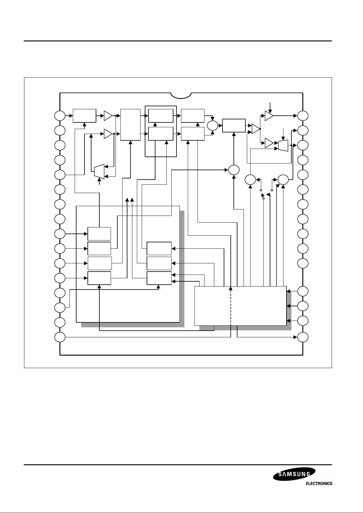
BLOCK DIAGRAM
ROSD
GOSD
BOSD
VDD
RIN
VCC1
GND1
GIN
INT
B/U
VI/
OSD_SW
CLP
BIN
One (red)
Of Three Channels
1
2
3
9
5
6
7
8
18
32
4
22
10
OSD
Interface
gm1
CLP
OSD
Intensity
B/U
Interface
Video/OSD
Switch
Clamp
Gate
Video
OSD
Switch
CLP
BLK
OSD
Raster
Video HALF-
TONE
HALF-TONE
Video
HALF-TONE
OSD Raster
Select
Blank
Gate
OSD
Contrast
Video
Contrast
Video-HALF Tone
Switch D0 (0AH)
OSD Raster Color
D1: 6 (0AH)
D4: 6 (0CH)
Soft Blank
D0 (0BH)
Blank Polarity
Select
D1 (0BH)
BLK
30
ROUT
SUB
+
Contrast
+
Contrast Contral (00H)
Cut Off
+ +
Brightness Control (01H)
R/G/B Drive Control (02/03/04H)
OSD Cont Control (05H)
CLP
gm2
31
21
27
26
25
24
19
28
29
20
Cut Off Bright (06H)
12
RCLP
RCT
VCC
GND
BOUT
BCLP
BCT
GOUT
GCLP
GCT
ABL
23
BLK
VSS
C1
11
15
Interface & Control
Clamp Polarity Select D5 (0BH)
Figure 1. Block Diagram
2
I2C Bus Control
14
SDA
13
SCL
17 DTEST
Preliminary
DTEST
I2C BUS CONTROLLED R/G/B VIDEO AMPLIFIER FOR MONITORS S1D2503X01-D0B0
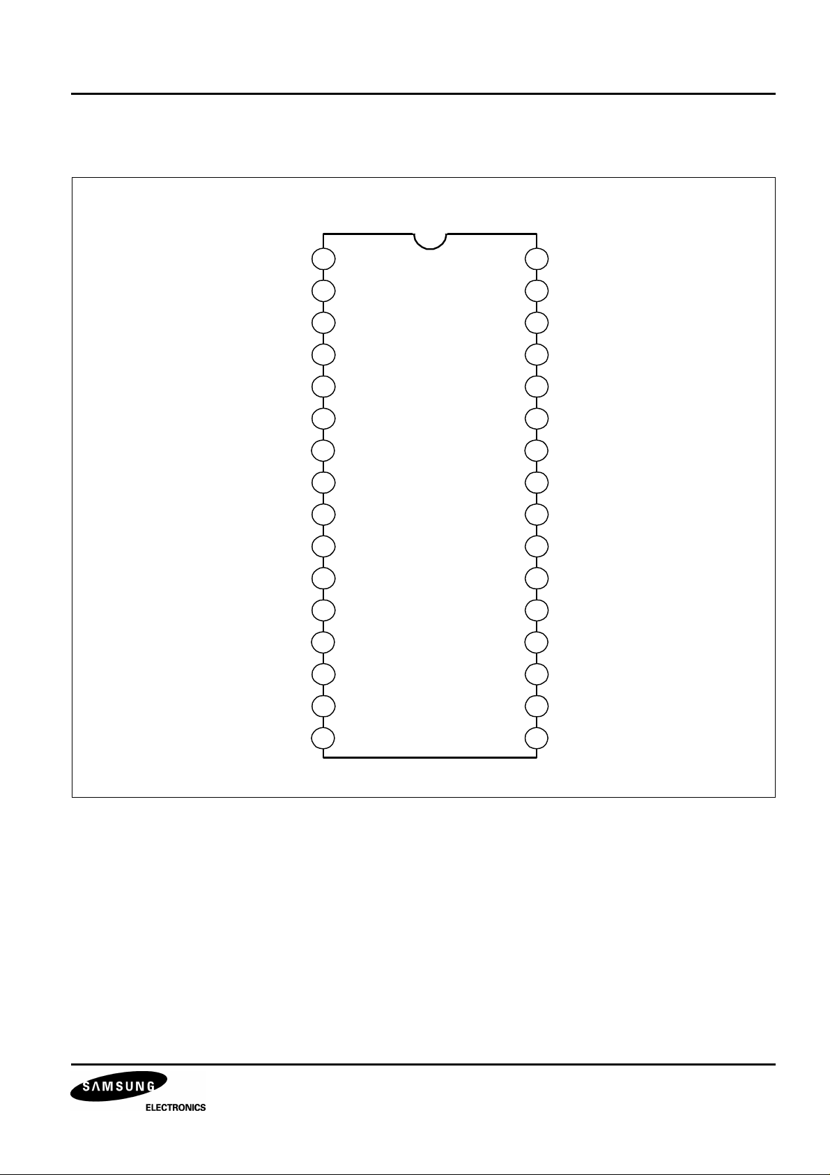
PIN CONFIGURATION
ROSD
GOSD
BOSD
VI/
OSD_SW
RIN
VCC1
GND1
GIN
VDD
BIN
VSS
ABL
SCL
10
11
12
13
1
2
3
4
5
6
7
8
32
31
30
29
28
27
26
25
B/U
RCLP
ROUT
GCLP
GOUT
VCC2
GND2
BOUT
S1D2503X01-D0B0
9
24
23
22
21
20
BCLP
BLK
CLP
RCT
GCT
14
SDA
15
C1
16 17
Figure 2. Pin Configuration
19
18
BCT
INT
3
Preliminary
S1D2503X01-D0B0 I2C BUS CONTROLLED R/G/B VIDEO AMPLIFIER FOR MONITORS
Table 1. Pin Configuration (continued)
Pin No Symbol I/O Configuration
1 ROSD I Red OSD input
2 GOSD I Green OSD input
3 BOSD I Blue OSD input
4 VI/OSD_SW I Video or OSD switch
5 RIN I Red video input
6 VCC1 - VCC (normal)
7 GND1 - Ground1 (normal)
8 GIN I Green video input
9 VDD - VDD (logic)
10 BIN I Blue video input
11 VSS - Ground (logic)
12 ABL I Automatic beam limit
13 SCL I/O Serial clock
14 SDA I/O Serial data
15 C1 - Contrast cap
16 - - 17 DTEST - 18 INT - OSD intensity
19 BCT I Blue cut off control
20 GCT I Green cut off control
21 RCT I Red cut off control
22 CLP I Clamp gate signal input
23 BLK I Blank gate signal input
24 BCLP - Blue clamp cap
25 BOUT O Blue video output
26 GND2 - Ground2 (drive part)
27 VCC2 - VCC (drive part)
28 GOUT O Green video output
29 GCLP - Green clamp cap
30 ROUT O Red video output
31 RCLP - Red clamp cap
32 B/U I Brightness uniformity
4
Preliminary
I2C BUS CONTROLLED R/G/B VIDEO AMPLIFIER FOR MONITORS S1D2503X01-D0B0
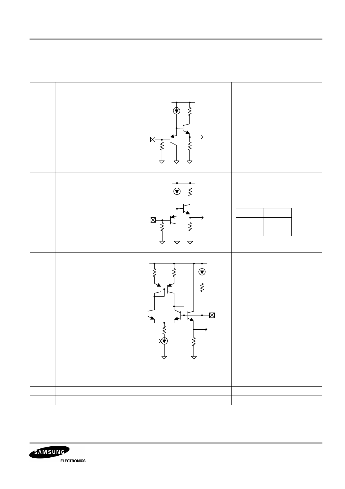
PIN DESCRIPTION
Table 2. Pin Description
Pin No Pin Name Schematic Description
1
2
Red OSD input
(ROSD)
Green OSD input
(GOSD)
OSDIN
VCC
0.2K
OSD input signals are in TTL
level and will be connected to
ground when switching to video
input
3
Blue OSD input
(BOSD)
4 Video/OSD switch
(VI/OSD_SW)
5
Red video input
(RIN)
8
Green video input
(GIN)
10
Blue video input
(BIN)
1.9V
VCC
OSDSW
VCC
1.5K
1.5K
5K100K
0.2K
5K100K
Video/OSD signal is switched by
pin4 DC level
PIN4 = “High”, OSD input
PIN4 = “Low”, video input
Pin4 Output
High OSD
Low Video
MAX input video signal is 0.7Vpp
0.2K
Video_In
0.2K
CLP
0/150uA
15K
6 VCC1 - Normal power supply (12V)
7 GND1 - Normal ground
9 VDD - Logic power supply (5V)
11 VSS - Logic ground
5
Preliminary
S1D2503X01-D0B0 I2C BUS CONTROLLED R/G/B VIDEO AMPLIFIER FOR MONITORS
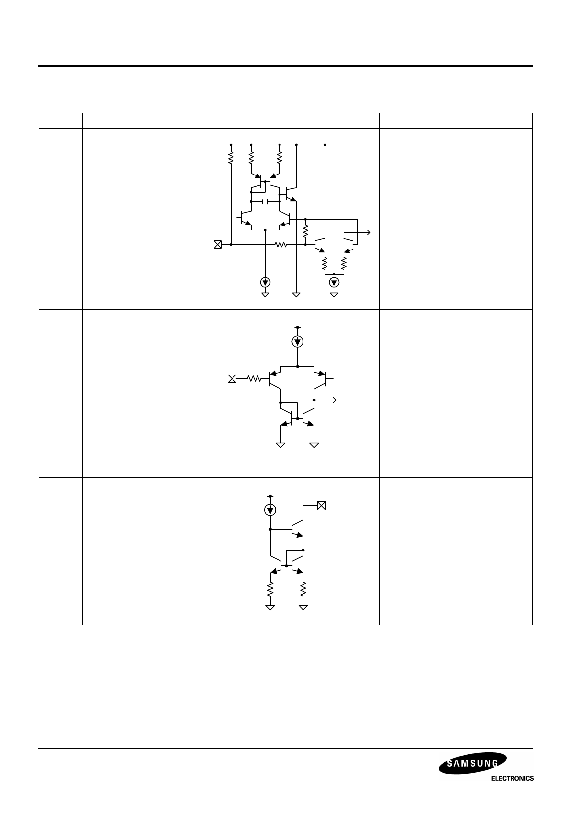
Table 2. Pin Description (Continued)
Pin No Pin Name Schematic Description
12 ABL Auto beam limitation input
VCC
100K
1K
1K
(control range: 0.5 — 4.5V)
10K
25K
2K 2K
13
14
Serial clock input
(SCL)
Serial data input
(SDA)
SCL
SDA
VDD
SCL, SDA for I2C bus control
2V
15 Contrast cap1 - External contrast cap pin
17 DAC test pin DAC current (0 - 500uA)
VCC
1K1K
6
Preliminary
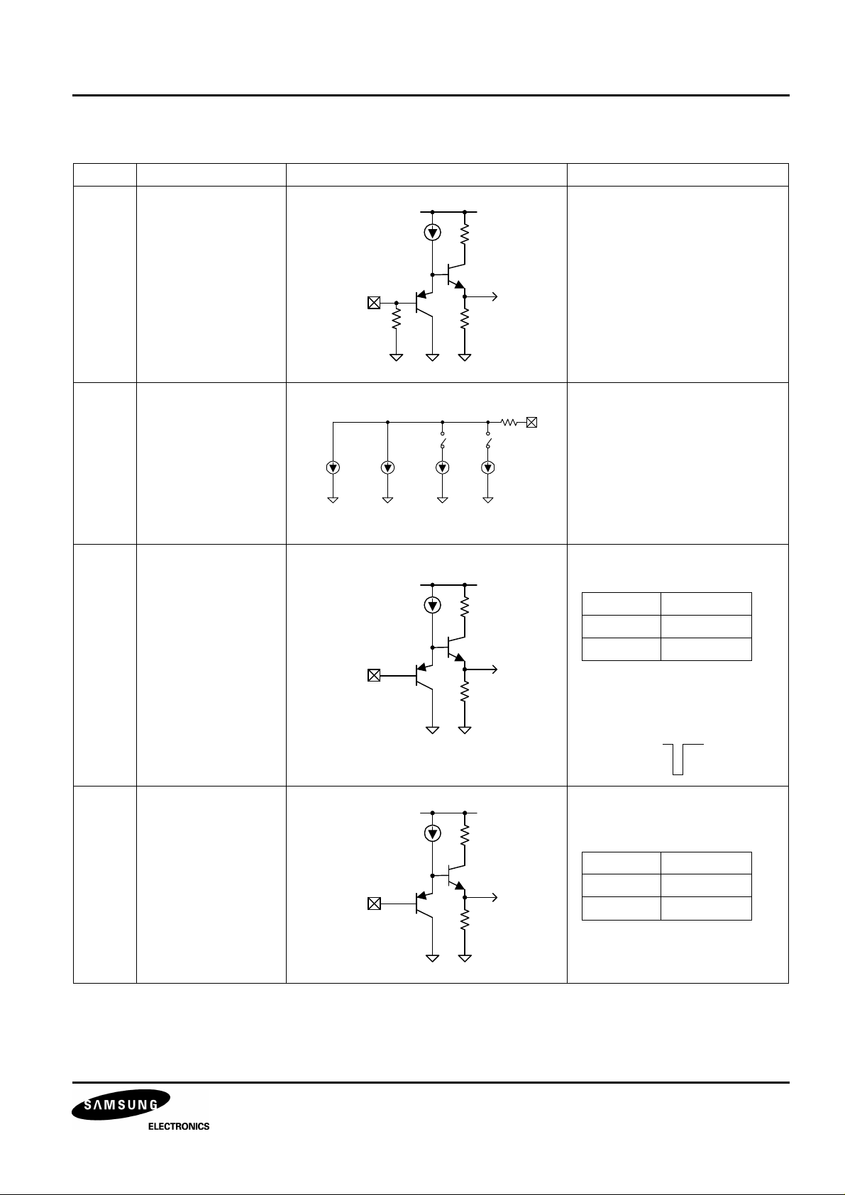
I2C BUS CONTROLLED R/G/B VIDEO AMPLIFIER FOR MONITORS S1D2503X01-D0B0
Table 2. Pin Description (Continued)
Pin No Pin Name Schematic Description
18 OSD intensity input
(INT)
VCC
0.2K
INT
5K100K
Active high
19
Blue cut-off control
(BCT)
20
Green cut-off control
(GCT)
21
Red cut-off control
(RCT)
22 Clamp gate input
(CLP)
23 Blank gate input
(BLK)
Cut-off BRT
0-200uA
CLP
Cut-off
VCC
VCC
0-500uA
100uA 100uA
CS1 CS2
0.2K
5K
0.2K
Cut-off control output
0.2K
CTX
Video amp active when clamp
gate signal is in low TTL level.
CPS Bit CLP Signal
0 Low
1 High
Clamp gate min. pulse width
: 0.2us, at fh: 50kHz
Video amp blanks video signal
when blank gate signal is in low
TTL level.
BLK
5K
BPS Bit BLK Signal
0 Low
1 High
7
 Loading...