

Samsung S1D2140B03-D0B0 Datasheet
R/G/B VIDEO AMPLIFIER WITH OSD INTERFACE FOR MONITORS S1D2140B03
R/G/B VIDEO AMPLIFIER
The S1D2140B03 is a very high frequency video amplifier system with OSD
interface intended to be used in Monitor with high resolution up to 1024 ×
768. It contains 3 matched R/G/B video Amplifiers with Blank signal and
provides a flexible interfacing to DC controlled adjustment system.
FUNCTIONS
• R/G/B Video Amplifier
• OSD Interface
• Contrast/OSD Contrast/SUB Contrast Control
ORDERING INFORMATION
• Blank/Clamp Gate
• Video Clamp
Device Package Operating Temperature
S1D2140B03-D0B0 24-DIP-300 -20 °C — +70 °C
FEATURES
• 3-Channel R/G/B Video Amplifier, 110MHz Bandwidth
• TTL OSD Input, 50MHz Bandwidth
24-DIP-300
• DC Contrast Control range: -38dB
• DC SUB Contrast Control range: -11dB
• Capable of 7.5VPP Output Swing Range
• Video/OSD high speed Switch
0
S1D2140B03 R/G/B VIDEO AMPLIFIER WITH OSD INTERFACE FOR MONITORS
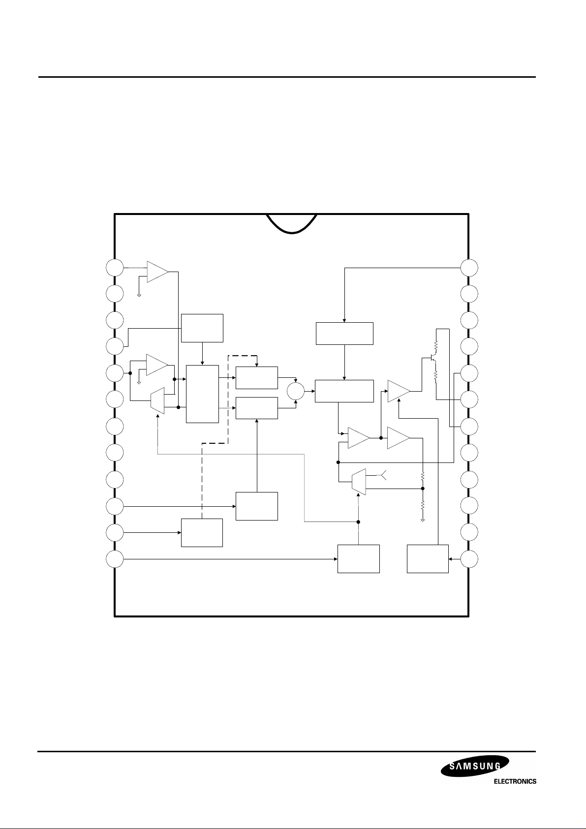
BLOCK DIAGRAM
ONE (RED)
OF THREE CHANNELS
ROSD
1
_
A1
+
24
RDRIVE
GOSD
BOSD
VI/OSD_SW
RIN
VCC1
GIN
GND1
BIN
CONST
OSD_ CONST
CLP
10
11
12
2
3
_
A2
5
6
+
gm1
_
+
7
SWITH
CONTROL
VIDEO
OSD
SWITCH
OSD
CONTRAST
VIDEO
CONTRAST
+
VIDEO
SUB_CONTRAST
CONTROL
VIDEO
SUB_CONTRAST
_
A3
+
-A5
-A4
8
_
9
CONTRAST
CONTROL
OSD
CONTRAST
CONTROL
gm2
CLAMP
GATE
1.5V
+
BLANK
GATE
23
22
21
20
19
18
17
16
15
14
13
GDRIVE
BDRIVE
GND24
RCLP
ROUT
VCC2
GCLP
GOUT
BCLP
BOUT
BLK
1
R/G/B VIDEO AMPLIFIER WITH OSD INTERFACE FOR MONITORS S1D2140B03
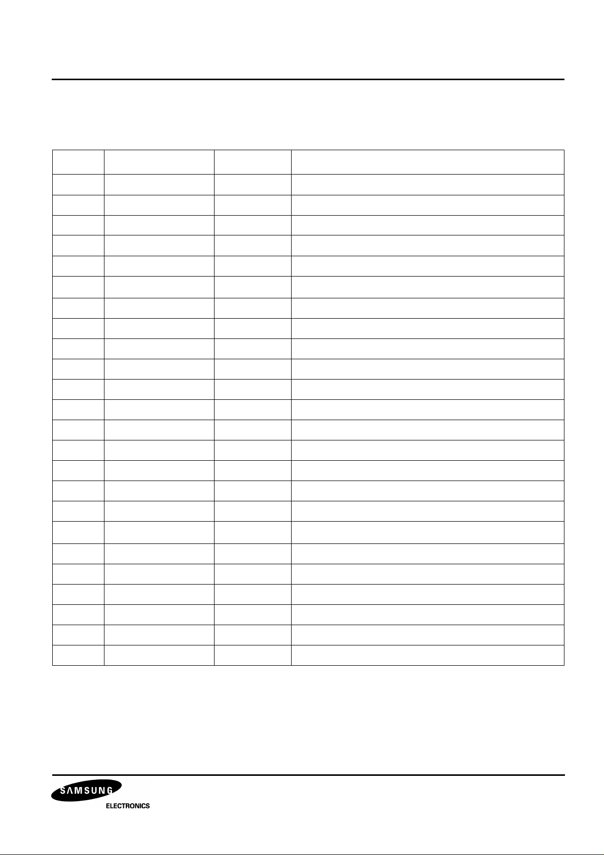
PIN CONFIGURATIONS
Table 1. Pin Configurations
Pin No Symbol I/O Configurations
1 ROSD I Red OSD Input
2 GOSD I Green OSD Input
3 BOSD I Blue OSD Input
4 VI/OSD_SW I Video or OSD Switch
5 RIN I Red Video Input
6 V
7 GIN I Green Video Input
8 GND - Ground
9 BIN I Blue Video Input
10 CONST I Contrast Control
11 OSD_CONST I OSD Contrast Control
12 CLP I Clamp Gate Signal Input
13 BLK I Blank Gate Signal Input
14 BOUT O Blue Video Output
15 BCLP - Blue Clamp Cap
16 GOUT O Green Video Output
17 GCLP - Green Clamp Cap
18 Vcc2 - VCC (output part)
19 ROUT O Red Video Output
20 RCLP - Red Clamp Cap
CC1
- VCC (normal)
21 GND - Ground
22 BDRIVE I Blue Gain Control
23 GDRIVE I Green Gain Control
24 RDRIVE I Red Gain Control
2
S1D2140B03 R/G/B VIDEO AMPLIFIER WITH OSD INTERFACE FOR MONITORS
VCC
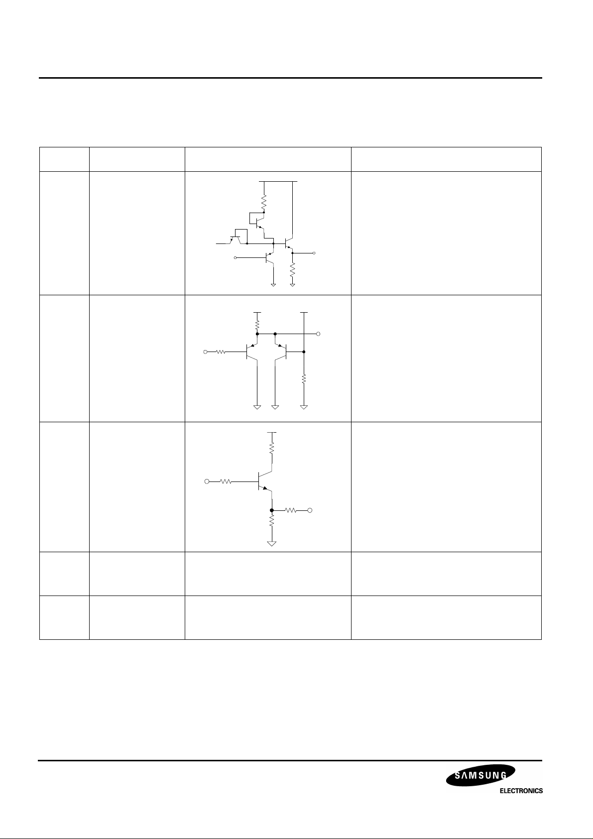
PIN DESCRIPTION
Table 2. Pin Description
Pin No Pin Name Schematic Description
VCC
1
2
3
4 Video/OSD
Red OSD Input
(ROSD)
Green OSD Input
(GOSD)
Blue OSD Input
(BOSD)
Switch
(VI/OSD_SW)
OSD input signals are in TTL level and
will be connected to ground when
switching video input
1.4V
PIN 1
5.6VVCC
Videl/OSD switch signal is TTL level
OSD Input = “High”
Video Input = “Low”
PIN 4
5
Red Video Input
MAX Input Video Signal is 0.7Vpp
(RIN)
7
Green Video Input
(GIN)
9
Blue Video Input
PIN 5
(BIN)
6 V
CC1
- Supply Voltage (except drive stage)
8 GND - Ground
3
 Loading...