

Page 1
Alignment and Adjustments
Samsung Electronics 2-1
2. Alignment and Adjustments
2-1 Service Mode
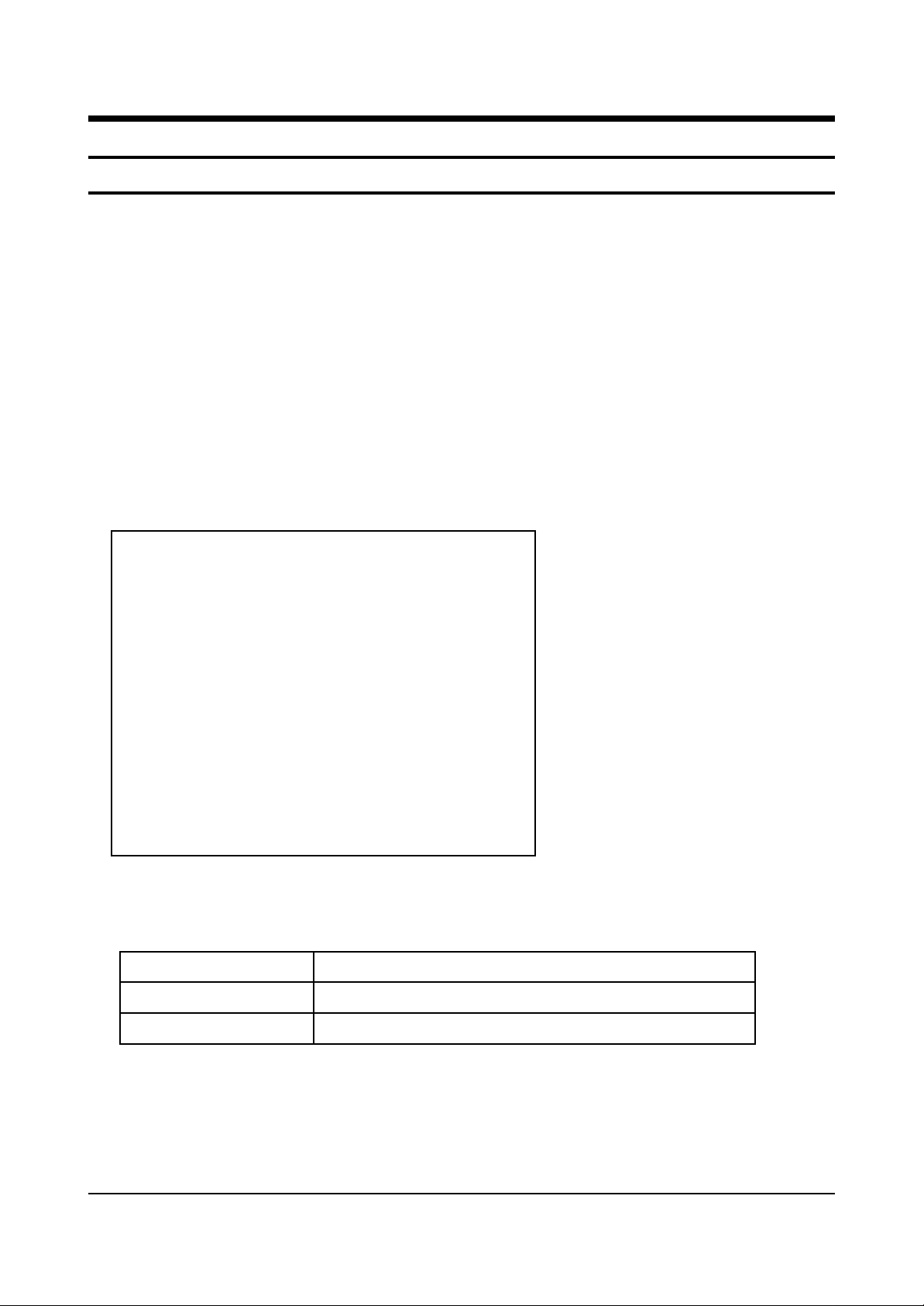
2-1-1 SERVICE MODE Entry Method (General Transmitter)
■ For the General Transmitter
1. Turn the power off and set to stand-by mode.
2. Press the buttons of the transmitter in this order; Info-Menu-Mute-Power to turn the set on.
3. The set turns on and enters service mode.
* If you fail to enter service mode, repeat steps 1 and 2 above.
2-1-2 Initial DISPLAY State of SERVICE MODE
2-1-2(A) OSD DISPLAY
2-1-2(B) B
utton Operations in SERVICE MODE
1. VSP9437-1 9. CXA2101
2. VSP9437-2 10. LOSIC
3. FLI2300 11. TP LOG-ASI
4. ASI500-1 12. Option
5. ASI500-2 13. CheckSum 0000
6. DNIe 14. Reset
7. AD9888
8. CXA2151
Release : 2003-05-02 M_NNWS42M6_100
Menu
UP/DOWN Key
LEFT/RIGHT Key
Displays all menus
Cursor move to select items
Enable to increase and decrease the data of the selected items
SERVICE MAIN
Page 2
Alignment and Adjustments
2-2 Samsung Electronics
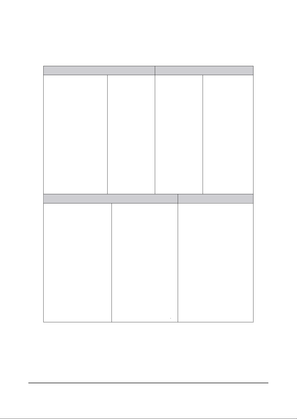
2-1-3 Factory Data Initial Value
VSP9437- 1 ( VI DEO)
V PEAKING 16
HPLL SPEED 00
RGB/YUV CONTRAST 35
RGB/YUV BRIGHTNESS 00
YUV SATCB 26
YUV SATCR 26
PAL B/G 01
PAL D/K 01
PAL I 01
SECAMB/G 27
SECAMD/K 27
SECAML'/L 27
NTSC M 01
NTSC 4.43 27
ASI500I VIDEO / PC,DVI )
R CONTRAST 32/30
G CONTRAST 32/30
B CONTRAST 32/30
R BRIGHTNESS 00
G BRIGHTNESS 00
B BRIGHTNESS 00
TEXT ALPHA 01
TEXT THRESHOLD 07
FILT ER ML 00
FILT ER MR 00
FILT ER FR 00
FILT ER MC 16
FILT ER UC 00
FILT ER LC 00
PAL 60 27
PAL M/N 01
PAL 01
SECAM 27
NTSC 01
NTSC 4.43 27
PAL 60 27
NR 01
FILTER YPASS 00
R GAMMA 32
G GAMMA 32
B GAMMA 32
H POSITION 00
V POSITION 00
HSIZE 00
VSIZE 00
OVERSCAN R 50
OVERSCAN G 50
OVERSCAN B 50
VSP9437 -2
V PEAKING 16
HPLL SPEED 01
PAL 01
SECAM 27
NTSC 01
PAL AV 01
SECAMAV 27
NTSC AV 01
PIP R CONTRAST 32
PIP G CONTRAST 32
PIP B CONTRAST 32
PIP R BRIGHTNESS 00
PIP G BRIGHTNESS 00
PIP B BRIGHTNESS 00
PIP FILTER IC 00
PIP FILTER ML 00
PIP FILTER MR 00
PIP FILTER UC 00
F LI2300
Y DELAY 05
C DELAY 12
CONTRAST 90
BRIGHTNESS 185
SATURATION 110
ASI 500 II
Page 3
Alignment and Adjustments
Samsung Electronics 2-3
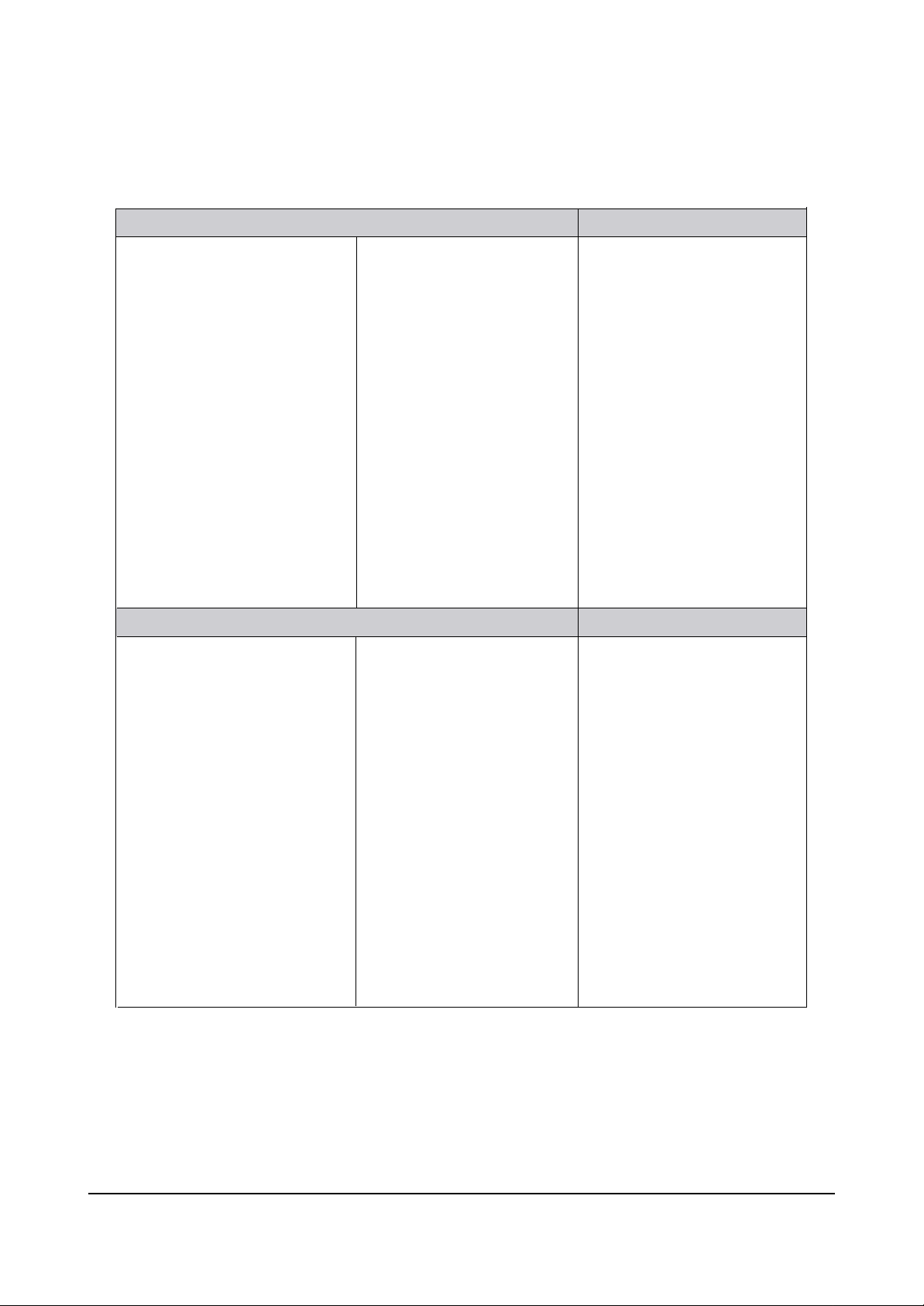
DNIe (V IDEO / PC, DVI)
BRIGHT OFFSET
CONTRA OFFSET
Attachment
Attachment
NR SCALE MAX 64
NR SCALE MIN 18
DE GAIN COR 03
DE GAIN CLIP 60/90
CE UPPER 240
CE CUTOFF 64
CE GAIN 48
W TE Y THRE 230
RCTL 02
SYNC MODE 01
PATT SEL 01
RED CONPENSA 616
CXA2 101 ( VIDEO / COMP)
PICTURE 20/20
HUE 31/31
COLOR 16/16
BRIGHT 61/61
SHARPNESS 16/16
R-DRIVE 04/04
G-DRIVE 04/04
B-DRIVE 04/04
R-CUTOFF 32/32
G-CUTOFF 32/32
B-CUTOFF 32/32
BLUE CONPENSA 616
W TE GAIN 58
RAST VSIZE 1023
RAST HSIZE 895
SHARP OFFSET 40
CLK DLY 16
H_PO SI 28
SUB-BRIGHT 32/3 2
CR-OFFSET1 07/0 7
CB-OFFSET1 07/0 7
SUB-CONT 08/06
SUB-COL 08/0 8
SUB-HUE 08/0 8
R-Y/R 13/13
R-Y/B 15/1 5
G-Y/ R 12/1 2
G-Y/ B 04/04
AD9888 (VID EO / COMP/ PC)
R GAIN 71/128/83
G GAIN 77/122/ 81
B GAIN 95/128/ 81
R, CR OFFSET 63/79/64
G, Y OFFSET 66/53/70
B, CB OFFSET 64/82/68
VIDEO PATH PC
AUTO COLOR OFF
CXA2151
GAIN SEL 01
CB GAIN 07
CR GAIN 07
YGAIN 01
HFREQ 00
Page 4

Alignment and Adjustments
2-4 Samsung Electronics
LOGIC (PDP DRIVER)
R DRIVE
G DRIVE
B DRIVE
R CUTOFF
G CUTOFF
B CUTOFF
Attachment
Attachment
Attachment
Attachment
Attachment
Attachment
GAMMA 01
GTS SET 01
ERD MODE 02
RANDOM NOISE 00
DIFF FI LTER 01
APC 01
APC SET 00
APC VALUE 127
TP LOG- ASI (TEST PAT LOGIC /SCALER)
LOG PATTERN 00
LOG HIGH LEVEL 00
LOG LOWLEVEL 00
ASI COLORBAR 00
ACTIVE V POS 12
ACTIVE H POS 19
V SYNC POS 03
H SYNC POS 32
V SYNC WIDTH 02
H SYNC WIDTH 12
OPTION
PIXEL SHIFT V
SHIFT TEST OFF
PIXEL NMBER 02
SHIFT LINE 04
SHIFT TIME 04
RGB DNIe ON
DNIe DEMO OFF
DNIe THROUGH OFF
VIDEO MUTE 00
OPTION 11 00
MDC ENABLE OFF
LAST MEMORY ON
Attachment
■
W/B Data
IC
ITEM
Video,S-VHS Component PC DVI
Bright 249 13 3 255
SNI
Contrast 240 6 249 0
R Gain 166 151 140 151
G Gain 130 130 130 130
Logic
B Gain 124 113 110 111
R Cutoff 255 255 0 02
GCutoff 0 0 0 0
BCutoff 255 0 0 02
Page 5

Alignment and Adjustments
Samsung Electronics 2-5
Alignment and Adjustments
2-2 WHITE Balance Coordinates
2-2-1 White Balance Adjustment
1. W/B Adjustment is required for the following four modes: DVI → DTV → PC → CVBS(VIDEO)
→ CVBS(VIDEO PIP)
2. Adjustment Method (DVI, DTV, PC : VG828, CVBS : Adjust RF signals to match the
Toshiba pattern (in-house signal)
! Adjust the target set by adjusting the panel logic and the video DNIe adjustment register in
register in order to determine the referential W/B of the panel with a DVI input, which
is the full digital path.
@ For DTV adjustment, adjust the adjustment register of ad9888 to align the DTV signal
to the DNIe and logic panel value which was fixed with a DVI adjustment so that they are
in effect considered to be the same signals. (At this time, do not adjust the gain of
AD9888
→ the Highlight W/B does not need to be adjusted since its deviation falls
within valid distribution range.)
# PC adjustment is same as DTV adjustment. (The offset can be applied to the values
obtained through DTV adjustment. However, additional adjustment is required for
Y, Cb, and Cr of DTV since PC processes R, G, and B signals.)
$ cvbs adjustment is performed with the Toshiba pattern (in-house signal) and differs
from the VG828 signals in the above three modes. Hence, it should be performed with
the same method of ! DVI adjustment.
% Finally, activate PIP in video mode, and repeat W/B adjustment.
❈ Thus, Micom saves the W/B data separately for each memory mode of the block
(See the block diagram given below) during W/B adjustment.
Micom can memorize the four modes
separately. However, under the current
adjustment guidelines, DTV and PC are
memorized with the same value during
DVI adjustment and CVBS is memorized
with a separate value.
Page 6

Alignment and Adjustments
2-6 Samsung Electronics
2-2-2 White Balance Coordinates by Mode
PedestalLevel Low Light
measure point
DVI
DTV COMPONENT
(480P, 720P,1080i
x 285 285 285 285
H/L
y 295
Y(fL) 36.5 21.0 37
34
295 295 295
x 285 285 285 285
L/L
y 300 300 300 295
Y(fL) 1.0 1.0 0.9 1.2
Pattern Used in Adjustment : 10 Steps Gray scalep attern
High Light
measure point
)
PC VIDEO
Page 7

Alignment and Adjustments
Samsung Electronics 2-7
2-3 Voltage Adjustment
Turning the variable resistor(VR) adjusts voltage.
T:TestPoint
VR: Variable Resistor
SMPS
CN805
CN806
CN812
T(VS)
VR4
VSET
T(VSCAN)
T(VSET)
T(VA)
T(VG)
VR3
D5V
VR6
VSCAN
VR1
VS
T(STB_5V)
CN801
VR7
VA
CN802
VR5
VE
CN803
OUTPUT Voltage(V)
VA
VSCAN(VSC)
VS
VE
See the labels attached
on the base chassis.
VR2
Vstb
T(VE)
CN804
CN800S
VSET
D5V
STB_5V
VG
+5V
+5V
+15V
Page 8

Alignment and Adjustments
2-8 Samsung Electronics
MEMO
 Loading...