

Page 1
PLASMA DISPLAY TV CONTENTS
1. Precaution
2. Product Specification
3. Disassembly & Reassembly
4. Troubleshooting
5. Exploded View & Part List
6. Wiring Diagram
SERVICE
Manual
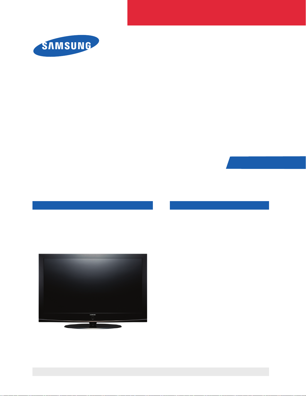
PN42A410C1D
PLASMA DISPLAY TV
Chassis : F45A(N_HD)_Carnelian
Model : PN42A410C1DXZC
Refer to the service manual in the GSPN (see the rear cover) for the more information.
Page 2
This Service Manual is a property of Samsung Electronics Co.,Ltd.
Any unauthorized use of Manual can be punished under applicable
International and/or domestic law.
© Samsung Electronics Co., Ltd. Apr. 2008
Printed in Korea
AA82-05288A
Area Web Site
North America service.samsungportal.com
Latin America latin.samsungportal.com
CIS cis.samsungportal.com
Europe europe.samsungportal.com
China china.samsungportal.com
Asia asia.samsungportal.com
Mideast & Africa mea.samsungportal.com
GSPN (Global Service Partner Network)
Page 3

Table of Contents
Chapter 1 Precaution
■ 1-1 Safety Precautions . . . . . . . . . . . . . . . . . . . . . . . . . . . . . . . . . . . . . . . . . . . . . . . . . . . . . . . . . . . 1-1
■ 1-2 Servicing Precautions . . . . . . . . . . . . . . . . . . . . . . . . . . . . . . . . . . . . . . . . . . . . . . . . . . . . . . . . 1-3
■ 1-3 Static Electricity Precautions . . . . . . . . . . . . . . . . . . . . . . . . . . . . . . . . . . . . . . . . . . . . . . . . . . . 1-4
■ 1-4 Installation Precautions . . . . . . . . . . . . . . . . . . . . . . . . . . . . . . . . . . . . . . . . . . . . . . . . . . . . . . . 1-5
Chapter 2 Product Specification
■ 2-1 Product Specification . . . . . . . . . . . . . . . . . . . . . . . . . . . . . . . . . . . . . . . . . . . . . . . . . . . . . . . . . 2-1
■ 2-2 Specifications Analysis . . . . . . . . . . . . . . . . . . . . . . . . . . . . . . . . . . . . . . . . . . . . . . . . . . . . . . . . 2-2
■ 2-3 Accessories . . . . . . . . . . . . . . . . . . . . . . . . . . . . . . . . . . . . . . . . . . . . . . . . . . . . . . . . . . . . . . . . 2-3
Chapter 3 Disassembly & Reassembly
■ 3-1 Overall Disassembly & Reassembly . . . . . . . . . . . . . . . . . . . . . . . . . . . . . . . . . . . . . . . . . . . . . 3-1
Chapter 4 Troubleshooting
■ 4-1 Troubleshooting . . . . . . . . . . . . . . . . . . . . . . . . . . . . . . . . . . . . . . . . . . . . . . . . . . . . . . . . . . . . . 4-1
■ 4-2 Adjustment . . . . . . . . . . . . . . . . . . . . . . . . . . . . . . . . . . . . . . . . . . . . . . . . . . . . . . . . . . . . . . . . . 4-16
■ 4-3 Upgrade . . . . . . . . . . . . . . . . . . . . . . . . . . . . . . . . . . . . . . . . . . . . . . . . . . . . . . . . . . . . . . . . . . . 4-32
Chapter 5 Exploded View & Part List
■ 5-1 PN42A410C1DXZC Exploded View . . . . . . . . . . . . . . . . . . . . . . . . . . . . . . . . . . . . . . . . . . . . . . 5-1
■ 5-2 PN42A410C1DXZC Service Item . . . . . . . . . . . . . . . . . . . . . . . . . . . . . . . . . . . . . . . . . . . . . . . . 5-3
Chapter 6 Wiring Diagram
■ 6-1 Overall Wiring . . . . . . . . . . . . . . . . . . . . . . . . . . . . . . . . . . . . . . . . . . . . . . . . . . . . . . . . . . . . . . . 6-1
Page 4
Product Specification
Samsung Electronics 2-1
2. Product Specification
2-1 Product Specification
Features
Block Specification Major IC Remark
RF Digital/Analog (DTV Built In)
NTSC/VSB/QAM Tuner
KS1411
PDP Module Samsung SDI W3 Module 42"HD/50"HD New Module
Power
Samsung/Dong-yang electro
mechanics SMPS
Video
NTSC 3.58, ATSC
HDMI
DNIe(FBE3)
Component, PC
SEMS10(MSD2248AL)
Sound SRS TruSuround XT, Dolby Digital SEMS10(MSD2248AL), STA335W Optical Output
Cabinet C9 Design
Specification
Model PN42A410C1D PN50A410C1D
Screen Size 42 Inches (16:9) 50 Inches (16:9)
Dimensions (WxHxD)
41.5 x 26.3 x 3.7 inches (without stand)
41.5 x 28.5 x 12.4 inches (with stand)
48.4 x 29.8 x 3.7 inches (without stand)
48.4 x 32.0 x 12.4 inches (with stand)
Weight
59.31 lbs (without stand)
67.24 lbs (with stand)
75.41 lbs without stand
81.57 lbs with stand
PC Resolution 1024 x 768 @ 60Hz 1360 x 768 @ 60Hz
Power consumption 330W 470W
Voltage AC 100~240V, 60Hz
ANTENNA input
ANT AIR IN or CABLE IN
※75Ω
unbalanced
VIDEO input
AV1, AV2
S-VIDEO1
COMPONENT1 - 480i/480p/720p/1080i
COMPONENT2 - 480i/480p/720p/1080i
PC
HDMI1 : 480p/720p/1080i
HDMI2(DVI Compatible) - 480p/720p/1080i
480i is not contained in HDMI EDID data.
However, it can be displayed.
AUDIO input
AV1, AV2
S-VIDEO
COMPONENT1 - 480i/480p/720p/1080i
COMPONENT2 - 480i/480p/720p/1080i
PC
DVI
Audio Output AUDIO (L/R)
Speaker Output 10W + 10W
Page 5
Product Specification
2-2 Samsung Electronics
2-2 Specifications Analysis
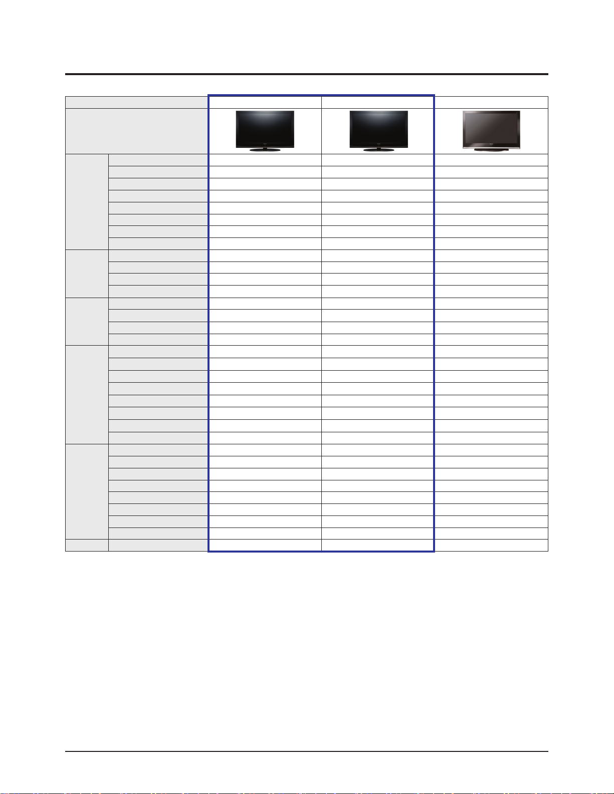
Model PN42A410C1D PN50A410C1D HP-T4254 (Lily-42HD)
Design
Basic
Display Type PDP TV PDP TV PDP TV
Built-In Tuner
○ ○ ○
Resolution 1024 x 768 1365 x 768 1024 x 768
PDP Module W3 W3 W2A
Screen Size 42" 50" 42"
Picture ratio 16 : 9 16 : 9 16 : 9
Dimensions (WxHxD) 41.5 x 28.5 x 12.4 inches 48.4 x 32.0 x 12.4 inches 41.5 x 29.9 x 12.4 inches
Weight 67.24 lbs / 30.5 kg 81.57 lbs / 37 kg 73.2 lbs / 33.2kg
Picture
Brightness 1,500 Cd/m2 1,300 Cd/m2 1,500 Cd/m2
Contrast Ratio 10000:1 10000:1 10000:1
Picture Enhacer FBE3 FBE3 FBE2
Comb Filter
○ ○ ○
Audio
Equalizer 5 Band 5 Band 5 Band
Auto Volume Control
○ ○ ○
Surround Sound SRS TruSurround XT SRS TruSurround XT SRS TruSurround XT
Speaker Output 10W + 10W 10W + 10W 10W + 10W
Features
PIP X X
○
Double Window X X
○
Caption
○ ○ ○
Still Image X X
○
EPG
○ ○ ○
My Color Control
○ ○ ○
Energy Saving
○ ○ ○
Anynet
○ ○ ○
Connections
Antenna 1(Cable or Air) 1(Cable or Air) 2 (Cable/Air)
AV Input 2 2 2
S-Video 1 1 2
Component 2 2 2
PC(D-SUB) 1 1 1
DVI X X X
HDMI 2 2 3
Optical 1 1 1
ETC Speaker/Stand Built-in Speaker Built-in Speaker Built-in Speaker
※○: application, X: non-application
Page 6
Product Specification
Samsung Electronics 2-3
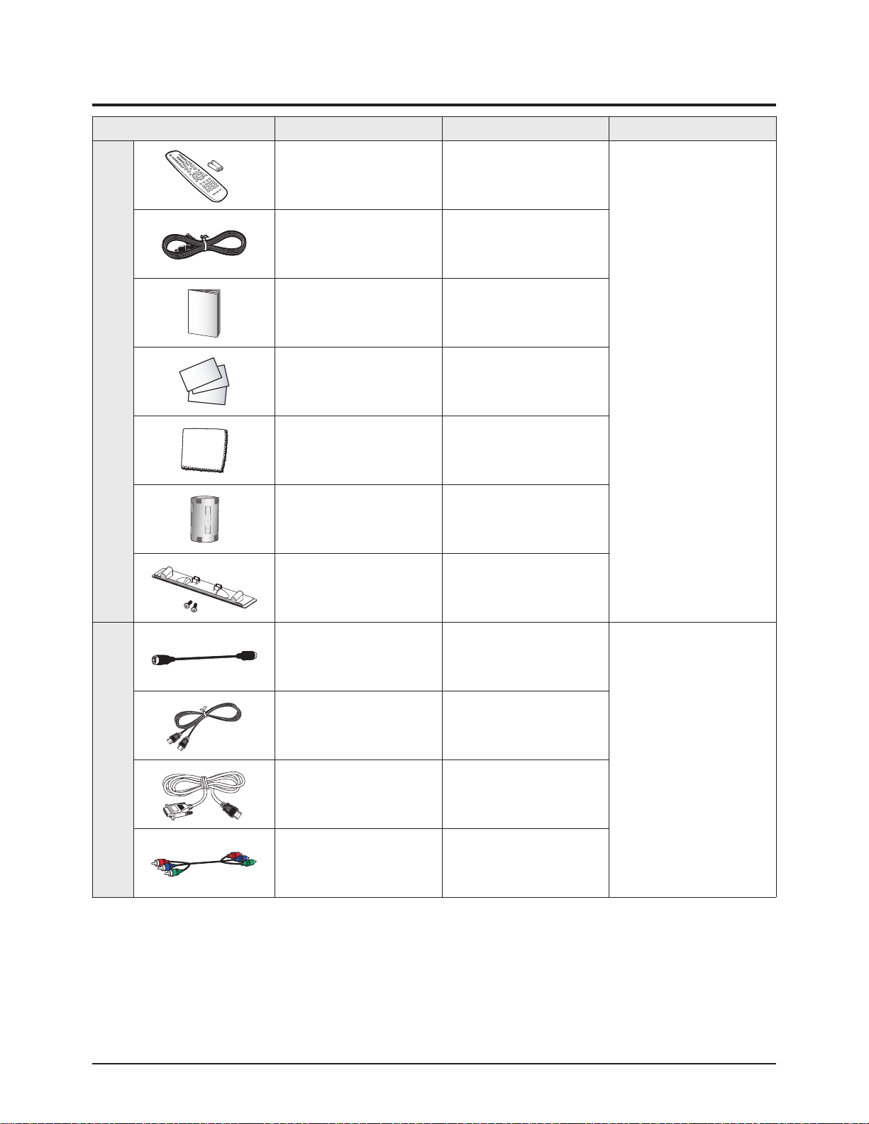
2-3 Accessories
Accessories Item Item code Remark
Supplied Accessories
Remote Control
Batteries
BN59-00678A
4301-000103
Samsung Service center
Power Cord 3903-000144
Owner's Instructions BN68-01531A
Warranty Card
Registration Card
Safety Guide Manual
AA68-00682C
-
AA68-03242L
Cloth-Clean BN63-01798A
Ferrite Core for
Power Cord
3301-001305
Cover-Bottom
Screws (2ea)
BN63-03055A
6003-001621
Accessories that can be purchased
additionally
S-VIDEO Cable
4 feet
BN39-00149A
Electronics Store/
Internal shopping mall
HDMI Cable
10 feet
BN39-00641A
HDMI/DVI cable
10 feet
BN39-00643A
Component Cables (RCA)
5 feet
BN39-00279A
Page 7
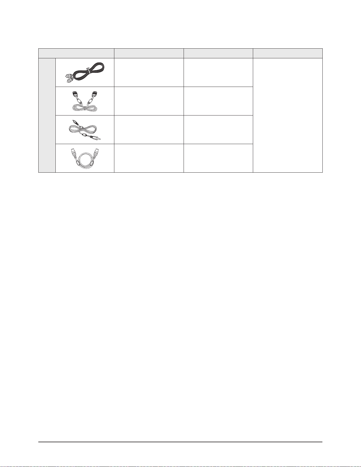
Product Specification
2-4 Samsung Electronics
Accessories Item Item code Remark
Accessories that can be purchased
additionally
Optical Cable None
Electronics Store/
Internal shopping mall
PC Cable
6 feet
BN39-00115A
PC Audio Cable
6.5 feet
BN39-00061B
Antenna Cable
10 feet
BN39-00333A
Page 8
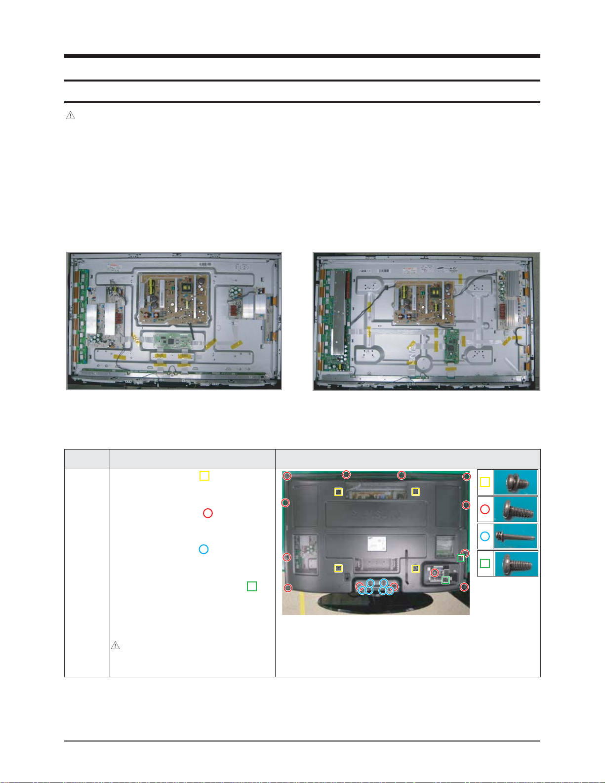
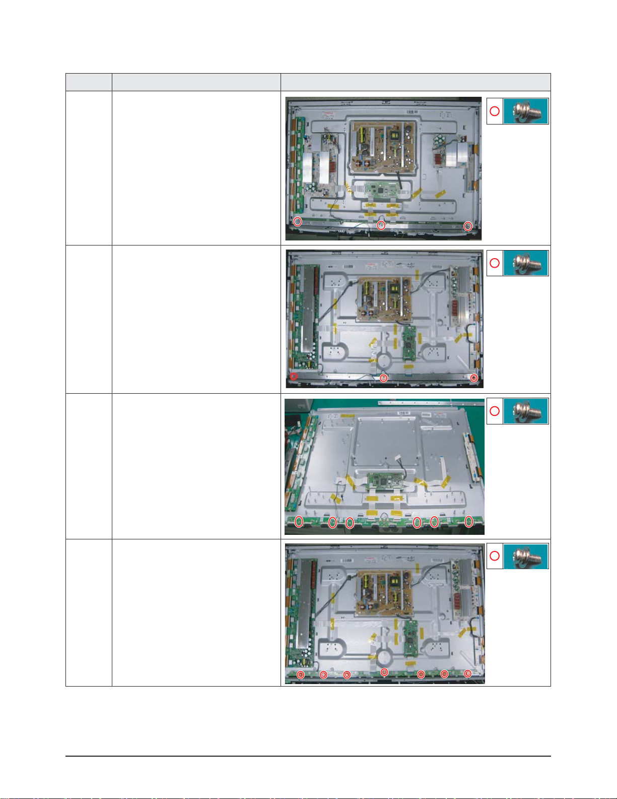
Part Name Description Description Photo
Cover
Rear
① Remove 4 screws. ( )
: M8,L16,ZPC(BLK),SWRCH18A,WP
② Remove 13 screws. ( )
: BH,+,B,M4,L3,ZPC(BLK)
③ Remove 6 screws. ( )
: PH,+,WSP,S,M4,L35,ZPC(BLK)
④ Remove the 2 machine screws. ( )
: BH,+,S,M4,L10,ZPC(BLK)
⑤ Remove the rear cover.
: Please lay the PDP unit face down on a
soft surface when removing the stand.
Disassembly & Reassembly
Samsung Electronics 3-1
3. Disassembly & Reassembly
3-1 Overall Disassembly & Reassembly
3-1-1 Separation of ASSY COVER P-REAR
Notice
- Be sure to separate the power cord before disassembling the unit.
- Discharge the capacitors first when separating PCB's with high capacity capacitors such as SMPS, X Main Board, YMain
Board, etc. (Aspark may be generated by the electric charge, and there is danger of electronic shock.)
- Check that the cables are properly connected referring to the circuit diagram when disassembling or assembling the unit
taking care not to damage the cables.
- Take care not to scratch the Glass Filter in the front.
- Assemble the boards in the reverse order of the disassembly.
- The plasma must be layed down on a flat padded surface for disassembly and reassembly.
<42">
<50">
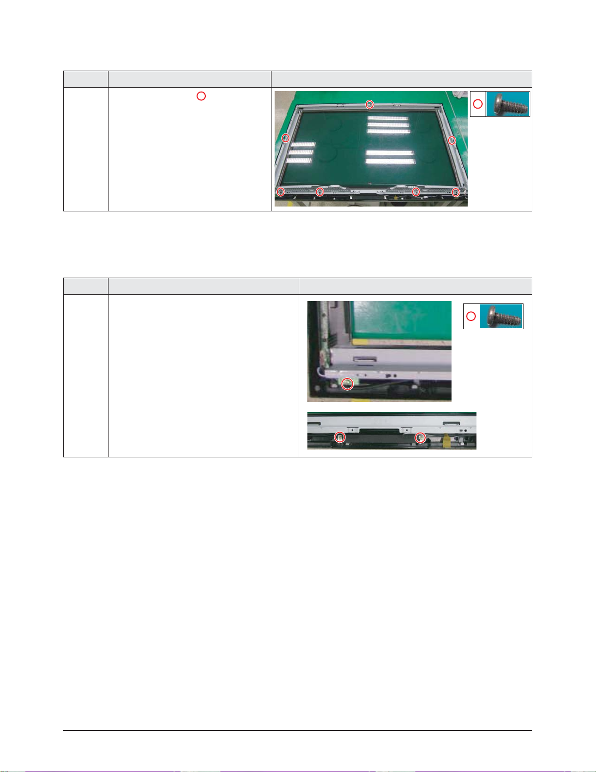
Page 9
Disassembly & Reassembly
3-2 Samsung Electronics
3-1-3 Separation of FILTER-EMI AC LINE
Part Name Description Description Photo
FILTER-
EMI
AC LINE
① Detach connector from SMPS.
② Remove 1 screws. ( )
: BH,+,S,M4,L10,ZPC(BLK)
③ Remove 2 screw. ( )
: PH,+,WWP,M3,L8,NI PLT
④ Remove screws.( )
: BH,+,S,M4,L10,ZPC(BLK)
⑤ Separate FILTER-EMI AC LINE from
bracket.
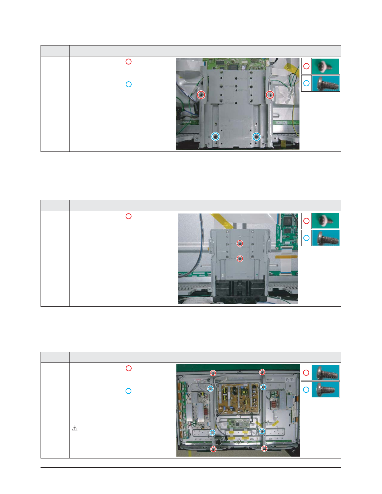
3-1-4 Separation of BRACKET-PCB
Part Name Description Description Photo
Bracket
PCB
① Remove 2 screw.( )
: BH,+,B,M4,L3,ZPC(BLK)
② Remove 2 screw.( )
: BH,+,S,M4,L10,ZPC(BLK)
③ Remove the BRACKET-PCB.
3-1-2 Separation of ASSY PCB MISC-MAIN
Part Name Description Description Photo
Main
Board
① Detach all connectors from the Main
Board.
② Remove 4 screws.
: PH,+,WWP,M3,L8,NI PLT
③ Remove the Main Board.
▶The photo is for 42".
50" is very similiar with 42".
Page 10
Disassembly & Reassembly
Samsung Electronics 3-3
3-1-7 Separation of ASSY BRACKET P-WALL
Part Name Description Description Photo
42"
Wall
Bracket
① Remove 2 screws. ( )
: BH,+,B,M4,L3,ZPC(BLK)
② Remove 6 screws. ( )
: BH,+,S,M4,L10,ZPC(BLK)
③ Remove Wall Bracket.
: Please lay the PDP panel face down
on a soft surface when separating front
cover.
3-1-5 Separation of ASSY BRACKET 42"
Part Name Description Description Photo
Bracket
① Remove 2 screws. ( )
: BH,+,PT,S Tite,M4,L10,ZPC(BLK)
② Remove 2 screws. ( )
: BH,+,B,M4,L3,ZPC(BLK)
③ Remove Bracket.
3-1-6 Separation of ASSY BRACKET 50"
Part Name Description Description Photo
Bracket
① Remove 2 screws. ( )
: BH,+,PT,S Tite,M4,L10,ZPC(BLK)
② Remove Bracket.
Page 11
Disassembly & Reassembly
3-4 Samsung Electronics
3-1-10 Separation of ASSY PDP MODULE P-LOGIC MAIN BOARD
Part Name Description Description Photo
Logic
Board
① Detach all connectors from the Logic
Main Board.
② Remove 4 screws.
: WSP,PH,+,M3,L8,NI PLT
③ Remove the Logic Main Board.
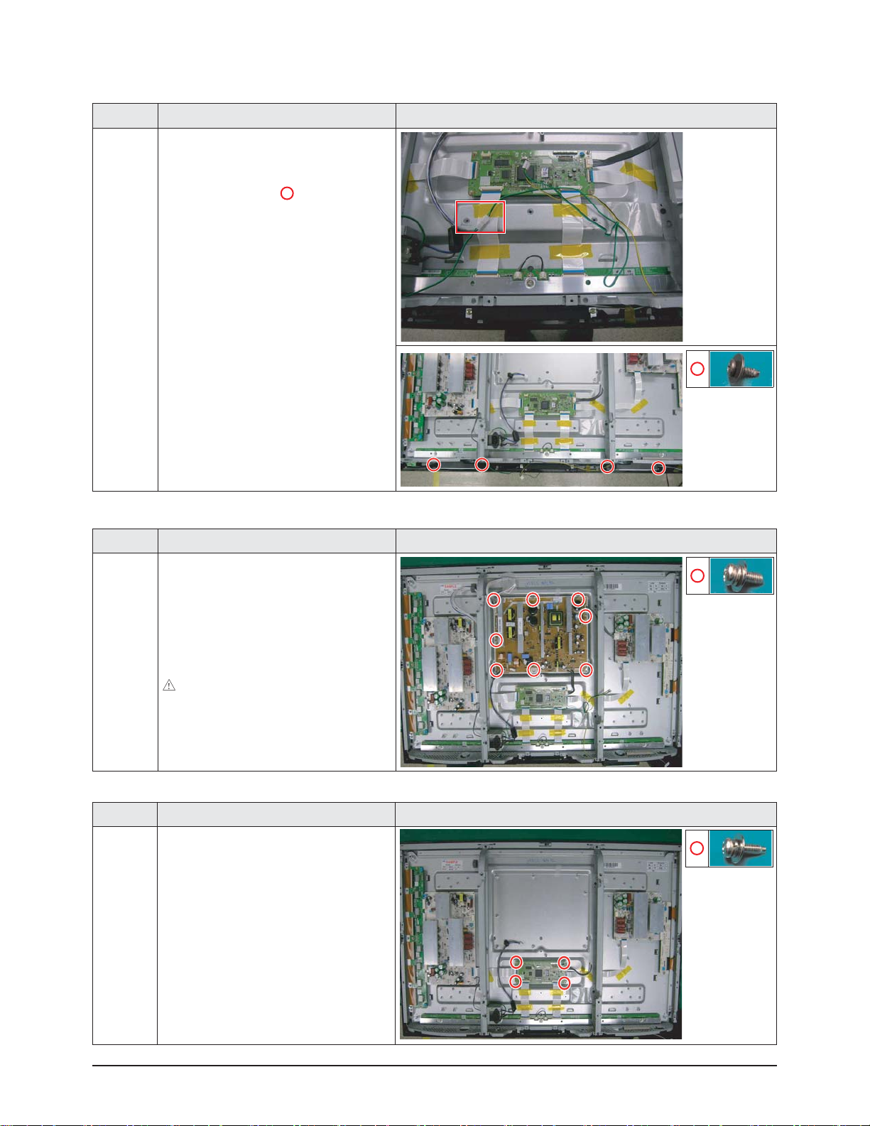
3-1-9 Separation of SMPS-PDP TV
Part Name Description Description Photo
SMPS
① Detach all connectors from the SMPS.
② Remove 8 screws.
: PH,+,WWP,M3,L8,NI PLT
③ Remove the SMPS.
: Wear gloves when handling the power
board as there may be some remaining
electrical charge in the capacitor.
Specifically, avoid touching any part of
the capacitor.
3-1-8 Separation of ASSY SPEAKER P
Part Name Description Description Photo
Speaker
① Disconnect left speaker cable from right
speaker cable.
② Remove 4 screws.( )
: BH,+,WP,B,M4.0,L3,ZPC(BLK),
SWRCH18A
③ Remove the Speaker.
▶The photo is for 42".
50" is very similiar with 42".
Page 12
Disassembly & Reassembly
Samsung Electronics 3-5
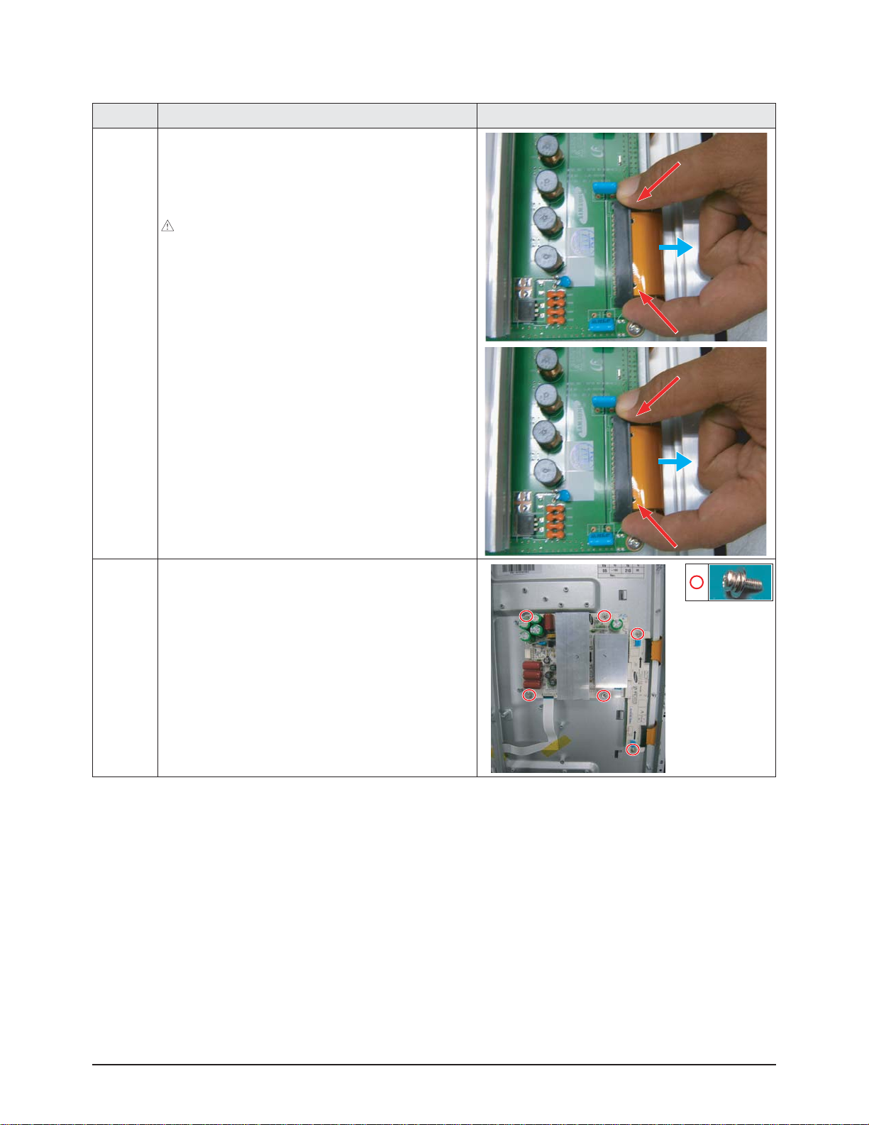
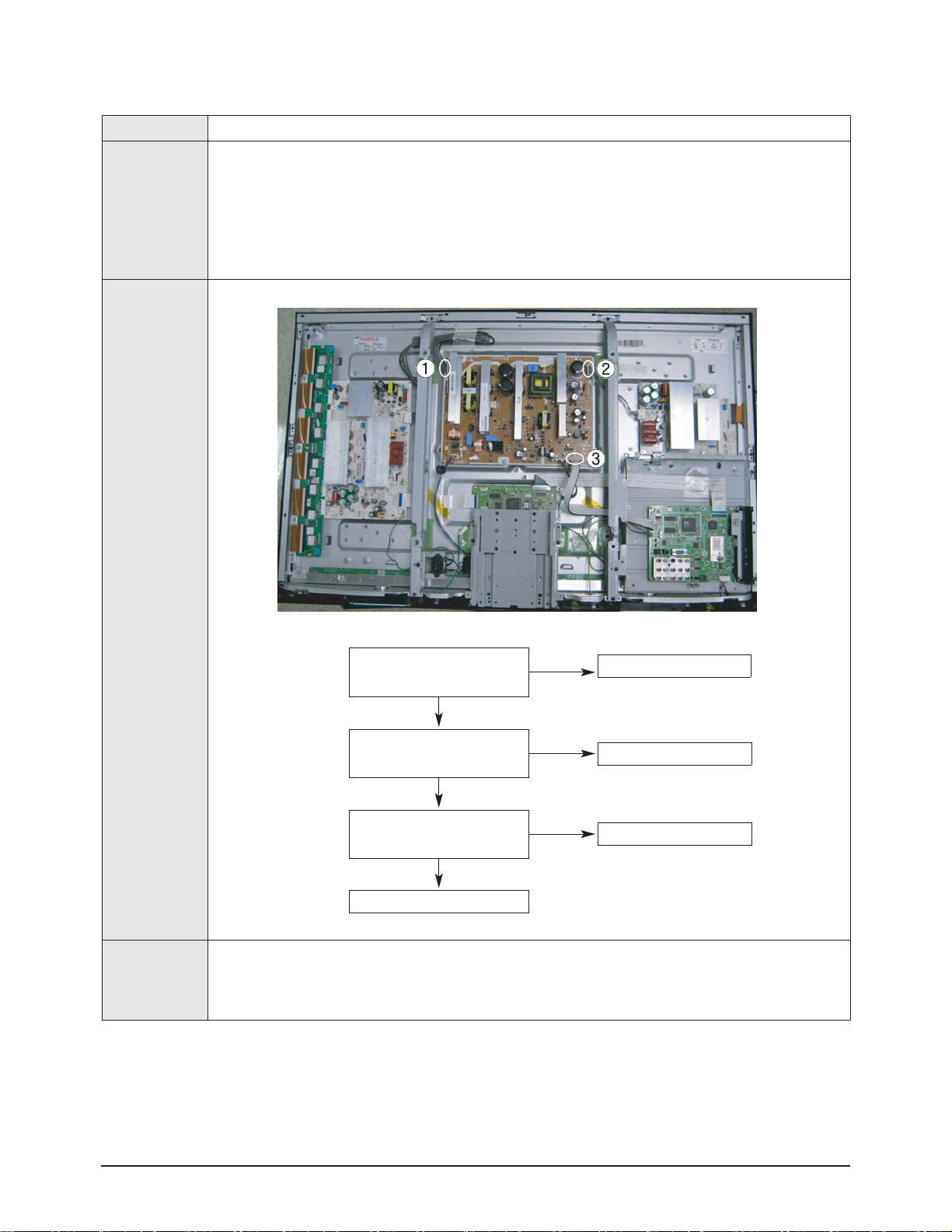
3-1-11 Separation of ASSY PDPMODULE P-X MAIN BOARD
Part Name Description Description Photo
Flat Cable
① Detach all Connectors from the X Main Board.
※ To separate the Flat Cable of the X-Board, press the
upper and the lower sides of the connector.
: Pinch the sides, but then push down in the ribbon, it
should slide out after that.
X-Main
Board
① Remove 6 screws.
: PH,+,WWP,M3,L8,NI PLT
② Remove the X-Main Board.
Page 13
Disassembly & Reassembly
3-6 Samsung Electronics
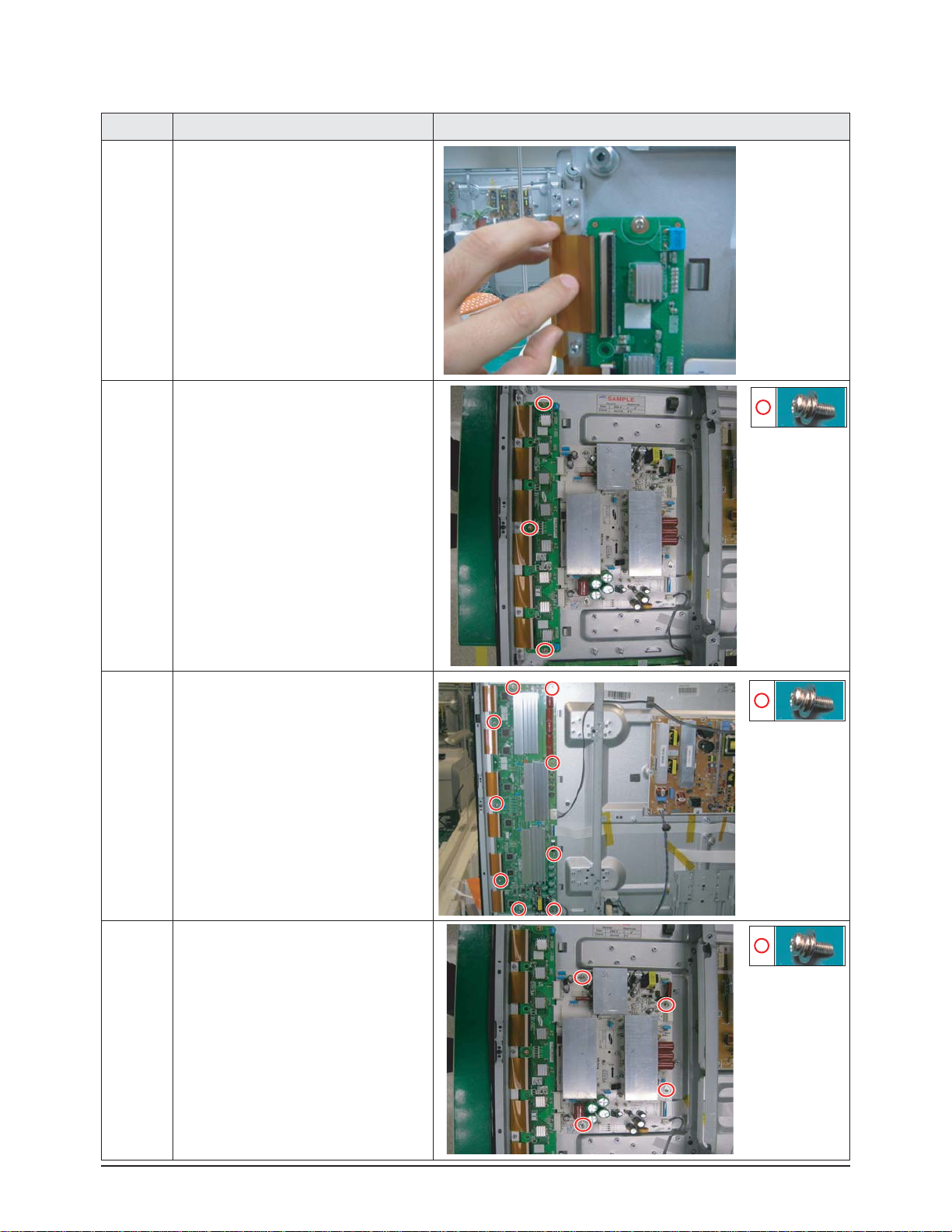
3-1-12 Separation of ASSY PDP MODULE P-Y MAIN BOARD
Part Name Description Description Photo
Flat Cable
① Detach the 6 scan board connectors
from the panel .
42"
Y-Scan
Board
① Remove 3 screws.
: PH,+,WWP,M3,L8,NI PLT
50"
Y-Scan
Board
① Remove 9 screws.
: PH,+,WWP,M3,L8,NI PLT
Y-Scan
Board
① Remove 4 screws.
: PH,+,WWP,M3,L8,NI PLT
② Detach all connectors from the Y-Main
Board.
▶This is only for 42".
Page 14
Disassembly & Reassembly
Samsung Electronics 3-7
3-1-13 Separation of ASSY PDP MODULE P-ADDRESS BUFFER BOARD
Part Name Description Description Photo
42"
Still Bar
① Remove 3 screws.
: PH,+,WWP,M3,L8,NI PLT
② Remove the still bar.
▶Before removing the still bar, you should
lift up the panel a little.
50"
Still Bar
① Remove 4 screws.
: PH,+,WWP,M3,L8,NI PLT
② Remove the still bar.
▶Before removing the still bar, you should
lift up the panel a little.
42"
Buffer
Board
① Detach the all connectors from the
buffer board.
② Remove 6 screws.
: PH,+,WWP,M3,L8,NI PLT
③ Remove the E-Board and F-Board.
50"
Buffer
Board
① Detach the all connectors from the
buffer board.
② Remove 7 screws.
: PH,+,WWP,M3,L8,NI PLT
③ Remove the E-Board and F-Board.
Page 15
Disassembly & Reassembly
3-8 Samsung Electronics
3-1-15 Separation of ASSY PCB FUNCTION & DECO LED
Part Name Description Description Photo
Function
Board
① Remove 3 screws.
: BH,+,B,M4,L3,ZPC(BLK)
3-1-14 Separation of ASSY PANEL BRACKETS
Part Name Description Description Photo
Panel
Brackets
① Remove 7 screws. ( )
: BH,+,B,M4,L3,ZPC(BLK)
② Remove the Side Panel Brackets.
Page 16

Troubleshooting
Samsung Electronics 4-1
4-1-1 First Checklist for Troubleshooting
1. Check the various cable connections first.
- Check to see if there is a burnt or damaged cable.
- Check to see if there is a disconnected or loose cable connection.
- Check to see if the cables are connected according to the connection diagram.
2. Check the power input to the Main Board.
3. Check the voltage in and out between the SMPS ↔ Main Board, between the SMPS ↔ X, YMain Board, and between the
Logic Boards.
4. Troubleshooting
4-1 Troubleshooting
Page 17
Troubleshooting
4-2 Samsung Electronics
4-1-2 Checkpoints by Error Mode
■
■
No Power
Symptom
- The LEDs on the front panel do not work when connecting the power cord.
- The SMPS relay does not work when connecting the power cord.
- The units appears to be dead.
Major Checklist
The SMPS relay or the LEDs on the front panel does not work when connecting the power cord if the cables
are improperly connected or the Main Board or SMPS is not functioning. In this case, check the following:
- Check the internal cable connection status inside the unit.
- Check the fuses of each part.
- Check the output voltage of SMPS.
- Replace the Main Board.
Troubleshooting
Procedures
Is the AC IN socket connector and
the SMPS CN800S connected?
Insert the AC in connector and the
SMPS CN800S connector
Is the Fuse (F801S) of the SMPS
Power Input Part blown?
Replace Fuse (F801S)
Replace the SMPS
SMPS CN801
Pin 3 : STB 5V
Pin 2 PS-ON : Check to see if it is 0V
Replace the Main Board
①
①
②
Yes
No
Yes
No
No
Yes
<42" (50 inches' flowchart is same with 42 inches' one)>
Page 18
Troubleshooting
Samsung Electronics 4-3
■
■
When the unit is repeatedly turned on and off
Symptom - The SMPS relay is repeatedly turned on and off.
Major Checklist
In general, the SMPS relay repeatedly turns on and off by the protection function due to a defect on a board
connected to the SMPS.
- Disconnect all cables from the SMPS, operate the SMPS alone and check if the SMPS works properly and if
each voltage output is correct.
- If the symptom continues even when SMPS is operated alone, replace the SMPS.
- If the symptom is not observed when operating the SMPS alone, find any defective assemblies by connecting
the cables one by one.
Troubleshooting
Procedures
Caution
When separating and connecting the cables such as CN810, CN809, CN808, CN807 of the Main SMPS, CN4701
of the X Main Board, and CN5707 of the Y Main Board, a spark may be generated by the electric charge of the
high capacity capacitor. Therefore, wait some time after disconnecting the power cord from the unit.
Does the symptom continue when
connecting the power after removing
CN810 from the SMPS?
Replace the Y Main Board
Does the symptom continue when
connecting the power after removing
CN809 from the SMPS?
Replace the X Main Board
Replace the Logic Board
Does the symptom continue when
connecting the power after removing
CN807 from the SMPS?
Replace the SMPS
①
②
③
Yes
No
No
No
Yes
Yes
<42" (50 inches' flowchart is same with 42 inches' one)>
Page 19

Troubleshooting
4-4 Samsung Electronics
■
■
No Picture (When audio is normal)
Symptom - Audio is normal but no picture is displayed on the screen.
Major Checklist
- This may happen when the Main Board is functioning but the X, YMain Board, Logic Board, or Y Buffer
Boards are not.
- The output voltage of the Main SMPS.
- This may happen when the LVDS cable connecting the Main Board and the Logic Board is disconnected.
Troubleshooting
Procedures
Caution
When separating and connecting the cables such as CN810, CN809, CN807 of the Main SMPS, CN4701 of the
X Main Board, and CN5707 of the Y Main Board, a spark may be generated by the electric charge of the high
capacity capacitor. Therefore, wait some time after disconnecting the power cord from the unit.
CN810
CN809
CN807
Are the Vs and Va voltages normal after
removing all cables from the SMPS?
(CN810, CN809, CN807)
Replace the SMPS
Yes
No
Did problem improve?
Did problem improve?
Did problem improve?
Did problem improve?
Replace the Y Main Board
Replace the X Main Board
Replace the Logic Board
Replace the Y Scan Board
No
No
No
No
Yes
Yes
Yes
<42" (50 inches' flowchart is same with 42 inches' one)>
Page 20

Troubleshooting
Samsung Electronics 4-5
■■
No Sound
Symptom - Video is normal but there is no sound.
Major Checklist
- When the speaker connectors are disconnected or damaged.
- When the sound processing part of the Main Board is not functioning.
- Speaker defect.
Troubleshooting
Procedures
Is the cable connection between the
Main Board and the speaker
properly connected?
Connect the cable properly or
replace the cable, if necessary.
Is the output voltage of SMPS normal?
(CN801 #13)
Replace the SMPS
Replace the Main Board
Is the speaker output terminal
of the Main Board normal?
Replace the Speaker
①
②
③
Yes
No
No
No
Yes
Yes
<42" (50 inches' flowchart is same with 42 inches' one)>
Page 21

Troubleshooting
4-6 Samsung Electronics
■
■
No Video
Symptom - Anormal/cable network analog broadcast screen is blank or abnormal but OSD is OK.
Major Checklist
- Check the antenna connection settings (Air: NTSC / ATSC, Cable: NTSC)
- Check the CVBS cable connection.
- Check the power input of the Main board.
Troubleshooting
Procedures
Is the antenna connection setting
properly configured?
Configure properly
Replace the SMPS
Check CN1001 pin2 for +5V
Replace the Main Board
①
No
No
Yes
Yes
Page 22

Troubleshooting
Samsung Electronics 4-7
■
SMPS Troubleshooting
Power ON
STBY
Abnormal
Check the UB801, DX807
Normal
Abnormal
Multi
Check the UB801, DX806, DX809
Normal
Abnormal
ྛ
VS/VA
Check the U804, DS823, DS824, DS825
Check the Other board (Image Board or Driver Board) or Cable.
Page 23

Troubleshooting
4-8 Samsung Electronics
Condition Name Description Related Board
No Voltage Output Operating Voltage don't exist PSU
No Display Operating Voltage exist, but an Image doesn't exist on screen Y-MAIN, X-MAIN, Logic Main, Cable
Abnormal Display Abnormal Image (not open or short) is no screen Y-MAIN, X-MAIN, Logic Main
Sustain Open Some horizontal lines don't exist on screen Scan Buffer, FPC of X/Y
Sustain Short Some horizontal lines appear to be linked on screen Scan Buffer, FPC of X/Y
Address Open Some vertical lines don't exist on screen Logic Main, Logic Buffer, TCP
Address Short Some vertical lines appear to be linked on screen Logic Main, Logic Buffer, TCP
■
■
Drive Board Troubleshooting
1) Troubleshooting Summary
Page 24

Troubleshooting
Samsung Electronics 4-9
2) Troubleshooting Procedure in Abnormal Conditions
① No Display
▶ No Display is related with Y-MAIN, X-MAIN, Logic Main and so on.
This page shows you how to check the boards, and the following pages show you how to find the defective board.
No Display
[ Logic Main ]
LED Blinks
Check the LED
YES NO
Check if internal is
Check if any address
data output is detected
Default Black
[ Y-MAIN ]
Check necessary points
[ Logic Main ]
Check if power is supplied
YES NO
operation
MICOM operation
Check the ASIC
Control Signal output
Check if the data
and control signals
between DDR & ASIC
( 5V, 3.3V )
Check the
are normal
[ X-MAIN ]
Check necessary points
Check the
power connectivity
Check the FUSE
Check the
input voltage
If the input voltage is
abnormal, replace the
PSU and check it
again as this indicates
a PSU output error
[ X-MAIN ]
Check several points
FUSE
OK
FET/
DIODE
OK
X-MAIN
Normal State
OPEN
Replace the Board
SHORT
Replace the Board
F5000 for VDD
F5801 for Vs
F5800 for VCC
Q5500, Q5200,
Q5201, Q5202,
Q5203, Q5400,
Q5401, Q5402,
Q5300, D5105
D5104, D5103,
Q5101, D5101,
Q5100
[ Y-MAIN ]
Check several points
FUSE
OK
FET/
DIODE
OK
Y-MAIN
Normal State
OPEN
SHORT
Replace the Board
Replace the Board
F4001 for VCC
F4003 for Vs
F4005 for VDD
F4004 for Ve
Q4002, Q4202,
Q4004, D4014,
D4013, Q4003
Q4101, Q4001,
D4018, Q4007,
Q4006, Q4005
D4011, D4004
Page 25

Troubleshooting
4-10 Samsung Electronics
② Abnormal Display(Abnormal Image is on Screen.(except abnormality in Sustain or Address))
▶ Abnormal Display is related with Y-MAIN, X-MAIN, Logic Main and so on.
This page shows you how to check the boards, and the following pages show you how to find the defective board.
Abnormal
Display
F5000 for VDD
F5801 for Vs
F5800 for VCC
[ Logic Main ]
LED Blinks
( action of Vsync )
YES
Replace the Board
[ Y-MAIN ]
Check several points
FUSE
OK
[ Logic Main ]
Observation of
abnormal display
Regular
abnormal
pattern
OPEN
Check necessary points
NO
Replace the Board
[ Y-MAIN ]
Logic Main
Normal State
Replace Panel
F4001 for VCC
F4003 for Vs
F4005 for VDD
F4004 for Ve
[ X-MAIN ]
Check necessary points
[ X-MAIN ]
Check several points
FUSE
OK
OPEN
Replace the Board
Q5500, Q5200,
Q5201, Q5202,
Q5203, Q5400,
Q5401, Q5402,
Q5300, Q5101,
Q5100
FET
OK
Y-MAIN
Normal State
SHORT
Replace the Board
Q4002, Q4202,
Q4004, Q4003
Q4101, Q4001,
Q4007, Q4006,
Q4005
FET
OK
X-MAIN
Normal State
SHORT
Replace the Board
Page 26

Troubleshooting
Samsung Electronics 4-11
③ Sustain Open (some horizontal lines don't exist on screen)
④ Sustain Short (some horizontal lines appear to be linked on Video)
[ Y-FPC ]
Sustain Open
After Changing Y-buffer,
recheck the status
OK
Done
(Defect is from Y-buffer)
NG
Replace the Panel
There is a defect on the FPC
[ Y-FPC ]
(Discharging in unwanted Scan line)
Sustain Short
After Changing Y-buffer,
recheck the status
OK
Done
(Defect is from Y-buffer)
NG
Replace the Panel
There is a defect on the FPC
Page 27

Troubleshooting
4-12 Samsung Electronics
⑤ Address Open, Short
▶ Address Open and Short is related with Logic Main, Logic Buffer, FFC, TCP film and so on.
This page shows you how to check the boards, and the following pages show you how to find the defective board.
[ Logic Main ]
Address Open/Short
Check the LED operation
LED2011 : blink
LED2010 : on
Check if the internal mode
screen is normal
OK
Reload the data onto the
MICOM and recheck it
Check the detailed waveform
and control the signal waveform
DONE
NG
Check if a specific TCP Block
screen is displayed abnormally
OK
Check the
Video Board
Check if there is an open or
short circuit on the Buffer Board
and the Logic Main address
data output section.
Check the FFC connection status
OK
OK
NG
NG
Replace Logic Main /
Address Buffer (E or F) /
check the voltage of
C2901, C2902, C2903 is 1.25V
OK
FFC
Replace the Panel
NG
check the voltage of
U2650 pin1 is 3.3V
NG
NG
Page 28

Troubleshooting
Samsung Electronics 4-13
4-1-3 Troubleshooting
Symptom Related Image Causes and Countermeasures
Ablank vertical cell (block)
appears on the screen.
Address buffer defect
- Replace the corresponding upper/lower
buffers (E, F)
COF defect (burnt)
- Replace the module
Agreen screen appears when
the TV is turned on.
The Scale is not reseting
- Replace the Main board
The OSD box appears but there
is no text.
Incorrect program version
- Check the version of each program
- Replace the Main board
Ablank upper (or lower) block
appears on the screen.
Upper/Lower Y Buffer defect
- Replace the corresponding upper/lower
buffers (E, F)
Page 29

Troubleshooting
4-14 Samsung Electronics
Symptom Related Image Causes and Countermeasures
Either the main or sub picture
does not appear.
Replace the Main board
Avertical green line appears on
the screen.
The SMPS voltage is incorrect
- Adjust the SMPS voltage according to
the voltage printed on the module label
Dim screen (blurred in red) X-Main board defect
- Replace the X-Main board
Ablank screen appears - Replace the Y-Main board
Page 30

Troubleshooting
Samsung Electronics 4-15
4-1-4 Troubleshooting Procedures by assembly
No Assembly Major Symptoms
1 SMPS-PDP TV No power, Blank screen, the Relay repeats On and Off.
2 ASSY PDP MODULE P-X-MAIN Blank screen
3 ASSY PDP MODULE P-Y-MAIN Blank screen
4 ASSY PDP MODULE P-LOGIC MAIN Blank screen, Screen noise
5 ASSY PDP MODULE P-Y-MAIN SCAN BUFFER Row Bar screen is blank (42" Only)
6 ASSY PDP MODULE P-ADDRESS E BUFFER Corresponding Buffer Board block screen is blank.
7 ASSY PDP MODULE P-ADDRESS F BUFFER Corresponding Buffer Board block screen is blank.
8 ASSY PCB MISC-MAIN No Power, Abnormal screen for each input source, PIPscreen trouble, Sound trouble
9 ASSY BOARD P-FUNCTION The side function key does not work properly
<PDP 42”>
<PDP 50”>
Page 31

Troubleshooting
4-16 Samsung Electronics
4-2 Adjustment
4-2-1 Service Instruction
■ Before Performing After Sales Services
1. Check if the measurement and test equipment is working properly.
2. Secure sufficient work space for disassembling the product.
3. Prepare a soft pad for disassembling the product.
■ Service adjustment item after replacement of Board
<If adjustment equipment is available>
① PDP Option of Factory Mode → set the Factory Data Type item as the suitable value of relevant model.
② Adjust Calibration of Factory Mode for each mode.
③ Adjust White Balance of Factory Mode.
<If adjustment equipment is not available>
① Write down the value of HDMI White Balance of Factory Mode before replacing Board.
② PDP Option of Factory Mode → set the Factory Data Type item as the suitable value of relevant model.
③ Set the value of HDMI White Balance with the value written down before.
Page 32

Troubleshooting
Samsung Electronics 4-17
4-2-2 How to Access Service Mode
1. General Remote
To Enter: → →→→→
(Interval between key strokes: less than 3 sec)
To Exit: →
2. Factory Remote
To Enter: →→→(Interval between key strokes: less than 3 sec)
To Exit: →
Press the Factory key twice with a key stroke interval of more than 1 second (Pressing once enters Aging Mode)
3. Settings when entering Factory mode
- Sharp Screen (Dynamic), Color Tone (Cool1), Factory (Dynamic CE Off), DNIe(Off)
4. Adjustment Procedures
- Channel ▲▼Key: Select an item.
- Volume ◀▶ Key : Adjust the value up or down.
- MENU Key : Save the changes to the EEPROM and return to the higher-level mode.
- Using the Numeric (0~9) keys, you can select a channel.
- Using the SOURCE key, you can switch AV modes.
5. Initial SERVICE MODE DISPLAY State
※ The version of the firmware displayed at the bottom of the screen may differ and the firmware is subject to change for the
improvement of product functions.
※ If you have adjusted the settings in Service Mode, you have to reset the product.
※ If you exit Service Mode without reset, DNIe vlaue keeps Off regardless of setting up the user.
POWER OFF MUTE POWER ON
POWER OFF POWER ON
POWER OFF POWER ON
1 8 2
POWER ON INFO FACTORY Key
1. ADC
2. ADC Target
3. ADC Result
4. Option Byte
5. Adjust
6. White Balance
7. W/B Movie
8. EPAstandard
9. FBE3
10. VDEC
11. Scaler
12. Sharpness
13. PE
14. Sound
15. Dynamic Contrast
16. PDP Option
17. Expert Settings
18. Expert D-Settings
19. Expert Gray Scale
20. Expert C-Space
21. Expert Others
22. CHECKSUM 0x0000
23. Reset
T-CRLAUSC-00xx
Dec 29 2007
PN42A450
EDID FAIL
Option :
Page 33

Troubleshooting
4-18 Samsung Electronics
4-2-3 Factory Data
★★
The underlined are items applied during the service adjustment. None of the others should be adjusted.
1. ADC
Item Data
AV Calibration Comp Calibration PC Calibration HDMI Calibration -
2. ADC Target
Item Default data
1st_AV_Low 18
1st_AV_High 220
1st_AV_Delta 1
1st_COMP_Low 16
1st_COMP_High 235
1st_COMP_Delta 1
1st_PC_Low 1
1st_PC_High 235
1st_PC_Delta 1
2nd_AV_Low 1
2nd_AV_High 235
2nd_AV_Delta 1
2nd_COMP_Low 1
2nd_COMP_High 235
2nd_COMP_Delta 1
2nd_PC_Low 1
2nd_PC_High 235
2nd_PC_Delta 1
2nd_HDMI_Low 1
2nd_HDMI_High 235
2nd_HDMI_Delta 1
Page 34

Troubleshooting
Samsung Electronics 4-19
3. ADC Value
4. Option Byte
Item Default data TV/AV/S_Video Component PC DTV/HDMI Remark
LUMA_OFFSET 128 140 - - -
LUMA_GAIN 128 118 - - -
RED_CUTOFF 128 - 128 130 -
GREEN_CUTOFF 128 - 127 132 -
BLUE_OFFSET 128 - 128 128 -
RED_GAIN 128 - 105 78 -
GREEN_GAIN 128 - 105 79 -
BLUE_GAIN 128 - 105 78 2nd_R offset 128 106 110 110 112
2nd_G offset 128 108 113 110 112
2nd_B offset 128 106 111 110 112
2nd_R gain 128 128 118 128 118
2nd_G gain 128 128 117 128 118
2nd_B gain 128 1150 118 128 118
Item Default data
LCD/PDP LCD
Model Select L450
Inch 32 Inch
Panel Option 32AM
Dimming INT
Mirror OFF
AV Number 2
COMP. Number 2
HDMI Number 3
Light Effect ON
HeadPhone ON
Anynet+(HDMI-CEC) ON
Carrier Mute OFF
Volume Curve Large
RS 232C Auto wall
Gamma 0.9
Mute Time[RF] 400ms
CH Memory Samex
PC Mode Ident Auto
HDMI Mode Ident Auto
HPD Control 1200ms
Page 35

Troubleshooting
4-20 Samsung Electronics
5. Adjust
6. White Balance
Item Default data
Watchdog Enable ON
Watchdog Count 10sec
Spread Spectrum OFF
Shop Mode OFF
DEBUG MODE DEBUG OFF
MSTAR Out Format Vesa
FBE In Format Vesa
FBE Out Format Vesa
Hotel Option
EDID
HDCP Key Download
Item Default data TV/AV/S_Video Component PC DTV/HDMI Remark
Sub Brightness 128 128 128 128 128
R-Offset 128 128 128 128 128
G-Offset 128 128 128 128 128
B-Offset 128 128 128 128 128
Sub Contrast 128 128 128 128 128
R-Gain 128 128 128 128 128
G-Gain 128 128 128 128 128
B-Gain 128 128 128 128 128
Page 36

Troubleshooting
Samsung Electronics 4-21
7. W/B Movie
Item Default data
W/B MOVIE Off
MODE -
Color Tone -
MSub Brightness -
MSub Contrast -
W2_Rgain -
W2_Bgain W2_Roffset W2_Boffset -
W1_Rgain -
W1_Bgain W1_Roffset W1_Boffset -
NOR_Rgain -
NOR_Bgain NOR_Roffset NOR_Boffset -
C2_Rgain -
C2_Bgain C2_Roffset C2_Boffset -
Movie Contrast -
Movie Bright Movie Color -
Movie Sharpness -
Movie Tint -
Movie Backlight -
Movie Gamma -
8. EPAStandard
Item Default data
Standard Contrast 80
Standard Brightness 45
Standard Sharpness 50
Standard Color 50
Standard Tint 0
Standard Backlight 7
Page 37

Troubleshooting
4-22 Samsung Electronics
9. FBE3
Item Default data RF
AV / SVIDEO
COMP480i/
480p
COMP720p/1
080i/1080p
HDMI DTV
HDMI PC/
Aanalog PC
Patt-Sel 0 0 0 0 0 0 0 0
B-Slope gain 60 60 60 60 60 60 60 60
B-Tilt min 30 30 30 30 30 30 30 30
B-Tilt max 110 110 110 110 110 110 110 110
Lfunc-Basis 75 75 75 75 75 75 75 75
Hfunc-Basis 80 80 80 80 80 80 80 80
Mean-Offset1 30 30 30 30 30 30 30 30
Mean-Offset2 235 235 235 235 235 235 235 235
Mean-Slope 112 112 112 112 112 112 112 112
ACR-Offset 10 10 10 10 10 10 10 10
ACR-Th1 10 10 10 10 10 10 10 10
ACR-Th2 110 110 110 110 110 110 110 110
Skin-Enable ON ON ON ON ON ON ON ON
Skin-UV 128 128 128 128 128 128 128 128
Sub color 128 128 128 128 128 128 128 128
M-Skin-UV 128 128 128 128 128 128 128 128
M-Sub color 128 128 128 128 128 128 128 128
10. VDEC
Item Default data RF AV S-VHS
Saturation 0x80 80 80 80
CTI_MD 0x02 2 2 2
CBCRLP_MD 0x01 0 0 0
11. Scaler
Item Default data
DNR_off 0
DNR_low 2
DNR_mid 3
DNR_high 4
Y_DELAY_EN 1
YC_STEP 1
Page 38

Troubleshooting
Samsung Electronics 4-23
12. Sharpness
14. Sound
Item Range
Carrier Mute 1
High DEV 0
CM_TH_HIGH 2990
CM_TH_LOW 20B0
ST_PILOT_TH_HIGH D00
ST_PILOT_TH_LOW 600
ST_VAR_TH_HIGH 1800
ST_VAR_TH_LOW 1000
SAP_AMP_TH_HIGH 1
SAP_AMP_TH_LOW 4
SAP_NSR_TH_HIGH 4500
SAP_NSR_TH_LOW 3000
"AMP_Volume" 29
Limiter Attack 9
Limiter Release F
Post Scale 7F
Speaker EQ 0
AV Sync. 3C
Item Default data RF AV/S-VHS
component HDMI DTV
PC /
HDMI pc timing
480i/p 720p1080i / p 480i/p 720p1080i / p SD HD
H1 Gain 0x10 0x10 0x10 0x10 0x10 0x10 0x10 0x10 0x10 0x10
H2 Gain 0x08 0x08 0x08 0x08 0x08 0x08 0x08 0x08 0x08 0x08
H3 Gain 0x08 0x08 0x08 0x08 0x08 0x08 0x08 0x08 0x08 0x08
H4 Gain 0x08 0x08 0x08 0x08 0x08 0x08 0x08 0x08 0x08 0x08
V1 Gain 0x28 0x28 0x28 0x28 0x28 0x28 0x28 0x28 0x28 0x28
V2 Gain 0x08 0x08 0x08 0x08 0x08 0x08 0x08 0x08 0x08 0x08
H overshoot 0xFF 0xFF 0xFF 0xFF 0xFF 0xFF 0xFF 0xFF 0xFF 0xFF
V overshoot 0x60 0x60 0x60 0x60 0x60 0x60 0x60 0x60 0x60 0x60
H undershoot 0xFF 0xFF 0xFF 0xFF 0xFF 0xFF 0xFF 0xFF 0xFF 0xFF
V undershoot 0x60 0x60 0x60 0x60 0x60 0x60 0x60 0x60 0x60 0x60
Coring TH2 0x01 0x01 0x01 0x01 0x01 0x01 0x01 0x01 0x01 0x01
Coring TH1 0x01 0x01 0x01 0x01 0x01 0x01 0x01 0x01 0x01 0x01
Mid_color_level 0xAC
13. PE
Item Default data control register 480i 480p 720p 1080i
Page 39

Troubleshooting
4-24 Samsung Electronics
15. Dynamic Contrast
Item Default data
Dynamic Contrast On
Dynamic Dimming Off
Y_MEAN 0
16. PDP Option
Item Default data control register Range Remark
Pixel Shift Test Off ON/OFF
Panel Pattern Select 0
Panel Resolution -
Panel Inch -
Panel Version -
Panel Temperature -
Logic SW Version -
Model Select P450
Factory Data Type 42SP5
Checksum -
MB SW Off
MB Offset 0xC0
Ve Signal Control 0xBFFF
FRC Mode 100Hz
FRC DBG MarkOn 0
17. Checksum
18. Reset
Page 40

Troubleshooting
Samsung Electronics 4-25
4-2-4 Service Adjustment - You must perform Calibration in the Lattice Pattern before adjusting the White Balance.
■■
Color Calibration
Adjust spec.
1. Source : HDMI
2. Setting Mode : 1280*720@60Hz
3. Pattern : Pattern #24 (Chess Pattern)
4. Use Equipment : CA210 & Master MSPG925 Generator
※ Use other equipment only after comparing the result with that of the Master equipment.
( Chess Pattern )
Input mode Calibration Pattern
CVBS IN (Model_#1) Perform in NTSC B&W Pattern #24 Lattice
Component IN (Model_#6) Perform in 720p B&W Pattern #24 Lattice
PC Analog IN (Model_#21)
Perform in VESAXGA(1024x768)
B&W Pattern #24
Lattice
HDMI IN Perform in 720p B&W Pattern #24 Lattice
<Table 1>
Page 41

Troubleshooting
4-26 Samsung Electronics
■ Method of Color Calibration (AV)
1) Apply the NTSC Lattice (N0. 3) pattern signal to the AV IN 1 port
2) Press the Source key to switch to "AV1" mode
3) Enter Service mode
4) Select the "Calibration" menu
5) Select the "AV Calibration" menu.
6) In "AV Calibration Off" status, press the "▶" key to perform Calibration.
7) When Calibration is complete, it returns to the high-level menu.
8) You can see the change of the "AV Calibration" status from Failure to Success.
■ Method of Color Calibration (Component)
1) Apply the 720p Lattice (N0. 6) pattern signal to the Component IN 1 port
2) Press the Source key to switch to "Component1" mode
3) Enter Service mode
4) Select the "Calibration" menu
5) Select the "Comp Calibration" menu.
6) In "Comp Calibration Off" status, press the "▶" key to perform Calibration.
7) When Calibration is complete, it returns to the high-level menu.
8) You can see the change of the "Comp Calibration" status from Failure to Success.
■ Method of Color Calibration (PC)
1) Apply the VESAXGA Lattice (N0. 21) pattern signal to the PC IN port
2) Press the Source key to switch to "PC" mode
3) Enter Service mode
4) Select the "Calibration" menu
5) Select the "PC Calibration" menu.
6) In "PC Calibration Off" status, press the "▶" key to perform Calibration.
7) When Calibration is complete, it returns to the high-level menu.
8) You can see the change of the "PC Calibration" status from Failure to Success.
■ Method of Color Calibration (HDMI)
1) Apply the 720p Lattice (N0. 6) pattern signal to the HDMI1/DVI IN port
2) Press the Source key to switch to "HDMI1" mode
3) Enter Service mode
4) Select the "Calibration" menu
5) Select the "HDMI Calibration" menu.
6) In "HDMI Calibration Off" status, press the "▶" key to perform Calibration.
7) When Calibration is complete, it returns to the high-level menu.
8) You can see the change of the "HDMI Calibration" status from Failure to Success.
Page 42

Troubleshooting
Samsung Electronics 4-27
■
■
White Balance
Adjust spec.
1. Source : HDMI
2. Setting Mode : 1280*720@60Hz
3. Pattern : Pattern #92
4. Use Equipment : MIK-7256 (MSPG925L)
5. Work order
① Connect HDMI (DVI) output terminal of MIK-7256 (MSPG925L) to the HDMI input in main set
② Set the input to HDMI mode
③ Enter the White Balance menu of service mode
④ Contact CA-210 sensor to glass filter
⑤ Adjust the low light
- Adjust Sub-Bright (LBE) to set the 'Y' value
- Adjust R-Offset ('x') and B-Offset ('y') to the color coordinates.
* Do not adjust G-Offset data
⑥ Adjust the high light.
- Adjust Sub-Contrast (LBE) to set the 'Y' value
- Adjust R-Gain ('x') and B-Gain ('y') to the color coordinates.
* Do not adjust the G-gain data
( SAMSUNG WHITE BALANCE Adjustment PATTERN with FPD )
( Fixed Position of CA210 Probe )
Page 43

Troubleshooting
4-28 Samsung Electronics
Input mode
(CA-210)
x Y(L) T(K), MPCD
CVBS
(NTSC)
H/L 278
FIX
10,500 (± 0)
(Sub_CT:128)
L/L 278
10.5 cd/㎡
11,000 (-3)
(3.0 Ft)
COMP
(720P)
H/L 278
FIX
10,500 (± 0)
(Sub_CT:128)
L/L 278
10.3 cd/㎡
11,000 (-6)
(3.0 Ft)
HDMI
(720P)
H/L 278
FIX
10,500 (± 0)
(Sub_CT:128)
L/L 278
10.3 cd/㎡
10,500 (± 0)
(3.0 Ft)
Page 44

Troubleshooting
Samsung Electronics 4-29
Replaced assembly items Check Items
ASSY PCB MISC-MAIN
1) Auto Program
2) White Balance Adjust
SMPS-PDP TV Vs, Va voltage check and adjust
ASSY PDP MODULE P-LOGIC MAIN
Not to be adjusted
ASSY PDP MODULE P-X-MAIN
ASSY PDP MODULE P-Y-MAIN
ASSY PDP MODULE P-Y-MAIN SCAN BUFFER
ASSY PDP MODULE P-ADDRESS E BUFFER
ASSY PDP MODULE P-ADDRESS F BUFFER
ASSY BOARD P-SIDE HDMI A/V
* PDP 50" Check items listed after changing each
Replaced assembly items Check Items
ASSY PCB MISC-MAIN
1) Auto Program
2) White Balance Adjust
SMPS-PDP TV Vs, Va voltage check and adjust
ASSY PDP MODULE P-LOGIC MAIN
Not to be adjusted
ASSY PDP MODULE P-X-MAIN
ASSY PDP MODULE P-Y-MAIN
ASSY PDP MODULE P-Y-MAIN SCAN BUFFER
ASSY PDP MODULE P-Y-MAIN SCAN BUFFER
ASSY PDP MODULE P-ADDRESS E BUFFER
ASSY PDP MODULE P-ADDRESS F BUFFER
ASSY BOARD P-SIDE HDMI A/V
※ When replacing the SMPS or PDP panel, you have to check the voltage printed on the panel sticker and adjust it.
4-2-5 Replacements & Calibration
* PDP 42" Check items listed after changing each
Page 45

Troubleshooting
4-30 Samsung Electronics
2. Apoint of adjusting SMPS-MAIN voltage.
Value Board Adjustment
Vs 210
SMPS
Va 55
Vset -
Ve 95
Vscan -190
■
Voltage Adjustment
1. After replacing the SMPS or PDPpanel, you must adjust the voltage referring to the voltage label printed on the panel.
(If you do not adjust the voltage, an abnormal discharge symptom may appear.)
SMPS
Voltage Label
Vs
Va
Page 46

Troubleshooting
Samsung Electronics 4-31
■
■
Y-RR and Y-FR controls
Set the main reset (rising : 60usec, falling : 80usec) by change the value of variable resistor.
<42">
<50">
▶The picture is only for 50".
42" has only Falling ramp variable resistor.
Test Point
60usec
Rising ramp
variable resistor
Falling ramp
80usec
variable resistor
Test Point
Page 47

Troubleshooting
4-32 Samsung Electronics
4-3 Upgrade
4-3-1 USB Download Method
1. Copy the Upgrade Files into the path "T-CRLAUSC" in USB flash driver.
2. USB Download
① Insert the USB Memory Stick to the SERVICE port in Stand-by mode.
② Turn the power on.
③ Press "MENU" and find "SW Upgrade" in Menu "SETUP".
④ Select the "SW Upgrade" from the menu.
⑤ Select "USB" from the menu.
⑥ The banner OSD "Scaning for USB..." is displayed.
⑦ The banner OSD "Upgrade version **** to version ****" is displayed.
Select "Yes".
⑧ The banner OSD "Upgrade version **** to version ****" is displayed.
It takes about 30 sec.
(Warning: Don't remove USB flash driver during upgrade.)
⑨ The banner OSD "Upgrade is completed" is displayed when the upgrade is
completed.
⑩ Remove the USB flash driver from PDP TV and check the program version.
Page 48

Troubleshooting
Samsung Electronics 4-33
4-3-2 How to Check the Version of the Program
1. Procedures for checking in the User Menu
① Select the "Setup" menu in the Menu screen
② Place the cursor over the "SW Upgrade" of "Setup" and press the "info" key on the remote control.
③ The version of the program is displayed at the bottom of the Menu screen
2. How to check Program Version on factory mode.
PROGRAM VERSION
PROGRAM VERSION
Page 49

Samsung Electronics5-1
Exploded View & Part List
5. Exploded View & Part List
5-1 PN42A410C1DXZC Exploded View
M0013
M0412
T0165
T0079
M0523
T0044
M0125
M0523
M0149
T0175
T0456
M0027
T0175
M0146
M0150
T0003
M0146
T0023
M0150
M0145
M0105
M0112
T0056
CIS7
T0023
Page 50

5-2Samsung Electronics
Exploded View & Part List
Loc. No. Code No. Description Specification Q'ty SA/SNA Remark
CIS7 AA61-60003B SPRING ETC-CS -,SUS304,-,-,OD11.2,N7,OD1 1 S.N.A
M0013 BN96-06752C ASSY COVER P-REAR P410 42Inch,PCM T0.5,B 1 S.A
M0027 BN96-05835A ASSY STAND P-BASE -,42Q9/42C9,-,ABS,SF-0 1 S.A
M0105 BN67-00190A LENS-LED 42Q9,PC,light blue,Material of 1 S.N.A
M0112 BN63-03047J COVER-FRONT P410 42,ABS,HB,BK23,STEAM MO 1 S.N.A
M0125 BN96-07190A ASSY INLET P Pyrope,350mm,IG-N06BES1,250 1 S.A
M0145 BN96-04853E ASSY BOARD P-FUNCTION Carnelian,CT5000-4 1 S.A
M0146 BN96-06750A ASSY BRACKET P-FILTER SIDE P450 42Inch,S 2 S.N.A
M0146 BN96-07666B ASSY BOARD P-POWER & IR P410 Carnelian,P 1 S.A
M0149 BN96-06749A ASSY BRACKET P-FILTER TOP P450 42Inch,SA 1 S.N.A
M0150 BN96-06751A ASSY BRACKET P-FILTER BOTTOM P450 42Inch 1 S.N.A
M0150 BN96-06748A ASSY BRACKET P-SUPPORT FILTER P410 42Inc 1 S.N.A
M0412 BN96-06697D ASSY BRACKET P-PCB 42P450,SEA,SECC,T0.5 1 S.N.A
M0523 BN96-06753A ASSY BRACKET P-SUPPORT STAND P410 42Inch 1 S.N.A
M0523 BN96-06756A ASSY BRACKET P-WALL P410 42Inch,SECC T1. 2 S.N.A
T0003 BN96-06746E ASSY COVER P-FRONT P410 42Inch,ASIA,ABS+ 1 S.A
T0023 BN96-04707A ASSY COVER P-KNOB POWER C9/Q9,,ABS HB,,, 1 S.A
T0023 BN64-00567A KNOB POWER 42Q9,PC,VIOLET 1 S.N.A
T0044 BN96-06642A ASSY PDP MODULE P PL42AX030A,42HD W3,W3, 1 S.A
T0056 BN63-03091B COVER-DECORATION 42C92,ABS,HB,BLM-1520 1 S.N.A
T0079 BN94-01795A ASSY PCB MISC-MAIN PN42A410C1DXZA,F45A 1 S.A
T0165 BN96-06696K ASSY COVER P-AV 42P450 1 S.N.A
T0175 BN96-04704D ASSY SPEAKER P 8ohm,P410 42",L350mm / R4 1 S.A
T0175 BN96-04704F ASSY SPEAKER P 8ohm,P410 42"/50" R,200m 1 S.A
T0456 BN67-00206A GLASS-EMI FILTER 42 C9, without AR,Sputt 1 S.A
Page 51

Samsung Electronics5-3
Exploded View & Part List
5-2 PN42A410C1DXZC Service Item
Loc. No. Code No. Description Specification Q'ty Remark
M0013 BN96-06752C ASSY COVER P-REAR P410 42Inch,PCM T0.5,B 1
M0027 BN96-05835A ASSY STAND P-BASE -,42Q9/42C9,-,ABS,SF-0 1
M0154 BN96-06760A ASSY PDP P-Y-MAIN BUFFER PL42AX030A,42HD 1
M2893 BN39-00827A LEAD CONNECTOR LILLY 42"/50",UL1007#26,U 1
T0003 BN96-06746E ASSY COVER P-FRONT P410 42Inch,ASIA,ABS+ 1
T0037 BN96-06761A ASSY PDP P-LOGIC MAIN PL42AX030A,42HD W3 1
T0038 BN96-06762A ASSY PDP P-ADDRESS E-BUFFER PL42AX030A,4 1
T0039 BN96-06763A ASSY PDP P-ADDRESS F-BUFFER PL42AX030A,4 1
T0044 BN96-06642A ASSY PDP MODULE P PL42AX030A,42HD W3,W3, 1
T0045 BN96-06757A ASSY PDP P-X-MAIN BOARD PL42AX030A,42HD 1
T0045 BN96-06758A ASSY PDP P-X-MAIN BUFFER PL42AX030A,42HD 1
T0074 BN59-00678A REMOCON TM-95,39,AMERICA 1
T0079 BN94-01795A ASSY PCB MISC-MAIN PN42A410C1DXZA,F45A 1
T0175 BN96-04704D ASSY SPEAKER P 8ohm,P410 42",L350mm / R4 1
T0175 BN96-04704F ASSY SPEAKER P 8ohm,P410 42"/50" R,200m 1
T0262 BN96-06759A ASSY PDP P-Y-MAIN BOARD PL42AX030A,42HD 1
T0764 BN44-00206A SMPS-PDP TV W3 PDP SMPS,SEM,AC/DC,406.6W 1
※ This is the list which is available to repair the real material at the time of service.
Page 52

Wiring Diagram
Samsung Electronics 6-1
6. Wiring Diagram
6-1 Overall Wiring
<42" Overall Wiring>
CN5401
CN5402
CN5403
CN5501
CN5502
CN5503
Y-MAIN SCAN
CN5407
CN5408
Y-DRIVE
CN5409
CN5412
CN5707
CN5701
E-BUFFER
FUNCTION
11
AC-INLET
CN1
CN3
CN810
4
CN809
5
CN4701
CN4002
SMPS
CN808
X-DRIVE
6
CN800
CN2000CN2001CN2006
CN2002
2
LOGIC BOARD
CN2028
CN2004
CN801
CN2003
?
CN807
CN4001
7
CN4004
1
F-BUFFER
CN902
CN101
CN2500CN2509
CN2510
CN2600
CN2610
CN2609
MAIN BOARD
10
CN202P
CN201
CN401
POWER SW
8 9
SPEAKER
Page 53

<50" Overall Wiring>
※ The code number of cable(Lead-connector) can be changed, see "5. Exploded View & Part List."
Wiring Diagram
6-2 Samsung Electronics
Use
① LVDS ⑧ POWER CABLE ⑪ AC INLET
Code
42" - BN96-07158K
50" - BN96-07158F
BN39-00827A BN96-07190A
Photo
CN5401
CN5402
CN5403
CN5501
CN5502
CN5503
Y-MAIN SCAN(HIGH)
CN5407
CN5507
Y-MAIN SCAN(LOW)
4
AC-INLET
E-BUFFER
FUNCTION
CN3
CN810
5
CN809
CN4701
CN4002
SMPS
CN2609
X-DRIVE
CN4004
CN4001
CN4000
CN808
CN800
11
CN2000CN2001
CN2004
CN2500CN2509
CN2510
MAIN BOARD
CN201
CN2003
CN2005
CN2600
CN2610
CN401
CN1
CN2002
2
CN2006
LOGIC BOARD
1
CN902
CN101
10
CN202P
CN801
CN807
7
6
F-BUFFER
POWER SW
8
9
SPEAKER
Page 54

Wiring Diagram
Samsung Electronics 6-3
①
CN902(MAIN B'D) ↔ CN2001(LOGIC B'D)
Pin No. Signal Pin No. Signal
1 RxIN0- 16 NC
2 RxIN0+ 17 GND
3 RxIN1- 18 WP
4 RxIN1+ 19 SCL
5 RxIN2- 20 SDA
6 RxIN2+ 21 LVDS Opt
7 RxINCLK- 22 DCC Opt
8 RxINCLK+ 23 GND
9 RxIN3- 24 GND
10 RxIN3+ 25 GND
11 NC 26 Vdd
12 NC 27 Vdd
13 NC 28 Vdd
14 NC 29 Vdd
15 NC 30 Vdd
②
CN101(MAIN B'D) ↔ CN801(MAIN SMPS)
CN101(MAIN B'D) CN801(MAIN SMPS)
Pin No. Signal Pin No. Signal Pin No. Signal Pin No. Signal
1 NC 13 5V 1 PS_ON 13 5V
2 SW_POWER 14 5V 2 NC(Auto_V) 14 5V
3 GND 15 5V 3 STBY 15 5V
4 STD_VCC 16 5V 4 GND_STBY 16 5V
5 GND 17 GND 5 GND_18V AMP 17 GND_12V
6 GND 18 GND 6 GND_18V AMP 18 GND_12V
7 18V 19 GND 7 18V AMP 19 12V
8 18V 20 13V 8 18V AMP 20 GND_12V
9 GND 21 13V 9 GND_5V 21 12V
10 GND 22 13V 10 GND_5V 22 12V
11 GND 23 NC 11 GND_5V 23 NC(FAN_ON)
12 GND 24 NC 12 GND_5V 24 NC(FAN_DET)
6-1-1 Pin Connection
Page 55

Wiring Diagram
6-4 Samsung Electronics
③
CN703S(MAIN B'D) ↔ CN101(SIDE AV)
Pin No. Signal Pin No. Signal Pin No. Signal Pin No. Signal
1 GND 12 TXC- 23 NC 34 VIDEO_SR_IN
2 TX2+ 13 GND 24 NC 35 VIDEO_SL_IN
3 TX2- 14 MICOM_CEC 25 GND 36 HP_IDENT
4 GND 15 GND 26 SVHS_IDENT 37 HP_OUT_R
5 TX1+ 16 TSCL 27 SVHS_Y 38 HP_OUT_L
6 TX1- 17 TSDA 28 GND 39 USB_VCC
7 GND 18 LSCL 29 SVHS_C 40 B1.8V
8 TX0+ 19 HDMI3_5V 30 GND 41 B3.3V
9 TX0- 20 HPD_SIL9185 31 VIDEO_IDENT
10 GND 21 DDC_WP 32 VIDEO_CVBS
11 TXC+ 22 GND 33 GND
④
CN810(SMPS)
↔
CN5707_42"(Y B'D)
CN5407_50"(Y B'D)
Pin No. Signal
1 Vg
2 GND
3 GND
4 GND
5 Vs
6 Vs
⑤
CN809(SMPS)
↔
CN4701(X B'D)
Pin No. Signal
1 Vg
2 GND
3 GND
4 Vs
5 Vs
⑥
CN808(SMPS)
↔
CN2609(E-BUFFER)
Pin No. Signal
1 Va
2 GND
3 5.3V
⑨
CN401(MAIN B'D)
↔
SPEAKER
Pin No. Signal
1 R+_OUT
2 R-_OUT
3 L+_OUT
4 L-_OUT
⑩
CN202P(MAIN B'D)
↔
FUNCTION
Pin No. Signal
1 KEY_INPUT1
2 KEY_INPUT2
3 GND
⑪
CN800(SMPS)
↔
AC INLET
Pin No. Signal
1 AC Neutral
2 N/C
3 AC Live
⑦
CN807(SMPS)
↔
CN2000(LOGIC B'D)
Pin No. Signal
1 STBY
2 VS_ON
3 N/C
4 PS_ON
5 RTN
6 5.3V
7 RTN
8 RTN
9 5.3V
10 5.3V
⑧
CN201(MAIN B'D)
↔
POWER&IR
Pin No. Signal
1 IR
2 GND
3 A5V_1
4 LED_STB
5 BUZZER
6 KEY_INPUT1
7 KEY_INPUT2
8 GND
9 B5V
10 LED_CTRL
Page 56

Wiring Diagram
Samsung Electronics 6-5
42" Loc. No. 50" Loc. No. Description
CN5401 CN5401 Horizontal Y-scan line(1~128) of Module and Y-Main Scan Connect
CN5402 CN5402 Horizontal Y-scan line(129~256) of Module and Y-Main Scan Connect
CN5403 CN5403 Horizontal Y-scan line(256~384) of Module and Y-Main Scan Connect
- CN5512 Y-Main Scan(High) and Y-Main Scan(Low) Connect
CN5501 CN5501 Horizontal Y-scan line(384~512) of Module and Y-Main Scan Connect
CN5502 CN5502 Horizontal Y-scan line(512~640) of Module and Y-Main Scan Connect
CN5503 CN5503 Horizontal Y-scan line(640~768) of Module and Y-Main Scan Connect
CN5407 CN5407 Upper Y-Drive and Y-Main Scan Connect
CN5507 CN5507 Lower Y-Drive and Y-Main Scan Connect
CN5707 CN5507 Vs(205V),Vg(15v) Power input connect(6Pin) of Y-Drive
CN5701 CN5701 Y-Drive control signal from Logic Board
CN810 CN810 Vs(205V),Vg(15v) Power input connect(6Pin) of SMPS for Y-Drive
CN809 CN809 Vs(205V),Vg(15v) Power input connect(6Pin) of SMPS for X-Drive
CN808 CN808 Va(63V) ,5.3V Power input connect(3Pin) of SMPS for F-Buffer
CN807 CN807 Power input connect(10pin) for Logic Board
CN801 CN801 Image signal(LVDS) connect(41pin) from Main Board
CN800 CN800 AC Power input connect from AC-inlet
CN4002 CN4002 Horizontal X-scan line of Module and X-scan Connect(first Block)
CN4001 CN4001 Horizontal X-scan line of Module and X-scan Connect(second Block)
- CN4000 Horizontal X-scan line of Module and X-scan Connect(third Block)
CN2000 CN2000 Power input connect(10pin) of Logic Board from SMPS
CN2001 CN2001 Image signal(LVDS) connect(41pin) of Logic board from Main Board
CN2002 CN2002 Y-Drive control signal of Logic Board
CN2004 CN2005 Address Data(684th~1366th) connect for F-Buffer board
CN2028 CN2004 Address Data(1st~683th) connect for E-Buffer board
CN2500 CN2500 Address Data(1st~683th) connect from Logic Board
CN2510 CN2510 Power input connect from F-Buffer Board
CN2610 CN2610 Power input connect to E-Buffer Board
CN2600 CN2600 Address Data(684th~1366th) connect from Logic board
CN2609 CN2609 Va(63V) ,5.3V Power input connect(3Pin) from SMPS
CN1101 CN1101 Power input connect(24Pin) from SMPS
CN2202 CN2202 Image signal(LVDS) connect(41pin) for Logic board
CN1605 CN1605 Function input(source,ch up/down...) connect on Main board
CN1404 CN1404 Video signal input connect form Side AV ass'y
CN1606 CN1606 Power SW input connect on Main Board
CN1203 CN1203 Speak out connect on Main Board
CN101 CN101 Video signal input connect on Side AV ass'y
CN1 CN1 Function input(source,ch up/down...) connect to Main board
CN3 CN3 Power SW input connect to Main Board
6-1-2 Connector role
Page 57

6-6 Samsung Electronics
MEMO
 Loading...