

Page 1
PN19MT/MO/IO
x178/19P2
5-1
5 Troubleshooting
5-1 Parts Level Troubleshooting
Notes: Check the following circuits.
• No raster appears: Power circuit, Horizontal output circuit.
• High voltage develops but no raster appears: Video output circuits.
• High voltage does not develop: Horizontal output circuits.
5-1-1 No Power Supply
Check and replace D606, IC620,
D647, and D640.
Check and replace FG601, D601,
D701, Q701, IC601, and ZD601.
Done.
Yes
No
Repeating start?
Check and replace
D620, IC601 and IC701.
Yes
No
IC601 Pin 1 waveform is right?
Check and replace ZD705, ZD706, D702,
and also check the secondary diodes.
Yes
No
IC701 Pin 8 Voltage is right?
Replace Main board.
Yes
No
Operate normally?
Yes
Verify voltages.
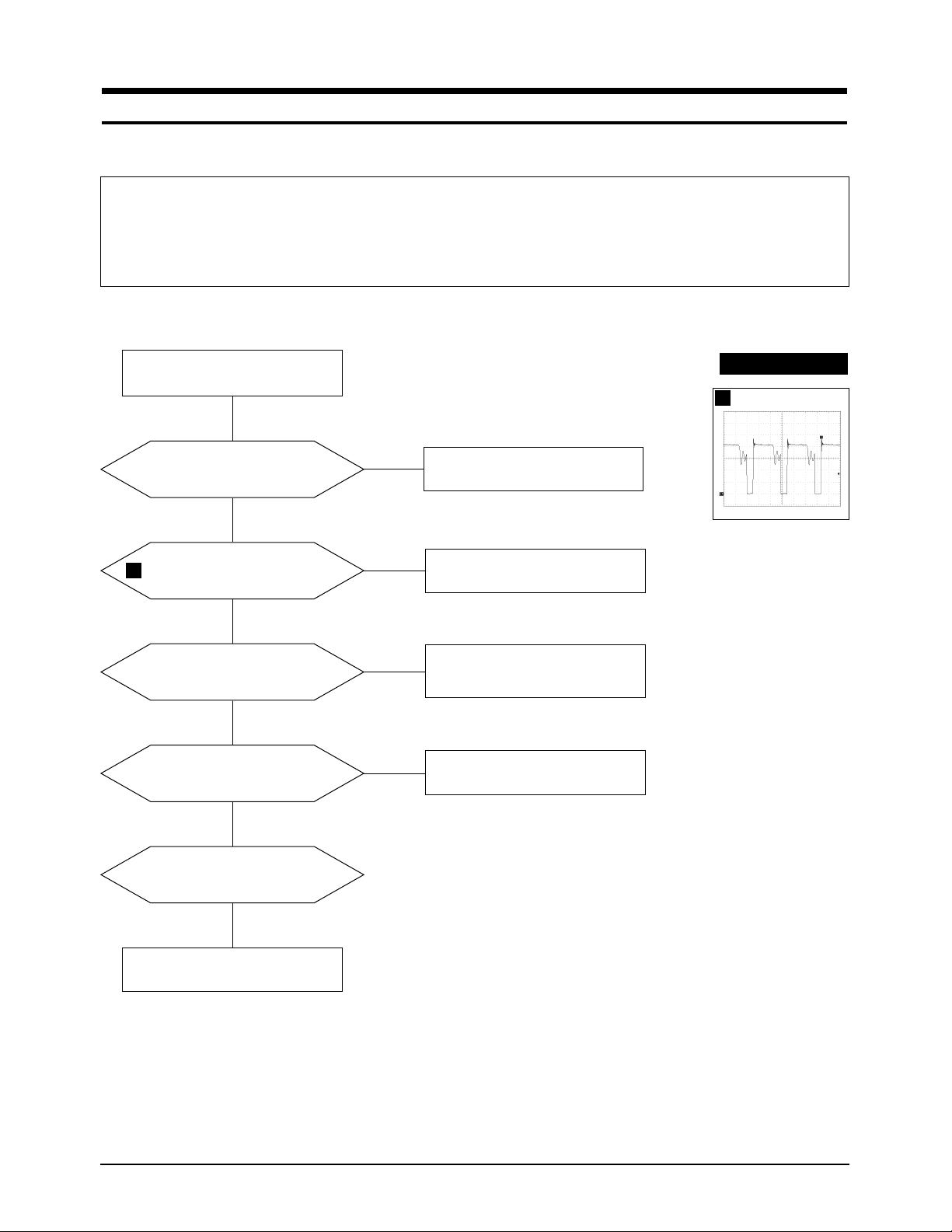
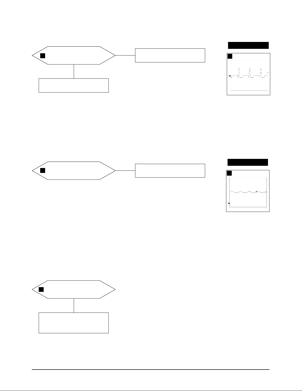
WAVEFORMS
1
1
100 V (IC601, #1)
CH1 P-P = 100 V CH1 RMS = 350.2 V
Page 2
5 Troubleshooting
5-2 PN19MT/MO/IO
x178/19P2
5-1-2 DPMS Failure
Make No H/V Sync. (power off mode)
Check signal source
H/V Sync. video level.
LED blinks?
Check IC201 Pin 39.
Yes
No
Q620 Base drive voltage?
Check IC201 Pin 10.
Check and Replace Q403.
Yes
No
Is there 12 volt?
Check IC201 Pin 9.
Check IC651.
Done
Yes
No
Page 3
5 Troubleshooting
PN19MT/MO/IO
x178/19P2
5-3
5-1-3 H_Deflection Failure
IC250 Pin 26 waveform is right?
Check IC250.
Yes
No
Q401 Gate Drain waveform
is right?
Check IC250 Pin 26.
Check Q401, R404 and 25V line.
Check Q250, Q251.
Yes
No
Check some parts around
IC261 and Q262.
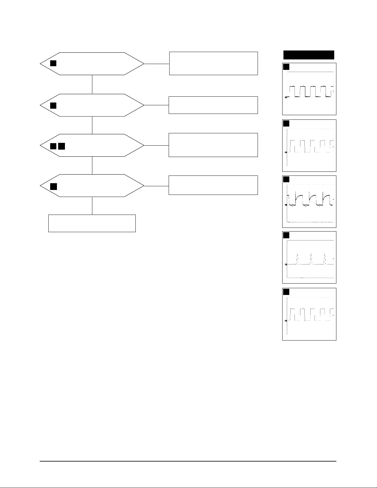
WAVEFORMS
6
3
210 V (Q454, Drain)
CH1 P-P = 210V CH1 RMS = 302V
4
66.4V (Q401, Drain)
CH1 P-P = 66.4V CH1 RMS = 25.84V
5
1.24kV (Q402, Collector)
CH1 P-P = 1.24kV CH1 RMS = 302V
Q454 Drain waveform is right?
Yes
No
Check R467, Q454, D456,
and +210V line.
Check ZD450 and IC402 Pin 6
3
4
2
Yes
Q402 Collector waveform
is right?
5
Check and replace D403 and Q402.
Check DY connector connection.
No
2
13.0 V (Q401, Gate)
CH1 P-P = 13.0V CH1 RMS = 7.91V
6
11.0V (IC250, #26)
CH1 RMS = 11.0V
Page 4
5 Troubleshooting
5-4 PN19MT/MO/IO
x178/19P2
5-1-5 H_Lin. Failure
IC201 Pin 21 voltage varies with
different H_Lin. DAC values?
IC403 Pin 7, 8 voltage varies with
different H_Lin. DAC values?
Check+12V line.
Check some parts around IC403.
Check L403.
Yes
Yes
No
Replace IC201.
No
5-1-6 Invariable H_Size
IC201 Pin 20 voltage varies with
different B_Out DAC values?
IC402 Pin6 Voltage Varies with
different H_Lin. DAC Values?
Check and replace IC402.
Yes
No
Check and replace IC201.
No
7-1-4 S Correction Failure
S1~S3 signals are right at each
frequency block?
Check S1 ~ S3 signal.
Check and replace C411~C418,
Q408~Q411, Q403~Q407.
Yes
Check and replace IC201.
No
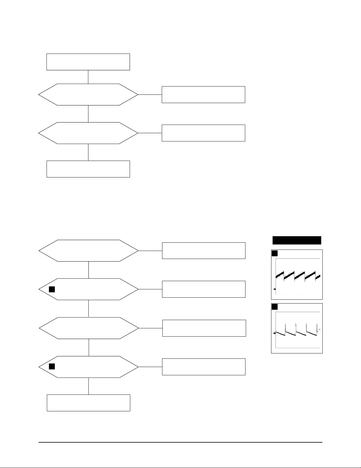
7
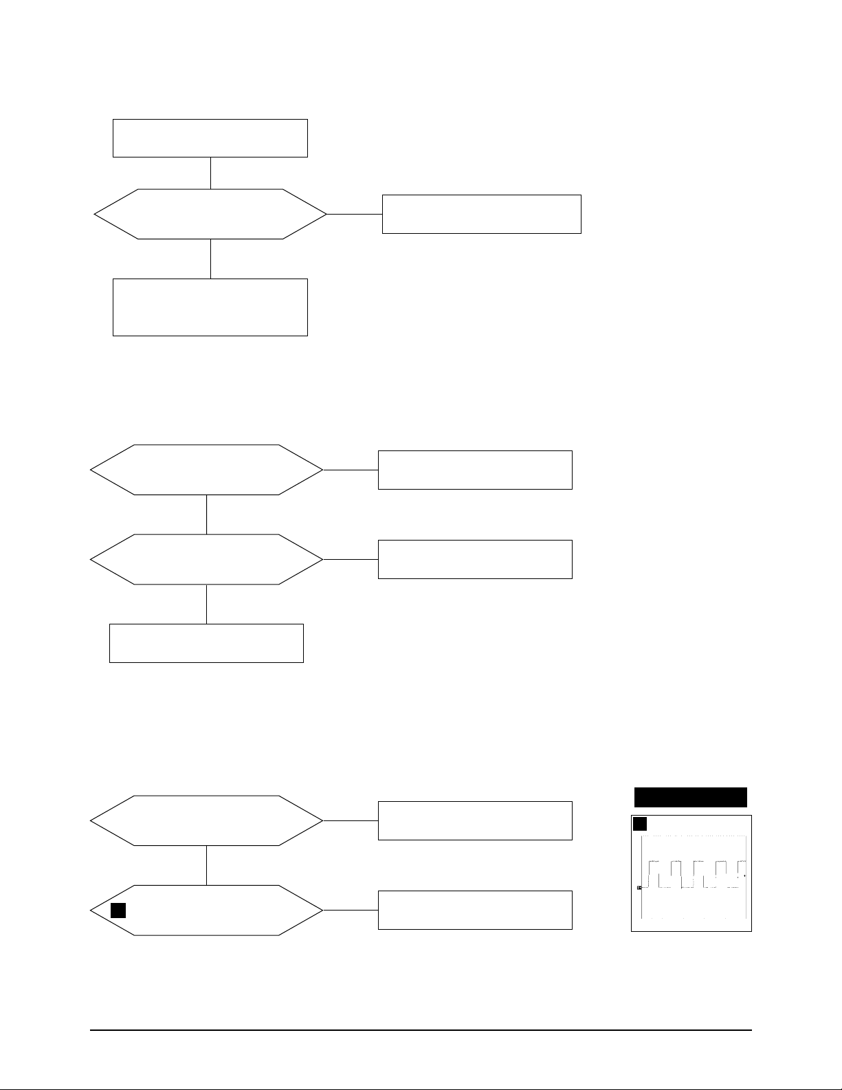
WAVEFORMS
7
13.6 V (IC402, #6)
CH1 P-P = 13.6V CH1 RMS = 9.02V
Page 5
5 Troubleshooting
PN19MT/MO/IO
x178/19P2
5-5
5-1-8 Side Pin or Trap Failure
IC250 Pin 24 output exists?
Check and replace IC250.
5-1-9 Para. or Pin Balance Failure
IC250 Pin 24 output varies with
different DAC values?
Yes
Replace IC250.
No
WAVEFORMS
9
9
IC250, #24
CH1 P-P = 1.00V CH1 RMS = 3.008 V
5-1-7 Abnormal H_Size
T402 Pin 8 waveform is right?
Check and replace T402.
Check IC402 Pin 6
and IC201 Pin 20 and 22.
Yes
No
WAVEFORMS
8
8
28.0V (T402, #8)
CH1 P-P = 28.0V CH1 RMS = 5.92V
9
Page 6
5 Troubleshooting
5-6 PN19MT/MO/IO
x178/19P2
5-1-11 V Deflection Failure
14V line is on?
IC250 Pin 23 output exists?
Check and replace IC250.
Yes
Yes
No
Refer to 5-1-1 No Power Supply
No
IC301 Pin 6 output exists?
Check and replace some parts
around R312, R316 and IC301.
Yes
No
Check V_DY connector connection.
WAVEFORMS
10
11
10
1.32 V (IC250, #23)
CH1 P-P = 1.32V CH1 RMS = 1.507 V
11
55.2 V (IC301, #6)
CH1 P-P = 55.2 V CH1 RMS = 8.04 V
5-1-10 Tilt Failure
IC201 Pin 23 output duty varies
with different DAC values?
IC403 Pin 10, 11 output varies with
different DAC values?
Check and replace IC403.
Check and replace CRT.
Yes
Yes
No
Check and replace IC201.
No
Check tilt connector connection
IC301 Pin 1 output exists?
Check and replace R301.
Yes
No
Page 7

5 Troubleshooting
PN19MT/MO/IO
x178/19P2
5-7
5-1-13 High Voltage Failure
Q504 Gate driving pulse exists?
Check +12V line.
Check and replace IC501, Q521,
Q502, Q503, and Q504.
Yes
No
Adjust the H/V Value
using the jig program.
Done
WAVEFORMS
5-1-12 V Size or Position Variation Failure
IC250 Pin 23 output varies with
different DAC values?
Yes
Check and replace IC301.
Check the Vias Voltage.
Check and replace IC250 and IC301.
No
12
10
10
1.32 V (IC250, #23)
CH1 P-P = 1.32V CH1 RMS = 1.507 V
WAVEFORMS
12
12.2 V (Q504, Gate)
CH1 P-P = 12.2V CH1 RMS = 5.30V
Page 8

5 Troubleshooting
5-8 PN19MT/MO/IO
x178/19P2
5-1-15 Dynamic Focus Failure
IC250 Pin 11, 32
output is right?
Some parts around Q551, Q552,
Q553, Q554 are right?
Replace failed part.
Yes
Yes
No
Replace the IC250.
No
Some parts around T502 is right?
Replace failed part.
Yes
No
Check the connection between FBT
Focus pin 13 and CRT Socket PCB.
WAVEFORMS
14
14
960mV (IC250, #32)
CH1 P-P = 960mV CH1 RMS = 6.043V
15
960mV (IC250, #11)
CH1 P-P = 960mV CH1 RMS = 6.043V
IC104 Pin 16 input exists and
varies with different patterns?
Check and replace IC04, Q101, Q102,
D101, +120V line.
Input full white pattern to monitor.
Yes
No
Yes
T501 Pin 8 output exists and varies
with different patterns?
Check and replace T501.
Yes
No
Done
5-1-14 ABL Failure
IC104 Pin 12 input exists and
varies with different patterns?
Check and replace IC104.
No
Check CN102.
WAVEFORMS
13
4.48 V (IC104, #16)
CH1 P-P = 4.48V CH1 RMS = 2.652V
13
15
Page 9

5 Troubleshooting
PN19MT/MO/IO
x178/19P2
5-9
5-1-16 No Video
IC104 Pin 5, 8 and 10 inputs
are right?
IC104 Pin 25, 28 and 30
outputs are right?
Check IC104 Pin 13, 14, +12V line.
Yes
Yes
No
Check and replace IC104.
No
IC105 Pin 1, 3 and 5 outputs
are right?
Check +12V line.
Check and replace IC105.
Yes
No
Cathode DC levels are right?
Check +80V line.
Check and replace IC104.
Yes
No
G2 voltage is right?
Check G2 wire, CRT Socket board
and FBT.
Change CRT.
Yes
Done.
No
Send full white pattern to the monitor
and check signal cable.
WAVEFORMS
16
17
18
16
1.08V (IC104 #5, 8, 10)
CH1 P-P = 1.00V CH1 RMS = 2.452V
17
3.52V (IC104 #25,28,30)
CH1 P-P = 3.52V CH1 RMS = 3.204V
18
46.4V (IC105, #1, 3, 5)
CH1 P-P = 46.4V CH1 RMS = 47.84V
Page 10

5 Troubleshooting
5-10 PN19MT/MO/IO
x178/19P2
5-1-17 Micom Failure
IC201 Pin 11 input is right?
IC201 Pin 13 and 14 inputs
are right?
Check C203, C204 and X201.
Yes
Yes
No
Check IC650.
No
IC201 Pin 18 input is right?
Check IC650.
Yes
No
All in/output values are right?
Replace IC201.
Yes
No
Done
WAVEFORMS
19
19
24.4V (IC201, #13, 14)
CH1 P-P = 24.4 V CH1 RMS = 6.32V
Page 11

5 Troubleshooting
PN19MT/MO/IO
x178/19P2
5-11
5-1-18 OSD Failure
IC104 Pin 17 input is right?
IC104 Pin 6 input is right?
Check and replace Q103.
Yes
Yes
No
Check and replace D302 and Q301.
No
IC104 Pin 7 and 8 inputs are right?
Check IC201 Pin 41 and 42.
Yes
No
IC104 Pin 19, 20, 21, and 22
outputs are right?
Check and replace IC104.
Check and replace IC104.
Done
No
WAVEFORMS
20
21
20
6.72 V (IC104, #17)
21
6.72 V (IC104, #6)
Check CN104 and connector Ass’y.
Yes
Yes
Page 12

5 Troubleshooting
5-12 PN19MT/MO/IO
x178/19P2
5-1-19 User Control Failure
Does the DC level change at
Pin 35, 36 of IC201 when you push
the button S/W?
Check and replace the Function Key.
No
Done
RL601 operation is right?
Q601 base input is right?
Check and replace Q601.
No
No
No
Yes
Check D-coil and TH601.
Yes
IC201 Pin 40 output is right?
Check and replace IC201.
Check the Function Key.
Yes
Yes
Done
Check degaussing connector.
5-1-20 Degaussing Failure
Check connector Ass’y.
Yes
Yes
Check and replace IC201.
R236 and R604 is right?
Check and replace R236 and R604.
No
Page 13

5 Troubleshooting
PN19MT/MO/IO
x178/19P2
5-13
5-2 General Troubleshooting
5-2-1 No Picture
LED blinks?
LED is green color?
Check the signal cable.
Check G2 voltage, high voltage
and R, G, B cathode voltage.
No
No
Yes
Refer to 5-2-2 Shut down.
Yes
5-2-2 Shut Down
Blinking LED’s?
Scan failure?
Check horizontal, vertical deflection
system and check power supply
secondary voltages.
(Refer to 5-1-3 and 5-1-11)
Yes
Yes
Check power supply.
(Refer to 5-1-1)
No
Check and replace IC201.
Done
No
Video failure?
Check Video board.
(Refer to 5-1-16)
No
Yes
High Voltage failure?
Check the high Voltage system.
(Refer to 5-1-13)
Yes
No
Page 14

5 Troubleshooting
5-14 PN19MT/MO/IO
x178/19P2
5-2-3 Missing Color
Proper Video levels are
on CN101 (D-Sub) Pin 1, 3 and 5?
Proper Video signal is
on all cathodes?
Refer to 5-1-16 No Video.
Yes
Yes
No
Check signal generator.
No
Proper DC voltage is
on all cathodes?
Check IC101 Pin 19, 20 and 21.
Check QB02, QG02, QR02, QB03,
QG03, and QR03.
Yes
Yes
No
G2 voltage is right?
Check G2 wire,
G2 Control Volume and FBT.
No
Replace CRT.
Done
WAVEFORMS
22
10.0 V (R,G,B, Video)
CH1 P-P = 10.0V CH1 RMS = 17.02V
22
Page 15

5 Troubleshooting
PN19MT/MO/IO
x178/19P2
5-15
G2 voltage is right?
Blank pulse is on IC104 Pin 17 of
video board?
Check D102 and Q103.
Check CN102 connector Ass’y..
Yes
Yes
No
Check G2 wire,
G2 Control Volume and FBT.
No
Blank padestal is on
IC104 Pin 25, 28, 30?
Check some parts around
IC104.
Done
Yes
No
Check white balance adjustment.
5-2-4 Visible Retrace
20
WAVEFORMS
20
6.72V (IC104, #17)
Page 16

5 Troubleshooting
5-16 PN19MT/MO/IO
x178/19P2
Signals are right?
Signals at Pin 3 and 4 of
CN203 are right?
Check Wire and connector.
Yes
Yes
No
Check Video Cable.
No
Signals at Pin 30 and 31 of
IC201 are right?
Check H_SYNC and V_SYNC.
Check circuits on Main board.
Yes
Done
No
Check D-Sub Connector input signals
of Pin 1, 2 and 3.
5-2-5 Unsynchronized Image
Page 17

5 Troubleshooting
PN19MT/MO/IO
x178/19P2
5-17
The convergence is now
within spec.?
Readjust convergence.
No
Done
Yes
The convergence is now
within spec.?
Done
Change CRT and readjust
convergence.
No
Done
Yes
Try readjusting convergence.
5-2-6 Misconvergence
Page 18

5 Troubleshooting
5-18 PN19MT/MO/IO
x178/19P2
Improved focus?
Check focus leads from FBT
to CRT Socket.
Check the CRT Socket.
No
Aging monitor and check for focus
change.
Yes
Dynamic focus circuit is right?
Refer to 5-1-15 Dynamic
Focus Failure.
Replace the CRT and verify focus.
Yes
No
Adjust focus VR of FBT.
5-2-7 Poor Focus
5-2-8 Purity Failure
Purity is right?
Degaussing circuit is right?
Refer to 5-1-20 Degaussing Failure.
Replace CRT and verify purity.
Yes
No
No
Done
Yes
Degaussing
 Loading...