

Page 1

PLASMA DISPLAY TV
Chassis : D72A(N)_Puccini
Model : PL50P5HX/STR
PLASMA DISPLAY TV FEATURES
■■
DTV Ready PDP TV
■
2 Way 4 Speakers
■
■
1 HDMI input
■
Slim line design
■
■
Energy Saving
■
12 Bit image processing
(687 billion color)
SERVICE
Manual
PL-50P5H
Page 2

This Service Manual is a property of Samsung Electronics Co.,Ltd.
Any unauthorized use of Manual can be punished under applicable
International and/or domestic law.
© Samsung Electronics Co., Ltd. Oct. 2005
Printed in Korea
AA82-03008A
ELECTRONICS
Page 3

Table of Contents
Chapter 1 Precaution
■ 1-1 Safety Precautions . . . . . . . . . . . . . . . . . . . . . . . . . . . . . . . . . . . . . . . . . . . . . . . . . . . . . . . . . . . 1-1
■ 1-2 Servicing Precautions . . . . . . . . . . . . . . . . . . . . . . . . . . . . . . . . . . . . . . . . . . . . . . . . . . . . . . . . 1-3
■ 1-3 Static Electricity Precautions . . . . . . . . . . . . . . . . . . . . . . . . . . . . . . . . . . . . . . . . . . . . . . . . . . . 1-4
■ 1-4 Installation Precautions . . . . . . . . . . . . . . . . . . . . . . . . . . . . . . . . . . . . . . . . . . . . . . . . . . . . . . . 1-5
Chapter 2 Product Specification
■ 2-1 Product Features . . . . . . . . . . . . . . . . . . . . . . . . . . . . . . . . . . . . . . . . . . . . . . . . . . . . . . . . . . . . 2-1
■ 2-2 Key Features . . . . . . . . . . . . . . . . . . . . . . . . . . . . . . . . . . . . . . . . . . . . . . . . . . . . . . . . . . . . . . . 2-2
■ 2-3 Specifications Analysis . . . . . . . . . . . . . . . . . . . . . . . . . . . . . . . . . . . . . . . . . . . . . . . . . . . . . . . . 2-5
■ 2-4 Accessories . . . . . . . . . . . . . . . . . . . . . . . . . . . . . . . . . . . . . . . . . . . . . . . . . . . . . . . . . . . . . . . . 2-6
Chapter 3 Alignment & Adjustment
■ 3-1 Service Instruction . . . . . . . . . . . . . . . . . . . . . . . . . . . . . . . . . . . . . . . . . . . . . . . . . . . . . . . . . . . 3-1
■ 3-2 How to Access Service Mode . . . . . . . . . . . . . . . . . . . . . . . . . . . . . . . . . . . . . . . . . . . . . . . . . . . 3-2
■ 3-3 Factory Data . . . . . . . . . . . . . . . . . . . . . . . . . . . . . . . . . . . . . . . . . . . . . . . . . . . . . . . . . . . . . . . . 3-3
■ 3-4 Service Adjustment . . . . . . . . . . . . . . . . . . . . . . . . . . . . . . . . . . . . . . . . . . . . . . . . . . . . . . . . . . 3-8
■ 3-5 Software Upgrade . . . . . . . . . . . . . . . . . . . . . . . . . . . . . . . . . . . . . . . . . . . . . . . . . . . . . . . . . . . 3-10
■ 3-6 Replacements & Calibration . . . . . . . . . . . . . . . . . . . . . . . . . . . . . . . . . . . . . . . . . . . . . . . . . . . . 3-14
Chapter 4 Exploded View & Part List
■ 4-1 PL50P5HX/STR . . . . . . . . . . . . . . . . . . . . . . . . . . . . . . . . . . . . . . . . . . . . . . . . . . . . . . . . . . . . . 4-1
Chapter 5 Electrical Part List
■ 5-1 PL50P5HX/STR Service Item . . . . . . . . . . . . . . . . . . . . . . . . . . . . . . . . . . . . . . . . . . . . . . . . . . 5-1
Chapter 6 Troubleshooting
■ 6-1 First Checklist for Troubleshooting . . . . . . . . . . . . . . . . . . . . . . . . . . . . . . . . . . . . . . . . . . . . . . . 6-1
■ 6-2 Checkpoints by Error Mode . . . . . . . . . . . . . . . . . . . . . . . . . . . . . . . . . . . . . . . . . . . . . . . . . . . . 6-2
■ 6-3 Troubleshooting Procedures by ASS'Y . . . . . . . . . . . . . . . . . . . . . . . . . . . . . . . . . . . . . . . . . . . 6-7
Chapter 7 Block Diagram
■ 7-1 Overall Block Diagram . . . . . . . . . . . . . . . . . . . . . . . . . . . . . . . . . . . . . . . . . . . . . . . . . . . . . . . . 7-1
■ 7-2 Partial Block Diagram . . . . . . . . . . . . . . . . . . . . . . . . . . . . . . . . . . . . . . . . . . . . . . . . . . . . . . . . . 7-2
Chapter 8 Wiring Diagram
■ 8-1 Overall Wiring . . . . . . . . . . . . . . . . . . . . . . . . . . . . . . . . . . . . . . . . . . . . . . . . . . . . . . . . . . . . . . . 8-1
■ 8-2 Partial Wiring . . . . . . . . . . . . . . . . . . . . . . . . . . . . . . . . . . . . . . . . . . . . . . . . . . . . . . . . . . . . . . . 8-2
Page 4

Chapter 9 PCB Diagram
■ 9-1 PDP Module, SMPS . . . . . . . . . . . . . . . . . . . . . . . . . . . . . . . . . . . . . . . . . . . . . . . . . . . . . . . . . . 9-1
■ 9-2 Video Board, Function Key Borad, Power Button Board . . . . . . . . . . . . . . . . . . . . . . . . . . . . . . 9-2
Chapter 10 Schematic Diagram
■ 10-1 Main . . . . . . . . . . . . . . . . . . . . . . . . . . . . . . . . . . . . . . . . . . . . . . . . . . . . . . . . . . . . . . . . . . . . . 10-1
■ 10-2 Function . . . . . . . . . . . . . . . . . . . . . . . . . . . . . . . . . . . . . . . . . . . . . . . . . . . . . . . . . . . . . . . . . . 10-14
■ 10-3 Power/IR . . . . . . . . . . . . . . . . . . . . . . . . . . . . . . . . . . . . . . . . . . . . . . . . . . . . . . . . . . . . . . . . . 10-15
Page 5

Operation Instruction & Installation
Samsung Electronics 11-1
11. Operation Instruction & Installation
11-1 Product Features and Functions
11-1-1 Front Panel
1
2
3
4
5
1 SOURCE button
Press to display all of the available video
sources (TV, AV, S-Video, Component1,
Component2, PC, and HDMI).
2 MENU button
Displays the main on-screen menu.
3 VOL +, -buttons
Press to increase or decrease the volume.
Also used to select or adjust items on the
on-screen menu.
4 CH( , ) buttons
Press CH or CH to change channels.
Also used to move up or down in the on-screen
menu.
678
5 (Enter) button
Press to confirm a selection.
6 Power button
Press to turn the TV on and off.
Power indicator
- Power Off : Blue
- Power On : Off
7 Remote Control Sensor
Aim the remote control towards this spot on
the TV.
8
Speakers
Page 6

Operation Instruction & Installation
11-2 Samsung Electronics
11-1-2 Rear Panel
1 POWER IN
Connect the supplied power cord.
2 SERVICE ONLY
Connector for service only.
3 HDMI/DVI IN
Connect to the HDMI jack of a device with
HDMI output.
These inputs can also be used as a DVI
connection with separate analog audio inputs.
An optional HDMI/DVI cable will be
necessary to make this connection.
When using the optional HDMI/DVI adapter,
the DVI analog audio inputs on your TV allow
you to receive left and right audio from your
DVI device. (Not compatible with PC)
4 DVI AUDIO IN (AUDIO-L/R)
Connect to the DVI audio output jack of an
external device.
5PC IN
Connect to the video output jack on your PC.
6 PC AUDIO IN
Connect to the audio output jack on your PC.
7 COMPONENT IN 1, 2
Video (Y/PB /PR) and audio (L-AUDIO-R)
component inputs.
8 ANT IN
75 Ω Coaxial connector for Antenna/Cable
Network.
9 AV OUT (VIDEO / AUDIO L/R)
Outputs for external devices.
10 AV IN (VIDEO / AUDIO L/R)
Video and audio inputs for external devices,
such as a camcorder or VCR.
11 S-VIDEO
Video input for external devices with an
S-Video output, such as a camcorder or VCR.
Page 7

Operation Instruction & Installation
Samsung Electronics 11-3
11-1-3 Remote Control
Page 8
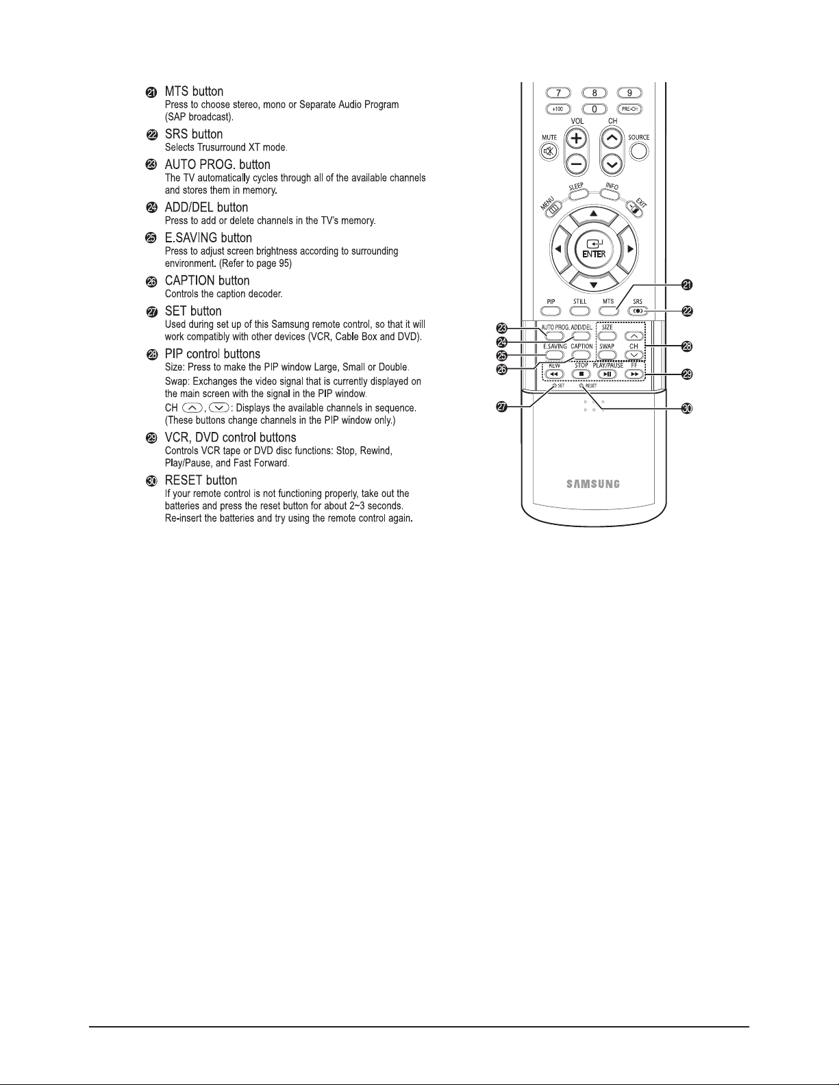
Operation Instruction & Installation
11-4 Samsung Electronics
Page 9

Operation Instruction & Installation
Samsung Electronics 11-5
11-2 New Features
11-2-1 Power Saving Mode (Applies to the "Settings" of the User Menu)
1. Objectives
- To enhance a sensible visual quality by maintaining an appropriate screen brightness according to the ambient brightness and
to reduce power consumption.
- To improve the power consumption efficiency when Power Saving Mode is selected.
2. Details
The CPU PW318 of the Video Board takes the current ambient brightness (in Lux units) stored in the Ambient Light Sensor of the
Power Assy., which is attached at the front of the PDP, at given intervals through SMBUS communication (identical to I2C) and
controls the PDP module to operate with the appropriate illuminance. The I2C bus is used to communicate with the PDPmodule,
and the communication method is the same as the existing communication method.
- Location of the Ambient Light Sensor
The sensor is attached to the Power Assy., which is on the front of the PDP. The location of the sensor on the Power Assy. is
displayed in the figure below. External light reaches the sensor through the guide of the Power Assy.
The screen brightness is adjusted according to the brightness measured by the Ambient Light Sensor, using the Multi APC
function (controls the number of sustain pulses according to the average signal levels) of the PDP panel, thus reducing power
consumption.
The Ambient Light Sensor IC
detects the amount of illumination.
Page 10

Operation Instruction & Installation
11-6 Samsung Electronics
11-2-2 PIP Settings (X - PIPdoesn't operate, O - PIPand swap operate)
Main screen
PIP screen
TV AV S-Video Component 1 Component 2 PC HDMI
TV X
○ ○ ○ ○ ○ ○
AV
○
X
○ ○ ○ ○ ○
S-Video
○ ○
X
○ ○ ○ ○
Component 1 X X X X X X X
Component 2 X X X X X X X
PC X X X X X X X
HDMI X X X X X X X
Note : This TV has only one tuner and does not allow you to watch one TV channel in the main screen and another channel in the
PIP screen.
Press the MENU button. Press the or button to select
“Picture”, then press the ENTER button.
1
Quick way to select Energy Saving: Simply press the “E.SAVING”
button on the remote control.
Press the or button to select “Energy Saving”, then
press the ENTER button.
2
Press the or button to select submenu (Auto Saving,
Standard, or Super Saving) you want, then press the
3
ENTER button.
• Auto Saving : Automatically adjusts to the
surrounding illumination.
• Standard : Operates in standard mode
regardless of the surrounding
illumination.
• Super Saving : Enters maximum power saving
mode regardless of the surrounding
illumination.
TV
Mode : Dynamic
Size : Wide
Digital NR : On
DNIe Demo : Off
My Color Control
Energy Saving : Standard
PIP
TV
Mode : Dynamic
Size : Wide
Digital NR : On
DNIe Demo : Off
My Color Control
Energy Saving : Sta
PIP
TV
Mode : Dynamic
Size : Wide
Digital NR : On
DNIe Demo : Off
My Color Control
Energy Saving : Stan
PIP
Picture
√
√
√
√
√
√
√
Move Enter Return
Picture
Auto Saving
Standard
Super Saving
Move Enter Return
Picture
Auto Saving
Standard
Super Saving
Move Enter Return
Press the EXIT button to exit.
4
Page 11

Operation Instruction & Installation
Samsung Electronics 11-7
11-3 Installation Notes and Precautions
11-3-1 Installation Notes
1. Contact a technician for installing the wall bracket.
2. Samsung Electronics is not responsible for any damage to the product or injury to yourself or others if you elect to perform the
wall installation.
3. This product is for installing on cement walls. The product may not stay in place when installed on plaster or wood.
11-3-2 Parts (Wall attachment panel is sold separately)
Only use the components and accessories shipped with the panel.
Wall Bracket Hinge Accessories
Plastic Hanger : 4
Screw : 4
Screw : 11
Anchor : 111 Left : 1 Right : 1
Page 12

Operation Instruction & Installation
11-8 Samsung Electronics
11-3-3 How to assemble the Wall Mount Bracket
Insert and tighten the Captive Screw in the direction of the arrow.
When done, mount the wall bracket on the wall.
1
Captive Screws
Hinge (Left)
Wall Bracket
Before drilling into the wall, check if the
length between the two locking holes at
2
the back of the product is correct.
If the length is too short or long, loosen
all or some of the 4 screws on the wall
bracket to adjust the length.
Length between the
two locking holes
There are two hinges
(left and right). Use the
correct one.
Hinge (Right)
Check the installation diagram and mark
the drill points on the wall.
3
Use the 5.0 mm bit to drill holes deeper
than 35 mm. Fix each anchor in the
corresponding hole.
Match each of the brackets and hinge
holes to the corresponding anchor holes
and insert and tighten the 11 screws .
Page 13

Operation Instruction & Installation
Samsung Electronics 11-9
11-3-4 Fixing the TV panel to the wall attachment panel bracket
Remove the 4 screws on the back of the product.
1
Insert the screw into the plastic hanger. (See the figure below)
2
• Mount the product on the wall bracket and make sure it is properly fixed to the left and
right plastic hangers.
• Be careful when installing the product on the bracket as fingers can be caught in the holes.
• Make sure the wall bracket is securely fixed to the wall, or the product may not stay in
place after installation.
Tighten the 4 screws in step 2 (plastic
hanger + screw ) to the rear holes of
3
the product.
Remove safety pin ( ) and insert the 4
product holders into the corresponding
4
bracket holes ( ). Then place the
product ( ) so that it is firmly fixed to
the bracket. Make sure to reinsert and
tighten the safety pin ( ) to securely
hold the product to the bracket.
PDP
Wall Bracket Wall
Page 14

Operation Instruction & Installation
11-10 Samsung Electronics
11-3-5 How to Adjust Mounting Angle
Note : Adjust the bracket angle to -2
Note
o
before installing it on the wall.
Change Angle
Fix the product to the wall bracket.
1
Hold the product at the top in the center and
pull it forward (direction of the arrow) to
2
adjust the angle. (See the figure to the right)
You can adjust the bracket angle between -2°
and 15°.
3
How to Adjust Mounting Angle
Make sure to use the top center, and not the
left or the right side of the product to adjust
the angle.
Notes
• Contact an authorized technician when installing the wall attachment panel.
• After hanging the TV panel on the wall attachment panel, make sure that the Insulation holders are
completely secured.
• Be careful not to get your fingers caught during installation.
• Make sure the wall attachment panel brackets are tightened. Otherwise, the TV panel may
fall down.
• Please secure the mounting bracket on the wall surface after setting its angle at 0°.
Page 15

Operation Instruction & Installation
Samsung Electronics 11-11
11-3-6 How to assemble the Stand-Base
Using the 4 screws for securing the stand pegs and the monitor, firmly attach the monitor
to the stand pegs. (The exterior of the set may be different than the picture.)
1
Warning
Firmly secure the stand to
the TV before moving it, as
the stand may fall and
could cause serious injury.
Two or more people should carry the TV. Never lay the TV on the floor because of possible damage to the screen.
Always store the TV upright.
Page 16

11-12 Samsung Electronics
MEMO
Page 17

Part Name Description Description Photo
Cover-
Stand
① Remove 4 screws on the SPEAKER-COVER
: BH,+,B,M4,L12,ZPC(BLK)
② Remove the SPEAKER-COVER.
Disassembly & Reassembly
Samsung Electronics 12-1
12. Disassembly & Reassembly
12-1 Overall Disassembly & Reassembly
12-1-1 Separation of Stand
Part Name Description Description Photo
Stand
① Remove 4 screws.
: PH,+,WSP,S,M4,L35,ZPC(BLK)
② Pull the stand down to remove it from the unit.
: Please lay the PDP unit face down on a soft surface when
removing the stand.
12-1-2 Separation of ASSY COVER-STAND CABLE
Notice
- Be sure to separate the power cord before disassembling the unit.
- Discharge the capacitors first when separating PCB's with high capacity capacitors such as SMPS, X Drive Board, Y Drive
Board, etc. (Aspark may be generated by the electric charge, and there is danger of electronic shock.)
- Check that the cables are properly connected referring to the circuit diagram when disassembling or assembling the unit taking
care not to damage the cables.
- Take care not to cause a flaw in the Glass Filter in the front.
- Assemble the boards in the reverse order of the disassembly.
- The plasma must be layed down on a flat padded surface for disassembly and reassembly.
Page 18

Disassembly & Reassembly
12-2 Samsung Electronics
12-1-3 Separation of ASSY COVER P-REAR TOP
Part Name Description Description Photo
Rear
Top
① Remove the 9 screws on the cover rear.
: BH,+,-,S,M4,L8,ZPC(BLK)
② Remove the 2 Hex nuts for the PC input.
: M3,L6,NI PLT,SUM24L,#4-40
③ Remove the cover rear.
12-1-4 Separation of ASSY POWER & IR Board
Part Name Description Description Photo
Power &
IR Board
① Remove 2 screws on the POWER IR Assy
: BH,+,B,M4,L12,ZPC(BLK)
② Remove the ASSY POWER IR Board.
12-1-5 Separation of ASSY COVER SPEAKER
Part Name Description Description Photo
Cover
Speaker
① Remove the 14 screws on the speaker cover.
: BH,+,B,M4,L12,ZPC(BLK)
② Remove the SPEAKER-COVER.
Page 19

Disassembly & Reassembly
Samsung Electronics 12-3
12-1-6 Separation of ASSY COVER P-REAR
Part Name Description Description Photo
Rear
① Remove 23 screws.
: BH,+,-,S,M4,L8,ZPC(BLK)
② Remove 4 screws.
: M8,L16,ZPC(BLK)
③ Remove the Back Cover.
12-1-7 Separation of ASSY PCB MISC-MAIN
Part Name Description Description Photo
Main
Board
① Remove 4 screws
: PH,+,WWP,M3,L8,NI PLT
② Remove all connectors from the board.
③ Remove the Main Board.
12-1-8 Separation of ASSY COVER P-REAR SUB
Part Name Description Description Photo
Cover P-
Rear Sub
① Remove 4 screws.
: BH,+,-,S,M4,L8,ZPC(BLK)
② Remove 2 screws.
: BH,+,B,M4,L8,ZPC(BLK)
③ Remove the sub cover.
Page 20

Disassembly & Reassembly
12-4 Samsung Electronics
12-1-10 Separation of ASSY LOGIC BOARD
Part Name Description Description Photo
Flat Cable
① Take care when separating the Logic Board not to damage
the Flat-Cable Connector Cover.
Logic Board
① Remove 4 screws.
: PH,+,WWP,M3,L8,NI PLT
② Remove the Logic Board.
Part Name Description Description Photo
SMPS
SMPS DC-
DC
① Remove 8 screws.
: PH,+,WWP,M3,L8,NI PLT
② Detach all connectors from the ASSY SMPS then remove the
boards.
③ Remove 4 screws.
: PH,+,WWP,M3,L8,NI PLT
④ Detach all connectors from the ASSY SMPS DC DC then
remove the board.
: Wear gloves when handling the power board as there may
be some remaining electrical charge in the capacitor.
Specifically, avoid touching any part of the capacitor.
12-1-9 Separation of ASSY SMPS and ASSY SMPS DC-DC
Page 21

Disassembly & Reassembly
Samsung Electronics 12-5
12-1-11 Separation of ASSY X DRIVE BOARD
Part Name Description Description Photo
X-Drive
Board
① To separate the Flat Cable of the X-Board, press the upper
and the lower sides of the connector.
① While pressing the connector, apply slight force toward the
direction of the cable to release the connector.
① Remove the Flat cable.
① Remove 6 screws.
: PH,+,WWP,M3,L8,NI PLT
② Detach all reamining connectors from the X-Drive Board.
③ Remove the X-Drive Board.
Page 22

Disassembly & Reassembly
12-6 Samsung Electronics
12-1-12 Separation of ASSY Y DRIVE BOARD
Part Name Description Description Photo
Flat Cable
① Detech the 6 Scan Board connectors from the Panel Assy by
pulling the holder from both the top and bottom ends.
Y-Scan
① Remove 5 screws.
: PH,+,WWP,M3,L8,NI PLT
Connectors
① Separate the Scan Boards from the Y-Main Board by
detaching the 2 connectors and remove the Scan Boards.
Y Drive
① Remove 8 screws.
: PH,+,WWP,M3,L8,NI PLT
② Detach all connectors from the Y-Main Board and remove the
Y-Main Board.
Page 23

Disassembly & Reassembly
Samsung Electronics 12-7
12-1-13 Separation of ASSY BUFFER BOARD
Part Name Description Description Photo
Wall
Bracket
① Remove 8 screws.
: BH,+,-,S,M4,L8,ZPC(BLK)
② Separate PDPmodule from Front cover.
: Please lay the PDP panel face down on a soft surface when
separating front cover.
③ Remove 16 screws.
: BH,+,S,M4,L10,ZPC(BLK)
TCP Cover
① Remove 8 screws.
: PH,+,WWP,M3,L8,NI PLT
② Remove TCPcovers.
Buffer
(TOP)
① Remove 12 screws.
: PH,+,WWP,M3,L8,NI PLT
② Remove the E-Board, F-Board and G-Board.
Buffer
(BOT)
① Remove 12 screws.
: PH,+,WWP,M3,L8,NI PLT
② Remove the E-Board, F-Board and G-Board.
Page 24

12-8 Samsung Electronics
MEMO
Page 25

Circuit Description
Samsung Electronics 13-1
13. Circuit Description
13-1 Power ON/OFF Signal Timing Sequence
µ
1. When connecting the AC power cord, Stand-By 5V from the Main SMPS is supplied to the Main Board (Pin 3 of CN1002 of Main
Board).
2. When pressing the Power button on the remote control or on the main body, PS_ON (Pin 5 of CN1002 of Main Board)
changes from High to Low.
3. If the PS_ON signal changes to Low, the Main SMPS supplies power to the Main Board and Logic Board, and Va and Vg power
is supplied to the DC-DC SMPS.
4. If the VS_ON signal from the Logic Board changes from Low to High, the Main SMPS supplies VS power to the X and Y Drive
Board through the DC-DC SMPS, and the screen displays a picture on it.
FFO/NO REWOP CA
,yBdnatS
)stuptuo noitpO POP(
)woL evitcA( NOSP
lanretxE SP morf
)FFO/NO rellortnoc etomeR(
tuptuo CFP
NO rellortnoC etomeR
O ot t
.ceS m 07
S m 07
ffo-nrut pets ybdnatS
NO REWOP CA
NO P A
FFO
F
NO ellortnoC etomeR
ot t
rofµ
V 5
V 5
V 4.3
V 4.3
teser rossecorp-
aV
STUPTUO CD
STUPTUO CD
tV,pmaV,V21,V5.6A,V3.5D
STUPTUO
gV
)hgih evitcA( NOSV
lanretxE S/P morf
TUPTUO CD
sV
FFO / NO YALPSID
acV
NOSV
NOSV
scV
NO YALPSID
D
NOSV
NOSV
NO YALPSID
PI
Page 26

Circuit Description
13-2 Samsung Electronics
13-2 Partial Block Description
13-2-1 Main Board
No Name Function Description
①
SVP-EX62 Main Video Decorder+Deinterlacer+Scaler
AScaler IC that generates the output resolution appropriate to the PDP panel and
generates the PIP screen.
②
DNIe-L Image Enhancer The DNIe IC for visual quality improvement.
③
M30620SPGP Main Micom Generates various control signals required for operating the circuit.
④
SAA7119 Sub Video Decorder
The Video Decoder IC that converts the Y/C and Scart RGB signals for the main
screen into 10 bit digita R, G, B signals.
⑤
SIL9993 HDMI Decorder Converts the TMDS signal on the HDMI input into 8 bit digital R, G, B signals
⑥
S3F8668 Sub Micom
Detects the Power on/off signal from the remote control and the Power button and
turns SMPS on or off, handles the Caption signal, and controls the signal for the
LEDs on the front panel.
⑦
MSP4410G Sound processor Sound Processing IC
⑧
NSP6241 Sound Effect chip Sound PWM IC
⑨
TMQZ6-405A Tuner Tuner CH Tuning and CVBS, SIF
Page 27

Circuit Description
Samsung Electronics 13-3
13-2-2 Power Button Board
13-2-3 Function Key Board
Function Key. Located on the side of the unit.
No Loc. No. Description
(1) RM01 Remote Control Sensor
(2) SW001 Power Button
(3) OP001
The Illumination sensor that senses the quantity of
light. It senses the illumination and automatically
adjusts the screen brightness according to the
surrounding brightness when the Power Saving
Mode of the User menu is set to Auto.
Page 28

Circuit Description
13-4 Samsung Electronics
(1) CN800: AC IN (90 ~ 264V)
※ CN811, CN806, CN807 and CN808 are not used.
13-2-4 Main SMPS
(2)
CN804-2
(MAIN SMPS)
↔
CN109(READY B'D)
Pin No Signal
1 ■
FAN-D
2 FAN-ON
3 STB5V
4 RTN
5 PS-ON
6 12V
7 RTN
8 RTN
9 VCA
10 VCS
11 RTN
12 5.3V
13 RTN
14 5.3V
(3)
CN803(MAIN SMPS)
↔
CN108(READY B'D)
Pin No Signal
1 ■
RTN
2 VT(33V)
3 RTN_AMP
4 RTN_AMP
5 18V_AMP
6 18V_AMP
7 RTN
8 12V
9 RTN
10 6V
(4)
CN810(Main SMPS)
↔
CN2013(Logic B'D)
Pin No Signal
1 ■
5.3V
2 5.3V
3 RTN
4 RTN
5 5.3V
6 RTN
7 PS-ON
8 N.C
9 VS-ON
10 STB 5V
(5)
CN809(Main SMPS)
↔
CN3(DC-DC SMPS)
Pin No Signal
1 ■
5.3V
2 Vg
3 RTN
4 RTN
5 RTN
6 RTN
7 RTN
8 Va
9 Va
10 N.C
11 Vs
12 Vs
Page 29

Circuit Description
Samsung Electronics 13-5
1. Outline (PDP 42inch/50inch SMPS)
Considering various related conditions, the switching regulator with good efficiency and allowing for its small size and light weight
was used as the power supply for PDP 42inch(Schubert)/50inch(Strauss), VS requiring high power consumption Asymmetrical Half
Bridge converter and flyback converter. To comply with the international harmonics standards and improve the power factor, active
PFC(Power Factor Correction) was used to rectify AC input into +400V DC output, which in turns used as input to the switching
regulator.
2. Input
The power supply shall be capable of supplying full rated output power over free voltage ranges that are rated 100 VAC - 240 VAC
RMS nominal. Operating voltage : 90 VAC - 264 VAC
The power supply must be able to start up under peak loading at 90V AC. The power supply shall automatically recover from AC
power loss. (Note that nominal voltages for test purposes are considered to be within +/- 1.0V of nominal).
STD_5V & Vpr2(3.3V) is a SELV standby voltage that is always present when AC mains voltage present.
3. Output
4. Over Voltage Protection
The over voltage sense circuitry and reference shall reside in package that are separate and distinct from the regulator control
circuitry and reference. No single point fault shall be able to cause a sustained over voltage condition on any or all outputs.
The supply shall provide latch-mode Over Voltage Protection as defined below.
5. Short Circuit and Over current Protection
An output short circuit is defined as output impedance of less than 300mohms. The power supply shall shutdown and latch off for
shorting VS DC rails to return. Shorts between main output rails and STD_5V shall not cause any damages to the power supply.
The power supply shall either shutdown and latch off until the short condition is removed, at which point the P/S shall recover.
The power supply shall be capable of withstanding a continuous short-circuit to the output without damage or over stress to the
unit (components, PCB traces,connectors,etc.) under the input conditions specified in Section 3 above. Current Protection as
defined below.
Output Name Output Voltage Output Current(Max.) Using in PDPDriving
VS +190V ~ 220V (210V) 2.0A Sustain Voltage of Drive Board
VA +60V ~ 80V (70V) 3.0A Address Voltage of Drive Board
D5.3V +5.3V 5.0A
A6.5V +6.5V 3.0A
FAN_9V +9V 0.2A
VG +15V 1.0A
D12V +12V 1.5A
A12V +5.3V 0.5A
18VAMP +18V 2.5A Amp Voltage of Audio Board
VT +33V 0.006A
STD_5V +5V 1.0A Standby for Remote Control
Parameter Min Unit
VS(210V) 250 ~ V
VA(70V) 100 ~ V
VCC(+5.3V) 6.8 ~ V
Output Over Current Limit Unit
VS(210V) 20A, Constant Current.(TBD) A
VA(70V) 10A, Constant Current.(TBD) A
Output except Vs,Va No damage (Auto Recovery or Shut down.) A
Page 30

Circuit Description
13-6 Samsung Electronics
(6) D5.3V, Vg, Ve Test Point
(7) Va, Vset, Vscan Test Point
13-2-5 DC-DC SMPS
(1)
CN809(Main SMPS)
↔
CN3(DC-DC SMPS)
Pin No Signal
1 ■
5.3V
2 Vg
3 RTN
4 RTN
5 RTN
6 RTN
7 RTN
8 Va
9 Va
10 N.C
11 Vs
12 Vs
(4), (5)
CN1, CN6
(DC-DC SMPS)
↔
CN2501(E-Buffer),
CN2701(G-Buffer)
Pin No Signal
1 ■
RTN
2 N.C
3 5.3V
4 N.C
5 Va
(2)
CN2(DC-DC SMPS)
↔ CN5007(YB'D)
Pin No Signal
1 ■
Vs
2 Vs
3 RTN
4 RTN
5 Vset
6 RTN
7 Vscan
8 RTN
9 Vg
10 5.3V
(3)
CN4(DC-DC SMPS)
↔ CN4000(X B'D)
Pin No Signal
1 ■
Vs
2 Vs
3 RTN
4 RTN
5 Ve
6 RTN
7 RTN
8 Vg
9 5.3V
Page 31

Circuit Description
Samsung Electronics 13-7
DC DC SMPS receives Vs input (195~215V) from the Main SMPS and the necessary Vscan, Vset and Ve voltages are output to
operate the PDP Module as shown in the block diagram above.
1. Block Diagram
Vs Input Part Vscan Output
Transformer
Control
and
Switching Block
Control
and
Switching Block
Control
and
Switching Block
Auxiliary
Power
Transformer
Auxiliary
Power
Transformer
Auxiliary
Power
Rectification
Block
Feedback
Block
Rectification
Block
Feedback
Block
Rectification
Block
Feedback
Block
Vset Output
Ve Output
Page 32

Circuit Description
13-8 Samsung Electronics
13-2-6 PDP Module
No Assy Name Description
①
ASSY PDP P-X MAIN BOARD X Drive Board
②
ASSY PDP P-Y MAIN BOARD Y Drive Board
③
ASSY PDP P-Y BUFF UPPER BOARD Y Buffer Upper Board
④
ASSY PDP P-Y BUFF LOWER BOARD YBuffer Lower Board
⑤
ASSY PDP P-LOGIC BOARD Logic Board
⑥
ASSY PDP P-ADDRESS E BUFF BOARD Address E Buffer Board
⑦
ASSY PDP P-ADDRESS F BUFF BOARD Address f Buffer Board
1. Logic Block
■ Logic Block Diagram
Page 33

Circuit Description
Samsung Electronics 13-9
■ A name of main part of Logic Board and vocabulary.
Item Name Explanation
①
LVDS Connector
The connector to receive the RGB, H, V, DATAEN and DCLK signals that have been LVDS encoded through the
video board. At present, there are 2 LVDS, both internal and external, and only LVDS will be provided in the final
version of the board.
②
Operating Status LED
The LED that shows whether the Sync and Clock signal is properly supplied to the logic board (Normal Status:
Blinks at 0.8 second intervals)
③
I2C Connector The connector for the Key Scan board that checks and controls the 512K data.
④
MICOM(ARM-PROCESSOR)
512K including the Gamma Table, APC Table, drive waveform timing and other options is saved to internal flash
memory.
⑤
Y Connector The connector to output the control signal for the Y drive board.
⑥
X Connector The connector to output the control signal for the X drive board.
⑦
CN2075(E-Adderss Buffer Connector) The connector to output the address data and the control signal to the E-buffer board.
⑧
CN2076(F-Adderss Buffer Connector) The connector to output the address data and the control signal to the F-buffer board.
⑨
Power Connector The connector to receive power (5V, 3.3V) for the Logic board.
⑩
ASIC CHIP The main processor that generates and outputs the logic drive signal and the address data.
⑪
MICOM LOADING 5PIN CONNECTOR The connector to load the Micom drive program. The program is loaded by connecting to the GA-WRITER.
⑫
VTOGG TPfor V Sync Check
■ About Logic Board
The Logic Board consists of a Logic Main board, which processes the video signal input through LVDS and creates the address
driver output and XY drive signals, and a Buffer board, which buffers the output signal and outputs the signal to the Address Driver
IC (TCP IC).
Logic Board Function Remark
Logic Main
- Video Signal Processing (W/L, error diffusion, APC)
- Outputs the Address Driver Control and Data Signals to the Buffer board.
- Outputs the XY Drive Board Control Signal
Buffer Board
E Buffer Board Outputs data and control signals to the bottom left TCP IC.
F Buffer Board Outputs data and control signals to the bottom right TCP IC.
1
5
01
9
3
11
4
7
2
21
6
8
Page 34

Circuit Description
13-10 Samsung Electronics
■ Major Check Points and Waveforms
- The waveform during a Normal Operation
When the PDP set and the Logic Board are properly operating, the Operation Status LED blinks at approximately 0.8 second
interval as shown in Figure 1.
If the set is out of order, check the Operation Status LED first, and check that the output waveform is normal using an
oscilloscope.
Check if the waveform is the same as shown in Figure 2 by connecting the oscilloscope to the No. 12 TP in Figure 1. Check if
the waveform is the same as in Figure 3 by connecting the oscilloscope to the connector that is connected to the Buffer board.
If the measured waveform is different from the following waveforms, the board must be replaced.
To check the waveforms, refer to the following waveform patterns.
Figure 2. Normal V-SYNC Output Waveform Figure 3. Normal Address Data Output Waveform
Page 35

Circuit Description
Samsung Electronics 13-11
1. X, Y Control Block
■ Drive Circuit Definition
The Drive Circuit is a circuit that generates a waveform (high-voltage pulse) for the X and Y electrode group of the panel's external
port so as to control the panel. The high-voltage switching pulse is generated through the combination of the IC HYBRID (Drive
block + IGBT) and FET.
■ Drive Circuit Mechanism
Apicture is displayed on the PDPby applying voltage to the X, Y and ADDRESS electrodes of each pixel according to the appropriate condition. The drive waveform applied to 42HD V4 is of the ISSS (ISSS: Interweaving Scan and Selective Sustain with Scan
IC) type and has IDS (InDependent Sustain) in the Scan section unlike the existing ADS. Discharges within a PDPpixel can be
classified into 3 types:
① Address Discharge: To form a wall voltage within the pixel by giving information (applying DATA voltage) to the pixel to be lit.
② Sustain Discharge: Sustain Discharge is a display section that voluntarily maintains the discharge of the pixels whose wall
voltage has been formed by the Address Discharge. (Optical output for displaying a picture is generated).
③ Erase Discharge: To selectively perform Address Discharge for each pixel, all pixels on the panel should be in the same status
(the wall electric charge status and space electric charge status must be the same). Therefore, the Erase
Discharge section is an important component for guaranteeing the drive margin, and is implemented by
various methods such as applying a log waveform. However, the current 42HD V4 has adopted a wall voltage
control through an RA(Repeated Auto-quenching) reset that separates the discharge area and performs
switching to perform an efficient erase operation, while the gradient was the same in the RAMP section in the
existing approach.
1) Address Discharge
Adischarge that is caused by the difference between the plus electric potential (Va apply voltage of 65~70V + Positive Wall
Charge) of the electrode and the negative electric potential (Applied GND Level + Negative Wall Charge) of the Yelectrode. The
Address discharge forms a wall voltage within the pixel to display color (to be discharged) before the Sustain Discharge period.
That is, the pixel whose wall charge has been formed by the Address Discharge forms a Sustain Discharge vis the following
Sustain pulse.
2) Sustain Discharge
ASustain Discharge is a Self-Sustaining Discharge formed by the accumulation of the electric potential of the Sustain pulse (generally 200 ~ 210 Volt) alternating over the X and Yelectrodes during the sustain period, and the wall charge depending on whether
the pixel has previously been discharged or not. That is, it is controlled by the memory characteristics, one of the basic characteristics of the AC PDP(in that the past operating conditions determine the current status). That is, if a wall voltage exists on the pixel
(if the pixel is on), a discharge is formed again because the applied voltage, which is the sum of the following applied Sustain voltage and the wall voltage, is higher than the discharge threshold voltage. If no wall voltage exists on the pixel (if the pixel is off), a
discharge will not occur because the Sustain voltage is not higher than the discharge threshold voltage. The Sustain Discharge
period is the period for generating actual optical output so as to display a picture on the PDP screen.
3) Erase Discharge
The purpose of a Reset (Erase) Discharge is to create uniformity of the wall voltage within all panel pixels. It evens the wall voltages regardless of the Sustain Discharge in the previous stage. The Erase Discharge has to remove the wall voltage introduced by
the Sustain Discharge by supplying ions or electrons by a discharge. When the wall voltage is removed through a discharge, the
time when the reverse polarity is applied to the wall voltage (fine width erasing) is to be limited or ions or electrons are to be supplied by a weak discharge (low voltage erasing) so as to prevent a wall charge in reverse polarity.
There are 2 known weak discharge (low-voltage) erase methods. 1) Alog waveform adopted by F company and 2) a weak erase
discharge via a ramp waveform adopted by Matsushita and other companies. Both methods control the externally applied voltage
by the difference of the wall voltage of the pixel by applying the rising gradient of the erasing waveform slowly, because the discharge begins when the sum of the existing remaining wall voltage and the rising waveform voltage exceeds the drive threshold
voltage. In addition, a weak discharge is introduced, because the applied voltage is low.
Page 36

Circuit Description
13-12 Samsung Electronics
■ Drive Circuit Operating Block Diagram
- Y Drive Board
- X Drive Board
■ Requisite Components Necessary for Drive Board Operation
- Power : Supplied from the power board. The optimal value may differ from the following:
a) Vs : 205V - Sustain
b) Vset : 195V - Y Rising Ramp
c) Ve : 100V - Ve bias
d) Vscan : -190V - Scan low bias
e) Vnf : -175V - Y falling Ramp (Created by the DC-DC power block of the YDrive board)
f) Vsc_h : -70V - Scan high bias (Created by the DC-DC power block of the Y Drive board)
g) Vdd : 5V - Logic signal buffer IC and IPM
h) Vcc : 15V - Gate drive IC ¹× IPM
- Logic Signal : Supplied by the Logic board. Gate signal of each switch
Logic Signal Input Part
Logic Signal Buffer
Logic Signal Input Part
Power Input Part
Power Input Part
Logic Signal Buffer
Page 37

Circuit Description
Samsung Electronics 13-13
■ Drive Circuit Architecture and Function Description
- Description of the function of each board
1) X Drive Board
This is connected to the X port part of the panel. 1) Sustain voltage waveform (including ERC) is output, and 2) Ve bias in the Scan
section is maintained.
2) Y Drive Board
This is connected to the Y port part of the panel. It outputs 1) Sustain voltage wave form (including ERC), and 2) YRising, Falling
Ramp waveform, and maintains 3) Vscan bias.
3) Y Buffer Board (Upper, Lower)
This board supplies the Scan waveform to the Y port and consists of Upper and Lower boards. For an HD grade unit, 6 scan driver ICs (TEXAS INSTRUMENT SN755867APZP: 64 outputs) are mounted on the board.
Page 38

Circuit Description
13-14 Samsung Electronics
■ Drive Waveform Specifications
- Drive Waveform
- Description of the function of each pulse
1) Y Preset RAPulse
This is supplied to the first sub-field and erases the discharge status of the previous subfield.
2) Y Main RAPulse
During the Y Rising Ramp section, approximately 300V~350V (Vscan-h + Vset) of external voltage is supplied to the Yelectrode,
and a weak discharge is started when each gap voltage is equal to the discharge start voltage. While maintaining the weak discharge, as a whole, negative wall charges are accumulated on the Y electrode and positive wall charges on the X electrode and
the address electrode.
During the Y Falling Ramp section, the negative wall charges accumulated on the Yelectrode by the approximately 105V of X bias
are used to erase the positive wall charges on the X electrode, and the address electrode maintains most of the positive wall
charges accumulated during the (0V) Rising Ramp section preparing for the next address discharge.
3) Y Scan Pulse (Odd/Even)
Ascan pulse classifies the Yelectrode into Odd and Even lines and selects FPC output electrodes sequentially (one line-at-atime). At this time, Vscan is called the Scan Bias Voltage.
AVscan voltage of approximately -175 Volt (Vsc_1) is supplied to the electrode lines. For the other lines, -56 volt (Vsc_h is higher
than Vscan-l by 120V) is supplied. However, negative wall charges are accumulated on the Yelectrode by the Ramp pulse, and
positive wall charges are accumulated on the address electrode, and the voltage applied to the cells, to which the Address pulse
(70V~75V) has been applied, becomes higher than the discharge voltage. An address Discharge occurs as a result. Since the
Scan and Data pulse is applied one line at a time as above, the address time of PDP is very long.
4) IDS Pulse (InDependent Sustain Pulse)
Since an Odd Scan is performed first, the Odd line output sustains optical twice during the IDS section. At this time, a Sustain
Discharge does not occur for the Even line because the Even line is not scanned.
5) CPS Pulse (ComPare Sustain Pulse)
By floating the Odd line that caused the Sustain Discharge in the IDS section to the Vscan-h level, and introducing the Sustain
Discharge only for Even lines, it compensates for the optical output difference between the Even and Odd lines.
6) CMS Pulse (ComMon Sustain Pulse)
Actual optical is output during the common Sustain Discharge section.
Page 39

Circuit Description
Samsung Electronics 13-15
■ Mechanism of the FET Operation and High-Voltage Switching
Mechanism of the FET Operation
1) When the signal is output to the gate, (positive electric
potential) FET short circuits
(i.e. Conductor of resistance 0)
2) When no signal is output to the gate (GND), FET changes
to an open circuit (i.e. an insulator of resistance ∞).
High-Voltage Switching of the FET Operation
1) When no signal is applied to G1, FET1 is
opened and when the signal is applied to G2,
FET2 short circuits, GND is output via the output
terminal.
2) When a signal is applied to G1, FET1 short cir
cuits and when no signal is applied to G2, FET2
is opened, and 180V is output via the output
terminal.
Page 40

Circuit Description
13-16 Samsung Electronics
■ Drive Board Connector Layout
1) X-Main
CN4004
- Power
1. VDD
2. VCC
3. GND
4. NC
5. Ve
6. NC
7. GND
8. GND
9. NC
10. Vs
11. Vs
CN4000
- Panel
310mm
CN4002
- Panel
CN4003
- Signal
CN4001
- Panel
140mm
Page 41

Circuit Description
Samsung Electronics 13-17
2) Y-Main
CN5401
- Panel
CN5402
- Panel
CN5403
- Panel
CN5006
CN5002
CN5404
CN5501
- Panel
CN5502
- Panel
CN5503
- Panel
CN5504
CN5001
CN5005
185mm
1. Vs
2. Vs
3. NC
4. GND
5. NC
6. Vset
7. NC
8. GND
9. Vscan
10. GND
11. VCC
12. VDD
CN5003
- Power
CN5004
- Signal
310mm
Page 42

Circuit Description
13-18 Samsung Electronics
■ Troubleshooting the Drive Board
1) Y Buffer
- To check whether the Y Main board is properly working, check the operation of the YBuffer first.
- Separate the connector of the Y Buffer from the YMain board
- Check OUTL and OUTH and confirm that the forward voltage reduction is between 0.4V ~ 0.5V.
UP - CN5407 1~10pin - OUTH / 11~33pin - OUTL
LOW - CN5507 50~41pin - OUTH / 40~17pin - OUTL
- In addition, the resistance between the points must be higher than a few kΩ .
OUTL OUTH
Y- Buffer(Low ) Y- B uffer(U P)
CN5404
OUT L(17~ 34)
CN5504
OUT L(35~ 38)
OULH(1~ 4)
OUT L(5~ 24)
Page 43

Circuit Description
Samsung Electronics 13-19
2) Y Main
- Connect the Y Main and YBuffer, and confirm that the output from TP (line4, line383) of the YBuffer UP is the same as
#Attachment 1 when the power is supplied.
T P(line4)
T P(line383)
Page 44

Circuit Description
13-20 Samsung Electronics
▶ Adjust the drive waveform so that the last sustain (rising: 15V) and the main reset (falling: 30usec) are the same as those in the
figure.
※ The Vsc_h and Vnf voltages are controlled by the DC-DC power part of the YMain board.
<Voltage Adjustment Specifications>
Vset Vs Vsc_l Vsc_h Ve Va Vnf
195V 210V -190V -70V 100V 70V -175
Last Sustain
Vnf:- 175V
Vnf variable resistor
Rising Ramp variable resistor
Falling Ramp variable resistor
20V
Vscl:- 1 90V
Vsc h variable resistor
Vnf T P
DC DC
Power
Main Reset
30uSEC
Vsc_h T P
<Y-Main>
Page 45

Circuit Description
Samsung Electronics 13-21
3) X
- Check that the output of X-Out of the X board follows the waveform of #Attachment 2 when the power is supplied.
CN4004
- Power
CN4003
- Signal
X- OU T
CN4000
- Panel
CN4002
- Panel
CN4001
- Panel
Page 46

Circuit Description
13-22 Samsung Electronics
※ Attachment 1
■ Y Output Waveform
The Scan Waveform Must Be Observed
Y Output Waveform (200us/div, 100V/div)
1us/div, 100V/div (Sustain Waveform)
Page 47

Circuit Description
Samsung Electronics 13-23
※ Attachment 2
■ X Output Waveform
X Output Waveform (200us/div, 100V/div)
2us/div, 100V/div (Sustain Waveform)
Page 48

Circuit Description
13-24 Samsung Electronics
Ambient Light Sensor
(TSL2550 Lux Calculation IC)
13-3-1 Power Saving Modes (Standard, Automatic, Super Power Saving)
1. Objective
To enhance a sensible visual quality by maintaining an appropriate screen brightness according to the ambient brightness and to
reduce power consumption.
2. Circuit Architecture
The CPU PW318 of the Video Board takes the current ambient brightness (in Lux units), stored in the Ambient Light Sensor of
Power Assy., which is attached at the front of the PDP, at given intervals through SMBUS communication (identical to I2C) and
controls the PDP module to operate with the appropriate illuminance. The I2C bus is used to communicate with the PDPmodule,
and the communication method is the same as the existing communication method.
3. Descriptions of Each Mode
1) Standard Mode
Standard Mode is set as standard visual quality.
2) Auto Power Saving Mode (Ambient Light Sensor)
This uses the TAOS 4 pin TSL2550 and is currently being used in
LCD TVs. It also uses SMBUS, which is the same type as I2C, for
communication. The Ambient Light Sensor can detect up to 1846
Lux in normal mode. The data of the sensor can be measured for
Lux operations once every 800ms.
Control is implemented by using R_ASL_GAIN. The number of
sustain pulses moves left or right as shown in the figure on the right.
For a low gradation condition, the change by R_ASL_GAIN has
been minimized considering the degradation of the visual quality.
That is, the Auto Power Saving mode screen controlled by the
ambient light sensor aims at normal video of medium gradation.
※ The following values are for a normal air signal with 80 Watt attenuation at maximum
Detected Lux R_ASL_GAIN (Address 0xE9) Remarks
0 ~ 8 250
- Read the Lux value once per second and change it the target
R_ASL_GAIN value by 5 per second according to the changed Lux
value.
- If more than 3 communication errors or saturation (count1>count0) is
detected, the default value is set (R_ASL_GAIN=128).
9 ~ 22 210
23 ~ 35 170
Else 128 (default)
13-3 New Circuit Description
Number of Sustain Pulses
Page 49

Circuit Description
Samsung Electronics 13-25
3) Super Power Saving Mode
This uses the Multi APC function of the PDPmodule, and aims at reducing power consumption more than 100 W for the white
pattern, which is similar to the power consumption reduction of other manufacturers.
- Concept of Multi APC
: Controls the number of sustain pulses according to the ASL(Average Signal Level) by R_P_Lower_Gain value.
In the PDP Logic, R_Multi_APC is set to 0X01, Multi_APC operates, and R_P_CM_Gain_SW is set to 0X01 so that the
upper and lower limits of the APC Table can be shifted by adjusting the R_P_Lower_Gain value only.
Therefore, the sustain pulse is controllable for the white pattern, even though it was formerly not controllable.
※ Caution: The Super Power Saving Mode screen is darker than that of Standard Mode.
Number of Sustain Pulses
Page 50

13-26 Samsung Electronics
MEMO
Page 51

Reference Information
Samsung Electronics 14-1
14. Reference Information
14-1 Other issues related to other products
Problem Descriptions
Afixed screen can cause
permanent damage to the TV
Braun tube.
Braun, PDP and LCD TVs can all be damaged. When a still image is displayed in a sequence,
this can leave stains or after-images due to the characteristics of the panel.
However, the DLPTV has the advantage that no stains or after-images are left on the screen.
The DLP TV has mirror pixels on the DMD panel that project the beam onto the screen, in
which the mirror is a digital representation of 0s and 1s, leaving no trace of light.
The mirror returns to a blank state so that no stains or after-images are left.
Confusion between the
ANYNET Port and the
SERVICE Jack Port
The SAMSUNG SKY500N model has both an ANYNETport and a SERVICE jack port.
Because the shape of the ANYNETport on the DLP TV is the same as that of the SERVICE
jack port of the SKY500N, it fails to turn the TV off after a connection has been reported.
The ANYNETport uses an RS232 port called Phone Jack, and the SERVICE jack port also
uses the RS232 port. However, you must not connect the SERVICE port and the ANYNET port.
Check if the port is the ANYNETport or the SERVICE port before connecting the port.
Even if the TV cannot be turned on after connecting, the TV will turn on if you disconnect the
connection.
Length of DVI Cable / PC RGB
Cable
- Atoo long DVI cable may cause a malfunction or degradation of the visual quality due to an
attenuation of the signal. There is no recommendation for the cable length at present.
In general, although a cable length of up to 5 meters should work, please check if video is
properly displayed on the screen after connecting. If you think the length of the cable is longer
than for normal use, check the visual quality of the video on the screen and shorten the
length, if necessary.
- This also applies to the PC RGB (D-Sub) cable. When the length of the cable is longer than
for normal use, video may not be displayed on the screen. In this case, shorten the cable
length.
When a digitally distributed TV
user receives HD-rated
broadcasts:
The digital distributed TV (Ready Technique) can render HD sources as HD-rated.
However, you need to install a set-top box for this purpose. The digital TV alone cannot render
HD broadcasting as HD-rated. Install the formal set-top box for HD broadcasts.
When a digital distributed TV
user selects normal size (4:3) to
receive SD-rated digita
broadcasts:
The digitally distributed TV (Ready Technique) renders any broadcasting service as SD-rated.
However, when connected to a set-top box, the digital TV renders HD broadcasts as HD-rated
and renders SD as SD-rated. The screen size is scaled to 4:3.
When a digitally built-in TV user
receives SD (air) broadcasting:
The digitally integrated TV ("built-in" type) renders SD broadcasting as SD-rated.
This can be understood easily.
Even a high-resolution TV cannot improve a low resolution picture into high quality.
In contrast, an SD-rated TV cannot represent HD broadcasting as HD because the resolution of
the TV is lower than the original.
When selecting a picture size of
4:3 in connection with a
computer or a multimedia
device:
The representation capability of SD or HD-rated depend entirely on the TV set. The HD TV can
render HD broadcasting as HD-rated only when it receives HD sources.
In the meantime, the HD TV renders SD as SD-rated when it receives SD sources.
The picture size has nothing to do with the resolution; TV models like SVP-XXL3HD or
SVP-XXL6HD have a size adjustment feature to 16:9, 4:3, Panorama, Zoom1, Zoom2 and Auto
Wide. This is about the aspect ratio of the top and bottom boundaries to the overall screen and
users can select their preference.
Page 52

Reference Information
14-2 Samsung Electronics
■ SD/HD broadcasts and the TV's display capability are related
1. Adigital broadcast should be transmitted in wide screen (an aspect ratio of 16:9) HD. If the broadcasting station converts a
conventional program created in normal screen (aspect ratio of 4:3) into a digital signal and broadcasts the signal, the left and
right of the picture will not be displayed.
This symptom also appears in other manufacturer's TV's. The three appliance companies are trying to resolve the problem
through the Ministry of Information and Communication.
* When watching an SD (normal) broadcast through a Digital (Wide) TV (480P normal broadcast)
* When watching an SD (normal) broadcast through a Digital Ready (Wide) TV (Using a set-top-box)
* When watching an analog (normal) broadcast through a wide TV
(When watching a broadcast after changing the aspect ratio of the TV from 16:9 (wide screen) to 4:3)
2. When watching a DVD title or video tape in wide screen (21:9) through a wide (16:9) TV, watching video from a computer or
game console by selecting the aspect ratio to 4:3, or watching video from a DVD, VCR, computer or game console through a
wide TV by selecting the aspect ratio to normal (4:3) or wide (21:9), the left and right, or top and bottom of the picture will not be
displayed.
This symptom appears in other manufacturer's TV's. The three appliance companies are trying to resolve the problem through
the Ministry of Information and Communication.
■ Changing the Order of the Picture Size for 16:9 Display Devices
■ Changing the Order of the Picture Size for DTV 1080i/720p Sources
■ Restrictions
1. When you want to change the picture size in PIP 'ON', you must turn the PIP off before changing the size.
However, you can change the main picture size even in PIPON for products with no restrictions.
2. When the picture size is not Normal (4:3 for 4:3 display devices, 16:9 for 16:9 display devices) and you turn PIP on, the picture
size is changed to Normal.
However, you can turn PIPon without changing the picture size for products with no restrictions.
3. In the OSD notation for the picture size, 16:9 is represented as "Wide" instead of "16:9" for devices other than with 16:9 dis
plays.
Ex: For LCD 15:9 devices, "Wide" is displayed on the OSD instead of "16:9".
4. The picture size can be changed even in the blue screen.
However, the picture size should be controlled by the product specifications if the change is impossible due to hardware
restrictions.
Page 53

Reference Information
Samsung Electronics 14-3
14-2 Technical Terms
Virtual Channel
In digital channels, a virtual channel is used. Avirtual channel
is a function that enables users to watch a channel by selecting
a virtual channel number regardless of the region of the user.
Run Auto Channel Scan for digital broadcasts, tune in to a UHF
channel number according to the region for terrestrial broadcasts, or tune into a channel number allocated by the cable
broadcasting station for a cable TV network, and then select a
displayed virtual channel.
For example, even if you tune into channels UHF 14(MBC),
15(KBS1), 16(SBS), 17(KBS2) and 18(EBS) broadcast from
Kwanak mountain in Seoul, you can watch the channels using
virtual channels such as 11-1(MBC), 9-1(KBS1), 6-1(SBS), 71(KBS2) and 10-1(EBS) regardless of your region and the
actual local channel number. The virtual channel numbers may
be used nationwide, but the virtual channel numbers may vary
depending on the local broadcasting stations.
(Since the digital channel numbers may vary depending on
your region and can be changed by the broadcasting policy,
ask your local broadcasting station or regional cable TV network company about the channel numbers.) If the virtual channel numbers are saved and the TV set can receive digital
broadcasting, you can watch a digital channel by pressing the
DTV+ button and pressing the first two digits of the corresponding virtual channel number.
Custom Color Adjustment
Using this function, a user can adjust the color according to
personal preferences (Red, Grass-Color, Sky-Color, GoldColor, Skin-Color, White, Standard, Custom) without affecting
other colors using automatic selection mode or fine adjustment
mode.
Simultaneous Screen
Using this function, a user can view two video signals from
separate video sources on a single screen at the same time.
For example, you can watch TV and video simultaneously.
Dolby Digital
This is the digital sound standard developed by the Dolby
Laboratory. You can select your preferred digital surround
mode after connecting external speakers.
Digital Broadcasting
Digital Broadcasting is a television broadcasting signal digitized
and transmitted according to the United States' terrestrial digital
broadcast standard, or ATSC.
Mono
Atype of audio interface that transmits the audio signal through
a single channel only.
Through a mono interface, it is hard to experience stereophonic
sound and the sound is played using only one speaker.
Reception Sensitivity Amplification (LNA)
Asignal amplification technique that amplifies a weak broadcasting signal by applying satellite technology to provide better
visual quality even for users in regions where only a weak
broadcasting signal is available. (LNA: Low Noise Amplifier)
Sub Woofer
ASub Woofer is a speaker for ultra bass sound output only
whose frequency is as low as 150Hz. There are two types: an
active type which includes an amplifier, and a passive type,
which requires an additional amplifier.
Stereo
Atype of audio interface that transmits audio signal through 2
channels.
Stereo transmits audio signals for right and left sound so that
you can experience stereophonic sound, and the sound is
played through 2 speakers.
Partial Color Blind Person Mode
Using this function, a user can adjust the red, green or blue
colors according to the preferences of the partially color-blind
person so that he or she can view the clearest possible picture
on the screen.
Analog Broadcasting
Analog Broadcasting is a television broadcasting signal transmitted according to the NTSC standard.
ANTENNA IN Port
The port connecting the TV aerial via a coaxial cable. It is generally used for watching public broadcast programs.
English Caption
Afunction that displays English captions or text information
included in the broadcast signal or video tape. You can use this
function for your English studies by watching AFKN or CC
marked video tapes.
Video/Audio Ports
You may experience poor visual and audio quality when watching a video tape on channel 3 or 4 through the antenna cable.
You can experience better visual and audio quality by connecting the TV and VCR through the Video/Audio ports. The video
port is in yellow, and the audio ports are in white and red.
Wide Screen
Wide Screen refers to a screen that is horizontally longer than
a conventional TV screen.
While the aspect ratio of a normal TV is 4:3, that of a wide
screen is 16:9.
Page 54

Reference Information
14-4 Samsung Electronics
External Input
External Input is a connected video device such as a VCR,
camcorder, DTV receiver, DVD, etc. as a video source.
Satellite Broadcasting
Satellite Broadcasting transmits programs via satellite so that a
program can be viable in all areas at a high visual and sound
quality. Approximately 100 channels including public broadcast
channels are provided. To view a satellite broadcast, you have
to install an additional receiver.
Wire Broadcasting
Wire Broadcasting refers to movie, entertainment and educational programs transmitted by a broadcasting station within a
hotel or school.
Audio Multimix
Audio Multimix provides 2 audio languages when foreign
movie, drama, news, etc. are broadcast. You can select and listen to one of the supported languages or you can select and
listen to both languages simultaneously.
After-Image Protection
Using this function, a user can configure the options necessary
for protecting the PDP TV screen.
Power Saving Mode
This function adjusts the screen brightness according to the
ambient brightness so as to conserve power.
Component Port
The Component Port transmits a separate luminance signal as
well as the green, blue, and red color signal and provides the
best quality of all video connection types.
Cable Broadcasting
Cable Broadcasting transmits programs via cable instead of via
the air. To view cable broadcasting, you have to subscribe to
your local cable broadcast service provider and install an additional receiver.
Tuner
Adevice that enables the selecting of specific channel frequencies for TV or radio.
Panorama Screen
This refers to a screen that corrects the picture distortion due
to a screen size mismatch on the TV.
Progressive Scan
Progressive scan displays the entire frame in a single sweep
so as to provide clearer and sharper visual quality.
Anynet
Anynet is an AV network system that enables an easy-to-use
AV interface for users by controlling all connected AV devices
through the Anynet menu when the AV devices of Samsung
Electronics are connected.
DVD (Digital Versatile Disc)
DVD is a large capacity storage media that can store multimedia content such as video, games, audio applications, etc.
using MPEG-2 video compression technology on a CD sized
disc
DRC
This is a sound quality enhancement function that automatically
controls audio output so as to prevent sound quality distortion
even at loud volumes and correct the sound to the speakers so
that you can listen to the sound at the original sound quality.
DVI (Digital Visual Interface) Port
ADVI interface is a standard for high definition television connectivity. It provides a clear picture on the screen using TMDS
which minimizes video signal loss.
DVI-D Cable
Atype of DVI connector. Using this cable you can only transmit
digital signals.
DVI-I Cable
Atype of DVI connector. Using this cable you can transmit
either digital or analog signals.
HDMI
HDMI (High-Definition Multimedia Interface) is the first industrysupported, uncompressed, all-digital audio/video interface.
HDMI provides an interface between any audio/video source,
such as a set-top box, DVD player, and A/V receiver and an
audio and/or video monitor, such as a digital television (DTV).
HDMI supports standard, enhanced, or high-definition video,
plus multi-channel digital audio on a single cable. It transmits
all ATSC HDTV standards and supports 8-channel digital audio,
with bandwidth to spare to accommodate future enhancements
and requirements.
PCM
PCM (Pulse Coded Modulation): This refers to an uncompressed digital signal. Use this for an AV amplifier that does not
support 5.1 channels when connecting the audio output via
optical or coaxial cable.
SRS TruSurround XT
This function provides 5.1 channel surround sound using 2
channel speakers when inputting a stereo audio signal.
Page 55

Reference Information
Samsung Electronics 14-5
VESA Plug & Play
This function enables the automatic recognition of devices
when connecting the TV to the computer without additional settings.
S-VIDEO IN Port
This is called super video. S-Video is a type of video signal
which has the video luminance and the color signal separated
in order to provide better visual quality.
VHF/UHF
VHF refers to TV channels 2 to 13, and UHF refers to TV channels 14 to 69.
Pixels, Resolution
The pixels are the number of small dots that make up the TV screen. The resolution represents the number of pixels on a screen.
For example, if the resolution of a TV is 852x480, it means the width of the screen consists of 852 pixel columns and the height of
the screen consists of 480 pixel rows. In this case, the total number of pixels on the screen is 408,960. The more pixels there are,
the higher the visual quality that can be achieved because the picture on the screen is displayed with more pixels and therefore
with more detail.
Gradation, Color Depth
Gradation describes the number of gradual brightness levels. Since all information is represented by binary numbers in a digital
system, the Gradation is determined by the number of bits used to represent the brightness levels of a pixel on the TV screen. For
example, if a pixel is represented by 8 bits, the Gradation is 28 or 256. Since a TV uses the three primary colors of light, R, G and
B, the number of possible colors for a pixel is 256 x 256 x 256, 16,777,216, or 16.7 million colors. If 12 bits are used for a pixel, the
gradation is 212 or 4096 for a color. Since three colors R, G and B are used, 4096 x 4096 x 4096 or 68.7 billion colors are supported per pixel. Since 68.7 billion colors are far more than 16.7 million colors, the picture will be displayed by far more abundant and
natural colors using a 12 bit pixel. That is, since Gradation means the number of brightness levels, color represented by 4096 levels appears more natural than color represented by 256 levels.
Contrast
The contrast is the ratio of brightness of the brightest color to the darkest color. The contrast is calculated by dividing the brightness of the brightest color by the brightness of the darkest color. For example, if the brightness of the darkest color is 1 and the
brightness of the brightest color is 3000, then the Contrast is 3000/1 or 3000. Ahigher contrast means that a dark color is displayed darker and bright color is displayed brighter so that the screen contrast can be easily distinguished. The contrast differs
from the Gradient which means the number of brightness levels.
Therefore, if someone says that a 5000:1 contrast displays a color by 5000 levels, he is confusing Contrast with Gradation.
Brightness
Brightness is the brightness per unit screen area, the unit for brightness is candela (cd). For example, 1000cd/m2 means the
brightness that is measured when 1000 candles are lit within 1 square meters area.
852
480
42SD = 409K Pixels
Page 56

Reference Information
14-6 Samsung Electronics
Color Reproductivity
Each color displayed on the TV screen is implemented by a pixel on color coordinates which have an X and Yaxis.
For example, when a pixel on the X coordinate 0.65 and the Y coordinate 0.74 is displayed as a
color and it becomes visible on the TV screen. While the possible color coordinate area is very
wide, the color coordinate area of the signal broadcast from a broadcast station is smaller than
that of possible color coordinates. Moreover, a TV provides a smaller color coordinate area than
that of the signal from the broadcasting station even though the size of the color coordinate area
varies depending on the TV model. In general, Color Reproductivity is used as follows:
The Color reproductivity of a TV is a certain % of NTSC. This means the TV displays that
particular % of the color coordinate area of the NTSC signal broadcast by the broadcasting
station. In general, a CRTTV provides the highest functional color reproductivity.
Page 57

1. Make sure all protective devices are properly installed
including non-metallic handles and compartment covers
when installing or re-installing the chassis or chassis
assemblies.
2. Make sure that no gaps exist between the cabinets for
children to insert their fingers in to prevent children from
receiving electric shocks. Gaps mentioned above include
ventilation holes of a too great magnitude between the
PDP module and the cabinet mask, and the improper
installation of the rear cabinet.
Errors may occur when the resistance is below 1.0 ㏁ or
over 5.2 ㏁.
In these cases, make sure that the device is repaired
before sending it back to the customer.
3. Check for Electricity Leakage (Figure 1-1)
Warning: Do not use an insulated transformer for checking the leakage. Use only those current leakage testers
or mirroring systems that comply with ANSIC 101.1 and
the Underwriter Laboratory's specifications (UL1410,
59.7).
Fig. 1-1 AC Leakage Test
4. A high voltage is maintained within the specified limits
using safety parts, calibration and tolerances. When
voltage exceeds the specified limits, check each special
part.
5. Warning for Engineering Changes:
Never make any changes or additions to the circuit
design or the internal part for this product.
Ex: Do not add any audio or video accessory
connectors. This might cause physical damage.
Furthermore, any changes or additions to the original
design/engineering will invalidate the warranty.
6. Warning - Hot Chassis:
Some TV chassis are directly connected to one end of
the AC power cord for electrical reasons.
Without insulated transformers, the product can only be
repaired safely when the chassis is connected to the
earthed end of the AC power source.
To make sure the AC power cord is properly connected,
follow the instructions below. Use the voltmeter to
measure the voltage between the chassis and the
earthed ground. If the measurement is over 1.0V, unplug
the AC power cord and change the polarity before reinserting it. Measure the voltage between the chassis
and the ground again.
7. Some TV chassis are shipped with an additional
secondary grounding system. The secondary system is
adjacent to the AC power line. These two grounding
systems are separated in the circuit using an
unbreakable/unchangeable insulation material.
8. When any parts, material or wiring appear overheated or
damaged, replace them with new regular ones
immediately. When any damage or overheating is
detected, correct this immediately and make a regular
check of possible errors.
9. Check for the original shape of the lead, especially that
of the antenna wiring, any sharp edges, the AC power
and the high voltage power. Carefully check if the wiring
is too tight, incorrectly placed or loose. Never change the
space between the part and the printed circuit board.
Check the AC power cord for possible damages. Keep
the part or the lead away from any heat-emitting
materials.
Precaution
Samsung Electronics 1-1
To avoid possible damages or electric shocks or exposure to radiation, follow the instructions below with regard to safety,
installation, service and ESD.
1. Precaution
1-1 Safety Precautions
(READING SHOULD
DEVICE
UNDER
TEST
EXPOSED METAL
2-WIRE CORD
ALSO TEST WITH
PLUG REVERSED
(USING AC ADAPTER
PLUG AS REQUIRED)
TEST ALL
SURFACES
LEAKAGE
CURRENT
TESTER
NOT BE ABOVE
0 5mA)
EARTH
GROUND
Page 58

10. Safety Indication:
Some electrical circuits or device related materials
require special attention to their safety features, which
cannot be viewed by the naked eye. If an original part is
replaced with another irregular one, the safety or
protective features will be lost even if the new one has a
higher voltage or more watts.
Critical safety parts should be bracketed with ( ).
Use only regular parts for replacements (in particular,
flame resistance and dielectric strength specifications).
Irregular parts or materials may cause electric shock or
fire.
Precaution
1-2 Samsung Electronics
!
Page 59

1. The service instructions are printed on the cabinet, and
should be followed by any service personnel.
2. Make sure to unplug the AC power cord from the power
source before starting any repairs.
(a) Remove or re-install parts or assemblies.
(b) Disconnect the electric plug or connector, if any.
(c) Connect the test part in parallel with the electrolytic
capacitor.
3. Some parts are placed at a higher position than the
printed board. Insulated tubes or tapes are used for this
purpose. The internal wiring is clamped using buckles to
avoid contact with heat emitting parts. These parts are
installed back to their original position.
4. After the repair, make sure to check if the screws, parts
or cables are properly installed. Make sure no damage is
caused to the repaired part and its surroundings.
5. Check for insulation between the blade of the AC plug
and that of any conductive materials (i.e. the metal
panel, input terminal, earphone jack, etc).
6. Insulation Check Process: Unplug the power cord from
the AC source and turn the switch on. Connect the insulating resistance meter (500v) to the AC plug blade.
The insulating resistance between the blade of the AC
plug and that of the conductive material should be more
than 1 ㏁.
7. Any B+ interlock should not be damaged.
If the metal heat sink is not properly installed, no
connection to the AC power should be made.
8. Make sure the grounding lead of the tester is connected
to the chassis ground before connecting to the positive
lead. The ground lead of the tester should be removed
last.
9. Beware of risks of any current leakage coming into
contact with the high-capacity capacitor.
10. The sharp edges of the metal material may cause
physical damage, so ensure wearing protective gloves
during the repair.
11. Due to the nature of plasma display panels, partial afterimages may appear if a still picture is displayed on the
screen for a long period of time.
This is caused by brightness deterioration due to the
storage effect of the panel, and to prevent this from
happening, we recommend that the brightness and contrast are reduced.
(e.g.) Contrast: 25, Brightness: 50
Precaution
Samsung Electronics 1-3
Warning 1: First carefully read the "Safety Instruction" in this service manual.
When there is a conflict between the service and the safety instructions, follow the safety instruction at all times.
Warning 2: Any electrolytic capacitor with the wrong polarity will explode.
1-2 Servicing Precautions
Page 60

1-3 Static Electricity Precautions
1. Some semi-conductive ("solid state") devices are
vulnerable to static electricity. These devices are known
as ESD. ESD includes the integrated circuit and the field
effect transistor. To avoid any materials damage from
electrostatic shock, follow the instructions described
below.
2. Remove any static electricity from your body by
connecting the earth ground before handling any
semi-conductive parts or ass'ys. Alternatively, wear a
dischargeable wrist-belt.
(Make sure to remove any static electricity before
connecting the power source - this is a safety instruction
for avoiding electric shock)
3. Remove the ESD ass'y and place it on a conductive
surface such as aluminum foil to prevent accumulating
static electricity.
4. Do not use any Freon-based chemicals.
Such chemicals will generate static electricity that
causes damage to the ESD.
5. Use only grounded-tip irons for soldering purposes.
6. Use only anti-static solder removal devices.
Most solder removal devices do not support an
anti-static feature. Asolder removal device without an
anti-static feature can store enough static electricity to
cause damage to the ESD.
7. Do not remove the ESD from the protective box until the
replacement is ready. Most ESD replacements are
covered with lead, which will cause a short to the entire
unit due to the conductive foam, aluminum foil or other
conductive materials.
8. Remove the protective material from the ESD
replacement lead immediately after connecting it to the
chassis or circuit ass'y.
9. Take extreme caution in handling any uncovered ESD
replacements. Actions such as brushing clothes or lifting
your leg from the carpet floor can generate enough static
electricity to damage the ESD.
Precaution
1-4 Samsung Electronics
CAUTION
These servicing instructions are for use by
qualified service personnel only.
To reduce the risk of electric shock do not
perform any servicing other than that contained in the
operating instructions unless you are qualified to do so.
Page 61

Precaution
Samsung Electronics 1-5
1-4 Installation Precautions
1. For safety reasons, more than two people are required
for carrying the product.
2. Keep the power cord away from any heat emitting
devices, as a melted covering may cause fire or electric
shock.
3. Do not place the product in areas with poor ventilation
such as a bookshelf or closet. The increased internal
temperature may cause fire.
4. Bend the external antenna cable when connecting it to
the product. This is a measure to protect it from being
exposed to moisture. Otherwise, it may cause a fire or
electric shock.
5. Make sure to turn the power off and unplug the power
cord from the outlet before repositioning the product.
Also check the antenna cable or the external connectors
if they are fully unplugged. Damage to the cord may
cause fire or electric shock.
6. Keep the antenna far away from any high-voltage cables
and install it firmly. Contact with the high-voltage cable or
the antenna falling over may cause fire or electric shock.
7. When connecting the RF antenna, check for a DTV
receiving system and install a separate DTV reception
antenna for areas with no DTV signal.
8. When installing the product, leave enough space (4")
between the product and the wall for ventilation
purposes.
Arise in temperature within the product may cause fire.
9. When moving a PDP with attached speakers, detach the
speakers first before moving the main body.
Moving the PDP main body without separating the
speakers may cause the speakers to detach, possibly
causing damage or injury.
Page 62

1-6 Samsung Electronics
MEMO
Page 63

Product Specification
Samsung Electronics 2-1
2. Product Specification
2-1 Product Features
■ Chip Description
- SVP-EX62 : 480i/576i, CVBS, Y/C, HDMI, PC input Video signal processing
- SAA7119 : CVBS, Y/C Sub Video signal , Scart RGB signal processing
- DNIe-Lite : Image Enhancer
- Sii9993 : HDMI signal receiver
- MSP4410G : SIF, Analog Audio Decoder
- NSP6241A: Sound Output Control
- TAS5122 : Sound Amp
- M30620 : Main Micom
- 3F8668 : Sub Micom
Block Specfication Major IC Remark
RF Tuner BN40-00038A/ TMQ76-701A(ALPS)
Power
Input Voltage : AC 100-240V~, 60Hz
Stand-By : 3W less
Video
Scaler SVP-EX62 (Trident)
Sub Decoder SAA7119 (Philips)
Picture Enhance DNIe-Lite (Samsung)
Video S/W TEA6425*2
Component S/W -
HDMI Sii9993 (Silicon Image)
Sound
Sound Processor MSP4410G (Micronas)
Sound Control NSP6241A
Audio S/W TEA6422*2
Sound Amp TAS5122
Sound Output 15W+15W
Control
CPU M30620 (Renesas)
Sub Micom 3F8668 (Samsung)
Remocon TM77
etc.
Cabinet P5
Product Model PL50P5H
Module V4 50"HD
Page 64

Product Specification
2-2 Samsung Electronics
2-2 Key Features
■ H/W Configuration
- Video : SVP-EX62, TEA6425, BA7657F, DNIe-L
- Sound : MSP4440G, NSP6241A, TAS5122
- Tuner : TMQZ6-511A
■ S/W Configuration
- SVP-EX62 Trident Chip Control , DNIe-L
- CPU Master Control + Sub Micom, TTX Software
- Favorite CH, Label CH
■ Picture
- System : Video → PAL/SECAM/NTSC4.43
Sound → Analog
- Progressive
- Output resolution : 1024*768
- OSD : Smart user Interface Grade1
- Picture Enhancement : DNIe-L
- Still picture, Noise reduction
- Comb Filter : 3D comb filter
- PIP : D/W, Large
- Panorama : Wide
Model PL-50P5H
Dimensions Display
48.43 (W) x 32.52 (H) x 3.72 (D) inches (Without Stand)
48.43 (W) x 34.47 (H) x 13.18 (D) inches (With Stand)
Weight Display
46.8 Kg / 103.17 lbs (Without Stand)
53.5 Kg / 117.95 lbs (With Stand)
Voltage AC 100-240V~, 50/60Hz
Power Consumption 420 W
Number of Pixels 1366 (H) x 768 (V)
Screen Size 50 inches
ANTENNAinput
ANT IN
※ 75Ω unbalanced
VIDEO input
AV1, AV2
S-VIDEO1, S-VIDEO2
COMPONENT1 - 480i,P/576i,P/720P/1080i
COMPONENT2 - 480i,P/576i,P/720P/1080i
PC
HDMI (DVI Compatible)
AUDIO input
AV1, AV2
S-VIDEO1, S-VIDEO2
COMPONENT1 - 480i,P/576i,P/720P/1080i
COMPONENT2 - 480i,P/576i,P/720P/1080i
PC
DVI
Sound Output AUDIO (L/R)
Page 65

Product Specification
Samsung Electronics 2-3
■ Sound
- System : Stereo
- Dolby Digital : Tru Surround XT
- Output : 15W + 15W
- Speaker : built-in.
■ Feature
- Component Interface(480i/480p/720p/1080i, Y/Pb/Pr)
- Digital Interface : HDMI
- Picture Size : Auto Wide/16:9/4:3/Panorama/14:9/Zoom/Wide 4:3
- Auto Program
- Sleep Timer : 180 minute
- Clock
- Zoom, Previous channel, White Screen, Color Tone
■ In/Out Terminals(Rear)
- 1 AV Input, 1 SVHS Input
- AV Monitor Output
- Component Input : 480i / 480p / 720p / 1080i
- 15 Pin D-sub Input : ~ XGA(1024 x 768)
- 1 HDMI Input (HDCP) : DTV(480p / 720p / 1080i)
- 1 RF Input
■ Remocon
- TM77
■ Power Supply
- 100V ~ 240V
■ Power
- Standy-by : 3W less
- Max Power : 380W
■ HDMI
- 640x480p @59.94/60Hz
- 720x480p @59.94/60Hz
- 720x576p @59.94/60Hz
- 1280x720p @59.94/60Hz/50Hz
- 1920x1080i @59.94/60Hz/50Hz
Page 66

Product Specification
2-4 Samsung Electronics
■ The table below shows all of the display modes that are supported. (N : Negative, P : Positive)
Resolution V-Freq.(Hz) H-Freq.(kHz)
Polarity
Originator
H V
IBM PC/AT
Compatible
640 X 350 70.086 31.469 N P IBM
720 X 400 70.087 31.469 P N IBM
640 X 480
59.94 31.469 N N VESADMT
70 35 N/P N/P VESAGTF
72.809 37.861 N N VESADMT
75 37.5 N N VESA DMT
800 X 600
56.25 35.156 N/P N/P VESADMT
60.317 37.879 P P VESA DMT
70 43.75 N/P N/P VESA GTF
72.188 48.077 P P VESA DMT
75 46.875 P P VESA DMT
848 X 480
60 31.02 P P VESA DMT
74.769 37.684 N P VESACVT
1024 X 768
60.004 48.363 N N VESADMT
70.069 56.476 N N VESA DMT
72 57.672 N/P N/P VESAGTF
75.029 60.023 P P VESA DMT
▶ The interlace mode is not supported.
▶ The television might operate abnormally if a non-standard video format is selected.
▶ 480i/p, 576i/p, 720p, or 1080i is not available in pc mode.
Page 67

Product Specification
Samsung Electronics 2-5
2-3 Specifications Analysis
Model PL-42D5S PL-42S4S PL-42D4S
Design
Basic
Display Type PDPTV PDP TV PDP TV
Built-In Tuner O O O
Resolution
852*480 852*480 852*480
PDP Module V4 V3 V3
Screen Size 42 inches 42 inches 42 inches
Aspect Ratio 16 9 16 9 16 9
Power Consumption 290W 330W 330W
Dimensions 12300(W)X334(D)X875 5(H) mm 1050 (W) X 86 (D) X 755 (H) mm 1028 (W) X 86 (D) X 632 (H) mm
Weight 53 5 kg 36 kg 30 kg
Picture
Brightness 1300cd/m2 1000cd/m2 1000cd/m2
Contrast Ratio 10000:1 3000:01:00 3000:01:00
Image Enhacer DNIe-L DNIe 3 DNIe 3
Digital Comb Filter O O O
Audio
Equalizer O O O
Auto Volume O O O
Surround Sound SRS TreSurround XT SRS TreSurround XT SRS TreSurround XT
Speaker Output 15W +15W 15W +15W 15W +15W
Speaker Included Included Included
Features
PIP O O O
Double Screen O O O
Caption X X X
Still Image O O O
My Color Control O O O
Color Weakness O O O
Energy Saving O X X
Anynet X X X
D-Net(IEEE1394 S.400) X X X
POD X X X
Gemstar
(TV Guide On Screen)
X X X
Screen Burn Protection O O O
Connections
Antenna 1Input 1Input 1Input
CVBS 1AV 3AV 1AV
S-Video 1Input 2Input 1Input
Component(Y/PB/PR) 2Input 2Input 1Input
PC(D-SUB) 1Input(15Pin D-Sub) 1Input(15Pin D-Sub) 1Input(15Pin D-Sub)
DVI X O O
HDMI 1Input X X
Sub Woofer X X X
Optical X X X
Coaxial X X X
Page 68

Product Specification
2-6 Samsung Electronics
2-4 Accessories
Accessories Item Item code Remark
SuppliedAccessories
User Manual BN68-00866E
Samsung Service center
Remote Control
AAABatteries
BN59-00492A
4301-000103
Power Cord 4301-000103
Accessories that can be purchased
additionally
S-VIDEO Cable -
Internal shopping mall
HDMI Cable -
HDMI/DVI cable -
Component Cables (RCA) -
PC Cable -
PC Audio Cable -
Antenna Cable -
Page 69

Alignment & Adjustment
Samsung Electronics 3-1
3. Alignment & Adjustment
3-1 Service Instruction
* Check items listed after changing each
1. Main Board replace : ATM Channel fixing and White Balance adjustment
2. Main SMPS Board replace: Vs, Va Voltage check and adjust
3. DC-DC SMPS Board replace : Output voltage check and adjust
4. Logic Board replace : Not adjustment
5. Y-Main Board replace : Not adjustment
6. X-Main Board replace : Not adjustment
7. Buffer Board replace : Not adjustment
Page 70

Alignment & Adjustment
3-2 Samsung Electronics
3-2 How to Access Service Mode
■ Using the Customer Remote
1. Turn the power off and set to stand-by mode.
2. Press the remote buttons in this order; POWER OFF-MUTE-1-8-2- POWER ON to turn the set on.
3. The set turns on and enters service mode.
4. Press the Power button to exit and store data in memory.
※ If you fail to enter service mode, repeat steps 1 and 2 above.
5. Initial SERVICE MODE DISPLAY State
※ The firmware version is subject to change without notice.
4. Buttons operations within Service Mode
Factory AIR 10
White Balance
uPD64083
ADV7402 Main
SDP51
MST9883
ADV7402 Sub
DNIe
Logic
PW318
Option
PW318 Upgrade
TL945 Upgrade
Reset
Release Date : XXX XX XXXX XX:XX:XX
Code No. : M1 Micom XX
PW318 T_XXXXXXXXX-XXXX
TL945 0.XX
Current input mode
Firmware version
MENU Full Menu Display / Move to Parent Menu
Direction keys ▲ / ▼
Item Selection by Moving the Cursor
Direction keys ◀ / ▶
Data Increase/Decrease for the Selected Item
Source Cycles through the active input source that are connected to the unit
Page 71

Alignment & Adjustment
Samsung Electronics 3-3
3-3 Factory Data
★ The underlined are items applied during the service adjustment. None of the others should be adjusted.
No ITEM Initial Value Remark
1 Panel Option 42S5S 42S5S/42D5S/42S5H
2 Gamma Mode - 2 Mode - 1,2,3,4
3 Analog Dimming Mode - 3 Mode - 1,2,3,4
4 Auto Power On ON/OFF
5 Key Lock OFF ON/OFF
6 Anynet OFF ON/OFF
7 DDC Write OFF ON/OFF
8 LNA ON ON/OFF
9 Ant. Gain Display OFF ON/OFF
10 Language English Osd language
11 Auto FM OFF ON/OFF
12 High Deviation Off ON/OFF
13 TTX On ON/OFF
14 TTX List Flop Flop/List
15 TTX TOP Off ON/OFF
16 TTX Group Auto Language TTX language
17 TTX Level Level 1.5 LEVEL 1.5 / 2.5
18 Shift Test OFF ON/OFF
19 Sound Delay1 OFF ON/OFF
20 Sound Delay2 OFF ON/OFF
21 Debug OFF ON/OFF
2. Option Table
1. Calibration
2. Option Table
3. White Balance
4. SVP-EX
5. SAA7119
6. MSP34XX/44XX
7. YC Delay
8. Adjust
9. DNIe
10. Chip Debugger OFF
11. Checksum
12. Reset
13. Spread Spectrum
14. Logic
T-PCN42PEUS-XXXX
SUB Micom Ver-xxxx
Fatory mode OSD Display
1. Calibration
① AV Calibration
② PC Calibration
③ DTV Calibration
Page 72

Alignment & Adjustment
3-4 Samsung Electronics
No Item Range TV/AV Component PC DVI(HDMI)
1 Sub-Briteness 0~255 7 128 130 130
2 R-offset 0~255 138 128 138 138
3 G-offset 0~255 128 128 128 128
4 B-offset 0~255 146 128 144 144
5 Sub-Contrast 0~63 36 32 32 32
6 R-offset 0~255 128 128 128 128
7 G-offset 0~255 128 128 128 128
8 B-offset 0~255 148 128 128 128
3. White Balance
4. SVP-EX
No Item Range Initial Value Remark
1 Y-Filter 0 ~ 255 80H
2 0 ~ 255 80H
3 0 ~ 255 80H
4 0 ~ 255 80H
5 0 ~ 255 80H
① ComB Filter
② Peaking
No Item Range Initial Value Remark
1 V-Peaking 0 ~ 255 80H
2 Peaking Delay 0 ~ 255 80H
3 Peaking Gain 0 ~ 255 80H
4 Peaking Width 0 ~ 255 80H
5 Praking f0 0 ~ 255 80H
③ NR
No Item Range Initial Value Remark
1 Y-NR-Off 0 ~ 255 80H
2 C-NR-Off 0 ~ 255 80H
3 Y-NR-ON 0 ~ 255 80H
4 C-NR-ON 0 ~ 255 80H
④ Deinterlace
No Item Range Initial Value Remark
1 Motion 0 ~ 255 80H
2 80H
3 80H
4 80H
Page 73

Alignment & Adjustment
Samsung Electronics 3-5
⑤ Picture Gain Adjust
No Item Range TV/AV/S-Video Component PC DVI/HDMI Remark
1 TCD3 Contrast 0 ~ 255 AV Calibration
78h
20h
2 TCD3 Brightness 0 ~ 255 AV Calibration
3 TCD3 CR Saturation 0 ~ 255 78h
4 TCD3 CB Saturation 0 ~ 255 78h
5 TCD3 YC Delay 0 ~ 15 00h
Range 480I/576I/480P/576P/1080I 720P PC HDMI
6 Analog Y/G offset 00 ~ 255 DTV Calibration PC Calibration 00 40h
7 Analog PB/B offset 00 ~ 255 DTV Calibration PC Calibration 02 00h
8 Analog PR/R offset 00 ~ 255 DTV Calibration PC Calibration 02 00h
9 Analog Y/G Gain 00 ~ 255 D6h E9h D6h
10 Analog PB/B Gain 00 ~ 255 FEh E9h FEh
11 Analog PR/R Gain 00 ~ 255 FEh E9h FEh
12 Black Level Setting 00 ~ 255 00h
13 Brightness(SVP) 0 ~ 255 00h
No Item Range Initial Value
1 HTC 00 ~ 255 2
2 ATVT 00 ~ 255 1
3 LUFI 00 ~ 255 5
4 NAICO_Brig 00 ~ 255 128
5 NAICO_Cont 00 ~ 255 64
6 NAICO_Satu 00 ~ 255 64
7 NAICO_Hue 00 ~ 255 3
8 COMP_Brig 00 ~ 255 162
9 COMP_Cont 00 ~ 255 92
10 COMP_Satu 00 ~ 255 64
11 TASKA_Brig 00 ~ 255 140
12 TASKA_Cont 00 ~ 255 64
13 TASKA_Satu 00 ~ 255 64
14 LIMOD 00 ~ 255 0
15 LIFIL 00 ~ 255 2
16 LIWGT 00 ~ 255 3
5. SAA7119
No Item Range Initial Value
1 FM-Prescale 00 ~ 255 20h
2 NT-M-Prescale 00 ~ 255 20h
3 SECAM-L-Prescale 00 ~ 255 22h
4 AV-Prescale 00 ~ 255 1Ah
5 I2S_1 Prescale 00 ~ 255 10h
6 I2S_2 Prescale 00 ~ 255 10h
7 Carrier Mute 00 ~ 255 42h
8 Pilot High 00 ~ 255 0Eh
9 Pilot Low 00 ~ 255 07h
6. MSP34XX/44XX
Page 74

Alignment & Adjustment
3-6 Samsung Electronics
7. YC Delay
No Item Range TV/AV/S-Video Component PC DVI/HDMI Remark
1 RF PAL-B/G 00 ~ 255 102
77h 77h 77h
-
2 RF PAL-D/K 00 ~ 255 136
3 RF PAL- I 00 ~ 255 102
4 RF SECAM-B/G 00 ~ 255 51
5 RF SECAM-D/K 00 ~ 255 34
6 RF SECAM-L/L' 00 ~ 255 51
7 RF NTSC3.58 00 ~ 255 187
8 RF NTSC4.43 00 ~ 255 187
9 AV PAL 00 ~ 255 67
10 AV SECAM 00 ~ 255 34
11 AV NTSC 3.58 00 ~ 255 102
12 AV NTSC4.43 00 ~ 255 102
13 AV PAL60 00 ~ 255 119
8. Adjust
No Item Range TV/AV/S-Video Component PC DVI/HDMI Remark
1 Video Mute Time 10
-
2 Melody Volume 0 ~ 20 5
3 TTX Contrast 0 ~ 100 50
4 TTX Brightness 0 ~ 100 50
5 TTX Color 0 ~ 100 50
6 Dynamic Contrast 0 ~ 100 100
7 Dynamic Color 0 ~ 100 50
8 Dynamic Sharpness 0 ~ 100 60
9 Standard Contrast 0 ~ 100 90
10 Standard Brightness 0 ~ 100 80
11 Standard Color 0 ~ 100 70
12 Standard Sharpness 0 ~ 100 70
13 Movie Contrast 0 ~ 100 60
14 Movie Brightness 0 ~ 100 50
15 Movie Color 0 ~ 100 50
16 Movie Sharpness 0 ~ 100 40
17 RF_dB_1 0 ~ 255 0
18 RF_dB_2 0 ~ 255 0
19 RF_dB_3 0 ~ 255 0
Page 75

Alignment & Adjustment
Samsung Electronics 3-7
9. DNIe Lite
No Item Range TV/AV/S-Video TV/AV/S-Video Component PC DVI/HDMI
1 PATT_SEL DNIe Lite 0x002C [13:08] 0 ~ 63 0
2 BLACK_TILT DNIe Lite 0x005E [15:08] 00 ~ 255 120 120 80 120
3 BLACK_GAINMAX DNIe Lite 0x00B9 [09:00] 00 ~ 1023 85 85 93 95
4 TEST_MCC DNIe Lite 0x00C1 [12] 0 ~ 1 0
5 OVERLAP_MCM DNIe Lite 0x00C1 [11:10] 00 ~ 03 0
6 AREA_EN_MCC DNIe Lite 0x0062 [15:11] 00 ~ 31 31
7 R-Offset(Post) DNIe Lite 0x0080 [09:00] -512 ~ 511 0 0 0 0
8 G-Offset(Post) DNIe Lite 0x0081 [09:00] -512 ~ 511 0 0 0 0
9 B-Offset(Post) DNIe Lite 0x0082 [09:00] -512 ~ 511 0 0 0 0
10 R-Gain(Post) DNIe Lite 0x007B [07 : 00] 0 ~ 255 128 128 128 128
11 G-Gain(Post) DNIe Lite 0x007C [15 : 08] 0 ~ 255 128 128 128 128
12 B-Gain(Post) DNIe Lite 0x007C [07 : 00] 0 ~ 255 128 128 128 128
13 Com_Offset_Sel(Post) DNIe Lite 0x00F2 [13] 0 , 1 1
14 Com_Gain_Sel(Post) DNIe Lite 0x00F2 [14] 0 , 1 1
10. Chip Debugger : ON/OFF
11. Checksum XXXX XXXX
12. Reset
13. Spread Spectrum
14. Logic
No Item Range Initial Value
1 Int/Ext Sel 0
2 Pat Sel 0
3 FCRL CON 0
4 Image Sticking 0
5 Error Mode Check 0
6 Error Code Table 0
7 Vs Reference 0
8 Vs Average 0
9 Vs to D/A 0
10 Va Reference 0
11 Va Average 0
12 Va to D/A 0
Page 76

Alignment & Adjustment
3-8 Samsung Electronics
3-4 Service Adjustment
3-4-1 White Balance Adjustment
1. W/B Adjustment is required for the following two modes : Component → Video
(Signal equipment : MSPG-925LTH, Measurement equipment : CA210)
※ To adjust HDMI, use the HDMI ↔ DVI conversion cable, and connect the DVI output from MSPG-925LTH to the HDMI input.
2. Adjustment Method
-Component and Video mode Adjustment PC, HDMI mode offset.
※ Thus, Micom saves the PL42D5S W/B data separately for each memory mode of the block
- White Balance Coordinates by Mode
VIDEO COMPONENT
H/L
(High Light)
x 265 265
y 265 265
Y(fL) 31 21
L/L
Low Light
x 280 280
y 285 285
Y(fL) 1.3 0.8
1. Pattern Generator Device : 925 LTH (Manufacturer: Master)
2. Adjust Pattern : ABL Pattern(Master 925LTH #16 Pattern)
3. Adjust Timing : Video - PAL(Master 925LTH Model #2)
Component - 720P(Master 925LTH Model # 6)
4. The adjustment procedures for each mode are described as follows:
1) Componen
① Send the Toshiba ABLPattern (Pattern #16) of the 1080i (Model #5) resolution signal to the DVI IN port using the Master
925 LTH.
② Enter Factory mode, move to "White Balance" and click Select.
③ Set the coordinates of H/L and L/Lby adjusting "Sub Contrast", "Sub Bright", "R Drive", "G Drive", "B Drive", "R Cutoff",
"G Cutoff", and "B Cutoff".
2) Video
① Send the Toshiba ABLPattern (Pattern #16) of the 1080i (Model #5) resolution signal to the DVI IN port using the Master
925 LTH.
② Enter Factory mode, move to "White Balance" and click Select.
③ Set the coordinates of H/L and L/Lby adjusting "Sub Contrast", "Sub Bright", "R Drive", "G Drive", "B Drive", "R Cutoff",
"G Cutoff", and "B Cutoff".
H/L Point
L/L Point
Page 77

Alignment & Adjustment
Samsung Electronics 3-9
Page 78

Alignment & Adjustment
3-10 Samsung Electronics
3-5 Software Upgrade
3-5-1 Digital Board TL945 Flash Upgrade
1. Connect one end of the RS-232C cable to the PC COM port and the other end of the cable to the PDP Service port while the
power of the PDP is off.
2. Rome Flash Downloader.
Page 79

Alignment & Adjustment
Samsung Electronics 3-11
3. When the Flash Downloader is launched, click the Open button.
4. Select a file to be downloaded from the computer.
Page 80

Alignment & Adjustment
3-12 Samsung Electronics
5. After selecting a target file, click the Connect button and turn the power on. When the program is activated, Ready click.
6. Note that the power must not be turned off during the download.
Page 81

Alignment & Adjustment
Samsung Electronics 3-13
7. After the download is finished, the Flash Download Completed popup window opens. That indicates S/W upgrade is completed.
Page 82

Alignment & Adjustment
3-14 Samsung Electronics
3-6 Replacements & Calibration
3-6-1 Voltage Adjustment
※ When the SMPS is replaced, the Va, Vs voltages must be checked and adjusted to the proper levels indicated on the panel
sticker.
adjustment
adjustment
Voltage Label
adjustment
Vscan
Vset
Ve
VR514 Va
adjustment
VR432 Vs
adjustment
Page 83

4. Exploded View & Part List
Exploded View & Part List
Samsung Electronics 4-1
You can search for the updated part code through ITSELF web site.
URL:http://itself.sec.samsung.co.kr
4-1 PL50P5HX/STR
Loc. No. Code No. Description Specification Q'ty SA/SNA Remark
CIS7 AA61-60003B SPR NG ETC-CS -,SUS304,-,-,OD11.2,N7,OD1 1 S.N A
M0006 BN63-01688A COVER-REAR 50P5,PCM,T0 5,COLOR STILL 1 S.N A
M0006 BN63-01634C COVER-REAR SUB 42S5,SECC,T1.0 1 S.N A
M0013 BN96-01939F ASSYSTAND P-BASE 50P5,XAX,HPS HB,BK07, 1 S A
M0013 BN96-01790D ASSY COVER P-REAR 50P5,PCM,T0.5 1 S A
M0111 BN63-01834H COVER-STAND 50P5H,XAX,HIPS,T35,HB,BK07, 1 S.N A
M0145 BN96-02549A ASSYBOARD P-FUNCTION SCHUBERT,CT5000-37 1 SA
M0146 BN96-02050E ASSY BOARD P-POWER & R SCHUBERT,CT5000- 1 S A
T0003 BN96-02686E ASSY COVER P-FRONT 50P5,XAX,HIPS HB,BKN- 1 S A
T0010 BN61-01533A HOLDER-AV SPD-50P5HD,ABS 1 S.N A
T0023 BN64-00336A KNOB POWER 42P5,PC,VIOLET 1 S.N A
T0044 BN96-03082A ASSY PDPMODULE P M1,PL50HW005B,V5.0,136 1 S A
T0061 BN64-00338A WNDOW-REMOCON 42P5,ACRYL,5% 1 S.N A
T0073 AA63-01127A GASKET-EMI 50P5,ALFOIL,T1.5,7mm,1177mm 2 S.N A
T0073 AA63-01128A GASKET-EMI 50P5,AL FO L,T15,7mm,702mm 2 S.N A
T0074 BN59-00492A REMOCON PL42P5H,TM77,SAMSUNG SIN,47,S LV 1 SA
T0079 BN94-00935A ASSY PCB MISC-MAIN SBF-PL50P5H,D72A,V5 1 S A
T0091 BN94-00647A ASSYPCB MISC-S DE A/V SPD-42P5HD,D71A,4 1 S A
T0175 BN96-01738B ASSY SPEAKER P 8ohm,P5,50,15W,Urethan co 1 S A
T0175 BN63-01015B SHIELD-AV JACK 50P5,SECC,T0 5 1 S.N A
T0268 3903-000144 CBF-POWER CORD DT,US,BP3/Y,U(IEC C13-RA) 1 S A
T0275 BN96-02369A ASSY MISC P-INLET HP-R4252,STRAUSS,DOCUM 1 S.N A
T0446 BN96-02703K ASSY BRACKETP-FRONT 50P5(NEW),XAX,MRT G 1 S A
T0456 BN67-00156A GLASS-FILTER EMI 50 P5,Mesh,NTR,40%,1224 1 S.N A
T0555 BN96-01392Y ASSY MISC P-BRKT TERMINAL P5(BACH),ASIA, 1 S.N A
T0074
T0268
T0044
T0446
T0003
T0010
T0091
T0275
T0175
T0079
M0006
M0013
M0006
M0013
T0555
M0111
T0073
T0456
T0073
T0175
CIS7
M0145
M0146
T0061
T0023
Page 84

5-1Samsung Electronics
Electrical Part List
5. Electrical Part List
5-1 PL50P5HX/STR Service Item
You can search for the updated part code through ITSELF web site.
URL:http://itself.sec.samsung.co.kr
Loc. No. Code No. Description Specification Q'ty SA/SNA Remark
M0013 BN96-01790D ASSY COVER P-REAR 50P5,PCM,T0.5 1 S.A
M0013 BN96-01939F ASSY STAND P-BASE 50P5,XAX,HIPS HB,BK07, 1 S.A
M2893 BN39-00454D LEAD CONNECTOR Schubert,UL1185/2547#26,U 1 S.A
M2893 BN39-00632A LEAD CONNECTOR HPR4252,UL1617#22,UL/CSA, 1 S.A
M2893 BN39-00667A LEAD CONNECTOR-LVDS SCHUBERT,UL20276#30, 1 S.A
M2893 BP39-00053A LEAD CONNECTOR P57A/SVP-55WHT,UL1007#26, 1 S.A
M2893 MD39-00074B LEAD CONNECTOR P57A/SVP-55W9HT,UL1007#26 1 S.A
T0003 BN96-02686E ASSY COVER P-FRONT 50P5,XAX,HIPS HB,BKN- 1 S.A
T0044 BN96-03082A ASSY PDP MODULE P M1,PL50HW005B,V5.0,136 1 S.A
T0074 BN59-00492A REMOCON PL42P5H,TM77,SAMSUNG SIN,47,SILV 1 S.A
T0079 BN94-00935A ASSY PCB MISC-MAIN SBF-PL50P5H,D72A,V5 1 S.A
T0159 BN96-01801B ASSY PCB P-SMPS SPD-50P5HDM,100~240V,395 1 S.A
T0159 BN96-01856A ASSY PCB P-SMPS SPD-50P5HD(DC_DC),200Vin 1 S.A
T0175 BN96-01738B ASSY SPEAKER P 8ohm,P5,50,15W,Urethan co 1 S.A
T0446 BN96-02703K ASSY BRACKET P-FRONT 50P5(NEW),XAX,MRT G 1 S.A
T1910 BN96-03090A ASSY PDP MODULE P-X-MAIN BOARD M1,PL50HW 1 S.A
T1911 BN96-03091A ASSY PDP MODULE P-Y-MAIN BOARD M1,PL50HW 1 S.A
T1912 BN96-03092A ASSY PDP MODULE P-Y-UPPER SCAN M1,Y-UPPE 1 S.A
T1913 BN96-03093A ASSY PDP MODULE P-Y-LOWWER SCA M1,Y-LOWW 1 S.A
T1914 BN96-03094A ASSY PDP MODULE P-ADDRESS E-BU M1,addres 1 S.A
T1915 BN96-03095A ASSY PDP MODULE P-ADDRESS F-BU M1,addres 1 S.A
T1916 BN96-03096A ASSY PDP MODULE P-ADDRESS G-BU M1,addres 1 S.A
T1917 BN96-03097A ASSY PDP MODULE P-LOGIC BOARD M1,logic b 1 S.A
Page 85

Samsung Electronics5-2
MEMO
Page 86

Troubleshooting
Samsung Electronics 6-1
6. Troubleshooting
6-1 First Checklist for Troubleshooting
1. Check the various cable connections first.
- Check to see if there is a burnt or damaged cable.
- Check to see if there is a disconnected cable connection or a connection is too loose.
- Check to see if the cables are connected according to the connection diagram.
2. Check the power input to the Video Board.
3. Check the voltage in and out between the SMPS ↔ Video Board, between the SMPS ↔ X, YDrive Board, and between the
Logic Boards.
Page 87

Troubleshooting
6-2 Samsung Electronics
6-2 Checkpoints by Error Mode
6-2-1 No Power
Symptom
- The LEDs on the front panel do not work when connecting the power cord.
- The SMPS relay does not work when connecting the power cord.
- The power of the unit seems to be out of order.
Major Checklist
The SMPS relay or the LEDs on the front panel do not work when connecting the power cord if the cables are improperly
connected or the Video Board or SMPS is out of order. In this case, check the following:
- Check the internal cable connection status inside the unit.
- Check the fuses of each part.
- Check the output voltage of SMPS.
- Replace the Video Board.
Troubleshooting
Procedures
Are the AC IN socket connector and
the Main SMPS CN800 connected?
Yes
Is the Fuse (F101) of the Main SMPS
Power Input Part blown?
Yes
Main SMPS CN804-2
Pin 3: STB 5V
Pin 5 PS-ON: Check to see if it is 0V
Yes
Replace the Main Board
No
No
No
No
The AC IN socket connector and
the Main SMPS CN800 connected
Replace Fuse (F101)
Replace the Main SMPS
Replace the Digital Board
Page 88

Troubleshooting
Samsung Electronics 6-3
6-2-2 When the unit is repeatedly turned on and off
Symptom - The SMPS relay is repeatedly turned on and off.
Major Checklist
In general, the SMPS relay repeatedly turns on and off by the protection function due to a defect on a board connected to the
SMPS.
- Disconnect all cables from the SMPS, operate the SMPS alone and check if the SMPS works properly and if each voltage
output is correct.
- If the symptom continues even when SMPS is operated alone, replace the SMPS.
- If the symptom is not observed when operating the SMPS alone, find any defective ASSYs by connecting the cables one by
one.
Troubleshooting
Procedures
Caution
When separating and connecting the cables such as CN809 of the Main SMPS, CN1, CN2, CN3, CN4 and CN5 of DC-DC
SMPS, CN of the X Drive Board, and CN of the Y Drive Board, a spark may be generated by the electric charge of the high
capacity capacitor. Therefore, wait some time after separating the power cord from the unit.
Does the symptom continue after
connecting the power and
removing the CN800 cable from
the Main SMPS?
Yes
Does the symptom continue after
connecting the power and
removing the CN800 cable from
the Main SMPS?
Yes
Replace the Main SMPS
No
Does the symptom continue when
connecting the power after connecting
the CN800 cable and removing the
CN1, CN2, CN4 and CN6 cables from
the DC DC SMPS?
Does the symptom continue when
connecting the power after removing
the CN4 cable from the DC DC SMPS?
Does the symptom continue when
connecting the power after removing
CN2 from the DC DC SMPS?
Does the symptom continue when
connecting the power after removing
CN810 from the Main SMPS?
Replace the
DC DC SMPS
Replace the
X Drive Board
Replace the
Y Drive Board
Replace the
Logic Drive Board
Page 89

Troubleshooting
6-4 Samsung Electronics
6-2-3 No Picture (When audio is normal)
Symptom - Audio is normal but no picture is displayed on the screen.
Major Checklist
- This may happen when the Video Board is normal but the X, YDrive Board, Logic Board, or Y Buffer Board is out of order.
- The output voltage of the Main SMPS or the DC-DC SMPS is out of order.
- This may happen when the LVDS cable connecting the Main Board and the Logic Board is disconnected.
Troubleshooting
Procedures
Caution
When separating and connecting the cables such as CN809 of the Main SMPS, CN1, CN2, CN3, CN4 and CN5 of the DC-DC
SMPS, CN of the X Drive Board, and CN of the Y Drive Board, a spark may be generated by the electric charge of the high
capacity capacitor. Therefore, wait some time after separ ating the power cord from the unit.
Are the Vs and Va voltages
normal after removing the CN809
cable from the Main SMPS?
Yes
Is the output voltage of the
DC DC SMPS normal when
reconnecting the CN809 cable
and removing the CN1, CN2,
CN4 and CN6 cables from the
DC DC SMPS?
Yes
Replace the Y Drive Board
Replace the X Drive Board
Replace the Logic Drive Board
No
No
Replace the Main SMPS
Replace the DC DC SMPS
Replace the Y Buffer Drive Board
Page 90

Troubleshooting
Samsung Electronics 6-5
6-2-4 No Sound
Symptom - Video is normal but there is no sound.
Major Checklist
- When the speaker connectors are disconnected or damaged.
- When the sound processing part of the Video Board is out of order.
- Speaker defect.
- When setting the volume to 0 (Nonsense).
Troubleshooting
Procedures
Is the cable connection between
the Video Board and the
speaker properly connected?
Yes
Is the speaker output terminal
of the Main Board normal?
Yes
Replace the Y Drive Board
Replace the X Drive Board
Replace the Logic Drive Board
No
No
Connect the cable properly or
replace the cable, if necessary.
Replace the DC-DC SMPS
Replace the Y Buffer Drive Board
Page 91

Troubleshooting
6-6 Samsung Electronics
6-2-5 No Video
Symptom - Anormal/cable network analog broadcast screen is blank or abnormal.
Major Checklist
- Check the antenna connection settings (Antenna 1 - Normal/Cable/DTV, Antenna 2 - Only for DTV)
- Check the tuner output signal (CVBS).
- Check the power input of the Main board.
Troubleshooting
Procedures
Is the antenna connection setting
properly configured?
Check CN0900 pin 2 for +33V
Replace the Main Board
Configure properly
Replace the Main SMPS
Page 92

Troubleshooting
Samsung Electronics 6-7
6-3 Troubleshooting Procedures by ASS'Y
No Assy Name Code No. Description Major Symptoms
1 ASSYBOARD P-POWER BN96-02050B Power Button Board
The remote control does not work properly, LED does not work properly, function key
mode does not work properly.
2 ASSYPCB MISC-MA N BN94-00754B Main Board
No power, TV screen is broken(Check tuner CVBS), No power, Abnormal screen for
each input source, Sound trouble
3 ASSYPCB P-SMPS BN96-01856A SMPS Board No power, Blank screen, the Relay repeats On and Off.
4 ASSYPDP P-X MAN BOARD BN96-02038A X Drive Board Blank screen
5 ASSYPDP P-YMA N BOARD BN96-02039A Y Drive Board Blank screen
6 ASSYPDP P-YBUFF UPPER BOARD BN96-02040A YBuffer Upper Board Upper screen is blank
7 ASSYPDP P-YBUFF LOWER BOARD BN96-02041A Y Buffer Lower Board Lower screen is blank
8 ASSYPDP P-LOGIC BOARD BN96-02042A Logic Board Blank screen, Screen noise
9 ASSYPDP P-ADDRESS E BUFF BOARD BN96-02043A Address E Buffer Board Corresponding Buffer Board block screen is blank.
10 ASSYPDP P-ADDRESS F BUFF BOARD BN96-02044A Address F Buffer Board Corresponding Buffer Board block screen is blank.
11 ASSY BOARD P-FUNCTION BN96-02519A Function Key Board The side function key does not work properly
12 ASSYMISC P-INLET BN96-02369A Power
The remote control does not work properly, LED does not work properly, function key
mode does not work properly.
13 ASSYPCB MISC-SIDE AV BN94-00647A S DE AV BOARD The side AV Board does not work properly.
Page 93

6-8 Samsung Electronics
MEMO
Page 94

Block Diagram
Samsung Electronics 7-1
7. Block Diagram
7-1 Overall Block Diagram
Page 95

Block Diagram
7-2 Samsung Electronics
7-2 Partial Block Diagram
7-2-1 Audio Signal Block Diagram
7-2-2 Video Signal Block Diagram
Page 96

Block Diagram
Samsung Electronics 7-3
7-2-3 Logic Board Block Diagram
Page 97

Block Diagram
7-4 Samsung Electronics
7-2-4 Module Driver Board Block Diagram
1. Y Main Board
2. X Main Board
Logic Signal Input Part
Logic Signal Buffer
Power Input Part
Logic Signal Input Part
Power Input Part
Logic Signal Buffer
Page 98

Wiring Diagram
Samsung Electronics 8-1
8. Wiring Diagram
8-1 Overall Wiring
Page 99

Wiring Diagram
8-2 Samsung Electronics
8-2-1 PDP Module ↔SMPS Wiring
①
CN809(Main SMPS)
↔ CN3(DC-DC SMPS)
Pin No Signal
1 ■
D5.3V
2 Vg
3 RTN
4 RTN
5 RTN
6 RTN
7 RTN
8 Va
9 Va
10 N/C
11 Vs
12 Vs
②
CN2(DC-DC SMPS)
↔ CN5007(Y B'D)
Pin No Signal
1 ■
Vs
2 Vs
3 RTN
4 RTN
5 Vset
6 RTN
7 Vscan
8 RTN
9 Vg
10 D5.3V
③
CN4(DC-DC SMPS)
↔ CN4001(X B'D)
Pin No Signal
1 ■
D5.3V
2 Vg
3 RTN
4 RTN
5 Ve
6 RTN
7 RTN
8 Vs
9 Vs
④
CN6(DC-DC SMPS)
↔ CN2509(E-Buffer))
Pin No Signal
1■
RTN
2 N.C
3 D5.3V
4 N.C
5 Va
⑤
CN810(Main SMPS)
↔ CN2013(Logic B'D)
Pin No Signal
1 ■
STD_5V
2 VS_ON
3 N/C
4 PS_ON
5 RTN
6 D5.3V
7 RTN
8 RTN
9 D5.3V
10 D5.3V
8-2 Partial Wiring
Page 100

Wiring Diagram
Samsung Electronics 8-3
8-2-2 Main Board ↔↔SMPS, Side A/V, Sub Tuner Board, Power Button, Speaker Out Wiring
③
CN803(MAIN B'D)
↔ CN0900(MAIN Board)
Pin No Signal
1 ■
RTN
2 Vt
3 RTN_amp
4 RTN_amp
5 18Vamp
6 18Vamp
7 RTN
8 12V
9 RTN
10 6.5V
②
CN804-1(MAIN SMPS)
↔ CN0902(MAIN Board)
Pin No Signal
1 ■
5.3V
2 RTN
3 Vcs
4 Vca
5 RTN
6 RTN
7 12V
8 PS_ON
9 RTN
10 STD_5V
11 FAN_ON
12 FAN_D
①
CN804-1(MAIN SMPS) ↔ CN0902(Main Board)
Pin No Signal Pin No Signal Pin No Signal
1 12 TXOUT3+ 23 TXOUT1B2 GND 13 TXOUT3- 24 TXOUT1+
3 PW_SDA0 14 TXCLKOUTB+ 25 TXOUT14 GND 15 TXCLKOUTB- 26 GND
5 PW_SCL0 16 TXCLKOUT+ 27 GND
6 GND 17 TXCLKOUT- 28 TXOUT0+
7 18 GND 29 TXOUT08 TXOUT0B+ 19 GND 30 GND
9 TXOUT0B- 20 TXCLKOUT2+ 31 GND
10 I2C_READY 21 TXCLKOUT- 32 GND
11 GND 22 TXOUT1B+ 33 GND
 Loading...