

Page 1

PCA-6189
Full-sized PCI/ISA-bus socket
479 Pentium® M/ Celeron® M
processor-based CPU card
User’s Manual
Page 2

Copyright Notice
This document is copyrighted, 2005, by Advantech Co., Ltd. All rights
are reserved. Advantech Co., Ltd. reserves the right to make improvements to the products described in this manual at any time without notice.
No part of this manual may be reproduced, copied, translated or transmitted in any form or by any means without the prior written permission of
Advantech Co., Ltd. Information provided in this manual is intended to
be accurate and reliable. However, Advantech Co., Ltd. assumes no
responsibility for its use, nor for any infringements upon the rights of
third parties which may result from its use.
Acknowledgements
•AWARD is a trademark of Phoenix Technologies Ltd.
•IBM and PC are trademarks of International Business Machines Corporation.
•Intel®, Pentium® M / Celeron® M are trademarks of Intel Corporation.
•WinBond is a trademark of Winbond Corporation.
All other product names or trademarks are the properties of their respective owners.
Part No. 2002618900 4th Edition
Printed in Taiwan March 2005
PCA-6189 User’s Manual ii
Page 3

1.0.1 A Message to the Customer
Advantech customer services
Each and every Advantech product is built to the most exacting specifications to ensure reliable performance in the harsh and
demanding conditions typical of industrial environments. Whether your
new Advantech equipment is destined for the laboratory or the factory
floor, you can be assured that your product will provide the reliability and
ease of operation for which the name Advantech has come to be known.
Your satisfaction is our primary concern. Here is a guide to
Advantech’s customer services. To ensure you get the full benefit of our
services, please follow the instructions below carefully.
Technical support
We want you to get the maximum performance from your products. So if
you run into technical difficulties, we are here to help. For the most frequently asked questions, you can easily find answers in your product documentation. These answers are normally a lot more detailed than the ones
we can give over the phone.
So please consult this manual first. If you still cannot find the answer,
gather all the information or questions that apply to your problem, and
with the product close at hand, call your dealer. Our dealers are well
trained and ready to give you the support you need to get the most from
your Advantech products. In fact, most problems reported are minor and
are able to be easily solved over the phone.
In addition, free technical support is available from Advantech engineers
every business day. We are always ready to give advice on application
requirements or specific information on the installation and operation of
any of our products.
iii
Page 4

Yes Yes Yes Yes
Table 1.1: PCA-6189 comparison table
Model PCA-6189VE-00A2 PCA-6189VG-00A2 PCA-6189G2-00A2 PCA-6189F-00A2
VGA: Intel 855GME
integrated
PCA-6189 User’s Manual iv
Yes No No No
USB 2.0 port 2 2 4 4
LAN 1: Intel
82551QM 10/
100Base-T
No Yes Ye s Yes
LAN 1: Intel 82541
10/100/1000Base-T
No No Yes Yes
LAN 2: Intel 82541
10/100/1000Base-T
No No No Yes
Dual Channel Ultra
160 SCSI: Adaptec
7899
Page 5

Table 1.2: PCA-6189 DDR memory compatibility table
Vendor Size Speed Type ECC Model Memory
Apacer 256MB DDR266 DDR N 77.10603
.112
Kingston 256MB DDR266 DDR N NA Nanya
256MB DDR266 DDR N "KVR256
X64C25/
256
Infineon
HYB25D25680B
T-7(32×8)
NT5DS32MBAT6
"Kingston
D328DM60(32×8)
512MB DDR266 DDR N KVR266
X64C25/
512
512MB DDR266 DDR N 9905006-
30.A00
Apacer 512MB DDR333 DDR N NA SAMSUNG
Transcend 256MB DDR333 DDR N TS32ML
Samsung
(DSL)
Kingston 512MB DDR333 DDR N KVR333
Apacer 512MB DDR400 DDR N 77.10736
Transcend 256MB DDR400 DDR N TS32ML
256MB DDR333 DDR N NA SAMSUNG
512MB DDR333 DDR N NA Nanya
512MB DDR400 DDR N TS64ML
D64V3F5
X64C25/
512
.19G
D64V4F3
D64V4F3
Kingston
D328DL60(32×8)
Kingston
D328DP-75
K4H560838CTCB3(32×8)
SAMSUNG
K4H560838DTCB3(32×8)
K4H560838FTCB3(32×8)
Kingston
D328DM60(32×8)
NT5DS32MBAT6
Infineon
HYB25D256807
BT-5(32×8)
MOSEL
V58C2256804SA
T5(32×8)
SAMSUNG
K4H560838FTCCC(32×8)
Page 6

Samsung(DSL)
Kingston 256MB DDR400 DDR N KVR400
UG 1GB DDR266 DDR N NA Hynix
Apacer 512MB DDR333 DDR N 77.10728
DSL 512MB DDR333 DDR N NA SAMSUNG
Transcend 1GB DDR333 DDR N NA SAMSUNG
Apacer 256MB DDR400 DDR N 77.10636
512MB DDR400 DDR N NA SAMSUNG
K4H560838FTCCC(32×8)
Hynix
X64C3/
256
.56G
1GB DDR333 DDR N NA SAMSUNG
.115
256MB DDR400 DDR N 77.10636
.465
512MB DDR400 DDR N 77.10736
.114
512MB DDR400 DDR N 77.10736
.56G
512MB DDR400 DDR N 77.10736
.464
1GB DDR400 DDR N 77.11136
.464
HY5DU56822BT-
D43(32×8)
HY5DU128822A
T-H
Mosel
V58C2256804SA
T5B
K4H560838F-
TCB3
K4H510838B-
TCB3
K4H560438E-
TCB3
Infineon
HYB25D256800
BT-5
SAMSUNG
K4H560838E-
TCCC
Infineon
HYB25D256800
BT-5
Mosel
V58C2256804SA
T5B
SAMSUNG
K4H560838E-
TCCC
SAMSUNG
K4H510838B-
TCCC
PCA-6189 User’s Manual vi
Page 7

DSL 256MB DDR400 DDR N NA Hynix
HY5DU56822BT-
D43
256MB DDR400 DDR N NA SAMSUNG
K4H560838E-
TCCC
Kingston 256MB DDR400 DDR N KVR400
X72C3A/
256
Transcend 1GB DDR400 DDR N NA SAMSUNG
Apacer 512MB DDR333 DDR Y 77.10735
.114
512MB DDR333 DDR Y 77.10735
.464
1GB DDR333 DDR Y 77.11135
.464
Apacer 512MB DDR400 DDR Y 77.10738
.114
1GB DDR400 DDR Y 77.11138
.464
UG 512MB DDR400 DDR Y NA Hynix
Transcend 256MB DDR400 DDR Y NA Mosel
512MB DDR400 DDR Y NA Mosel
* PCA-6189 only supports DDR333 RAM. If DDR400 RAM is used, it will operate at the
speed of DDR333
Hynix
HY5DU56822CT
-D43
K4H510838B-
TCCC
Infineon
HYB25D256800
BT-6
SAMSUNG
K4H560838E-
TCB3
SAMSUNG
K4H510838B-
TCB3
Infineon
HYB25D256800
BT-5
SAMSUNG
K4H510838B-
TCCC
HY5DU56822CT
-D43
V58C22568004S
AT5
V58C22568004S
AT5
vii
Page 8

1.0.1 Product warranty
Advantech warrants to you, the original purchaser, that each of its products will be free from defects in materials and workmanship for two years
from the date of purchase.
This warranty does not apply to any products which have been repaired or
altered by persons other than repair personnel authorized by Advantech,
or which have been subject to misuse, abuse, accident or improper installation. Advantech assumes no liability under the terms of this warranty as
a consequence of such events.
If an Advantech product is defective, it will be repaired or replaced at no
charge during the warranty period. For out-of-warranty repairs, you will
be billed according to the cost of replacement materials, service time and
freight. Please consult your dealer for more details.
If you think you have a defective product, follow these steps:
Step 1. Collect all the information about the problem encountered. (For
example, type of PC, CPU speed, Advantech products used,
other hardware and software used, etc.) Note anything abnormal
and list any on-screen messages you get when the problem
occurs.
Step 2. Call your dealer and describe the problem. Please have your man-
ual, product, and any helpful information readily available.
Step 3. If your product is diagnosed as defective, obtain an RMA (return
material authorization) number from your dealer. This allows us
to process your return more quickly.
Step 4. Carefully pack the defective product, a fully-completed Repair
and Replacement Order Card and a photocopy proof of purchase
date (such as your sales receipt) in a shippable container. A product returned without proof of the purchase date is not eligible for
warranty service.
Step 5. Write the RMA number visibly on the outside of the package and
ship it prepaid to your dealer.
Page 9

1.0.2 Initial Inspection
Before you begin installing your single board computer, please make sure
that the following materials have been shipped:
1 PCA-6189 Pentium® M / Celeron® M processor-based single board
computer
1 PCA-6189 Startup Manual
1 CD with driver utility and manual (in PDF format)
1 FDD cable P/N: 1700340640
2 Ultra ATA 100 HDD cables P/N: 1701400452
2 Serial ATA HDD data cable P/N: 1700071000
2 Serial ATA HDD power cable P/N: 1703150102
1 ATX 12V power converter cable P/N: 170304015K
1 Printer (parallel) port & COM port cable kit P/N: 1701260305
1 Y cable for PS/2 keyboard and PS/2 mouse P/N: 1700060202
1 DVI cable P/N: 1700000821
1 Two USB ports cable P/N: 1700100170
1 Heat sink and fan P/N: 1960001631
If any of these items are missing or damaged, contact your distributor or
sales representative immediately.
We have carefully inspected the PCA-6189 mechanically and electrically
before shipment. It should be free of marks and scratches and in perfect
working order upon receipt.
As you unpack the PCA-6189, check it for signs of shipping damage.
(For example, damaged box, scratches, dents, etc.) If it is damaged or it
fails to meet the specifications, notify our service department or your
local sales representative immediately. Also notify the carrier. Retain the
shipping carton and packing material for inspection by the carrier. After
inspection, we will make arrangements to repair or replace the unit
ix
Page 10

1.0.3 Release Note
Date Revision Description
December 2004 1st. Edition Initial Release
PCA-6189 User’s Manual x
Page 11

Important Safety Information
SAFETY INSTRUCTIONS
This device complies with the requirements in part 15 of the FCC rules: Operation is subject to the following two conditions:
1. This device may not cause harmful interference, and
2. This device must accept any interference received, including interference
that may cause undesired operation
This equipment has been tested and found to comply with the limits for a Class A digital
device, pursuant to Part 15 of the FCC Rules. These limits are designed to provide reasonable protection against harmful interference when the equipment is operated in a
commercial environment. This equipment generates, uses, and can radiate radio frequency energy and, if not installed and used in accordance with the instruction manual,
may cause harmful interference to radio communications. Operation of this device in a
residential area is likely to cause harmful interference in which case the user will be
required to correct the interference at his/her own expense. The user is advised that any
equipment changes or modifications not expressly approved by the party responsible for
compliance would void the compliance to FCC regulations and therefore, the user's
authority to operate the equipment.
CAUTION!!
There is a danger of a new battery exploding if it is incorrectly installed. Do not
attempt to recharge, force open, or heat the battery. Replace the battery only with
the same or equivalent type recommended by the manufacturer. Discard used batteries according to the manufacturer’s instructions.
xi
Page 12

PCA-6189 User’s Manual xii
Page 13

Contents
Chapter 1 Hardware Configuration .................................2
1.1 Introduction ....................................................................... 2
1.2 Features ............................................................................. 3
1.3 Specifications .................................................................... 3
1.3.1 System............................................................................. 3
1.3.2 Memory........................................................................... 4
1.3.3 Input/Output .................................................................... 4
1.3.4 VGA interface................................................................. 4
1.3.5 Ethernet LAN.................................................................. 5
1.3.6 Ultra 160 SCSI................................................................ 5
1.3.7 Industrial features ........................................................... 5
1.3.8 Mechanical and environmental specifications................ 5
1.4 Jumpers and Connectors.................................................... 5
Table 1.1:Jumpers ........................................................... 6
Table 1.2:Connectors...................................................... 6
Table 1.3:SCSI Daughter Board Connectors.................. 7
Table 1.4: On Board Switch ........................................... 7
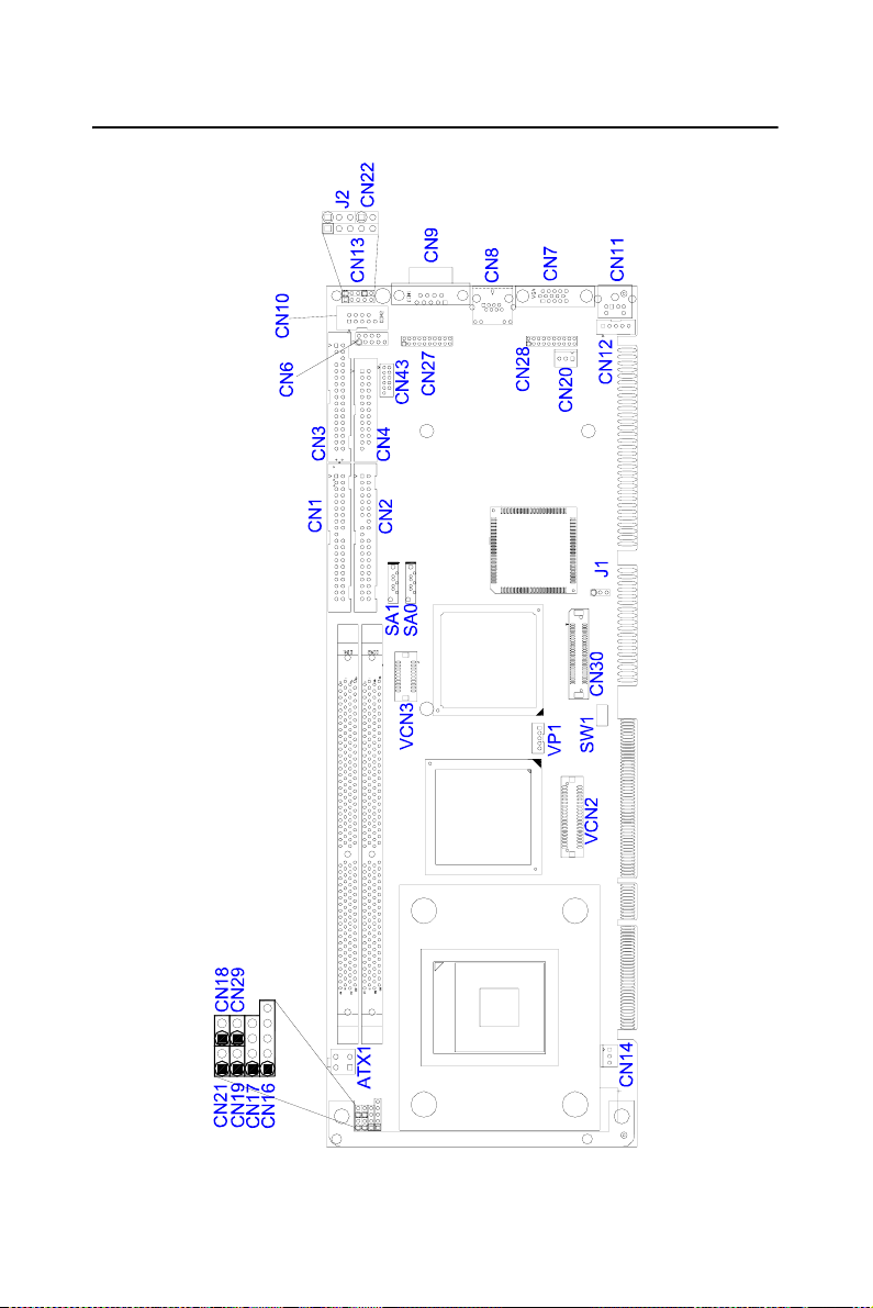
1.5 Board Layout: Jumper and Connector Location ............... 8
Figure 1.1:Jumper and Connector locations ................... 8
Figure 1.2:I/O Connectors .............................................. 9
Figure 1.3:SCSI daughter board ..................................... 9
1.6 PCA-6189 Block Diagram .............................................. 10
Figure 1.4:Block Diagram ............................................ 10
1.7 Safety Precautions ........................................................... 11
1.8 Jumper Settings ............................................................... 12
1.8.1 How to set jumpers ....................................................... 12
1.8.2 CMOS clear (J1) ........................................................... 12
Table 1.5:CMOS (J1).................................................... 12
1.8.3 Watchdog timer output (J2) .......................................... 12
Table 1.6:Watchdog timer output (J2).......................... 13
1.9 System Memory .............................................................. 13
1.9.1 CPU FSB and memory speed ....................................... 14
Table 1.7:CPU FSB and memory speed ....................... 14
1.10 Memory Installation Procedures ..................................... 14
1.11 Processor Installation ...................................................... 14
Chapter 2 Connecting Peripherals .................................18
2.1 Introduction ..................................................................... 18
2.2 1st & 2nd (CN1, CN2) IDE Connectors ......................... 18
2.3 Floppy Drive Connector (CN3)....................................... 19
2.4 Parallel Port (CN4).......................................................... 20
xiii
Page 14

2.5 USB Ports CN6, CN31, and CN32 ................................. 21
2.6 VGA Connector CN7 ...................................................... 22
2.7 LVDS connector VCN2 .................................................. 22
2.8 DVI connector VCN3...................................................... 23
2.9 Ethernet Connector (CN8 and CN34) ............................. 23
2.10 Serial Ports (COM1 : CN9; COM2 : CN10 ) .................. 24
2.11 PS/2 Keyboard/Mouse Connector (CN11/CN33) ........... 24
2.12 External Keyboard Connector (CN12)............................ 25
2.13 CPU Fan Connector (CN14) ........................................... 25
2.14 Front Panel Connectors (CN16, 17, 18, 19, 21&29) ....... 26
2.14.1 Power LED (CN16) ...................................................... 26
2.14.2 External speaker (CN17) .............................................. 26
2.14.3 Reset (CN18) ................................................................ 27
2.14.4 HDD LED (CN19)........................................................ 27
2.14.5 ATX soft power switch (CN21).................................... 27
2.14.6 SM Bus Connector (CN29)........................................... 27
2.15 ATX feature connector (CN20)....................................... 28
2.16 AC-97 Audio interface (CN43)....................................... 28
2.17 Serial ATA interface (SA0 and SA1).............................. 29
2.18 Connecting to SNMP-1000 remote manager .................. 29
2.19 Auxiliary 4-pin power connector (ATX1) ...................... 30
Chapter 3 Award BIOS Setup.........................................32
3.1 Introduction ..................................................................... 32
3.1.1 CMOS RAM Auto-backup and Restore ....................... 32
3.2 Entering Setup ................................................................. 33
Figure 3.1:Award BIOS Setup initial screen ................ 33
3.3 Standard CMOS Setup .................................................... 33
Figure 3.2:Standard CMOS features screen ................. 33
3.4 Advanced BIOS Features ................................................ 34
Figure 3.3:Advanced BIOS features screen.................. 34
3.4.1 CPU Features ................................................................ 34
3.4.2 Hard Disk Boot Priority................................................ 34
3.4.3 Virus Warning............................................................... 34
3.4.4 CPU L1 & L2 Cache, CPU L3 Cache .......................... 34
3.4.5 Quick Power On Self Test ............................................ 35
3.4.6 First/Second/Third Boot Device .................................. 35
3.4.7 Boot Other Device ........................................................ 35
3.4.8 Swap Floppy Drive ...................................................... 35
3.4.9 Boot UP Floppy Seek ................................................... 35
3.4.10 Boot Up NumLock Status............................................. 35
3.4.11 Gate A20 Option........................................................... 35
3.4.12 Typematic Rate Setting................................................. 35
3.4.13 Typematic Rate (Chars/Sec) ......................................... 35
PCA-6189 User’s Manual xiv
Page 15

3.4.14 Typematic Delay (msec) ............................................... 35
3.4.15 Security Option ............................................................. 36
3.4.16 APIC Mode................................................................... 36
3.4.17 MPS Version Control For OS ....................................... 36
3.4.18 OS Select For DRAM > 64MB .................................... 36
3.4.19 Report No FDD For WIN 95 ........................................ 36
3.4.20 Small Logo(EPA) Show ............................................... 36
3.5 Advanced Chipset Features............................................. 37
Figure 3.4:Advanced chipset features screen ............... 37
3.5.1 DRAM Timing Selectable ............................................ 37
3.5.2 CAS Latency Time ....................................................... 37
3.5.3 Active to Precharge Delay ............................................ 37
3.5.4 DRAM RAS# to CAS# Delay ..................................... 38
3.5.5 DRAM RAS# Precharge............................................... 38
3.5.6 DRAM Data Integrity Mode......................................... 38
3.5.7 System BIOS Cacheable............................................... 38
3.5.8 Video Bios Cacheable................................................... 38
3.5.9 Memory Hole At 15M-16M ......................................... 38
3.5.10 Delayed Transaction ..................................................... 38
3.5.11 Delay Prior to Thermal ................................................. 38
3.5.12 AGP Aperture Size (MB) ............................................. 39
3.5.13 Init Display First .......................................................... 39
3.5.14 On-Chip VGA............................................................... 39
3.5.15 On-Chip Frame Buffer Size.......................................... 39
3.5.16 Boot display .................................................................. 39
3.5.17 Panel Number ............................................................... 39
3.6 Integrated Peripherals...................................................... 40
Figure 3.5:Integrated peripherals .................................. 40
3.7 On-chip IDE Device........................................................ 40
Figure 3.6:On-Chip IDE Device ................................... 40
3.7.1 IDE DMA transfer access ............................................. 40
3.7.2 On-Chip IDE Device .................................................... 41
3.7.3 On-Chip Serial ATA ..................................................... 41
3.7.4 Serial ATA Port0/Port1 Mode ...................................... 41
3.7.5 IDE HDD Block Mode ................................................. 41
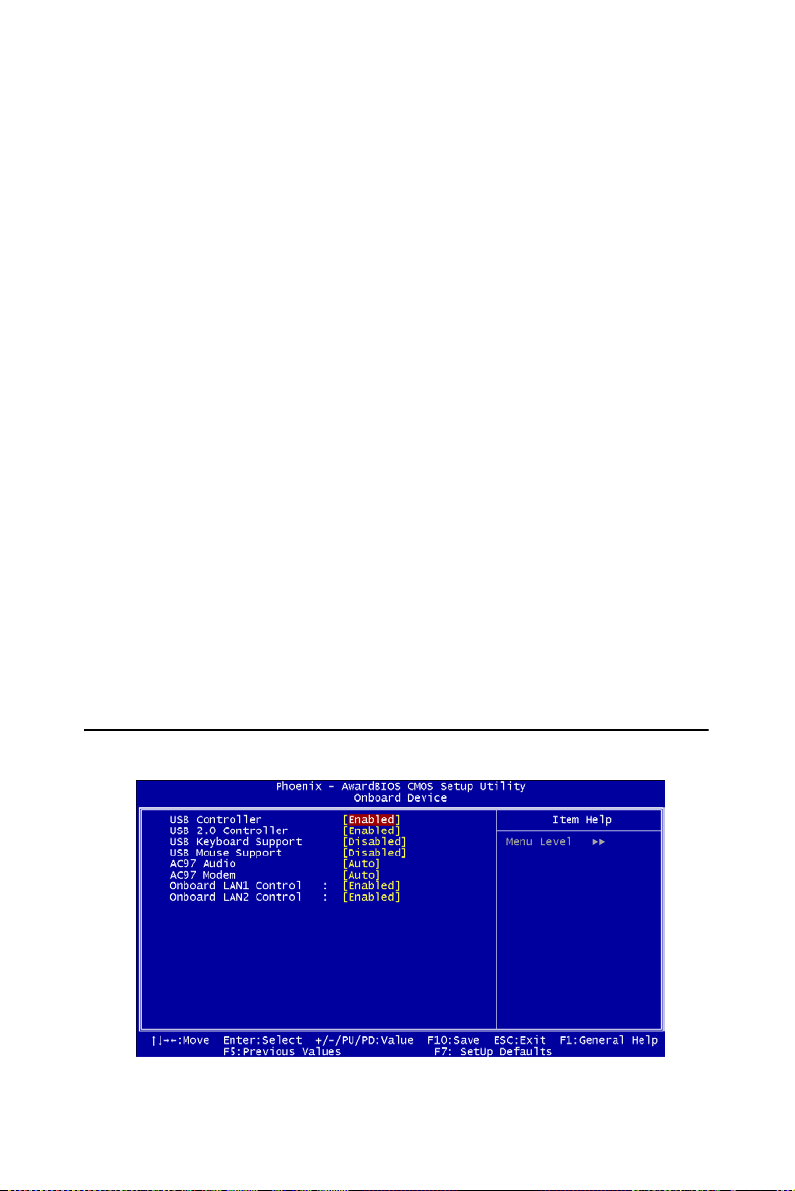
3.8 Onboard Device Menu .................................................... 41
Figure 3.7:Onboard Device........................................... 41
3.8.1 USB Controller ............................................................. 42
3.8.2 USB 2.0 Controller ....................................................... 42
3.8.3 USB Keyboard/Mouse Support .................................... 42
3.8.4 AC97 Audio .................................................................. 42
3.8.5 On-board LAN1 Control............................................... 42
3.8.6 On-board LAN2 Control............................................... 42
3.9 SuperIO Device ............................................................... 42
Figure 3.8:SuperIO Device ........................................... 42
xv
Page 16

3.9.1 On-board FDC Controller ............................................. 43
3.9.2 On-board Serial Port 1 .................................................. 43
3.9.3 On-board Serial Port 2 .................................................. 43
3.9.4 UART Mode Select ...................................................... 43
3.9.5 RxD, TxD Active .......................................................... 43
3.9.6 IR Transmission Delay ................................................. 43
3.9.7 UR2 Duplex Mode ........................................................ 43
3.9.8 Use IR Pins ................................................................... 43
3.9.9 On-board Parallel Port .................................................. 43
3.9.10 Parallel Port Mode ........................................................ 43
3.9.11 EPP Mode Select .......................................................... 44
3.9.12 ECP Mode Use DMA ................................................... 44
3.9.13 PWRON After PWR-FAIL........................................... 44
3.10 Power Management Setup............................................... 44
Figure 3.9:Power management setup screen (1)........... 44
3.10.1 ACPI function ............................................................... 44
3.10.2 Power Management ...................................................... 44
3.10.3 Video Off Method......................................................... 45
3.10.4 Video Off In Suspend .................................................. 45
3.10.5 Suspend Type................................................................ 45
3.10.6 Modem Use IRQ........................................................... 45
3.10.7 Soft-Off by PWR-BTTN .............................................. 45
3.10.8 CPU THRM-Throttling................................................. 45
3.10.9 Power On by LAN ........................................................ 46
3.10.10 Power On by Modem .................................................... 46
3.10.11 Power On by Alarm ...................................................... 46
3.10.12 Primary IDE (0,1) and Secondary IDE (0,1) ................ 46
3.10.13 FDD, COM, LPT PORT ............................................... 46
3.10.14 PCI PIRQ [A-D]# ........................................................ 46
3.11 PnP/PCI Configurations .................................................. 46
Figure 3.10:PnP/PCI configurations screen.................. 46
3.11.1 PNP OS Installed .......................................................... 47
3.11.2 Reset Configuration Data.............................................. 47
3.11.3 Resources Controlled By .............................................. 47
3.11.4 PCI/VGA Palette Snoop ............................................... 47
3.12 PC Health Status.............................................................. 47
3.12.1 CPU Warning Temperature .......................................... 47
Figure 3.11:PC health status screen .............................. 47
3.12.2 Current System Temp ................................................... 48
3.12.3 Current CPU Temperature ............................................ 48
3.12.4 Current CPUFAN Speed............................................... 48
3.12.5 VCORE, VBAT(V), 5VSB(V) ..................................... 48
3.12.6 Shutdown Temperature................................................. 48
3.13 Frequency/Voltage Control ............................................. 48
Figure 3.12:Spread Spectrum Control screen ............... 48
PCA-6189 User’s Manual xvi
Page 17

3.13.1 Auto-detect PCI CLK ................................................... 48
3.13.2 Spread Spectrum ........................................................... 48
3.14 Passwords and Settings ................................................... 49
3.14.1 Load Setup Defaults...................................................... 49
3.14.2 Set Supervisor Password............................................... 49
3.14.3 Set User Password ........................................................ 49
3.14.4 Save & Exit Setup......................................................... 49
3.14.5 Exit Without Saving...................................................... 49
Chapter 4 Chipset Software Install Utility.....................52
4.1 Before you begin ............................................................. 52
4.2 Introduction ..................................................................... 52
4.3 Windows XP Driver Setup .............................................. 53
Chapter 5 VGA Setup ......................................................58
5.1 Introduction ..................................................................... 58
5.2 Dynamic Video Memory Technology (DVMT) ............. 58
5.3 Windows XP Driver Setup .............................................. 59
Chapter 6 LAN Configuration ........................................64
6.1 Introduction ..................................................................... 64
6.2 Features ........................................................................... 64
6.3 Installation....................................................................... 65
6.4 Win XP Driver Setup (Intel 82541/82551) ..................... 65
Chapter 7 SCSI Setup & Configuration.........................70
7.1 Introduction ..................................................................... 70
7.2 Understanding SCSI....................................................... 71
7.3 SCSI IDs.......................................................................... 71
7.4 Terminating the SCSI Bus............................................ 72
7.5 Configuring the SCSI interface with SCSISelect............ 73
7.6 Starting SCSISelect ........................................................ 75
7.7 Using SCSI Disk Utilities ............................................... 79
7.8 Installation under Windows 2000 .................................. 80
7.9 Windows 9X Driver setup procedure.......................... 80
Chapter 8 USB 2.0 Configuration...................................86
8.1 Introduction ..................................................................... 86
8.2 Features ........................................................................... 86
8.3 Installation....................................................................... 86
Chapter 9 Onboard Security Setup ................................88
9.1 Introduction ..................................................................... 88
9.2 Windows XP Driver Setup .............................................. 89
9.3 Using the OBS Hardware Doctor Utility ........................ 91
Chapter 10 SATA RAID Setup .........................................94
xvii
Page 18

10.1 Introduction ..................................................................... 94
10.2 Entering Setup ................................................................. 94
Figure 10.1:RAID Setup initial screen ......................... 94
10.3 Array Configuration Utility............................................. 95
Figure 10.2:SATA RAID Setup Main Menu screen..... 95
10.3.1 Managing Arrays .......................................................... 95
10.3.2 Creating Arrays............................................................. 96
10.3.3 Adding/Removing a Bootable Array ............................ 96
10.3.4 Add/Delete Hotspares ................................................... 96
10.3.5 Initializing Disk Drives................................................. 96
10.3.6 Rebuilding Arrays......................................................... 97
10.4 Installing the driver ......................................................... 97
Appendix A Programming the watchdog .......................100
A.1 Programming the Watchdog Timer ............................... 100
A.1.1 Watchdog timer overview........................................... 100
A.1.2 Reset/ Interrupt selection ............................................ 100
A.1.3 Programming the Watchdog Timer ............................ 100
A.1.4 Example Program ....................................................... 103
Appendix B Pin Assignments ..........................................110
B.1 IDE Hard Drive Connector (CN1, CN2)....................... 110
Table B.1:IDE hard drive connector (CN1, CN2)...... 110
B.2 Floppy Drive Connector (CN3)..................................... 111
Table B.2:Floppy drive connector (CN3)................... 111
B.3 Parallel Port Connector (CN4) ...................................... 112
Table B.3:Parallel port connector (CN4) .................... 112
B.4 USB Connector (CN6) .................................................. 113
Table B.4:USB1/USB2 connector (CN6)................... 113
B.5 VGA Connector (CN7) ................................................. 113
Table B.5:VGA connector (CN7) ............................... 113
B.6 VCN2 LVD connector .................................................. 114
Table B.6:VCN2 LVDS connector............................. 114
B.7 VCN3 DVI connector.................................................... 115
Table B.7:VCN3 DVI connector ................................ 115
B.8 COM1/COM2 RS-232 Serial Port (CN9, CN10).......... 115
Table B.8:COM1/2 RS-232 serial port (CN9/10)....... 115
B.9 PS/2 Keyboard/Mouse Connector (CN11).................... 116
Table B.9:PS/2 keyboard/mouse connector (CN11)... 116
B.10 External Keyboard Connector (CN12).......................... 116
Table B.10:External keyboard connector (CN12) ...... 116
B.11 Power LED (CN16)....................................................... 116
Table B.11: CPU Fan Power Connector (CN14)........ 116
B.12 Power LED (CN16)....................................................... 117
Table B.12:Power LED (CN16) ................................. 117
PCA-6189 User’s Manual xviii
Page 19

B.13 External Speaker Connector (CN17)............................. 117
Table B.13:External Speaker Connector (CN17) ....... 117
B.14 Reset Connector (CN18) ............................................... 118
Table B.14:Reset connector (CN18)........................... 118
B.15 ATX Feature Connector (CN20)................................... 118
Table B.15:HDD LED connector (CN19) .................. 118
B.16 ATX Feature Connector (CN20)................................... 119
Table B.16:ATX Feature Connector (CN20) ............. 119
B.17 ATX Soft Power Switch (CN21) .................................. 119
Table B.17:ATX soft power switch (CN21)............... 119
B.18 H/W Monitor Alarm (CN22)......................................... 120
Table B.18:H/W Monitor alarm (CN22) .................... 120
B.19 SM Bus Connector (CN29) .......................................... 120
Table B.19:SM bus onnector (CN29) ......................... 120
B.20 Audio Interface (CN43) ................................................ 121
Table B.20:Audio Interface(CN 43) ........................... 121
B.21 LCD Inverter power connectore (VP1)......................... 121
Table B.21:LCD inverter power connector (CN 20) .. 121
B.22 System I/O Ports............................................................ 122
Table B.22:System I/O ports ...................................... 122
B.23 DMA Channel Assignments.......................................... 123
Table B.23:DMA channel assignments ...................... 123
B.24 Interrupt Assignments ................................................... 123
Table B.24:Interrupt assignments ............................... 123
B.25 1st MB Memory Map.................................................... 124
Table B.25:1st MB memory map ............................... 124
B.26 PCI Bus Map ................................................................. 124
Table B.26:PCI bus map ............................................. 124
xix
Page 20

PCA-6189 User’s Manual xx
Page 21

CHAPTER
General Information
1
1
Page 22

Chapter 1 Hardware Configuration
1.1 Introduction
The PCA-6189 is designed with Intel® 855GME chipset and 6300ESB
(I/O controller) to support the Intel® Pentium® M / Celeron® M processor, high speed DDR333 memory, and high performance I/O functions
such as dual Gigabit Ethernet ports, Serial/parallel ATA ports, and a PCIX (64-bit / 66Mhz) bus. With the compliance with PICMG 1.0 specification, PCA-6189 can be used with wide choice of existing PCI/ISA backplanes to meet versatile requirements of industrial applications.
The PCA-6189 is designed to deliver high performance but low thermal
profile best for industrial embedded applications. It uses Intel's long-life
855GME and 6300ESB chipset, with the socket 479 it can supports vary
on the Pentium® M and Celeron® M processor by different applications.
It has 2 DIMM sockets and supports ECC (error checking and correction)
function for best reliability. It accepts up to 2GB DDR 333/266 SDRAM
memory, enough for most of applications. PCA-6189 could support dual
Giga LAN with the Gigabit Ethernet ports controller -- Intel® 82541
which is connected to the 32-bit PCI bus of the 6300ESB I/O controller.
With the 855GME integrated graphic controller PCA-6189 provides one
VGA display connector one LVDS and one DVI interface for panel display. Two serial ATA ports (up to 150MB/s)which can support RAID 0,1
functions and allows the use of thin and long SATA cables for storage
devices, eliminating the cabling issue inside an industrial grade chassis.
In addition, the PCA-6189 also provides most of the popular I/O interfaces such as four USB 2.0 ports, AC-97 audio interface, 2 RS-232 ports,
one enhanced parallel port and floppy disk interface.
The PCA-6189 is designed with reliability considerations to be suitable
for industrial environments. A specially designed heat-sink is attached to
the main chips to keep them cool and to extend the operating temperature
to 60 degree Celsius. The CMOS data backup and restore function protects the BIOS setup data from loss due to battery failure. A 256-level
watchdog timer prevents the system from hanging up if a program cannot
be executed normally. A remote management port allows users to monitor the system healthy status and control the system remotely through the
standard SNMP/HTTP protocols when used with Advantech's SNMP1000 Intelligent System Manager.
PCA-6189 User’s Manual 2
Page 23

Note: Some of the features mentioned above are not
available with all models. For more information
about the specifications of a particular model,
see Table 1.1 : Comparison table and Section
1.3: Specifications.
1.2 Features
1. Supports FSB 400 MHz low thermal profile Intel® Pentium® M
processor or Intel® Celeron® M processor
2. Supports 2 Serial-ATA devices with Software RAID 0 or 1 functions
3. Supports DDR 200/266/333 SDRAM up to 2GB
4. Optional onboard Adaptec AIC-7899 dual channel Ultra160 SCSI
up to 160MB/sec.
5. Onboard integrated VGA controller supports LVDS and DVI interface
6. 64-bit, 66MHz PCI-X
7. Supports 10/100/1000Base-T Ethernet
8. Remote management with SNMP-1000-B1
1.3 Specifications
1.3.1 System
• CPU: Intel® socket 479 Celeron® M up to 1.5 GHz, Pentium® M up
to 2.0 GHz, FSB 400 MHz
• L2 Cache: CPU built-in 512/1024/2048 KB full-speed L2 cache
• BIOS: Award Flash BIOS (4Mb Flash Memory)
• System Chipset: Intel 855GME + 6300ESB
• SATA/EIDE hard disk drive interface: Supports up to two indepen-
dent Serial ATA hard drives (up to 150MB/s) with software RAID 0 or
1 functions, as well as two IDE hard disk drives, or four enhanced IDE
devices. Supports PIO mode 4 (16.67 MB/s data transfer rate) and ATA
33/66/100 (33/66/100MB/s data transfer rate.)
3
Page 24

• Floppy disk drive interface: Supports up to two floppy disk drives,
5¼" (360 KB and 1.2 MB) and/or 3½" (720 KB, 1.44 MB). BIOS
enabled/disabled
1.3.2 Memory
• RAM: Up to 2 GB in two 184-pin DIMM sockets. Supports DDR266/
333 SDRAM
1.3.3 Input/Output
• Bus interface: PICMG 1.0 compliant PCI/ISA bus interface
• Enhanced parallel port: Configurable to LPT1, LPT2, LPT3, or dis-
abled. Standard DB-25 female connector provided. Supports EPP/SPP/
ECP
• Serial ports: Two RS-232 ports with 16C550 UARTs (or compatible)
with 16-byte FIFO buffer. Supports speeds up to 115.2 Kbps. Ports can
be individually configured to COM1, COM2 or disabled
• Keyboard and PS/2 mouse connector: One 6-pin mini-DIN connector
is located on the mounting bracket for easy connection to a keyboard or
PS/2 mouse. An on board keyboard pin header connector is also available
• ISA bus: Supports ISA without DMA. PCI-to-ISA bridge: ITE IT8888
• AC-97 Audio: PCA-6189 can provide audio function with the optional
audio extension module PCA-AUDIO-00A1
• USB ports: PCA-6189 supports up to four USB 2.0 ports with trans-
mission rates up to 480Mbps; available on the I/O bracket (dual layer
brackets only) or through the two-USB-port cable (P/N: 1700100170)
for single layer version. With the dual layer versions, users can choose
between CN32 on the I/O bracket or the on-board connector CN6,
depending on their applications. For example, users can link CN6 to
the front side panel thru the USB cable. Please note that users can't use
CN32 on I/O bracket and CN6 at the same time. Users must set S1 and
S2 (on the back side of the CPU card) correctly for the USB port configuration they are using. Please refer to section 2.5 for switch settings.
1.3.4 VGA interface
• Controller: Intel 855GME chipset integrated
• Display memory: Share system memory up to 64 MB, BIOS selectable
• Resolution: VGA port: 2048 x 1536, up to 75 Hz
PCA-6189 User’s Manual 4
Page 25

LVDS connector, dual channel: 25 MHz to 112 MHz
DVI connector: 2048 x 1536, 75 MHz
1.3.5 Ethernet LAN
• Supports single 10/100Base-T networking or single/dual10/100/
1000Base-T Ethernet networking
• Controller:
• Single 10/100Base-T: Intel 82551QM
• Single 10/100/1000Base-T: Intel 82541GI(PCI)
• Dual 10/100/1000Base-T: Two Intel 82541GI (PCI)
1.3.6 Ultra 160 SCSI
• Provides dual channel Ultra 160 SCSI interface
• Chipset: Adaptec AIC7899
1.3.7 Industrial features
• Watchdog timer: Can generate a system reset or IRQ11. The watch-
dog timer is programmable, with each unit equal to one second or one
minute (255 levels). You can find programming detail in Appendix A
1.3.8 Mechanical and environmental specifications
• Operating temperature: 0° ~ 60° C (32° ~ 140° F, depending on CPU)
• Storage temperature: -20°~ 70° C (-4° ~ 158° F)
• Humidity: 20 ~ 95% non-condensing
• Power supply voltage: +5 V, ±12 V
• Power consumption: Typical : +5V:6.53A, +12V:4.57A (Intel Pen-
tium® M 1.8 GHz with 400 MHz FSB, 512 MB DDR 333 SDRAM)
• Board size: 338 x 122 mm (13.3" x 4.8")
• Board weight: 0.5 kg (1.2 lb)
1.4 Jumpers and Connectors
Connectors on the PCA-6189 single board computer link it to external
devices such as hard disk drives and a keyboard. In addition, the board
has a number of jumpers used to configure your system for your application.
The tables below list the function of each of the board jumpers and connectors. Later sections in this chapter give instructions on setting jump-
5
Page 26

ers. Chapter 2 gives instructions for connecting external devices to your
single board computer.
Table 1.1: Jumpers
Label
J1 CMOS Clear
J2 Watchdog timer output selection
Function
Table 1.2: Connectors
Label
CN1 Primary IDE connector
CN2 Secondary IDE connector
CN3 Floppy drive connector
CN4 Parallel port
CN6 USB port (share with CN32)
CN7 VGA connector
VCN2 LVDS connector
VCN3 DVI connector
CN8 Ethernet connector 1
CN9 Serial port: COM1
CN10 Serial port: COM2
CN11 PS/2 keyboard and mouse connector
CN12 External keyboard connector
CN13 Reserved
CN14 CPU FAN connector
CN16 Power LED
CN17 External speaker
CN18 Reset connector
CN19 HDD LED connector
CN20 ATX feature connector
CN21 ATX soft power switch (PS_ON)
Function
PCA-6189 User’s Manual 6
Page 27

Table 1.2: Connectors
CN22 HW Monitor Alarm
Close: Enable OBS Alarm
Open: Disable OBS Alarm
CN27 Extension I/O board connector
CN28 Extension I/O board connector
CN29 SM BUS Connector
PIN1: SMB_DATA
PIN2: SMB_CLOCK
CN30 Extension PCI connector (for SCSI daughter board)
CN31 USB port 0,1
CN32 USB port 2,3
CN34 Ethernet connector 2
CN43 AC97 Link connector
CN44 CF Socket (On Back Side)
SA0 Serial ATA0
SA1 Serial ATA1
ATX1 ATX 12 V Auxillary power connector
VP1 LCD inverter power connector
Notice: The 4-pin ATX 12V power connector "ATX1" must be connected to the
power supply to provide adequate power to the CPU card. Otherwise system might
be unstable.
Table 1.3: SCSI Daughter Board Connectors
CN1 Channel A 68-pin Ultra 160 SCSI Connector
CN2 Channel B 68-pin Ultra 160 SCSI Connector
CN3 Channel B 50-pin Ultra Wide SCSI Connector
Table 1.4: On Board Switch
S1,S2 USB connector(CN6 or CN32) selection switch
SW1 PCI bus selection switch
7
Page 28
1.5 Board Layout: Jumper and Connector Location
Figure 1.1: Jumper and Connector locations
PCA-6189 User’s Manual 8
Page 29
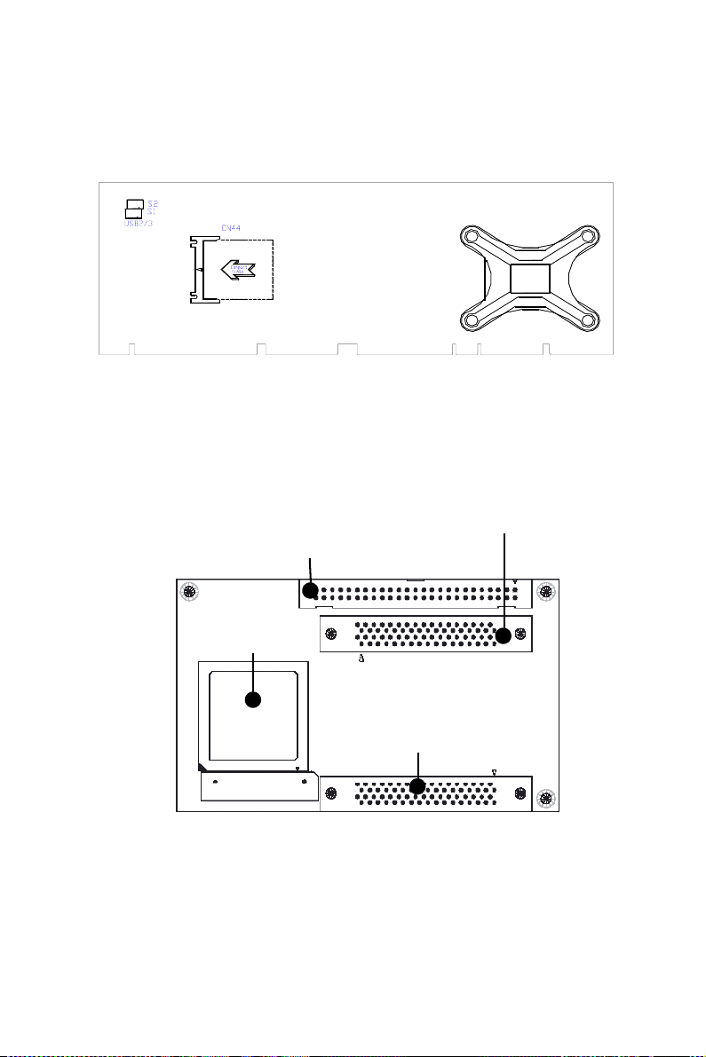
Figure 1.2: I/O Connectors
68 Pin for Ultra 160
50 Pin for Ultra wide SCSI
Adaptec
AIC-7899
68 Pin for Ultra 160
Figure 1.3: SCSI daughter board
9
Page 30

1.6 PCA-6189 Block Diagram
Figure 1.4: Block Diagram
PCA-6189 User’s Manual 10
Page 31

1.7 Safety Precautions
Warning! Always completely disconnect the power cord
from your chassis whenever you work with the
hardware. Do not make connections while the
power is on. Sensitive electronic components
can be damaged by sudden power surges. Only
experienced electronics personnel should open
the PC chassis.
Caution! Always ground yourself to remove any static
charge before touching the single board computer. Modern electronic devices are very sensitive to static electric charges. As a safety
precaution, use a grounding wrist strap at all
times. Place all electronic components on a
static-dissipative surface or in a static-shielded
bag when they are not in the chassis.
Caution! The computer is provided with a battery-pow-
ered Real-time Clock circuit. There is a danger
of explosion if battery is incorrectly replaced.
Replace only with same or equivalent type recommended by the manufacturer. Discard used
batteries according to manufacturer's instructions.
Notice: Before install your PCA-6189 into a chassis, make sure that all components
on both sides of the CPU card do not touch any metal parts, especially the chassis
wall and add-on card at the adjacent slot.
11
Page 32

1.8 Jumper Settings
This section provides instructions on how to configure your single board
computer by setting the jumpers. It also includes the single board computer's default settings and your options for each jumper.
1.8.1 How to set jumpers
You can configure your single board computer to match the needs of your
application by setting the jumpers. A jumper is a metal bridge that closes
an electrical circuit. It consists of two metal pins and a small metal clip
(often protected by a plastic cover) that slides over the pins to connect
them. To “close” (or turn ON) a jumper, you connect the pins with the
clip. To “open” (or turn OFF) a jumper, you remove the clip. Sometimes
a jumper consists of a set of three pins, labeled 1, 2, and 3. In this case
you connect either pins 1 and 2, or 2 and 3. A pair of needle-nose pliers
may be useful when setting jumpers.
1.8.2 CMOS clear (J1)
The PCA-6189 single board computer contains a jumper that can erase
CMOS data and reset the system BIOS information. Normally this
jumper should be set with pins 1-2 closed. If you want to reset the CMOS
data, set J1 to 2-3 closed for just a few seconds, and then move the jumper
back to 1-2 closed. This procedure will reset the CMOS to its default set-
ting.
Table 1.5: CMOS (J1)
Function Jumper Setting
* Keep CMOS data
1 -2 closed
Clear CMOS data
2 3 closed
* default setting
1.8.3 Watchdog timer output (J2)
The PCA-6189 contains a watchdog timer that will reset the CPU or send
a signal to IRQ11 in the event the CPU stops processing. This feature
means the PCA-6189 will recover from a software failure or an EMI
problem. The J2 jumper settings control the outcome of what the computer will do in the event the watchdog timer is tripped.
PCA-6189 User’s Manual 12
Page 33

Table 1.6: Watchdog timer output (J2)
Function
Jumper Setting
IRQ11
* Reset
* default setting
1
1-2 closed
1
2-3 closed
Note: The interrupt output of the watchdog timer is a
low level signal. It will be held low until the
watchdog timer is reset.
1.9 System Memory
The PCA-6189 has two sockets for 184-pin dual inline memory modules
(DIMMs).
All these sockets use 2.5 V unbuffered double data rate synchronous
DRAMs (DDR SDRAM). They are available in capacities of 128, 256,
512 and 1024 MB. The sockets can be filled in any combination with
DIMMs of any size, giving a total memory size between 128 MB and 2
GB.
13
Page 34

1.9.1 CPU FSB and memory speed
The PCA-6189 can accept DDR SDRAM memory chips without parity.
Also note: The PCA-6189 accepts PC2100 (DDR266), PC2700 (DDR
333) and DDR SDRAM, depending on the CPU front side bus frequency
(FSB). Please refer to the table below for the relationship between the
CPU FSB and memory speed.
Table 1.7: CPU FSB and memory speed
Memory
Speed
DDR400 Pentium M or
DDR333 Pentium M or
DDR266 Pentium M or
Processor FSB frequency Memory speed
Outcome
400 MHz 333 MHz
Celeron M
400 MHz 333 MHz
Celeron M
400 MHz 266 MHz
Celeron M
The PCA-6189 supports ECC (error checking and correction), and memory modules with 9 SDRAM chips/side support ECC.
1.10 Memory Installation Procedures
To install DIMMs, first make sure the two handles of the DIMM socket
are in the "open" position. i.e. The handles lean outward. Slowly slide the
DIMM module along the plastic guides on both ends of the socket. Then
press the DIMM module right down into the socket, until you hear a
click. This is when the two handles have automatically locked the memory module into the correct position of the DIMM socket. To remove the
memory module, just push both handles outward, and the memory module will be ejected by the mechanism in the socket.
1.11 Processor Installation
The CPU on the board must have a fan or heat sink attached, to prevent
overheating.
PCA-6189 User’s Manual 14
Page 35

Warning: Without a fan or heat sink, the CPU will over-heat
and cause damage to both the CPU and the single
board computer. To install a CPU, first turn off your
system and remove its cover. Locate the processor
socket 479.
1. To open the socket, turn the socket screw clockwise as far as it will go.
2. Place the CPU in the empty socket and then follow the instructions that
came with the CPU. If you have no instructions, complete the following
procedure:
- Carefully align the CPU on top of the socket, making sure the
corner pin patterns of the CPU match the patterns on the socket.
- Gently place the CPU on top of the socket. It should insert easily.
If it does not insert easily, check that the socket screw is turned clockwise
as far as possible.
3. After the CPU has been inserted, turn the screw counter-clockwise as
far as it will go to lock the CPU into position. The top plate of the socket
should slide up into the locked position. You will feel some resistance
against the screw as the CPU pins tighten in the socket. This is normal
and will not damage the CPU. Turn the screw counter-clockwise as far as
it will go.
15
Page 36

PCA-6189 User’s Manual 16
Page 37

2
CHAPTER
Connecting Peripherals
17 Chapter 2
Page 38

Chapter 2 Connecting Peripherals
2.1 Introduction
You can access most of the connectors from the top of the board while it
is installed in the chassis. If you have a number of cards installed or have
a packed chassis, you may need to partially remove the card to make all
the connections.
2.2 1st & 2nd (CN1, CN2) IDE Connectors
CN1
CN2
You can attach up to four IDE (Integrated Drive Electronics) drives to the
PCA-6189’s built-in controller. The primary (CN1) and secondary (CN2)
connectors can each accommodate two drives.
Wire number 1 on the cable is red or blue and the other wires are gray.
Connect one end to connector CN1 or CN2 on the single board computer.
Make sure that the red/blue wire corresponds to pin 1 on the connector (in
the upper right hand corner). See Chapter 1 for help finding the connector.
Unlike floppy drives, IDE hard drives can connect in either position on
the cable. If you install two drives to a single connector, you will need to
set one as the master and the other as the slave. You do this by setting the
jumpers on the drives. If you use just one drive per connector, you should
set each drive as the master. See the documentation that came with your
drive for more information.
PCA-6189 User’s Manual 18
Page 39

Connect the first hard drive to the other end of the cable. Wire 1 on the
cable should also connect to pin 1 on the hard drive connector, which is
labeled on the drive circuit board. Check the documentation that came
with the drive for more information.
Connect the second hard drive to the remaining connector (CN2 or CN1),
in the same way as described above.
2.3 Floppy Drive Connector (CN3)
CN3
You can attach up to two floppy disk drives to the PCA-6189's on board
controller. You can use 3.5" (720 KB, 1.44 MB) drives.
The single board computer comes with a 34-pin daisy-chain drive connector cable. On one end of the cable is a 34-pin flat-cable connector. On
the other end are two sets of 34-pin flat-cable connector (usually used for
3.5" drives). The set on the end (after the twist in the cable) connects to
the A: floppy drive. The set in the middle connects to the B: floppy drive.
19 Chapter 2
Page 40

2.4 Parallel Port (CN4)
CN4
The parallel port is normally used to connect the single board computer to
a printer. The PCA-6189 includes an onboard parallel port, accessed
through a 26-pin flat-cable connector, CN4. The card comes with an
adapter cable which lets you use a traditional DB-25 connector. The cable
has a 26-pin connector on one end and a DB-25 connector on the other,
mounted on a retaining bracket. The bracket installs at the end of an
empty slot in your chassis, giving you access to the connector.
The parallel port is designated as LPT1, and can be disabled or changed
to LPT2 or LPT3 in the system BIOS setup.
To install the bracket, find an empty slot in your chassis. Unscrew the
plate that covers the end of the slot. Screw in the bracket in place of the
plate. Next, attach the flat-cable connector to CN4 on the CPU card. Wire
1 of the cable is red or blue, and the other wires are gray. Make sure that
wire 1 corresponds to pin 1 of CN4. Pin 1 is on the upper right side of
CN4.
PCA-6189 User’s Manual 20
Page 41

2.5 USB Ports CN6, CN31, and CN32
The PCA-6189 provides up to four ports for the USB (Universal Serial
Bus) interface, which gives complete Plug & Play and hot swapping for
up to 127 external devices.The USB interface complies with USB Specification Rev. 2.0, supports transmission rate up to 480 Mbps and is fuseprotected. The USB interface can be disabled in the system BIOS setup.
Connector CN31 connects to USB ports 0 and 1, while CN6 and CN32
share ports 2 and 3. Users can choose to use either CN6 or CN32 for ports
2 and 3 by setting the hyper-miniature DIP switch .To set the switch, see
the note below.
CN6
Note: To enable CN6, turn on pins 3 and 4 of S1 and
S2, and also turn off pins 1 and 2. To enable
CN32 (for USB ports 3 and 4 of the dual layer
bracket) turn on pin 1 and 2 of S1 and S2, and
also turn off pins 3 and 4. Any other DIP switch
setup for the USB function will be unstable.
21 Chapter 2
Page 42

2.6 VGA Connector CN7
CN7
The PCA-6189 includes a VGA interface that can drive conventional
CRT displays. CN7 is a standard 15-pin D-SUB connector commonly
used for VGA. Pin assignments for CRT connector CN7 are detailed in
Appendix B.
2.7 LVDS connector VCN2
The PCA-6189 provides a LVDS interface that supports 18-bit LCD panels. Pin assignments for the LVDS connector VCN2 are detailed in
Appendix B.
PCA-6189 User’s Manual 22
Page 43

2.8 DVI connector VCN3
The VCN3 provides a DVI interface that supports DVI display. This connector should be used with a 20-pin DVI cable (p/n: 1700000821) Pin
assignments for the VCN3 are detailed in Appendix B.
2.9 Ethernet Connector (CN8 and CN34)
The PCA-6189 is equipped with single/dual high-performance 32-bit
PCI-bus Ethernet interface, which is fully compliant with IEEE 802.3/u
10/100Mbps CSMA/CD and IEEE 802.3ab 1000Base-T standards. It is
supported by all major network operating systems and is 100% Novell
NE-2000 compatible. An onboard RJ-45 jack provides convenient 10/
100Base-T or 10/100/1000Base-T RJ-45 operation.
23 Chapter 2
Page 44

2.10 Serial Ports (COM1 : CN9; COM2 : CN10 )
The PCA-6189 offers two serial ports, CN9 as COM1 and CN10 as
COM2. These ports can connect to serial devices, such as a mouse or a
printer, or to a communications network.
The IRQ and address ranges for both ports are fixed. However, if you
want to disable the port or change these parameters later, you can do this
in the system BIOS setup.
Different devices implement the RS-232 standard in different ways. If
you are having problems with a serial device, be sure to check the pin
assignments for the connector.
2.11 PS/2 Keyboard/Mouse Connector (CN11/CN33)
CN11
The 6-pin mini-DIN connector (CN11) on the card mounting bracket provides connection to a PS/2 keyboard or a PS/2 mouse. CN11 can also be
connected to an adapter cable (P/N: 1700060202, available from Advantech) for connecting to both a PS/2 keyboard and a PS/2 mouse.
PCA-6189 User’s Manual 24
Page 45

2.12 External Keyboard Connector (CN12)
In addition to the PS/2 mouse/keyboard connector on the PCA-6189's
rear plate, there is also an extra onboard external keyboard connector.
This gives system integrators greater flexibility in designing their systems.
2.13 CPU Fan Connector (CN14)
CN12
CN14
If fan is used, this connector supports cooling fans of 500mA (6W) or
less.
25 Chapter 2
Page 46

2.14 Front Panel Connectors (CN16, 17, 18, 19, 21&29)
There are several external switches to monitor and control the PCA-6189
CN21
CN19
CN17
CN16
CN18
CN29
2.14.1 Power LED (CN16)
CN16 is a 5-pin connector for the power on LED. Refer to Appendix B
for detailed information on the pin assignments. If a PS/2 or ATX power
supply is used, the system's power LED status will be as indicated below:
Table 2.1: PS/2 or ATX power supply LED status
Power mode LED (PS/2 power) LED (ATX power)
System On On On
System Suspend Fast flashes Fast flashes
System Off Off Slow flashes
2.14.2 External speaker (CN17)
CN17 is a 4-pin connector for an external speaker. If there is no external
speaker, the PCA-6189 provides an onboard buzzer as an alternative. To
enable the buzzer, set pins 3-4 as closed
PCA-6189 User’s Manual 26
Page 47

2.14.3 Reset (CN18)
Many computer cases offer the convenience of a reset button. Connect the
wire from the reset button.
1
2.14.4 HDD LED (CN19)
You can connect an LED to connector CN19 to indicate when the HDD is
active.
1
2.14.5 ATX soft power switch (CN21)
If your computer case is equipped with an ATX power supply, you should
connect the power on/off button on your computer case to CN21. This
connection enables you to turn your computer on and off.
2.14.6 SM Bus Connector (CN29)
This connector is reserved for Advantech's SNMP-1000 HTTP/SNMP
Remote System Manager. The SNMP-1000 allows users to monitor the
internal voltages, temperature and fans from a remote computer through
an Ethernet network.
CN29 can be connected to CN19 of SNMP-1000. Please be careful about
the pin assignments, pin 1 must be connected to pin 1 and pin2 to pin 2 on
both ends of cable.
27 Chapter 2
Page 48

2.15 ATX feature connector (CN20)
CN20
Connect to the CN1 on the Advantech backplane to enable the ATX function, 5V stand-by.
2.16 AC-97 Audio interface (CN43)
CN43
The PCA-6189 provides AC-97 audio through PCA-AUDIO-00A1
module from Advantech.
PCA-6189 User’s Manual 28
Page 49

2.17 Serial ATA interface (SA0 and SA1)
SA0 & SA1
In addition to the two EIDE interfaces (up to four devices), the PCA-6189
features high performance serial ATA interface (up to 150MB/s) which
eases cabling to hard drives with thin and long cables.
2.18 Connecting to SNMP-1000 remote manager
Use the 6-pin to 8-pin cable to connect the single board computer to
SNMP-1000. This cable comes with the SNMP-1000.
PIN 1
CN21 CN18
CN19 CN29
CPU Card
CN19
PIN 1
SNMP-1000
29 Chapter 2
Page 50

2.19 Auxiliary 4-pin power connector (ATX1)
To ensure the sufficiency of power supply for Pentium M or Celeron M
single board computer, one auxiliary 4 pin power connector is available
on PCA-6189. This connector must be connected to the power supply,
otherwise system might be unstable.
PCA-6189 User’s Manual 30
Page 51

Award BIOS Setup
CHAPTER
3
31 Chapter 3
Page 52

Chapter 3 Award BIOS Setup
3.1 Introduction
Award’s BIOS ROM has a built-in setup program that allows you to modify the basic system configuration. This type of information is stored in
battery-backed memory (CMOS RAM) so that it retains the setup information when the power is turned off.
3.1.1 CMOS RAM Auto-backup and Restore
The CMOS RAM is powered by an onboard button cell battery. When
you finish BIOS setup, the data in CMOS RAM will be automatically
backed up to Flash ROM. If operation in a harsh industrial environment
causes a soft error, BIOS will recheck the data in CMOS RAM and automatically restore the original data in Flash ROM to CMOS RAM for
booting.
Note: If you intend to change the CMOS setting with-
out restoring the previous backup, you have to
click on "DEL" within two seconds of the
"CMOS checksum error..." display screen message appearing. Then enter the "Setup" screen
to modify the data. If the "CMOS checksum
error..." message appears again and again,
please check to see if you need to replace the
battery in your system.
PCA-6189 User’s Manual 32
Page 53

3.2 Entering Setup
Turn on the computer and press <Del> to enter the BIOS setup.
Figure 3.1: Award BIOS Setup initial screen
3.3 Standard CMOS Setup
Choose the Standard CMOS Features option from the initial setup screen
menu to display the screen below. This menu allows you to configure system components such as date, time, hard disk drive, floppy drive, display,
and memory.
Figure 3.2: Standard CMOS features screen
33 Chapter 3
Page 54

3.4 Advanced BIOS Features
The Advanced BIOS Features screen appears when you choose the
Advanced BIOS Features item from the initial setup screen menu. Use
this screen to configure the PCA-6189 according to your particular
requirements. Below are some major items that are provided in the
Advanced BIOS Features screen. A quick booting function is provided
for your convenience. Simply enable the Quick Booting item to save
yourself valuable time.
Figure 3.3: Advanced BIOS features screen
3.4.1 CPU Features
The CPU Features allows you to adjust the value of Thermal Monitors 1
and 2 with the BUS ratio and BUS VID settings. Using this setting, you
can choose to lower the CPU speed for a fixed length of time when the
CPU temperature gets too high. The choices are 4 Min, 8 Min, 16 Min,
and 32 Min.
3.4.2 Hard Disk Boot Priority
Use this setting to select the hard disk boot device priorities.
3.4.3 Virus Warning
Use this setting to enable virus warning. The choices are Enabled and
Disabled.
3.4.4 CPU L1 & L2 Cache, CPU L3 Cache
Enabling this feature speeds up memory access. The choices are Enabled
or Disabled.
PCA-6189 User’s Manual 34
Page 55

3.4.5 Quick Power On Self Test
This setting allows the system to skip certain tests while booting. This
will decrease the time needed to boot the system.
3.4.6 First/Second/Third Boot Device
The BIOS will load the OS with the devices in the sequence selected. The
sequence includes: Floppy, LS120, HDD-0, SCSI, CDROM, HDD-1,
HDD-2, HDD-3, ZIP100, USB-FDD, USB-ZIP, USBCDROM, USBHDD, LAN, and Disabled.
3.4.7 Boot Other Device
Use this option to choose another device to boot. The choices are
Enabled or Disabled.
3.4.8 Swap Floppy Drive
If the system has two floppy drives, choose Enabled to assign physical
drive B to logical drive A and vice-versa. The choices are Enabled or Dis-
abled.
3.4.9 Boot UP Floppy Seek
Select the command Disabled to speed the boot up. Select Enabled to
search disk drives during boot up.
3.4.10 Boot Up NumLock Status
This feature selects the power on state for NumLock. The choices are Off
and On.
3.4.11 Gate A20 Option
Normal: A pin in the keyboard controller controls Gate A20.
Fast (Default): The chipset controls GateA20.
3.4.12 Typematic Rate Setting
The typematic rate is the rate key strokes repeat as determined by the keyboard controller. The commands are Enabled and Disabled. Enabling
allows the typematic rate and delay to be selected.
3.4.13 Typematic Rate (Chars/Sec)
BIOS accepts the following input values (characters/second) for typematic rate: 6, 8, 10, 12, 15, 20, 24, 30.
3.4.14 Typematic Delay (msec)
Typematic delay is the time interval between the appearance of two consecutive characters, when holding down a key. The input values for this
category are: 250, 500, 750, 1000 (milliseconds).
35 Chapter 3
Page 56

3.4.15 Security Option
Choose an option for this setting to have the system prompt for a password every time the system boots or only when you enter setup.
System: The system will not boot and access to setup will be denied if the
correct password is not entered at the prompt.
Setup: The system will boot, but access to Setup will be denied if the correct password is not entered at the prompt.
Note: To disable security, select “PASSWORD SET-
TING” in the main menu. At this point, you will
be asked to enter a password. Simply press
<Enter> to disable security. When security is
disabled, the system will boot, and you can
enter Setup freely.
3.4.16 APIC Mode
Use this setting to enable the APIC mode. The choices are Disabled or
Enabled.
3.4.17 MPS Version Control For OS
This function reports if an FDD is available for Windows 95. The selections are 1.1 or 1.4.
3.4.18 OS Select For DRAM > 64MB
Select OS2 only if you are running OS/2 operating system with greater
than 64MB of RAM on the system. Commands are Non-OS2 or OS2.
3.4.19 Report No FDD For WIN 95
This setting determines if the BIOS should report the absence of a floppy
disk drive to Windows 95. When set to Ye s, the BIOS will assign IRQ 6 to
another device. This allows computers with no floppy disk drives to boot
into Windows 95 normally. When set to No, Windows 95 will detect the
absence of the floppy disk drive and halt the system with an error message. Please note that this BIOS feature has no relevance in other operating systems. Only Windows 95 is affected. It does not matter what you set
this BIOS option to if you are using other operating systems.
3.4.20 Small Logo(EPA) Show
This setting controls whether or not the EPA logo is shown. The choices
are Disabled or Enabled.
PCA-6189 User’s Manual 36
Page 57

3.5 Advanced Chipset Features
By choosing the Advanced Chipset Features option from the Initial Setup
Screen menu, the screen below will be displayed. This sample screen
contains the manufacturer’s default values for the PCA-6189, as shown in
Figure 3-4:
Note: DRAM default timings have been carefully cho-
sen and should ONLY be changed if data is
being lost. Please first contact technical support.
Figure 3.4: Advanced chipset features screen
3.5.1 DRAM Timing Selectable
This item allows you to control the DRAM speed. The selections are
Manual or By SPD.
3.5.2 CAS Latency Time
This controls the latency between DDR RAM read command and the
time that the data actually becomes available. Leave this on the default
setting. The options are 2 or 2.5.
3.5.3 Active to Precharge Delay
This item allows you to select the value in this field, depending on
whether the board has paged DRAMs or EDO (extended data output)
DRAMs. The choices are: 7, 6, and 5.
37 Chapter 3
Page 58

3.5.4 DRAM RAS# to CAS# Delay
In order to improve performance, certain space in memory is reserved for
ISA cards. This memory must be mapped into the memory space below
16 MB. The choices are: 3 and 2.
3.5.5 DRAM RAS# Precharge
This controls the idle clocks after issuing a precharge command to
DRAM. You can leave this on the default setting. The choices are: 3 and
2.
3.5.6 DRAM Data Integrity Mode
System can auto-detect the SDRAM module whether the module supports ECC or not. When using the ECC SDRAM module, users can
choose ECC or non-ECC according to the manual.
3.5.7 System BIOS Cacheable
Selecting Enabled allows caching of the system BIOS ROM at F0000hFFFFFh, resulting in better system performance. However, if any program writes to this memory area, a system error may occur. The choices
are Enabled and Disabled.
3.5.8 Video Bios Cacheable
Selecting Enabled allows caching of the video BIOS, resulting in better
system performance. However, if any program writes to this memory
area, a system error may occur. The choices are Enabled and Disabled.
3.5.9 Memory Hole At 15M-16M
Enabling this feature reserves 15 MB to 16 MB memory address space
for ISA expansion cards that specifically require this setting. This makes
memory from 15 MB and up unavailable to the system. Expansion cards
can only access memory up to 16 MB. The default setting is Disabled.
3.5.10 Delayed Transaction
This setting allows the chipset’s embedded 32-bit posted write buffer to
support delayed transaction cycles. If the setting is "Enabled," all PCI-toISA writers are buffered and the PCI bus is released after writing to the
buffer. If setting is Disabled, the PCI bus will bypass the write buffer and
write directly to the ISA bus.
3.5.11 Delay Prior to Thermal
This setting controls the length of time to lower the CPU speed when
CPU temperature is too high. The choices are: 4 Min, 8 Min, 16 Min, and
32 Min.
PCA-6189 User’s Manual 38
Page 59

3.5.12 AGP Aperture Size (MB)
Use this setting to select the size of the Accelerated Graphics Port (AGP)
aperture. The aperture is a portion of the PCI memory address range dedicated to graphics memory address space. Host cycles that hit the aperture
range are forwarded to the AGP without any translation. The choices are:
64, 128, and 256.
3.5.13 Init Display First
Choose the first display interface to initiate while booting. The choices
are PCI Slot and Onboard/AGP.
3.5.14 On-Chip VGA
The VGA controller is enabled by default. Disable the onboard VGA controller by selecting Disabled.
3.5.15 On-Chip Frame Buffer Size
Use this setting to select the frame buffer size. Options include 1, 4, 8, 16,
or 32 MB.
3.5.16 Boot display
You can select the display type for your computer equipment. Choices for
this option include: V B I OS D ef a ul t , C R T, LF P, CR T + L F P, E F P, and
CRT + EFP. EFP can be used for LCD displays.
3.5.17 Panel Number
This option allows you to set the resolution of your screen. Values include
640x480, 800x600, 1024x768, 1280x1024, and 1600x1200.
39 Chapter 3
Page 60

3.6 Integrated Peripherals
Figure 3.5: Integrated peripherals
3.7 On-chip IDE Device
Figure 3.6: On-Chip IDE Device
3.7.1 IDE DMA transfer access
This setting controls the DMA function of hard disk drive. The choices
are Enabled or Disabled. Choose Enabled to assign the IDE DMA function.
PCA-6189 User’s Manual 40
Page 61
3.7.2 On-Chip IDE Device
IDE Primary (Secondary) Master/Slave PIO/UDMA Mode (Auto) Each
channel (Primary and Secondary) has both a master and a slave, making
four IDE devices possible. Because each IDE device may have a different
Mode timing (0, 1, 2, 3, 4), it is necessary for these to be independent.
The default setting Auto will allow auto-detection to ensure optimal performance.
3.7.3 On-Chip Serial ATA
Choose the status of serial ATA. The default setting is Auto, which allows
the system to arrange all parallel and serial ATA resources automatically.
The value Disabled will disable the SATA controller. Combined Mode
will combine PATA and SATA, and max of 2 IDE drives in each channel.
Enhanced Mode will enable both SATA and PATA, and max of 6 IDE
drives are supported. The SATA Only means SATA is operating in legacy
mode.
3.7.4 Serial ATA Port0/Port1 Mode
Select the mode for SATA port0 and SATA port1. The choices are Primary Master, Primary Slave, Secondary Master, Secondary Slave, SATA0
Master and SATA1 Master.
3.7.5 IDE HDD Block Mode
If your IDE hard drive supports block mode, select Enabled for automatic
detection of the optimal number of block read/writes per sector for the
drive.
3.8 Onboard Device Menu
Figure 3.7: Onboard Device
41 Chapter 3
Page 62

3.8.1 USB Controller
Select Enabled if your system contains a Universal Serial Bus (USB)
controller and you have USB peripherals. The choices are Enabled or
Disabled.
3.8.2 USB 2.0 Controller
Use this option to disable/enable the USB 2.0 controller only. The BIOS
itself may/may not have high speed USB support. If the BIOS has high
speed USB support built in, the support will turn on automatically when a
high speed device is attached. The choices are Enabled or Disabled.
3.8.3 USB Keyboard/Mouse Support
Select Enabled if you plan to use an USB keyboard. The choices are
Enabled or Disabled.
3.8.4 AC97 Audio
Select Disable if you do not want to use AC-97 audio. The options are
Auto and Disabled.
3.8.5 On-board LAN1 Control
The options for this setting are Enabled and Disabled. Select Disable if
you don’t want to use the onboard LAN controller1.
3.8.6 On-board LAN2 Control
The options for this setting are Enabled and Disabled. Select Disable if
you don’t want to use the onboard LAN controller2.
3.9 SuperIO Device
Figure 3.8: SuperIO Device
PCA-6189 User’s Manual 42
Page 63

3.9.1 On-board FDC Controller
When enabled, this field allows you to connect your floppy disk drives to
the onboard floppy disk drive connector instead of a separate controller
card. If you want to use a different controller card to connect the floppy
disk drives, set this field to Disabled.
3.9.2 On-board Serial Port 1
The settings are 3F8/IRQ4, 2F8/IRQ3, 3E8/IRQ4, 2E8/ IRQ3, Auto, and
Disabled for the on-board serial connector.
3.9.3 On-board Serial Port 2
The settings are 3F8/IRQ4, 2F8/IRQ3, 3E8/IRQ4, 2E8/ IRQ3, Auto, and
Disabled for the on-board serial connector.
3.9.4 UART Mode Select
This item allows you to select the UART mode. The choices are IrDA,
ASKIR, and Normal.
3.9.5 RxD, TxD Active
This item allows you to determine the active mode of RxD/TxD. The
choices are: Hi/Hi, Lo/Lo, Lo/Hi, and Hi/Lo.
3.9.6 IR Transmission Delay
This item allows you to set the IR transmission delay. The choices are
Enabled and Disabled.
3.9.7 UR2 Duplex Mode
This item allows you to select the IR half/full duplex function. The
choices are Half and Full.
3.9.8 Use IR Pins
The choices are: RxD2, TxD2; IR-Rx2Tx2.
3.9.9 On-board Parallel Port
This field sets the address of the on-board parallel port connector. You
can select either 378/IRQ7, 278/IRQ5, 3BC/IRQ7, or Disabled. If you
install an I/O card with a parallel port, make sure there is no conflict in
the address assignments. The single board computer can support up to
three parallel ports, as long as there are no conflicts for each port.
3.9.10 Parallel Port Mode
This field allows you to set the operation mode of the parallel port. The
setting Normal allows normal speed operation, but in one direction only.
EPP allows bidirectional parallel port operation at maximum speed. ECP
allows the parallel port to operate in bi-directional mode and at a speed
43 Chapter 3
Page 64

faster than the maximum data transfer rate. ECP+EPP allows normal
speed operation in a two-way mode.
3.9.11 EPP Mode Select
This field allows you to select EPP port type 1.7 or 1.9. The choices are:
EPP1.9 or EPP1.7.
3.9.12 ECP Mode Use DMA
This selection is available only if you select “ECP” or “ECP + EPP” in
the Parallel Port Mode field. In ECP Mode Use DMA, you can select
DMA channel 1, or DMA channel 3. Leave this field on the default setting.
3.9.13 PWRON After PWR-FAIL
This option allows you to set the system so that it reboots after a power
failure. Select Former-Sts to reboot the system with its former settings.
3.10 Power Management Setup
The power management setup controls the single board computer's
“green” features to save power. The following screen shows the manufacturer’s defaults.
Figure 3.9: Power management setup screen (1)
3.10.1 ACPI function
The choices are Enabled and Disabled.
3.10.2 Power Management
This option allows you to select from Min Saving, Max Saving, or User
Defined to set the degree of power saving. If you select Min Saving or
PCA-6189 User’s Manual 44
Page 65

Max Saving, the values for HDD Power Down and Suspend Mode (the
following settings) are filled in automatically. If you select User Defined,
you must also enter values for HDD Power Down and Suspend Mode.
Table 3.1:
Min Saving For minimum power usage, sets Suspend Mode to 1
hour and set HDD Power Down to 15 minutes.
Max Saving For maximum power usage, sets Suspend Mode to 1
minute, and set HDD Power Down to 1 minute
User Defined
(Default)
Allows you to set each mode individually. When not
disabled, each of the ranges are from 1 minute to 1
hour except for HDD Power Down, which ranges from
1 minute to 15 minutes, and Disabled.
Power Management settings
3.10.3 Video Off Method
Use this setting to select a method to turn off the video. The choices are:
Blank Screen, V/H SYNC+ Blank, and DPMS.
3.10.4 Video Off In Suspend
If value of this setting is Ye s, the video will turn off when the system is
suspended. The choices are No and Yes .
3.10.5 Suspend Type
Use this option to set the suspension type: Stop Grant or PwrOn Suspend.
3.10.6 Modem Use IRQ
This determines the IRQ to be used by the MODEM. The choices are: 3,
4, 5, 7, 9, 10, 11, and NA.
3.10.7 Soft-Off by PWR-BTTN
If you select I then pushing the ATX soft power switch button once will
switch the system to System off power mode. Otherwise, you can choose
Delay 4 sec. If you do, then pushing the button for more than 4 seconds
will turn off the system, whereas pushing the button momentarily (for less
than 4 seconds) will switch the system to Suspend mode.
3.10.8 CPU THRM-Throttling
This field allows you to select the CPU THRM-Throttling rate. The
choices: 75.0%, 50.0%, and 25.0%.
45 Chapter 3
Page 66

3.10.9 Power On by LAN
Choose Enabled to resume system function by LAN, or choose Disabled
to resume system function by PCI card.
3.10.10 Power On by Modem
This item allows you to wake up the system via a COM port from the
remote host. The choices are Enabled and Disabled.
3.10.11 Power On by Alarm
The choices are Enabled and Disabled.
3.10.12 Primary IDE (0,1) and Secondary IDE (0,1)
Choose Enabled to set the system to resume from suspend mode when
Primary IDE (0,1) or Secondary IDE (0,1) is active. The choices are
Enabled and Disabled.
3.10.13 FDD, COM, LPT PORT
Choose Enabled to set the system to resume from suspend mode if FDD,
COM port, or LPT port is active. The choices are Enabled, and Disabled.
3.10.14 PCI PIRQ [A-D]#
When this value is set to Enabled, the system will resume from suspend
mode if an interruption occurs. The choices are Enabled and Disabled.
3.11 PnP/PCI Configurations
Figure 3.10: PnP/PCI configurations screen
PCA-6189 User’s Manual 46
Page 67

3.11.1 PNP OS Installed
Set this option to Ye s if PNP OS is installed on your system. The default
value for this setting is No.
3.11.2 Reset Configuration Data
Default is Disabled. Select Enable to reset Extended System Configuration Data (ESCD) if you have installed a new add-on and system configuration has caused such a conflict that the OS cannot boot.
3.11.3 Resources Controlled By
The values for this option are Auto (ESCD) and Manual. If you choose
Manual, you will need to choose resources from the IRQ Resources sub-
menu. The Auto (ESCD) choice automatically configures all of the boot
and Plug and Play devices, but you must be using Windows 95 or above.
3.11.4 PCI/VGA Palette Snoop
The default value for this setting is Disabled.
3.12 PC Health Status
3.12.1 CPU Warning Temperature
This item will prevent the CPU from overheating. The choices are Disabled, 50°C/122°F, 53°C/127°F, 56°C/133°F, 60°C/140°F, 63°C/145°F,
66°C/151°F, and 70°C/158°F.
Figure 3.11: PC health status screen
47 Chapter 3
Page 68

3.12.2 Current System Temp
This shows you the current temperature of system.
3.12.3 Current CPU Temperature
This shows you the current CPU temperature.
3.12.4 Current CPUFAN Speed
This shows you the current CPU fan operating speed.
3.12.5 VCORE, VBAT(V), 5VSB(V)
This shows you the voltage of VCORE, +1.5 V, 3.3 V, +5 V, +12 V, -12 V,
-5 V, VBAT(V), and 5VSB(V).
3.12.6 Shutdown Temperature
This option sets the temperature at which the system will shut down if the
CPU overheats. You can choose a value from 60
70
°C/158°F, 75°C/167°F, and Disabled.
°C/140°F, 65°C/149°F,
3.13 Frequency/Voltage Control
Figure 3.12: Spread Spectrum Control screen
3.13.1 Auto-detect PCI CLK
Use this function to reduce the occurrence of electromagnetic interference (EMI). If this option is set to Enabled, BIOS will check for compnents in PCI and DIMM slots, and then turn off clock pulses to empty
slots.
3.13.2 Spread Spectrum
Use this function to tune the PCI clock frequency. Setting this option to
Disabled will limit the clock signal spread, increase the consistency of the
frequency, but increase the EMI. Setting this option to Enabled will
decrease the EMI.
PCA-6189 User’s Manual 48
Page 69

3.14 Passwords and Settings
3.14.1 Load Setup Defaults
Choose the Load Setup Defaults selection from the initial setup screen. At
the prompt, enter Y to return system setup options to default values.
3.14.2 Set Supervisor Password
Choose the Set Supervisor Password selection from the initial setup
screen. At the ENTER PASSWORD: prompt, enter a password with up
to eight characters. Typing a password clears any previously entered password form CMOS memory. Pressing the Enter key at this prompt without
supplying a password will disable the password function. At the CON-
FIRM PASSWORD: prompt, enter the password again. Press Esc at any
time to abort the process. The system will prompt for a password according to the Security Option value on the Avanced BIOS features menu.
3.14.3 Set User Password
Choose the Set User Password selection from the initial setup screen. At
the ENTER PASSWORD: prompt, enter a password with up to eight
characters. Typing a password clears any previously entered password
form CMOS memory. Pressing the Enter key at this prompt without supplying a password will disable the password function. At the CONFIRM
PASSWORD: prompt, enter the password again. Press <Esc> at any time
to abort the process. The system will prompt for a password according to
the Security Option value on the Avanced BIOS features menu.
3.14.4 Save & Exit Setup
Choose the Save & Exit Setup selection from the initial setup screen. At
the prompt, enter Y to save the setup values to the CMOS memory of the
chipset, or enter N to abort the exit The microprocessor will retrive these
values every time you turn your system on and compare this to what it
finds as it checks the system. This record is required for the system to
operate.
3.14.5 Exit Without Saving
Choose the Exit Without Saving selection from the initial setup screen. At
the prompt, enter Y to exit without saving new setup values to CMOS
memory, or enter N to abort the exit.
49 Chapter 3
Page 70

PCA-6189 User’s Manual 50
Page 71

4
CHAPTER
Chipset Software
Installation Utility
51 Chapter 4
Page 72

Chapter 4 Chipset Software Install Utility
4.1 Before you begin
To facilitate the installation of the enhanced display device drivers and
utility software, you should read the instructions in this chapter carefully
before you attempt installation. The device drivers for the PCA-6189
board are located on the software installation CD. The auto-run function
of the driver CD will guide and link you to the utilities and device drivers
under a Windows system. The Intel Chipset Software Installation Utility
is not required on any systems running Windows NT 4.0. Updates are
provided via Service Packs from Microsoft.
Note: The files on the software installation CD are
compressed. Do not attempt to install the drivers by copying the files manually. You must use
the supplied SETUP program to install the drivers.
Before you begin, it is important to note that most display drivers need to
have the relevant software application already installed in the system
prior to installing the enhanced display drivers. In addition, many of the
installation procedures assume that you are familiar with both the relevant software applications and operating system commands. Review the
relevant operating system commands and the pertinent sections of your
application software’s user’s manual before performing the installation.
4.2 Introduction
The Intel Chipset Software Installation (CSI) utility installs to the target
system the Windows INF files that outline to the operating system how
the chipset components will be configured. This is needed for the proper
functioning of the following features:
• Core PCI and ISA PnP services.
• AGP support.
• IDE Ultra ATA 100/66/33 and Serial ATA interface support.
• USB 1.1/2.0 support (USB 2.0 driver needs to be installed separately
for Win98)
PCA-6189 User’s Manual 52
Page 73

• Identification of Intel chipset components in the Device Manager.
• Integrates superior video features. These include filtered sealing of
720 pixel DVD content, and MPEG-2 motion compensation for soft-
ware DVD
Note: This utility is used for the following versions of
Windows system, and it has to be installed
before installing all the other drivers: Windows
98SE Windows 2000, Windows ME, Windows
XP
4.3 Windows XP Driver Setup
1. Insert the driver CD into your system's CD-ROM drive. In a few
seconds, the software installation main menu appears. Move the
mouse cursor over the "Auto" button under the "CSI UTILITY"
heading, a message pops up telling you to install the CSI utility
before other device drivers, as shown in the following figure. Click
on this button. Taking Windows XP as example.
53 Chapter 4
Page 74

2. Click "Next" when you see the following message.
3. Click "Yes" when you see the following message.
PCA-6189 User’s Manual 54
Page 75

4. Click "Next" when you see the following message.
5. When the following message appears, click "Finish" to complete
the installation and restart Windows.
55 Chapter 4
Page 76

PCA-6189 User’s Manual 56
Page 77

VGA Setup
CHAPTER
5
57 Chapter 5
Page 78

Chapter 5 VGA Setup
5.1 Introduction
The PCA-6189 has VGA onboard, you need to install the VGA driver to
enable the function.
The Intel 855GME Chipset provides a highly integrated graphics accelerator delivering high performance 2D, 3D, and video capabilities. With its
interfaces to UMA using a DVMT configuration, an analog display, a
LVDS port, and two digital display ports (e.g. flat panel), the GMCH can
provide a complete graphics
solution.
The Intel 855GME also provides 2D hardware acceleration for block
transfers of data (BLTs). The BLT engine provides the ability to copy a
source block of data to a destination and perform raster operations
(e.g.,ROP1, ROP2, and ROP3) on the data using a pattern, and/or another
destination. Performing these
common tasks in hardware reduces CPU load, and thus improves performance.
High bandwidth access to data is provided through the system memory
interface. The GMCH uses
Tiling architecture to increase system memory efficiency and thus maximize effective rendering bandwidth. The Intel 855GME Chipset
improves 3D performance and quality with 3D Zone rendering technology. The Intel 855GME GMCH also supports Video Mixer rendering,
and Bi-Cubic filtering.
5.2 Dynamic Video Memory Technology (DVMT)
The Intel 855GME supports DVMT in a non-graphics system memory
configuration. DVMT is a mechanism that manages system memory and
the internal graphics device for optimal graphics performance. DVMT
enabled software drivers, working with the memory arbiter and the operating system, utilize the system memory to support 2D graphics and 3D
applications. DVMT dynamically responds to application requirements
by allocating the proper amount of display and texturing memory.
PCA-6189 User’s Manual 58
Page 79

5.3 Windows XP Driver Setup
Note: Before installing this driver, make sure the CSI
utility has been installed in your system. See
Chapter 4 for information on installing the CSI
utility
1. Insert the driver CD into your system's CD-ROM drive. In a few
seconds, the software installation main menu appears, as shown in the
following figure. Under the "VGA DRIVERS" heading, click on one of
the buttons (labeled "W2K XP" and "WIN NT" respectively) according to
the operating system you are using. The following installation procedure
is for Windows XP. For other operating systems, please follow the onscreen installation guide.
1. Please click on "Next" to continue the installation
59 Chapter 5
Page 80

2. You will see a welcome window. Please chick on "Next" to continue the installation.
PCA-6189 User’s Manual 60
Page 81

3. Click "Yes" when you see the following message.
4. Click on "Yes" to continue the installation
61 Chapter 5
Page 82

5. Click "Finish" to complete the installation and restart the computer
now or later.
PCA-6189 User’s Manual 62
Page 83

6
CHAPTER
LAN Configuration
63 Chapter 6
Page 84

Chapter 6 LAN Configuration
6.1 Introduction
The PCA-6189 features the 32-bit 10/100/1000 Mbps Ethernet network
interface. This interface supports bus mastering architecture and autonegotiation features. Therefore standard twisted-pair cabling with RJ-45
connectors for 10 Mbps, 100 Mbps and 1000 Mbps connections can be
used. Extensive driver support for commonly-used network systems is
also provided.
6.2 Features
• Intel 82551 10/100Base-T Ethernet LAN controller
• Optional single/dual Intel 82541 10/100/1000 Base-T Ethernet LAN
controller
• Supports Wake-on-LAN remote control function.
• PCI Bus Master complies with PCI Rev. 2.2
• MAC & PHY (10/100/1000 Mbps) interfaces.
• Complies with 1000Base-T, 100Base-TX, and 10Base-T applications.
• Fully supports 1000Base-T, 100Base-TX, and 10Base-T operation.
• Single RJ-45 connector gives auto-detection of 10 Mbps, 100 Mbps, or
1000 Mbps network data transfer rates and connected cable types.
• Plug and Play.
• Enhancements on ACPI & APM.
• Complies with PCI Bus Power Management Interface Rev. 1.1,
• ACPI Rev. 2.0, and Device Class Power Management Rev. 1.0.
PCA-6189 User’s Manual 64
Page 85

6.3 Installation
Note: Before installing the LAN drivers, make sure the
CSI utility has been installed in your system.
See Chapter 4 for information on installing the
CSI utility.
The PCA-6189's onboard Ethernet interface supports all major network
operating systems. However, the installation procedure varies with different operating systems. In the following sections, refer to the one that provides driver setup procedure for the operating system you are using.
6.4 Win XP Driver Setup (Intel 82541/82551)
1. Insert the driver CD into your system's CD-ROM drive. In a few
seconds, the software installation main menu appears, as shown in
the following figure. Under the "LAN Drivers" heading, click on
the "Manual" to open file manager, then click "SETUP.EXE" to
run the installation procedure
65 Chapter 6
Page 86

2. Select "I accept the terms in the license agreement" and click
"Next" to continue.
3. Click "Next" to continue.
PCA-6189 User’s Manual 66
Page 87

4. Click "Install Software" to start the installation procedure.
5. The driver will be installed automatically and the LAN function
will be enabled after the installation
67 Chapter 6
Page 88

PCA-6189 User’s Manual 68
Page 89

CHAPTER
SCSI Setup & Configuration
7
69 Chapter 7
Page 90

Chapter 7 SCSI Setup & Configuration
7.1 Introduction
The PCA-6189 is equipped with an Adaptec AIC-7899 single-chip PCIto-SCSI host adapter which provides a dual channel Ultra 160 multitasking interface between your computer.s PCI bus and SCSI devices
(disk drives, CD-ROM drives, scanners, tape backups, removable media
drives, etc.). Ultra 160 is a new generation of SCSI technology that
expands SCSI performance from 80 MBytes/sec to 160 MBytes/ sec. Up
to a total of 15 SCSI devices can be connected to each of the SCSI connectors.
The AIC-7899 combines this Ultra 160 SCSI technology with Adaptec.s
SpeedFlex. technology. SpeedFlex allows the Adaptec SCSI card to be
backwards compatible with previous generations of SCSI products, while
allowing newer Ultra 160 SCSI devices to operate at the higher 160
MBytes/sec rate.
There are 3 SCSI connectors on the CPU card: CN50 and CN51 for Ultra
160 devices, and CN52 for 50-pin SCSI devices. You can use Ultra 160
and Ultra wide devices simultaneously without compromising the performance.
If you need to configure the SCSI, the onboard SCSI Select configuration
utility allows you to change host adapter settings without opening the
computer or handling the board. The SCSI Select utility also contains a
utility to low-level format and verifies the disk media on your hard disk
drives.
Note: If any peripheral is running at SE mode, the
Ultra 160 SCSI segment will run at speeds up to
40 MBytes/sec only instead of 160 MBytes/sec.
PCA-6189 User’s Manual 70
Page 91

7.2 Understanding SCSI
SCSI (pronounced .scuzzy.) stands for Small Computer Systems Interface. SCSI is an industry standard computer interface for connecting
SCSI devices to a common SCSI bus.
A SCSI bus is an electrical pathway that consists of a SCSI interface
installed in a computer and one or more SCSI devices. SCSI cables are
used to connect the devices to the SCSI interface. For the SCSI bus to
function properly, a unique SCSI ID must be assigned to the SCSI interface and each SCSI device connected to it, and the SCSI bus must be
properly terminated.
7.3 SCSI IDs
Each device attached to the SCSI bus, as well as the SCSI controller
itself, must be assigned a unique SCSI ID number from 0 to 15. A SCSI
ID uniquely identifies each SCSI device on the SCSI bus and determines
priority when two or more devices are trying to use the SCSI bus at the
same time.
Refer o the device.s documentation to set the SCSI ID. Here are some
general guidelines for SCSI IDs:
• For internal SCSI devices, the SCSI ID usually is set by configuring a
jumper on the device.
• For external SCSI devices, the SCSI ID usually is set with a switch on
the back of the device.
• SCSI ID numbers don.t have to sequential, as long as the SCSI control-
ler and each device has a different number.
• For example, you can have an internal SCSI device with ID 0, and an
external SCSI device with ID 6.
• SCSI ID 7 has the highest priority on the SCSI bus. The priority of the
remaining IDs, in descending order, is 6 to 0, then 15 to 8.
• The on-boards SCSI interface is preset to SCSI ID 7 and should not be
changed. This gives it the highest priority on the SCSI bus.
• Most internal SCSI hard disk drives come from the factory pre-set to
SCSI ID 0.
• If you have 8-bit (or Narrow) SCSI devices, they must use SCSI IDs 0,
1, 2, 3, 4, 5, or 6. SCSI ID 0 is recommended for the first SCSI hard
disk drive.
71 Chapter 7
Page 92

• If you are booting your computer from a SCSI hard disk drive con-
nected to the SCSI bus, the Boot SCSI ID setting in the SCSISelect
utility must correspond to the SCSI ID of the device from which you
are booting. By default, the Boot SCSI ID is set to 0. We recommend
that you do not change this setting.
• In Windows 95/98, you can use the Device Manager to determine
which SCSI ID is assigned to each installed SCSI device.
7.4 Terminating the SCSI Bus
To ensure reliable communication on the SCSI bus, the ends of the SCSI
bus must be properly terminated. This is accomplished when the device at
the end of the each cable, or the end of the cable itself, has a terminator
installed (or enabled). Terminators must be removed, or termination must
be disabled, on devices between the ends of each cable.
Since the method for terminating a SCSI device can vary widely, refer to
the device.s documentation for instructions on how to enable or disable
termination. Here are some general guidelines for termination:
• Internal Ultra 160 and Ultra 2 SCSI devices come from the factory with
termination disabled and cannot be changed. Proper termination for
internal Ultra 160 and Ultra2 SCSI devices is provided by a 68-pin
Internal LVD (low voltage differential) SCSI cable, which has a builtin terminator at its end.
• Termination on non-Ultra 160 and Ultra2 internal SCSI devices usually
is controlled by manually setting a jumper or a switch on the device, or
by physically removing or installing one or more resistor modules on
the device.
• Termination on most external SCSI devices is controlled by installing
or removing a SCSI terminator. However, termination on some external SCSI devices is enable or disabled by setting a switched on the
back of the SCSI device.
The last external Ultra160 or Ultra2 SCSI device must be terminated with
an LVD/SE (low voltage differential/single ended) terminator plug to
ensure that the device will operate at its maximum speed. If you use a different kind of terminator plug, the data I/O rate will decrease.
By default, termination on the SCSI controller itself is set to Automatic
(the preferred method). We recommend that you do not change this
default setting.
PCA-6189 User’s Manual 72
Page 93

7.5 Configuring the SCSI interface with SCSISelect
SCSISelect, included with the CPU card, enables you to change SCSI settings without opening the computer. SCSISelect also enables you to lowlevel format or verify the disk media of your SCSI hard disk drives. The
following table lists the available and default settings for each SCSISelect
option.
Note: The default settings are appropriate for most
systems. Run SCSISelect if you need to
change or view current settings, or if you would
like to run the SCSI disk utilities.
SCSISelect Options Available Settings Default Setting
SCSI Bus Interface
Definitions:
Host Adapter SCSI ID0-15 7
SCSI Parity Checking Enable, Disabled Enabled
Host Adapter SCSI
Termination
LVD/SE Connectors Automatic Automatic
Enabled
Disabled
SE Connectors Automatic Automatic
Low On/High On
Low Off/High Off
Low Off/High On
Boot Device Options:
Boot SCSI ID 0-15 0
Boot LUN Number1 0-7 0
73 Chapter 7
Page 94

SCSI Device Configuration:
Sync Transfer Rate (MBytes/sec)
160, 80.0, 53.4, 40.0, 160
32.0, 26.8, 20.0,
16.0, 13.4, 10.0
ASYN
Initiate Wide
Negotiation
Enable
Disconnection
Send Start Unit
Command
Enable Write Back
Cache2
BIOS Multiple
LUN Support2
Include in BIOS
Scan2
Advanced Configuration Options:
Reset SCSI Bus at IC
Initialization
Display <Ctrl><A>
Messages during
B IO S In i ti a li z at i on
Extended BIOS
Translation for DOS
Drives > 1 GByte
Verbose/Silent Mode Verbose, Silent Verbose
Host Adapter BIOS Enabled Enabled
Domain Validation2 Enabled, Disabled Enabled
Support Removable
Disks Under BIOS as
Fixed Disks2
Yes, No Yes (enabled)
Yes, No Yes (enabled)
Yes, No Yes (enabled)
N/C (No Change) N/C (No Change)
Yes, N o
Yes, No No (disabled)
Yes, No Yes (enabled)
Enabled, Disabled Enabled
Enabled, Disabled Enabled
Enabled, Disabled Enabled
Disabled : Not Scan
Disabled: Scan Bus
Disabled Disabled
Boot Only,
All Disks
PCA-6189 User’s Manual 74
Page 95

BIOS Support for
B o o t a b l e C D _ R O M 2
BIOS Support for
Int 13
Extensions2
1 Setting is valid only if Multiple LUN Support is enabled.
2 Settings are valid only if host adapter BIOS is enabled.
Enabled, Disabled Enabled
Enabled, Disabled Enabled
7.6 Starting SCSISelect
Follow these steps to start SCSISelect:
1. Turn on or restart your system. During the startup process, pay
careful attention to the messages that appear on your screen.
2. When the following message appears on your screen, press the
Ctrl-A keys simultaneously (this message appears for only a few
seconds): Press <Ctrl><A> for SCSISelect (TM) Utility!
3. From the menu that appears, use the arrow keys to move the cursor
to the option you want to select, then press ENTER.
Note: If you have difficulty viewing the display, press
F5 to toggle between color and monochrome
modes. (This feature may not work on some
monitors.)
Exiting SCSISelect
Follow these steps to exit SCSISelect:
1. Press ESC until a message prompts you to exit (if you changed any
settings, you are prompted to save the changes before you exit.)
2. At the prompt, select YES to exit, then press any key to reboot the
computer. Any changes you made in SCSISelect take effect after
the computer boots.
75 Chapter 7
Page 96

Using SCSISelect Settings
To select an option, use the arrow keys to move the cursor to the option,
then press ENTER. In some cases, selecting an option displays another
menu. You can return to the previous menu at any time by pressing ESC.
To restore the original SCSISelect default values, press F6 from the main
SCSISelect screen.
SCSI Bus Interface Definitions
• Host Adapter SCSI ID-(Default: 7) Sets the SCSI ID for the SCSI
controller. The Adaptec SCSI controller AIC-7899 is set at 7, which
gives the highest priority on the SCSI bus. We recommend that you do
not change this setting.
• SCSI Parity Checking-(Default: Enabled) When set to Enabled, veri-
fies the accuracy of data transfer on the SCSI bus. Leave this setting
enabled unless any SCSI device does not support SCSI parity.
• Host Adapter SCSI Termination-(Default: Automatic) Determines
the termination setting for the SCSI card. The default setting for both
the LVD/SE (low voltage differential/single ended) connectors and SE
connectors is Automatic, which allows the SCSI card to adjust the termination as needed depending on the configuration of the connected
SCSI devices. We recommend that you do not change these settings.
Boot Device Options
• Boot SCSI ID-(Default: 0) Specifies the SCSI ID of your boot
device. We recommend that you don’t change the default setting.
• Boot LUN Number-(Default: 0) Specifies which LUN (Logical Unit
Number) to boot from on your boot device. This setting is not valid
unless Multiple LUN Support is Enabled
SCSI Device Configuration
SCSI Device Configuration options can be set individually for each connected SCSI device.
Note: To configure settings for a SCSI device, you
must know it.s SCSI ID
• Sync Transfer Rate-(Default: 160) Determines the maximum syn-
chronous data transfer rate that the SCSI card supports. Use the maximum value of 160 MBytes/sec.
PCA-6189 User’s Manual 76
Page 97

• Initiate Wide Negotiation-(Default: Yes) When set to Yes, the SCSI
card attempts 16-bit data transfer (wide negotiation.) When set to No,
the SCSI card uses 8-bit data transfer unless the SCSI device requests
wide negotiation.
Note: Set Initiate Wide Negotiation to NO if you are
using an 8-bit SCSI device that hangs or exhibits other performance problems with 16-bit data
transfer rate enabled.
• Enable Disconnection-(Default: Yes) When set to Yes, allows the
SCSI device to disconnect from the SCSI bus. Leave the setting at
Yes if two or more SCSI device is connected, changing the setting to
No results in slightly better performance.
• Send Start Unit Command-(Default: Yes) When set to Yes, the Start
Unit Command is sent to the SCSI device at bootup.
The following three options have no effect if the SCSI Card BIOS is disabled. (The SCSI Cards BIOS is normally enabled by default.)
• Enable Write Back Cache-(Default: N/C) Can be used to enable or
disable the write-back cache on SCSI disk drives connected to the host
adapter. Leave this option at its default setting of N/C (no change),
which usually allow for optimum drive performance.
• BIOS Multiple LUN Support-(Default: No) Leave this setting at No if
the device does not have multiple Logical Unit Numbers (LUNs.)
When set to Yes, the SCSI card BIOS provides boot support for a SCSI
device with multiple LUNs (for example, a CD jukebox. device in
which multiple CDs can be accessed simultaneously.)
• Include in BIOS Scan-(Default: Yes) When set to Yes, the SCSI card
BIOS includes the device as part of its BIOS scan at bootup.
Advanced Configuration Options
Note: Do not change the Advanced Configuration
Options unless absolutely necessary.
• Reset SCSI Bus at IC Initialization-(Default: Enabled) When set to
Enabled, the SCSI card generates a SCSI bus reset during its power-on
initialization and after a hard reset.
77 Chapter 7
Page 98

• Display <Ctrl> <A> Messages during BIOS Initialization-(Default:
Enabled) When set to Enabled, the SCSI card BIOS displays the Press
<Ctrl> <A> for SCSI Select (TM) Utility! message on your screen during system bootup. If this setting disabled, you can still invoke the
SCSISelect Utility by pressing <Ctrl> <A> after the SCSI card BIOS
banner appears.
• Extended BIOS Translation for DOS Drives > 1 GByte-(Default:
Enabled) When set to Enabled, provides an extended translation
scheme for SCSI hard disks with capacities greater than 1 GByte. This
setting is necessary only for MS-DOS 5.0 or above; it is not required
for other operating systems, such as NetWare of UNIX.
Caution: Changing the translation scheme destroys all
data on the drive. Be sure to back your disk
drives before changing the translation scheme.
Use the MS-DOS Fdisk command to partition a disk laster than 1GByte
controlled by the SCSI card BIOS, when using DOS, Windows 3.1.x, or
Windows 95/98.
• Verbose/Silent Mode-(Default: Verbose) When set to Verbose, the
SCSI card BIOS displays the host adapter model on the screen during
system buildup. When set to Silent, the message is not displayed during bootup.
• Host Adapter BIOS (Configuration Utility Reserves BIOS Space)-
(Default: Enabled) Enables or disables the SCSI card BIOS.
• Leave at Enabled to allow the SCSI card BIOS to scan and initialize all
SCSI devices.
• Set to Disabled: Not scan if the devices on the SCSI bus (for example,
CD-ROM drives) are controlled by software drivers and do not need
the BIOS, and you do not want the BIOS to scan the SCSI bus.
• Set to Disabled: Scan Bus if you do not need the BIOS, but you want it
to scan the SCSI devices on the bus and you need to spin up the
devices.
The following four options have no effect when the SCSI Card BIOS is
disabled. (The SCSI Card BIOS is normally enabled by default.)
• Domain Validation.(Default: Enabled) Determines the optimal transfer
rate for each device on the SCSI bus and sets transfer rates accordingly.
Displays the resulting data transfer rate.
PCA-6189 User’s Manual 78
Page 99

• Support Removable Disks Under BIOS as Fixed Disks. (Default:
Disabled) Determines which removable-media drives are supported by
the SCSI card BIOS. Choices are as follows:
• Disabled. No removable-media drives are treated as hard disk drives.
Software drivers are required because the drives are not controlled by
the BIOS.
• Boot Only.Only the removable-media drive designated as the boot
device is treated as a hard disk drive.
• All Disks.All removable-media drives supported by the BIOS are
treated as hard disk drives.
Caution: You may lose data if you remove a removable-
media cartridge from a SCSI drive controlled by
the SCSI card BIOS while the drive is on. If you
want to be able to remove the media while the
drive is on, install the removable-media software driver and set Support Removable Disks
Under BIOS as Fixed Disks to Disabled.
• BIOS Support for Bootable CD-ROMs.(Default: Enabled) When set
to Enabled, the SCSI card BIOS allows the computer to boot from a
CD-ROM drive.
• BIOS Support for Int 13 Extensions.(Default: Enabled) When set to
Enabled, the SCSI card BIOS supports Int 13h extensions as required
by Plug-and-Play. The setting can be either enabled or disabled if your
system is not Plug-and-Play.
7.7 Using SCSI Disk Utilities
To access the SCSI disk utilities, follow these steps:
1. Select the SCSI Disk Utilities option from the menu that appears
after starting SCSISelect. SCSISelect scans the SCSI bus (to determine the devices installed) and displays a list of all SCSI
79 Chapter 7
Page 100

7.8 Installation under Windows 2000
If you are only using SCSI hard drives without any IDE HDD drive
installed. Please follow these steps:
1. Insert Windows 2000 CD Disk.
2. Press F6 immediately when it displays: “Set up is inspecting your
computer’s hardware configuration.”
3. Then it enter SCSI installation. Please insert SCSI driver floppy
disk.
7.9 Windows 9X Driver setup procedure
1. In the window 9x screen, click on “start” and select “setting”. Then
click on the “Control Panel” icon to select .System.
PCA-6189 User’s Manual 80
 Loading...