

Samsung MUXONENAND A-DIE KFN4G16Q2A, KFM2G16Q2A, KFM2G16Q2A-DEBx, KFN4G16Q2A-DEBx, MuxOneNAND2G Specification
...Page 1
MuxOneNAND2G(KFM2G16Q2A-DEBx)
MuxOneNAND4G(KFN4G16Q2A-DEBx)
KFM2G16Q2A
KFN4G16Q2A
2Gb MuxOneNAND A-die
FLASH MEMORY
INFORMATION IN THIS DOCUMENT IS PROVIDED IN RELATION TO SAMSUNG PRODUCTS,
AND IS SUBJECT TO CHANGE WITHOUT NOTICE.
NOTHING IN THIS DOCUMENT SHALL BE CONSTRUED AS GRANTING ANY LICENSE,
EXPRESS OR IMPLIED, BY ESTOPPEL OR OTHERWISE,
TO ANY INTELLECTUAL PROPERTY RIGHTS IN SAMSUNG PRODUCTS OR TECHNOLOGY. ALL
INFORMATION IN THIS DOCUMENT IS PROVIDED
ON AS "AS IS" BASIS WITHOUT GUARANTEE OR WARRANTY OF ANY KIND.
1. For updates or additional information about Samsung products, contact your nearest Samsung office.
2. Samsung products are not intended for use in life support, critical care, medical, safety equipment, or similar
applications where Product failure could result in loss of life or personal or physical harm, or any military or
defense application, or any governmental procurement to which special terms or provisions may apply.
MuxOneNAND‚ is a trademark of Samsung Electronics Company, Ltd. Other names and brands may be
claimed as the property of their rightful owners.
- 1 -
Page 2
MuxOneNAND2G(KFM2G16Q2A-DEBx)
MuxOneNAND4G(KFN4G16Q2A-DEBx)
FLASH MEMORY
Revision History
Document Title
MuxOneNAND
Revision History
Revision No. History Draft Date Remark
0.0
1. Initial issue.
Jul. 13, 2007
Advanced
0.1
0.2
1.0
1.1
1.11
1. Corrected errata.
2. Chapter 3.3.1 Cold Reset Mode Operation revised.
3. Chapter 6.17 Cold Reset Timing revised.
4. Chapter 5.9 AC Characteristics for Load/Program/Erase Performance
revised.
1. Corrected errata.
2. Chapter 3.3 Reset Mode Operation revised.
3. Chapter 5.5 AC Characteristics for Asynchronous Read tOEH removed.
4. Chapter 5.9 AC Characteristics for Load/Program/Erase Performance
tINTW removed.
5. Chapter 6.5 Asynchronous Read (VA Transition Before AVD Low) tOEH
removed.
6. Chapter 6.6 Asynchronous Read (VA Transition After AVD Low) tOEH
removed.
7. Chapter 6.12 Program Operation Timing tINTW removed.
8. Chapter 6.16 Block Erase Operation Timing tINTW removed.
1. Corrected errata.
1. Chapter 1.4 Product Features revised.
2. Chapter 2.8.4 Version ID Register F002h revised.
3. Chapter 2.8.22 Interrupt Status Register F241h (R/W) revised.
4. Chapter 3.4.4 Data Protection Operation Flow Diagram revised.
5. Chapter 3.4.4 All Block Unlock Flow Diagram revised.
6. Chapter 5.8 AC Characteristics for Burst Write Operation revised.
1. Chapter 2.8.21 : Description of OTP Lock status and 1st block OTP Lock
status revised.
2. Chapter 3.6 Load Operation Flow Chart Diagram revised.
3. Chapter 3.8 Cache Read Flow Chart revised.
4. Chapter 3.9.5 Synchronous Burst Block Read Operation Flow Chart
revised.
5. Chapter 3.12 Copy-Back Program Operation Flow Chart revised.
6. Chapter 3.12.1 Copy-Back Program Operation with Random Data Input
Flow Chart revised.
7. Chapter 3.13.1 Block Erase Operation Flow Chart revised.
8. Chapter 3.13.3 Multi Block Erase/ Multi Block Erase Verify Read Flow
Chart revised.
9. Chapter 3.13.4 Erase Suspend and Erase Resume Operation Flow Chart
revised.
10. Chapter 3.14.1 OTP Block Read Operation Flow Chart revised.
11. Chapter 3.14.2 OTP Block Program Operation Flow Chart revised.
12. Chapter 3.14.3 OTP Block Lock Operation Flow Chart revised.
13. Chapter 3.14.4 1st Block OTP Lock Operation Flow Chart revised.
14. Chapter 3.14.5 OTP and 1st Block OTP Lock Operation Flow Chart
revised.
Sep. 06, 2007
Oct. 26, 2007
Dec. 13, 2007
Mar. 27, 2008
Apr. 07, 2008
Preliminary
Preliminary
Final
Final
Final
1.2
1. Chapter 2.4 Pin Description revised.
2. Chapter 3.4.3.1 Unlocked NAND Array Write Protection State revised.
3. Chapter 3.4.3.3 Locked-tight NAND Array Write Protection State revised.
4. Chapter 3.4.4 All Block Unlock Flow Diagram revised.
5. Chapter 7.1.3 Determining Rp Value revised.
- 2 -
Dec. 09, 2008
Final
Page 3
MuxOneNAND2G(KFM2G16Q2A-DEBx)
MuxOneNAND4G(KFN4G16Q2A-DEBx)
Revision No. History Draft Date Remark
1.3 1. Corrected errata.
2. Chapter 2.8.18 Command Register F220h (R/W) revised.
3. Chapter 3.4.3 NAND Array Write Protection states revised.
4. Chapter 3.4.3.3 Locked-tight NAND Array Write Protection State revised.
Dec. 16, 2008 Final
FLASH MEMORY
- 3 -
Page 4
MuxOneNAND2G(KFM2G16Q2A-DEBx)
MuxOneNAND4G(KFN4G16Q2A-DEBx)
FLASH MEMORY
1.0 INTRODUCTION
This specification contains information about the Samsung Electronics Company MuxOneNAND‚ Flash memory product family. Section 1.0
includes a general overview, revision history, and product ordering information.
Section 2.0 describes the MuxOneNAND device. Section 3.0 provides information about device operation. Electrical specifications and tim-
ing waveforms are in Sections 4.0 through 6.0. Section 7.0 provides additional application and technical notes pertaining to use of the MuxOneNAND. Package dimensions are found in Section 8.0
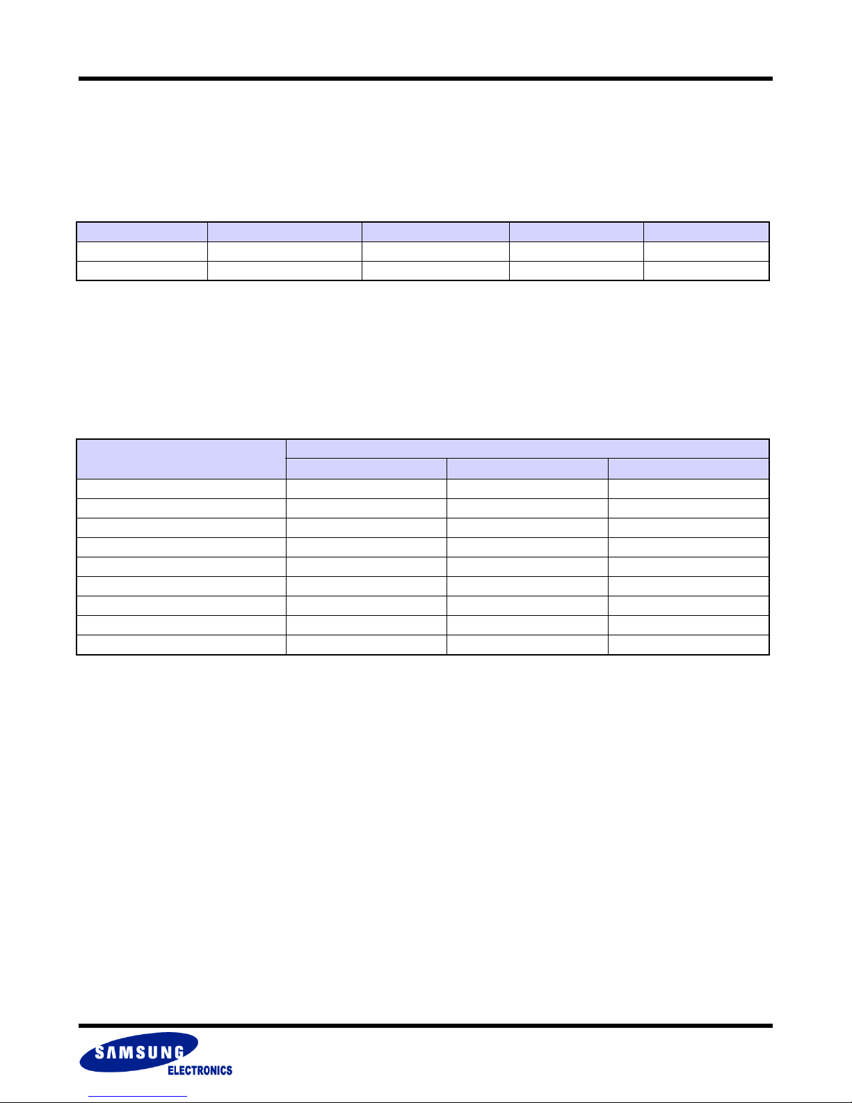
Density Part No. VCC(core & IO) Temperature PKG
2Gb KFM2G16Q2A-DEBx 1.8V(1.7V~1.95V) Extended 63FBGA(LF)
4Gb KFN4G16Q2A-DEBx 1.8V(1.7V~1.95V) Extended 63FBGA(LF)
1.1 Flash Product Type Selector
Samsung offers a variety of Flash solutions including NAND Flash, MuxOneNAND and NOR Flash. Samsung offers Flash products both
component and a variety of card formats including RS-MMC, MMC, CompactFlash, and SmartMedia.
To determine which Samsung Flash product solution is best for your application, refer the product selector chart.
Application Requires
Fast Random Read
Fast Sequential Read
Fast Write/Program
Multi Block Erase (Max 64 Blocks)
Erase Suspend/Resume
Copyback (EDC) (ECC)
Lock/Unlock/Lock-Tight
ECC External (Hardware/Software) Internal X
Scalability
NAND
Samsung Flash Products
MuxOneNAND
NOR
- 4 -
Page 5
MuxOneNAND2G(KFM2G16Q2A-DEBx)
MuxOneNAND4G(KFN4G16Q2A-DEBx)
1.2 Ordering Information
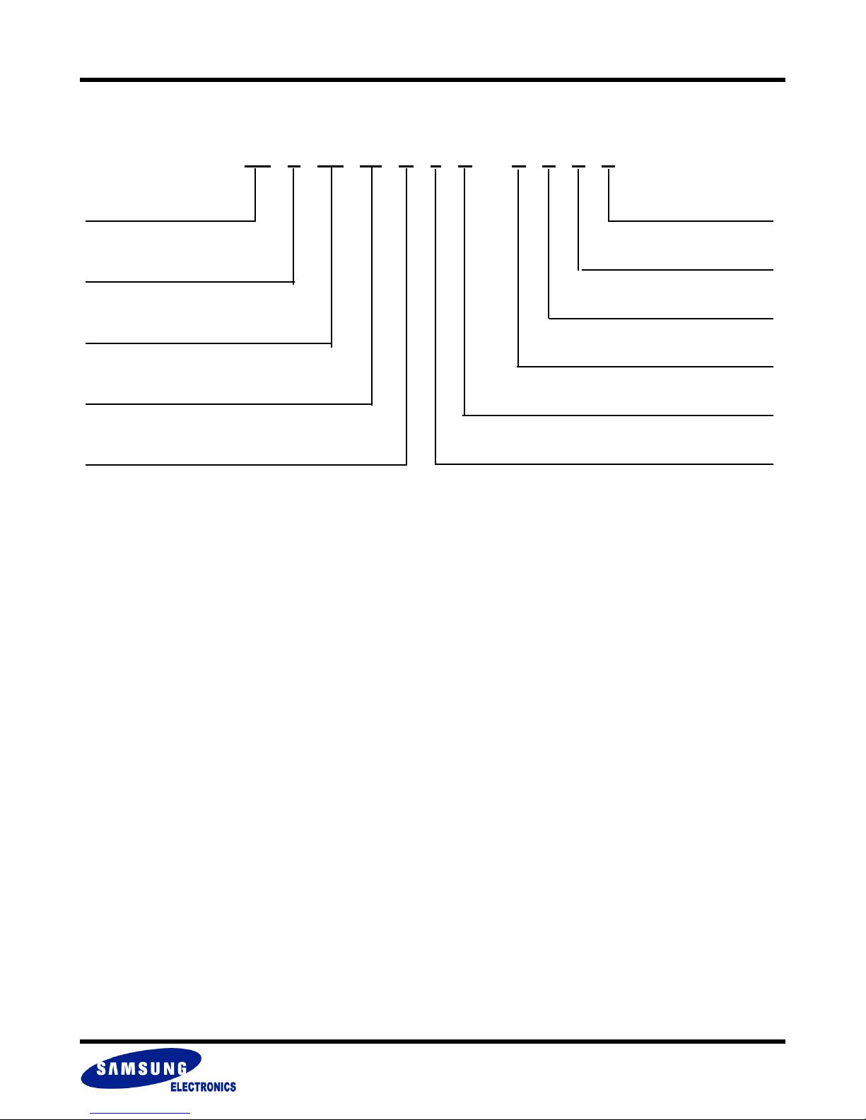
KF X XX 16 Q 2 A - D E X X
Samsung
MuxOneNAND Memory
Device Type
M : Single Chip
N : Dual Chip
Density
2G : 2Gb
4G : 4Gb
Organization
16 : x16 Organization
FLASH MEMORY
Speed
6 : 66MHz
8 : 83MHz
Product Line designator
B : Include Bad Block
D : Daisy Sample
Operating Temperature Range
E : Extended Temp. (-30 C to 85 C)
Package
D : FBGA(Lead Free)
Version
A : 2nd Generation
Operating Voltage Range
Q : 1.8V(1.7 V to 1.95V)
Page Architecture
2 : 2KB Page
1.3 Architectural Benefits
MuxOneNAND is a highly integrated non-volatile memory solution based around a NAND Flash memory array.
The chip integrates system features including:
A BootRAM and bootloader
Two independent bi-directional 2KB DataRAM buffers
A High-Speed x16 Host Interface
On-chip Error Correction
On-chip NOR interface controller
This on-chip integration enables system designers to reduce external system logic and use high-density NAND Flash in applications that
would otherwise have to use more NOR components.
MuxOneNAND takes advantage of the higher performance NAND program time, low power, and high density and combines it with the synchronous read performance of NOR. The NOR Flash host interface makes MuxOneNAND an ideal solution for applications like G3 Smart
Phones, Camera Phones, and mobile applications that have large, advanced multimedia applications and operating systems, but lack a
NAND controller.
When integrated into a Samsung Multi-Chip-Package with Samsung Mobile DDR SDRAM, designers can complete a high-performance,
small footprint solution.
- 5 -
Page 6
MuxOneNAND2G(KFM2G16Q2A-DEBx)
MuxOneNAND4G(KFN4G16Q2A-DEBx)
1.4 Product Features
Device Architecture
Design Technology:
Supply Voltage:
Host Interface:
5KB Internal BufferRAM:
SLC NAND Array:
Device Performance
Host Interface Type:
Programmable Burst Read Latency:
Multiple Sector Read/Write:
Multiple Reset Modes:
Multi Block Erase:
Low Power Dissipation:
Reliability
FLASH MEMORY
A die
1.8V (1.7V ~ 1.95V)
16 bit
1KB BootRAM, 4KB DataRAM
(2K+64)B Page Size, (128K+4K)B Block Size
Synchronous Burst Read
- Up to 83MHz clock frequency
- Linear Burst 4-, 8-, 16-, 32-words with wrap around
- Continuous 1K words Sequential Burst
Synchronous Burst Block Read
- Up to 83MHz clock frequency
- Linear Burst 4-, 8-, 16-, 32-, 1K-words with no-wrap
- Continuous (1K words) 64 Page Sequential Burst
Synchronous Write
- Up to 83MHz clock frequency
- Linear Burst 4-, 8-, 16-, 32-, 1K-words with wrap around
- Continuous 1K words Sequential Burst
Asynchronous Random Read
- 76ns access time
Asynchronous Random Write
Latency 3,4(Default),5,6 and 7.
1~40Mhz : Latency 3 available
1~66Mhz : Latency 4,5,6 and 7 available
Over 66Mhz : Latency 6,7 available.
Up to 4 sectors using Sector Count Register
Cold/Warm/Hot/NAND Flash Core Resets
up to 64 Blocks
Typic al P owe r,
- Standby current : 10uA (Single)
- Synchronous Burst Read current(66MHz/83MHz, single) : 20/25mA
- Synchronous Burst Write current(66MHz/83MHz, single) : 20/25mA
- Load current : 30mA
- Program current : 25mA
- Erase current : 20mA
- Multi Block Erase current : 20mA
- Data retention 10year after 10K Program/Erase Cycles
- Data retention 1year after 100K Program/Erase Cycles
System Hardware
Voltage detector generating internal reset signal from Vcc
Hardware reset input (RP
Data Protection Modes
User-controlled One Time Programmable(OTP) area
Internal 2bit EDC / 1bit ECC
Internal Bootloader supports Booting Solution in system
Handshaking Feature
Detailed chip information
Packaging
2G products
4G DDP products
)
- Write Protection for BootRAM
- Write Protection for NAND Flash Array
- Write Protection during power-up
- Write Protection during power-down
- INT pin indicates Ready / Busy
- Polling the interrupt register status bit
- by ID register
63ball, 10mm x 13mm x max 1.0mmt , 0.8mm ball pitch FBGA
63ball, 10mm x 13mm x max 1.2mmt , 0.8mm ball pitch FBGA
- 6 -
Page 7
MuxOneNAND2G(KFM2G16Q2A-DEBx)
MuxOneNAND4G(KFN4G16Q2A-DEBx)
1.5 General Overview
MuxOneNAND‚ is a monolithic integrated circuit with a NAND Flash array using a NOR Flash interface. This device includes control logic, a
NAND Flash array, and 5KB of internal BufferRAM. The BufferRAM reserves 1KB for boot code buffering (BootRAM) and 4KB for data buffering (DataRAM), split between 2 independent buffers. It has a x16 Host Interface and a random access time speed of ~76ns.
The device operates up to a maximum host-driven clock frequency of 66MHz / 83MHz for synchronous reads at Vcc(or Vccq. Refer to chapter
4.2) with minimum 4-clock (66MHz) / 6-clock (83MHz) latency. Below 40MHz it is accessible with minimum 3-clock latency. Appropriate wait
cycles are determined by programmable read latency.
MuxOneNAND provides for multiple sector read operations by assigning the number of sectors to be read in the sector counter
register. The device includes one block-sized OTP (One Time Programmable) area and user-controlled 1st block OTP(Block 0) that can be
used to increase system security or to provide identification capabilities.
FLASH MEMORY
The attached datasheets are prepared and approved by SAMSUNG Electronics. SAMSUNG Electronics CO., LTD. reserve the right to
change the specifications. SAMSUNG Electronics will evaluate and reply to your requests and questions about device. If you have any questions, please contact the SAMSUNG branch office near you.
- 7 -
Page 8
MuxOneNAND2G(KFM2G16Q2A-DEBx)
MuxOneNAND4G(KFN4G16Q2A-DEBx)
FLASH MEMORY
2.0 DEVICE DESCRIPTION
2.1 Detailed Product Description
The MuxOneNAND is an advanced generation, high-performance NAND-based Flash memory.
It integrates on-chip a single-level-cell (SLC) NAND Flash Array memory with two independent data buffers, boot RAM buffer, a page buffer for
the Flash array, and a one-time-programmable block.
The combination of these memory areas enable high-speed pipelining of reads from host
Clock speeds up to 66MHz / 83MHz with a x16 wide I/O yields a 108MByte/second bandwidth.
The MuxOneNAND also includes a Boot RAM and boot loader. This enables the device to efficiently load boot code at device startup from the
NAND Array without the need for off-chip boot device.
One block of the NAND Array is set aside as an OTP memory area, and 1st Block (Block 0) can be used as OTP area. This area, available to
the user, can be configured and locked with secured user information.
On-chip controller interfaces enable the device to operate in systems without NAND Host controllers.
BufferRAM Page Bufferand NAND Flash Array.
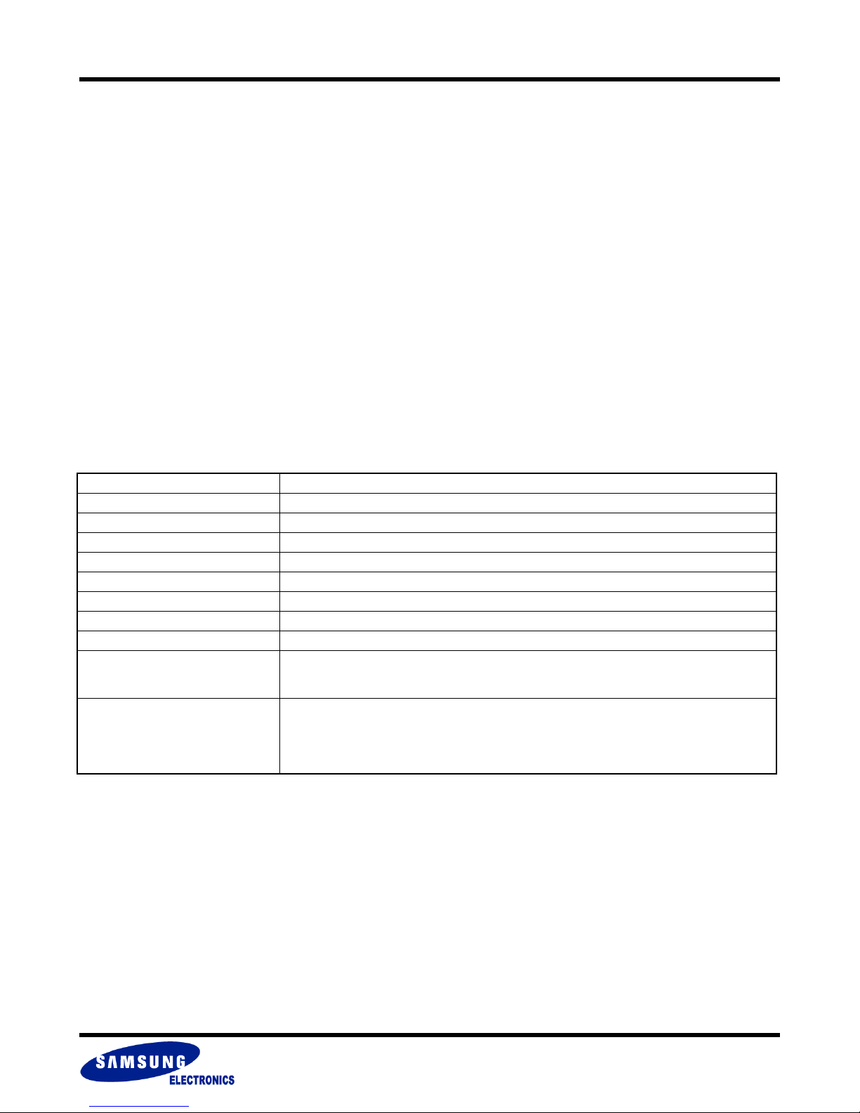
2.2 Definitions
B (capital letter) Byte, 8bits
W (capital letter) Word, 16bits
b (lower-case letter) Bit
ECC Error Correction Code
Calculated ECC ECC that has been calculated during a load or program access
Written ECC ECC that has been stored as data in the NAND Flash array or in the BufferRAM
BufferRAM On-chip internal buffer consisting of BootRAM and DataRAM
BootRAM A 1KB portion of the BufferRAM reserved for Boot Code buffering
DataRAM A 4KB portion of the BufferRAM reserved for Data buffering
Sector
Data unit
Part of a Page of which 512B is the main data area and 16B is the spare data area.
It is also the minimum Load/Program/Copy-Back Program unit
during a 1~4 sector operation is available.
Possible data unit to be read from memory to BufferRAM or to be programmed to memory.
- 528B of which 512B is in main area and 16B in spare area
- 1056B of which 1024B is in main area and 32B in spare area
- 1584B of which 1536B is in main area and 48B in spare area
- 2112B of which 2048B is in main area and 64B in spare area
- 8 -
Page 9
MuxOneNAND2G(KFM2G16Q2A-DEBx)
MuxOneNAND4G(KFN4G16Q2A-DEBx)
2.3 Pin Configuration
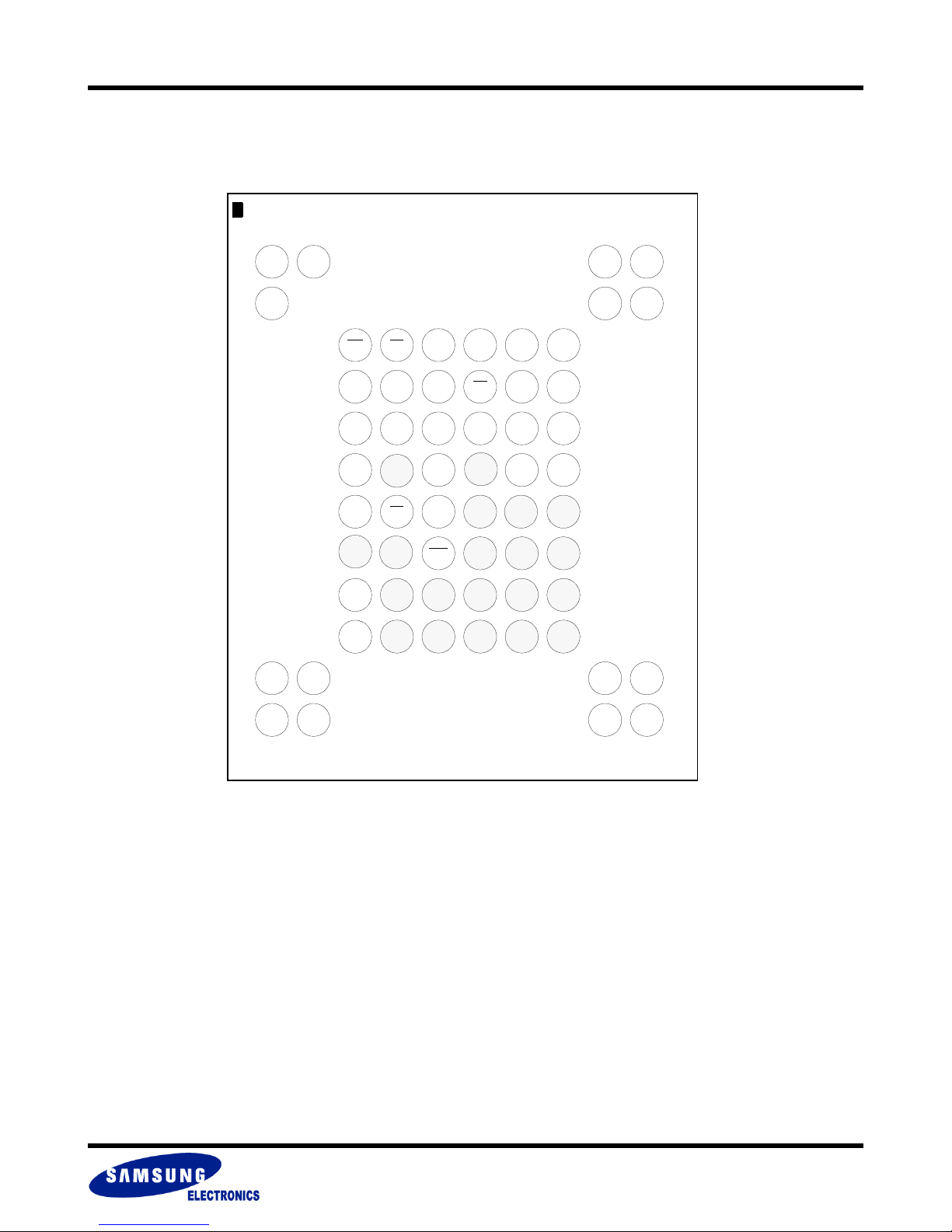
2.3.1 2Gb Product (KFM2G16Q2A)
NC NC NC NC
NC NC NC
FLASH MEMORY
WE RP ADQ1
ADQ3 ADQ7 ADQ14 OE ADQ6
ADQ8 ADQ11 ADQ4 ADQ5 ADQ12
ADQ0 NC ADQ15 ADQ10 ADQ9
CLK
CE ADQ13 NC NC NC
NC
NC
INT NC NC NC NC NC
NC NC NC NC NC
RDY
NC NC NC NC
NC NC NC NC
VSS VSS
NC
AVD NC NC NC
ADQ2
VCC
Core
VCC
IO
63ball, 10mm x 13mm x max 1.0mmt , 0.8mm ball pitch FBGA
(TOP VIEW, Balls Facing Down)
63ball FBGA MuxOneNAND Chip
- 9 -
Page 10
MuxOneNAND2G(KFM2G16Q2A-DEBx)
MuxOneNAND4G(KFN4G16Q2A-DEBx)
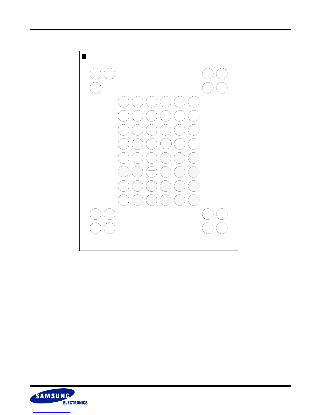
2.3.2 4Gb Product (KFN4G16Q2A)
NC NC NC NC
NC NC NC
FLASH MEMORY
WE RP ADQ1
ADQ3 ADQ7 ADQ14 OE ADQ6
ADQ8 ADQ11 ADQ4 ADQ5 ADQ12
ADQ0 NC ADQ15 ADQ10 ADQ9
CLK
CE ADQ13 NC NC NC
NC
NC
INT NC NC NC NC NC
NC NC NC NC NC
RDY
NC NC NC NC
NC NC NC NC
VSS VSS
NC
AVD NC NC NC
ADQ2
VCC
Core
VCC
IO
63ball, 10mm x 13mm x max 1.2mmt , 0.8mm ball pitch FBGA
(TOP VIEW, Balls Facing Down)
63ball FBGA MuxOneNAND Chip
- 10 -
Page 11
MuxOneNAND2G(KFM2G16Q2A-DEBx)
MuxOneNAND4G(KFN4G16Q2A-DEBx)
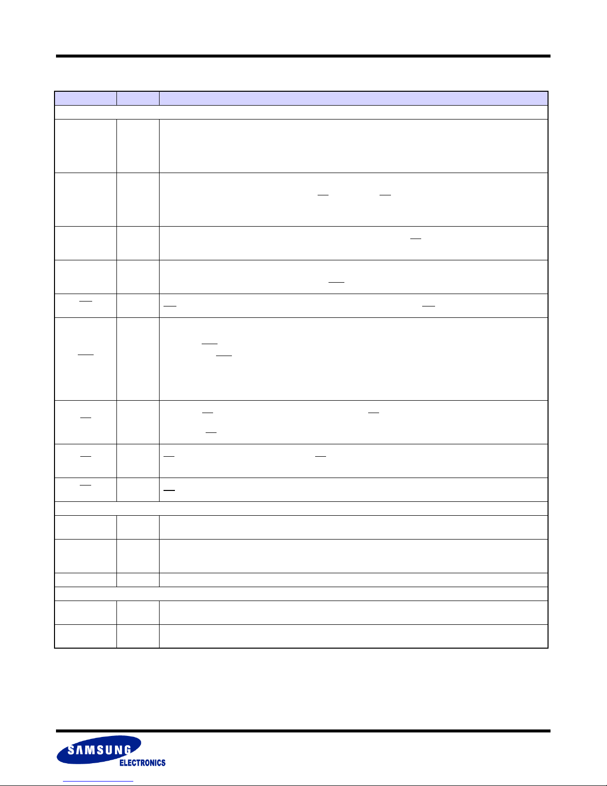
2.4 Pin Description
Pin Name Typ e Name and Description
Host Interface
Multiplexed Address/Data bus
- Inputs for addresses during read operation, which are for addressing BufferRAM & Register.
ADQ15~ADQ0 I/O
INT O
RDY O
CLK I
WE
AVD I
RP
CE
OE
Power Supply
CC-Core
V
/ Vcc
V
CC-IO
/ Vccq
V
SS Ground for MuxOneNAND
etc.
DNU
NC
NOTE :
Do not leave power supply(Vcc-Core/Vcc-IO, V
- Inputs data during program and commands for all operations, outputs data during memory array/
register read cycles.
Data pins float to high-impedance when the chip is deselected or outputs are disabled.
Interrupt
Notifies the Host when a command is completed. After power-up, it is at hi-z condition. Once IOBE is set to 1,
it does not float to hi-z condition even when CE
when reset(Warm, Hot, NAND Flash Core) command and ‘2X program’ command(007Dh) issued, it operates
as open drain output with internal resistor (~50Kohm).
Ready
Indicates data valid in synchronous read modes and is activated while CE
RDY pin may not be used in Non-Handshaking Mode. (Refer to Chapter 7.1)
Clock
CLK synchronizes the device to the system bus frequency in synchronous read mode.
The first rising edge of CLK in conjunction with AVD
Write Enable
I
WE
controls writes to the bufferRAM and registers. Data is latched on the WE pulse’s rising edge
Address Valid Detect
Indicates valid address presence on address inputs. During asynchronous read operation, all addresses are
latched on AVD
ing edge while AVD
> Low : for asynchronous mode, indicates valid address ;for burst mode,
> High : device ignores address inputs
Reset Pin
When low, RP
I
and bootloading.
When high, RP
Chip Enable
I
CE-low activates internal control logic, and CE-high deselects the device, places it in standby state,
and places A/DQ in Hi-Z
Output Enable
I
OE
-low enables the device’s output data buffers during a read cycle.
Power for MuxOneNAND Core
This is the power supply for MuxOneNAND Core.
Power for MuxOneNAND I/O
This is the power supply for MuxOneNAND I/O
Vcc-IO / Vccq is internally separated from Vcc-Core / Vcc.
Do Not Use
Leave it disconnected. These pins are used for testing.
No Connection
Lead is not internally connected.
’s rising edge, and during synchronous read operation, all addresses are latched on CLK’s ris-
is held low for one clock cycle.
causes starting address to be latched on rising edge on CLK
resets internal operation of MuxOneNAND. RP status is don’t care during power-up
level must be equivalent to Vcc-IO / Vccq level.
SS) disconnected.
is disabled or OE is disabled. Especially, in case of DDP,
low latches address input.
FLASH MEMORY
is low.
- 11 -
Page 12
MuxOneNAND2G(KFM2G16Q2A-DEBx)
MuxOneNAND4G(KFN4G16Q2A-DEBx)
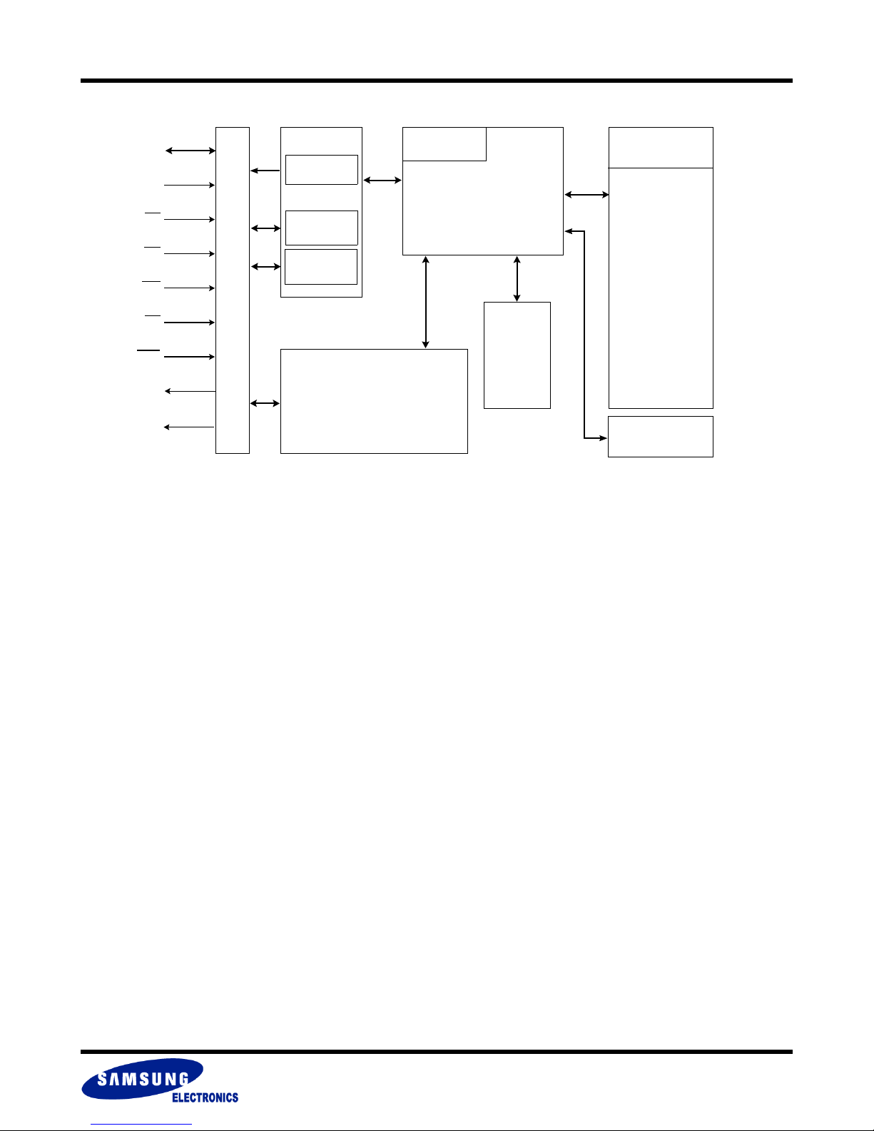
2.5 Block Diagram
FLASH MEMORY
ADQ15~ADQ0
CLK
CE
OE
WE
RP
AVD
INT
RDY
Host Interface
BufferRAM
BootRAM
DataRAM0
DataRAM1
(Address/Command/Configuration
2.6 Memory Array Organization
Internal Registers
/Status Registers)
Bootloader
StateMachine
1st Block OTP
(Block 0)
NAND Flash
Array
Error
Correction
Logic
OTP
(One Block)
The MuxOneNAND architecture integrates several memory areas on a single chip.
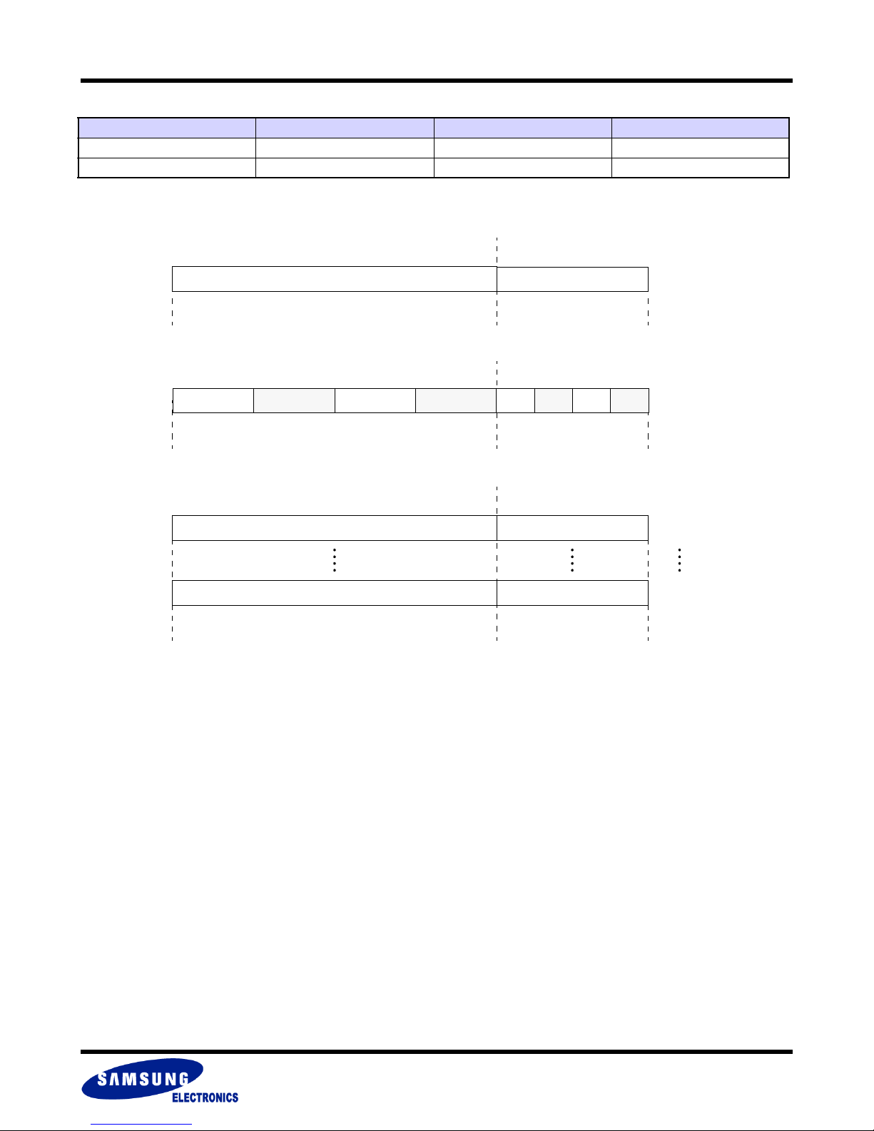
2.6.1 Internal (NAND Array) Memory Organization
The on-chip internal memory is a single-level-cell (SLC) NAND array used for data storage and code. The internal memory is divided into a
main area and a spare area.
Main Area
The main area is the primary memory array. This main area is divided into Blocks of 64 Pages. Within a Block, each Page is 2KB and is comprised of 4 Sectors. Within a Page, each Sector is 512B and is comprised of 256 Words.
Spare Area
The spare area is used for invalid block information and ECC storage. Spare area internal memory is associated with corresponding main area
memory. Within a Block, each Page has four 16B Sectors of spare area. Each spare area Sector is 8 words.
- 12 -
Page 13
MuxOneNAND2G(KFM2G16Q2A-DEBx)
MuxOneNAND4G(KFN4G16Q2A-DEBx)
Internal Memory Array Information
Area Block Page Sector
Main 128KB 2KB 512B
Spare 4KB 64B 16B
Internal Memory Array Organization
Sector
Page
512B Sector0
Main Area Spare Area
Main Area Spare Area
512B Sector1
512B 16B
512B Sector2
2KB 64B
512B Sector3
16B Sector0 16B Sector1
16B Sector2
FLASH MEMORY
16B Sector3
Block
Main Area Spare Area
2KB Page0
2KB Page63 64B Page63
128KB 4KB
64B Page0
Page 0
Page 63
- 13 -
Page 14
MuxOneNAND2G(KFM2G16Q2A-DEBx)
MuxOneNAND4G(KFN4G16Q2A-DEBx)
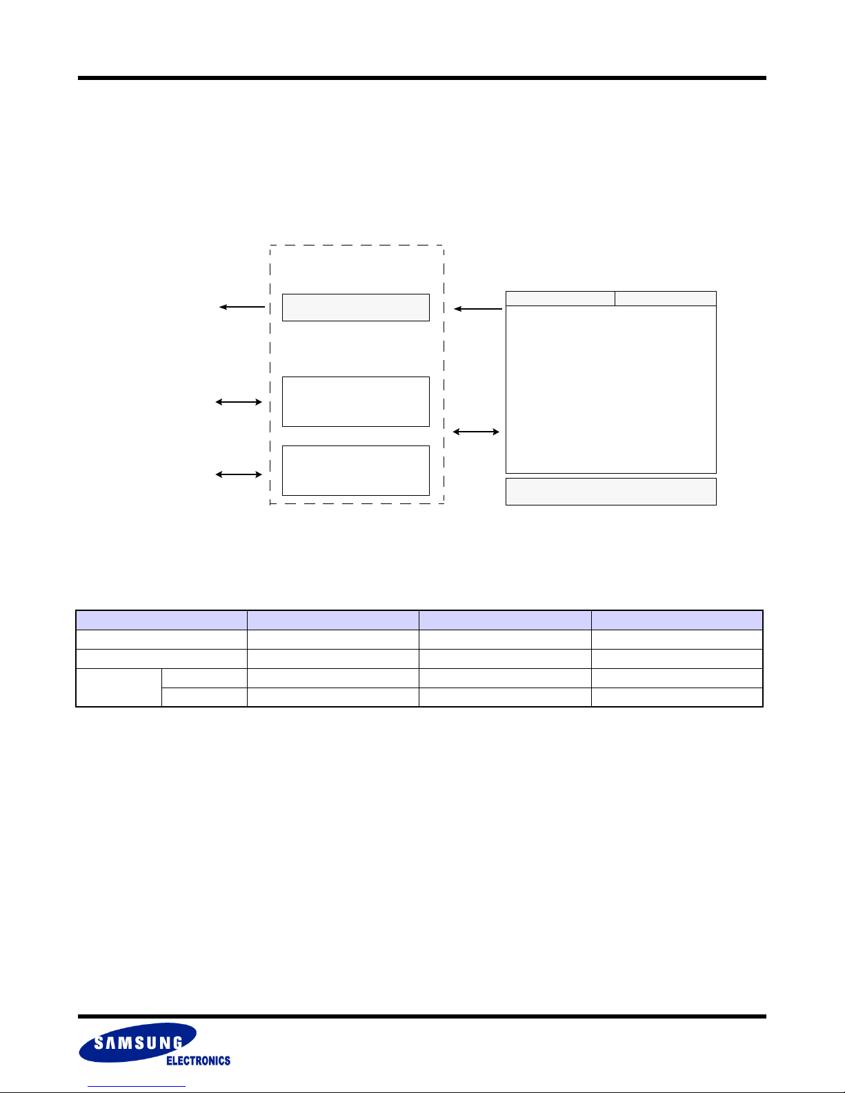
2.6.2 External (BufferRAM) Memory Organization
The on-chip external memory is comprised of 3 buffers used for Boot Code storage and data buffering.
The BootRAM is a 1KB buffer that receives Boot Code from the internal memory and makes it available to the host at start up.
There are two independent 2KB bi-directional data buffers, DataRAM0 and DataRAM1. These dual buffers enable the host to execute simultaneous Read-While load, and Write-While-program operations after Boot Up. During Boot Up, the BootRam is used by the host to initialize
the main memory, and deliver boot code from NAND Flash core to host.
FLASH MEMORY
External (BufferRAM)
Memory
BootRAM (1KB)
Host
DataRAM0 (2KB)
DataRAM1 (2KB)
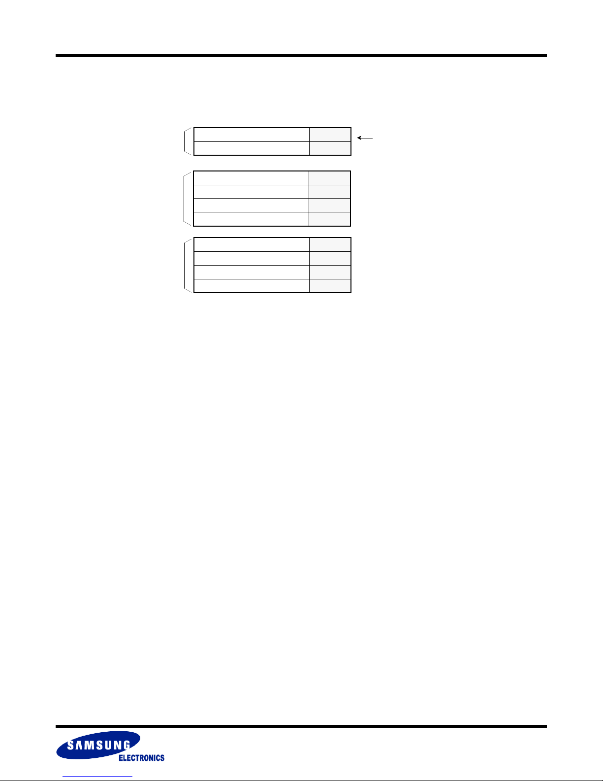
The external memory is divided into a main area and a spare area. Each buffer is the equivalent size of a Sector.
The main area data is 512B. The spare area data is 16B.
External Memory Array Information
Area BootRAM DataRAM0 DataRAM1
Total Size 1KB+32B 2KB+64B 2KB+64B
Number of Sectors 2 4 4
Sector
Main 512B 512B 512B
Spare 16B 16B 16B
Internal (Nand Array)
Memory
Boot code (1KB)
Nand Array
OTP Block
- 14 -
Page 15
MuxOneNAND2G(KFM2G16Q2A-DEBx)
MuxOneNAND4G(KFN4G16Q2A-DEBx)
External Memory Array Organization
FLASH MEMORY
BootRAM
DataRAM0
DataRAM1
Main area data
(512B)
BootRAM 0
BootRAM 1
DataRAM 0_0
DataRAM 0_1
DataRAM 0_2
DataRAM 0_3
DataRAM 1_0
DataRAM 1_1
DataRAM 1_2
DataRAM 1_3
Spare area data
(16B)
Sector: (512 + 16) Byte
- 15 -
Page 16
MuxOneNAND2G(KFM2G16Q2A-DEBx)
MuxOneNAND4G(KFN4G16Q2A-DEBx)
2.7 Memory Map
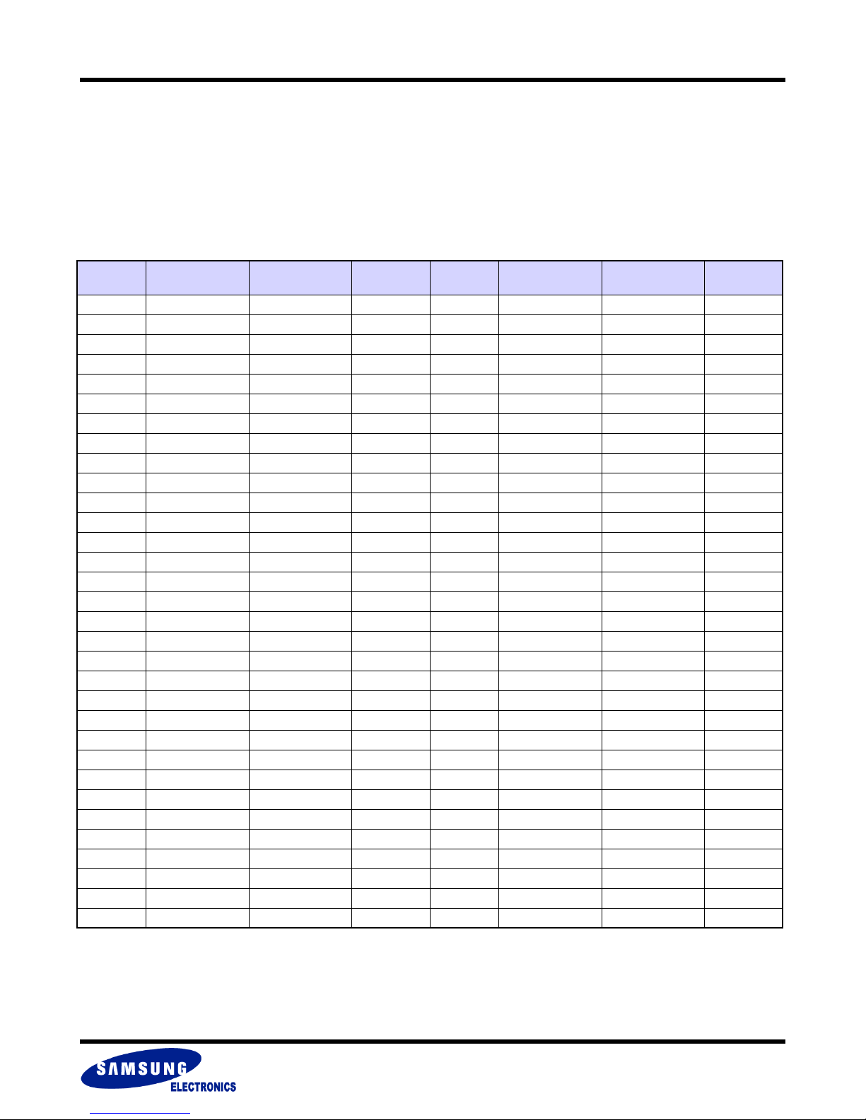
The following tables are the memory maps for the MuxOneNAND.
2.7.1 Internal (NAND Array) Memory Organization
The following tables show the Internal Memory address map in word order.
FLASH MEMORY
Block Block Address
Block0 0000h 0000h~00FFh 128KB Block32 0020h 0000h~00FFh 128KB
Block1 0001h 0000h~00FFh 128KB Block33 0021h 0000h~00FFh 128KB
Block2 0002h 0000h~00FFh 128KB Block34 0022h 0000h~00FFh 128KB
Block3 0003h 0000h~00FFh 128KB Block35 0023h 0000h~00FFh 128KB
Block4 0004h 0000h~00FFh 128KB Block36 0024h 0000h~00FFh 128KB
Block5 0005h 0000h~00FFh 128KB Block37 0025h 0000h~00FFh 128KB
Block6 0006h 0000h~00FFh 128KB Block38 0026h 0000h~00FFh 128KB
Block7 0007h 0000h~00FFh 128KB Block39 0027h 0000h~00FFh 128KB
Block8 0008h 0000h~00FFh 128KB Block40 0028h 0000h~00FFh 128KB
Block9 0009h 0000h~00FFh 128KB Block41 0029h 0000h~00FFh 128KB
Block10 000Ah 0000h~00FFh 128KB Block42 002Ah 0000h~00FFh 128KB
Block11 000Bh 0000h~00FFh 128KB Block43 002Bh 0000h~00FFh 128KB
Block12 000Ch 0000h~00FFh 128KB Block44 002Ch 0000h~00FFh 128KB
Block13 000Dh 0000h~00FFh 128KB Block45 002Dh 0000h~00FFh 128KB
Block14 000Eh 0000h~00FFh 128KB Block46 002Eh 0000h~00FFh 128KB
Block15 000Fh 0000h~00FFh 128KB Block47 002Fh 0000h~00FFh 128KB
Block16 0010h 0000h~00FFh 128KB Block48 0030h 0000h~00FFh 128KB
Block17 0011h 0000h~00FFh 128KB Block49 0031h 0000h~00FFh 128KB
Block18 0012h 0000h~00FFh 128KB Block50 0032h 0000h~00FFh 128KB
Block19 0013h 0000h~00FFh 128KB Block51 0033h 0000h~00FFh 128KB
Block20 0014h 0000h~00FFh 128KB Block52 0034h 0000h~00FFh 128KB
Block21 0015h 0000h~00FFh 128KB Block53 0035h 0000h~00FFh 128KB
Block22 0016h 0000h~00FFh 128KB Block54 0036h 0000h~00FFh 128KB
Block23 0017h 0000h~00FFh 128KB Block55 0037h 0000h~00FFh 128KB
Block24 0018h 0000h~00FFh 128KB Block56 0038h 0000h~00FFh 128KB
Block25 0019h 0000h~00FFh 128KB Block57 0039h 0000h~00FFh 128KB
Block26 001Ah 0000h~00FFh 128KB Block58 003Ah 0000h~00FFh 128KB
Block27 001Bh 0000h~00FFh 128KB Block59 003Bh 0000h~00FFh 128KB
Block28 001Ch 0000h~00FFh 128KB Block60 003Ch 0000h~00FFh 128KB
Block29 001Dh 0000h~00FFh 128KB Block61 003Dh 0000h~00FFh 128KB
Block30 001Eh 0000h~00FFh 128KB Block62 003Eh 0000h~00FFh 128KB
Block31 001Fh 0000h~00FFh 128KB Block63 003Fh 0000h~00FFh 128KB
Page and Sector
Address
Size Block Block Address
Page and Sector
Address
Size
- 16 -
Page 17
MuxOneNAND2G(KFM2G16Q2A-DEBx)
MuxOneNAND4G(KFN4G16Q2A-DEBx)
FLASH MEMORY
Block Block Address
Block64 0040h 0000h~00FFh 128KB Block96 0060h 0000h~00FFh 128KB
Block65 0041h 0000h~00FFh 128KB Block97 0061h 0000h~00FFh 128KB
Block66 0042h 0000h~00FFh 128KB Block98 0062h 0000h~00FFh 128KB
Block67 0043h 0000h~00FFh 128KB Block99 0063h 0000h~00FFh 128KB
Block68 0044h 0000h~00FFh 128KB Block100 0064h 0000h~00FFh 128KB
Block69 0045h 0000h~00FFh 128KB Block101 0065h 0000h~00FFh 128KB
Block70 0046h 0000h~00FFh 128KB Block102 0066h 0000h~00FFh 128KB
Block71 0047h 0000h~00FFh 128KB Block103 0067h 0000h~00FFh 128KB
Block72 0048h 0000h~00FFh 128KB Block104 0068h 0000h~00FFh 128KB
Block73 0049h 0000h~00FFh 128KB Block105 0069h 0000h~00FFh 128KB
Block74 004Ah 0000h~00FFh 128KB Block106 006Ah 0000h~00FFh 128KB
Block75 004Bh 0000h~00FFh 128KB Block107 006Bh 0000h~00FFh 128KB
Block76 004Ch 0000h~00FFh 128KB Block108 006Ch 0000h~00FFh 128KB
Block77 004Dh 0000h~00FFh 128KB Block109 006Dh 0000h~00FFh 128KB
Block78 004Eh 0000h~00FFh 128KB Block110 006Eh 0000h~00FFh 128KB
Block79 004Fh 0000h~00FFh 128KB Block111 006Fh 0000h~00FFh 128KB
Block80 0050h 0000h~00FFh 128KB Block112 0070h 0000h~00FFh 128KB
Block81 0051h 0000h~00FFh 128KB Block113 0071h 0000h~00FFh 128KB
Block82 0052h 0000h~00FFh 128KB Block114 0072h 0000h~00FFh 128KB
Block83 0053h 0000h~00FFh 128KB Block115 0073h 0000h~00FFh 128KB
Block84 0054h 0000h~00FFh 128KB Block116 0074h 0000h~00FFh 128KB
Block85 0055h 0000h~00FFh 128KB Block117 0075h 0000h~00FFh 128KB
Block86 0056h 0000h~00FFh 128KB Block118 0076h 0000h~00FFh 128KB
Block87 0057h 0000h~00FFh 128KB Block119 0077h 0000h~00FFh 128KB
Block88 0058h 0000h~00FFh 128KB Block120 0078h 0000h~00FFh 128KB
Block89 0059h 0000h~00FFh 128KB Block121 0079h 0000h~00FFh 128KB
Block90 005Ah 0000h~00FFh 128KB Block122 007Ah 0000h~00FFh 128KB
Block91 005Bh 0000h~00FFh 128KB Block123 007Bh 0000h~00FFh 128KB
Block92 005Ch 0000h~00FFh 128KB Block124 007Ch 0000h~00FFh 128KB
Block93 005Dh 0000h~00FFh 128KB Block125 007Dh 0000h~00FFh 128KB
Block94 005Eh 0000h~00FFh 128KB Block126 007Eh 0000h~00FFh 128KB
Block95 005Fh 0000h~00FFh 128KB Block127 007Fh 0000h~00FFh 128KB
Page and Sector
Address
Size Block Block Address
Page and Sector
Address
Size
- 17 -
Page 18

MuxOneNAND2G(KFM2G16Q2A-DEBx)
MuxOneNAND4G(KFN4G16Q2A-DEBx)
FLASH MEMORY
Block Block Address
Block128 0080h 0000h~00FFh 128KB Block160 00A0h 0000h~00FFh 128KB
Block129 0081h 0000h~00FFh 128KB Block161 00A1h 0000h~00FFh 128KB
Block130 0082h 0000h~00FFh 128KB Block162 00A2h 0000h~00FFh 128KB
Block131 0083h 0000h~00FFh 128KB Block163 00A3h 0000h~00FFh 128KB
Block132 0084h 0000h~00FFh 128KB Block164 00A4h 0000h~00FFh 128KB
Block133 0085h 0000h~00FFh 128KB Block165 00A5h 0000h~00FFh 128KB
Block134 0086h 0000h~00FFh 128KB Block166 00A6h 0000h~00FFh 128KB
Block135 0087h 0000h~00FFh 128KB Block167 00A7h 0000h~00FFh 128KB
Block136 0088h 0000h~00FFh 128KB Block168 00A8h 0000h~00FFh 128KB
Block137 0089h 0000h~00FFh 128KB Block169 00A9h 0000h~00FFh 128KB
Block138 008Ah 0000h~00FFh 128KB Block170 00AAh 0000h~00FFh 128KB
Block139 008Bh 0000h~00FFh 128KB Block171 00ABh 0000h~00FFh 128KB
Block140 008Ch 0000h~00FFh 128KB Block172 00ACh 0000h~00FFh 128KB
Block141 008Dh 0000h~00FFh 128KB Block173 00ADh 0000h~00FFh 128KB
Block142 008Eh 0000h~00FFh 128KB Block174 00AEh 0000h~00FFh 128KB
Block143 008Fh 0000h~00FFh 128KB Block175 00AFh 0000h~00FFh 128KB
Block144 0090h 0000h~00FFh 128KB Block176 00B0h 0000h~00FFh 128KB
Block145 0091h 0000h~00FFh 128KB Block177 00B1h 0000h~00FFh 128KB
Block146 0092h 0000h~00FFh 128KB Block178 00B2h 0000h~00FFh 128KB
Block147 0093h 0000h~00FFh 128KB Block179 00B3h 0000h~00FFh 128KB
Block148 0094h 0000h~00FFh 128KB Block180 00B4h 0000h~00FFh 128KB
Block149 0095h 0000h~00FFh 128KB Block181 00B5h 0000h~00FFh 128KB
Block150 0096h 0000h~00FFh 128KB Block182 00B6h 0000h~00FFh 128KB
Block151 0097h 0000h~00FFh 128KB Block183 00B7h 0000h~00FFh 128KB
Block152 0098h 0000h~00FFh 128KB Block184 00B8h 0000h~00FFh 128KB
Block153 0099h 0000h~00FFh 128KB Block185 00B9h 0000h~00FFh 128KB
Block154 009Ah 0000h~00FFh 128KB Block186 00BAh 0000h~00FFh 128KB
Block155 009Bh 0000h~00FFh 128KB Block187 00BBh 0000h~00FFh 128KB
Block156 009Ch 0000h~00FFh 128KB Block188 00BCh 0000h~00FFh 128KB
Block157 009Dh 0000h~00FFh 128KB Block189 00BDh 0000h~00FFh 128KB
Block158 009Eh 0000h~00FFh 128KB Block190 00BEh 0000h~00FFh 128KB
Block159 009Fh 0000h~00FFh 128KB Block191 00BFh 0000h~00FFh 128KB
Page and Sector
Address
Size Block Block Address
Page and Sector
Address
Size
- 18 -
Page 19
MuxOneNAND2G(KFM2G16Q2A-DEBx)
MuxOneNAND4G(KFN4G16Q2A-DEBx)
FLASH MEMORY
Block Block Address
Block192 00C0h 0000h~00FFh 128KB Block224 00E0h 0000h~00FFh 128KB
Block193 00C1h 0000h~00FFh 128KB Block225 00E1h 0000h~00FFh 128KB
Block194 00C2h 0000h~00FFh 128KB Block226 00E2h 0000h~00FFh 128KB
Block195 00C3h 0000h~00FFh 128KB Block227 00E3h 0000h~00FFh 128KB
Block196 00C4h 0000h~00FFh 128KB Block228 00E4h 0000h~00FFh 128KB
Block197 00C5h 0000h~00FFh 128KB Block229 00E5h 0000h~00FFh 128KB
Block198 00C6h 0000h~00FFh 128KB Block230 00E6h 0000h~00FFh 128KB
Block199 00C7h 0000h~00FFh 128KB Block231 00E7h 0000h~00FFh 128KB
Block200 00C8h 0000h~00FFh 128KB Block232 00E8h 0000h~00FFh 128KB
Block201 00C9h 0000h~00FFh 128KB Block233 00E9h 0000h~00FFh 128KB
Block202 00CAh 0000h~00FFh 128KB Block234 00EAh 0000h~00FFh 128KB
Block203 00CBh 0000h~00FFh 128KB Block235 00EBh 0000h~00FFh 128KB
Block204 00CCh 0000h~00FFh 128KB Block236 00ECh 0000h~00FFh 128KB
Block205 00CDh 0000h~00FFh 128KB Block237 00EDh 0000h~00FFh 128KB
Block206 00CEh 0000h~00FFh 128KB Block238 00EEh 0000h~00FFh 128KB
Block207 00CFh 0000h~00FFh 128KB Block239 00EFh 0000h~00FFh 128KB
Block208 00D0h 0000h~00FFh 128KB Block240 00F0h 0000h~00FFh 128KB
Block209 00D1h 0000h~00FFh 128KB Block241 00F1h 0000h~00FFh 128KB
Block210 00D2h 0000h~00FFh 128KB Block242 00F2h 0000h~00FFh 128KB
Block211 00D3h 0000h~00FFh 128KB Block243 00F3h 0000h~00FFh 128KB
Block212 00D4h 0000h~00FFh 128KB Block244 00F4h 0000h~00FFh 128KB
Block213 00D5h 0000h~00FFh 128KB Block245 00F5h 0000h~00FFh 128KB
Block214 00D6h 0000h~00FFh 128KB Block246 00F6h 0000h~00FFh 128KB
Block215 00D7h 0000h~00FFh 128KB Block247 00F7h 0000h~00FFh 128KB
Block216 00D8h 0000h~00FFh 128KB Block248 00F8h 0000h~00FFh 128KB
Block217 00D9h 0000h~00FFh 128KB Block249 00F9h 0000h~00FFh 128KB
Block218 00DAh 0000h~00FFh 128KB Block250 00FAh 0000h~00FFh 128KB
Block219 00DBh 0000h~00FFh 128KB Block251 00FBh 0000h~00FFh 128KB
Block220 00DCh 0000h~00FFh 128KB Block252 00FCh 0000h~00FFh 128KB
Block221 00DDh 0000h~00FFh 128KB Block253 00FDh 0000h~00FFh 128KB
Block222 00DEh 0000h~00FFh 128KB Block254 00FEh 0000h~00FFh 128KB
Block223 00DFh 0000h~00FFh 128KB Block255 00FFh 0000h~00FFh 128KB
Page and Sector
Address
Size Block Block Address
Page and Sector
Address
Size
- 19 -
Page 20
MuxOneNAND2G(KFM2G16Q2A-DEBx)
MuxOneNAND4G(KFN4G16Q2A-DEBx)
FLASH MEMORY
Block Block Address
Block256 0100h 0000h~00FFh 128KB Block288 0120h 0000h~00FFh 128KB
Block257 0101h 0000h~00FFh 128KB Block289 0121h 0000h~00FFh 128KB
Block258 0102h 0000h~00FFh 128KB Block290 0122h 0000h~00FFh 128KB
Block259 0103h 0000h~00FFh 128KB Block291 0123h 0000h~00FFh 128KB
Block260 0104h 0000h~00FFh 128KB Block292 0124h 0000h~00FFh 128KB
Block261 0105h 0000h~00FFh 128KB Block293 0125h 0000h~00FFh 128KB
Block262 0106h 0000h~00FFh 128KB Block294 0126h 0000h~00FFh 128KB
Block263 0107h 0000h~00FFh 128KB Block295 0127h 0000h~00FFh 128KB
Block264 0108h 0000h~00FFh 128KB Block296 0128h 0000h~00FFh 128KB
Block265 0109h 0000h~00FFh 128KB Block297 0129h 0000h~00FFh 128KB
Block266 010Ah 0000h~00FFh 128KB Block298 012Ah 0000h~00FFh 128KB
Block267 010Bh 0000h~00FFh 128KB Block299 012Bh 0000h~00FFh 128KB
Block268 010Ch 0000h~00FFh 128KB Block300 012Ch 0000h~00FFh 128KB
Block269 010Dh 0000h~00FFh 128KB Block301 012Dh 0000h~00FFh 128KB
Block270 010Eh 0000h~00FFh 128KB Block302 012Eh 0000h~00FFh 128KB
Block271 010Fh 0000h~00FFh 128KB Block303 012Fh 0000h~00FFh 128KB
Block272 0110h 0000h~00FFh 128KB Block304 0130h 0000h~00FFh 128KB
Block273 0111h 0000h~00FFh 128KB Block305 0131h 0000h~00FFh 128KB
Block274 0112h 0000h~00FFh 128KB Block306 0132h 0000h~00FFh 128KB
Block275 0113h 0000h~00FFh 128KB Block307 0133h 0000h~00FFh 128KB
Block276 0114h 0000h~00FFh 128KB Block308 0134h 0000h~00FFh 128KB
Block277 0115h 0000h~00FFh 128KB Block309 0135h 0000h~00FFh 128KB
Block278 0116h 0000h~00FFh 128KB Block310 0136h 0000h~00FFh 128KB
Block279 0117h 0000h~00FFh 128KB Block311 0137h 0000h~00FFh 128KB
Block280 0118h 0000h~00FFh 128KB Block312 0138h 0000h~00FFh 128KB
Block281 0119h 0000h~00FFh 128KB Block313 0139h 0000h~00FFh 128KB
Block282 011Ah 0000h~00FFh 128KB Block314 013Ah 0000h~00FFh 128KB
Block283 011Bh 0000h~00FFh 128KB Block315 013Bh 0000h~00FFh 128KB
Block284 011Ch 0000h~00FFh 128KB Block316 013Ch 0000h~00FFh 128KB
Block285 011Dh 0000h~00FFh 128KB Block317 013Dh 0000h~00FFh 128KB
Block286 011Eh 0000h~00FFh 128KB Block318 013Eh 0000h~00FFh 128KB
Block287 011Fh 0000h~00FFh 128KB Block319 013Fh 0000h~00FFh 128KB
Page and Sector
Address
Size Block Block Address
Page and Sector
Address
Size
- 20 -
Page 21
MuxOneNAND2G(KFM2G16Q2A-DEBx)
MuxOneNAND4G(KFN4G16Q2A-DEBx)
FLASH MEMORY
Block Block Address
Block320 0140h 0000h~00FFh 128KB Block352 0160h 0000h~00FFh 128KB
Block321 0141h 0000h~00FFh 128KB Block353 0161h 0000h~00FFh 128KB
Block322 0142h 0000h~00FFh 128KB Block354 0162h 0000h~00FFh 128KB
Block323 0143h 0000h~00FFh 128KB Block355 0163h 0000h~00FFh 128KB
Block324 0144h 0000h~00FFh 128KB Block356 0164h 0000h~00FFh 128KB
Block325 0145h 0000h~00FFh 128KB Block357 0165h 0000h~00FFh 128KB
Block326 0146h 0000h~00FFh 128KB Block358 0166h 0000h~00FFh 128KB
Block327 0147h 0000h~00FFh 128KB Block359 0167h 0000h~00FFh 128KB
Block328 0148h 0000h~00FFh 128KB Block360 0168h 0000h~00FFh 128KB
Block329 0149h 0000h~00FFh 128KB Block361 0169h 0000h~00FFh 128KB
Block330 014Ah 0000h~00FFh 128KB Block362 016Ah 0000h~00FFh 128KB
Block331 014Bh 0000h~00FFh 128KB Block363 016Bh 0000h~00FFh 128KB
Block332 014Ch 0000h~00FFh 128KB Block364 016Ch 0000h~00FFh 128KB
Block333 014Dh 0000h~00FFh 128KB Block365 016Dh 0000h~00FFh 128KB
Block334 014Eh 0000h~00FFh 128KB Block366 016Eh 0000h~00FFh 128KB
Block335 014Fh 0000h~00FFh 128KB Block367 016Fh 0000h~00FFh 128KB
Block336 0150h 0000h~00FFh 128KB Block368 0170h 0000h~00FFh 128KB
Block337 0151h 0000h~00FFh 128KB Block369 0171h 0000h~00FFh 128KB
Block338 0152h 0000h~00FFh 128KB Block370 0172h 0000h~00FFh 128KB
Block339 0153h 0000h~00FFh 128KB Block371 0173h 0000h~00FFh 128KB
Block340 0154h 0000h~00FFh 128KB Block372 0174h 0000h~00FFh 128KB
Block341 0155h 0000h~00FFh 128KB Block373 0175h 0000h~00FFh 128KB
Block342 0156h 0000h~00FFh 128KB Block374 0176h 0000h~00FFh 128KB
Block343 0157h 0000h~00FFh 128KB Block375 0177h 0000h~00FFh 128KB
Block344 0158h 0000h~00FFh 128KB Block376 0178h 0000h~00FFh 128KB
Block345 0159h 0000h~00FFh 128KB Block377 0179h 0000h~00FFh 128KB
Block346 015Ah 0000h~00FFh 128KB Block378 017Ah 0000h~00FFh 128KB
Block347 015Bh 0000h~00FFh 128KB Block379 017Bh 0000h~00FFh 128KB
Block348 015Ch 0000h~00FFh 128KB Block380 017Ch 0000h~00FFh 128KB
Block349 015Dh 0000h~00FFh 128KB Block381 017Dh 0000h~00FFh 128KB
Block350 015Eh 0000h~00FFh 128KB Block382 017Eh 0000h~00FFh 128KB
Block351 015Fh 0000h~00FFh 128KB Block383 017Fh 0000h~00FFh 128KB
Page and Sector
Address
Size Block Block Address
Page and Sector
Address
Size
- 21 -
Page 22
MuxOneNAND2G(KFM2G16Q2A-DEBx)
MuxOneNAND4G(KFN4G16Q2A-DEBx)
FLASH MEMORY
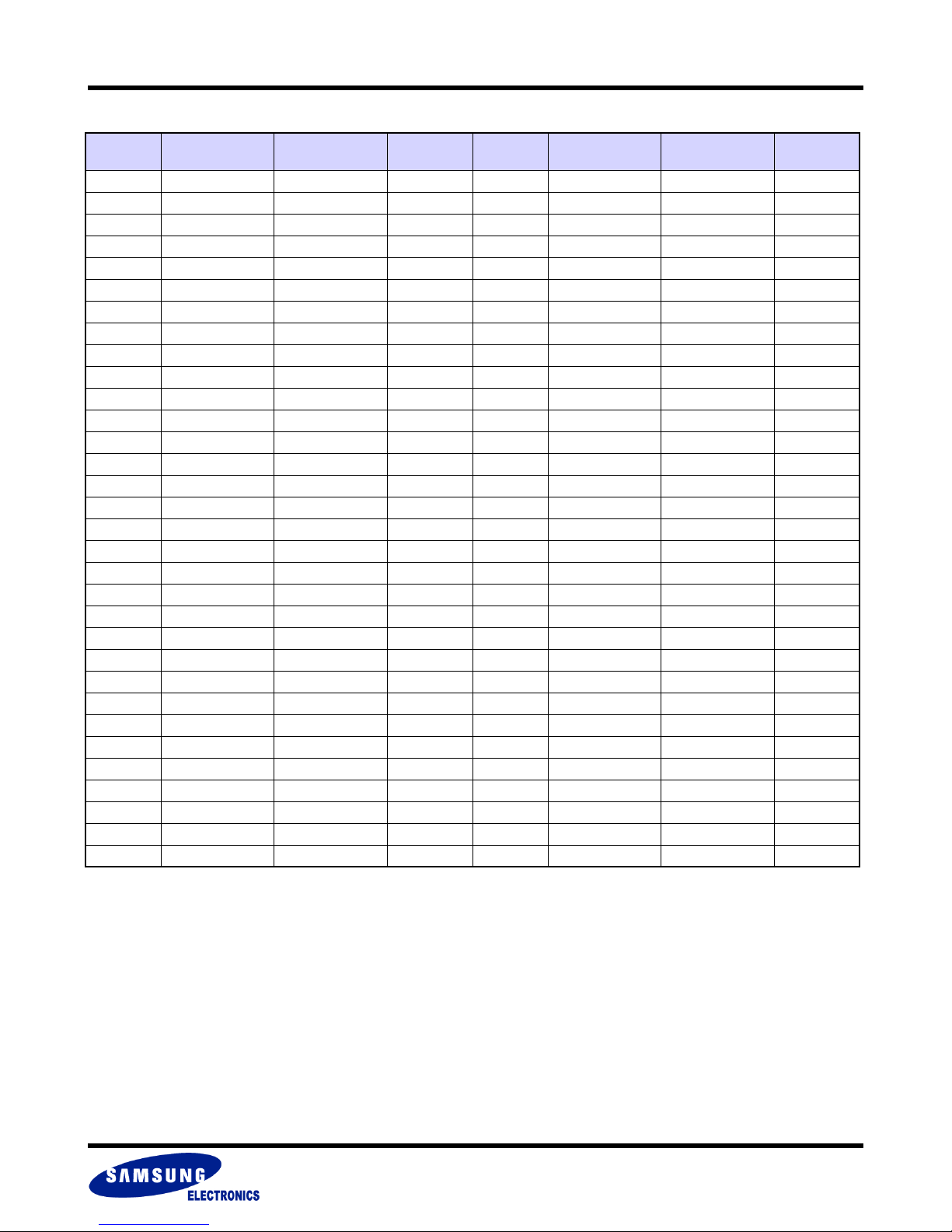
Block Block Address
Block384 0180h 0000h~00FFh 128KB Block416 01A0h 0000h~00FFh 128KB
Block385 0181h 0000h~00FFh 128KB Block417 01A1h 0000h~00FFh 128KB
Block386 0182h 0000h~00FFh 128KB Block418 01A2h 0000h~00FFh 128KB
Block387 0183h 0000h~00FFh 128KB Block419 01A3h 0000h~00FFh 128KB
Block388 0184h 0000h~00FFh 128KB Block420 01A4h 0000h~00FFh 128KB
Block389 0185h 0000h~00FFh 128KB Block421 01A5h 0000h~00FFh 128KB
Block390 0186h 0000h~00FFh 128KB Block422 01A6h 0000h~00FFh 128KB
Block391 0187h 0000h~00FFh 128KB Block423 01A7h 0000h~00FFh 128KB
Block392 0188h 0000h~00FFh 128KB Block424 01A8h 0000h~00FFh 128KB
Block393 0189h 0000h~00FFh 128KB Block425 01A9h 0000h~00FFh 128KB
Block394 018Ah 0000h~00FFh 128KB Block426 01AAh 0000h~00FFh 128KB
Block395 018Bh 0000h~00FFh 128KB Block427 01ABh 0000h~00FFh 128KB
Block396 018Ch 0000h~00FFh 128KB Block428 01ACh 0000h~00FFh 128KB
Block397 018Dh 0000h~00FFh 128KB Block429 01ADh 0000h~00FFh 128KB
Block398 018Eh 0000h~00FFh 128KB Block430 01AEh 0000h~00FFh 128KB
Block399 018Fh 0000h~00FFh 128KB Block431 01AFh 0000h~00FFh 128KB
Block400 0190h 0000h~00FFh 128KB Block432 01B0h 0000h~00FFh 128KB
Block401 0191h 0000h~00FFh 128KB Block433 01B1h 0000h~00FFh 128KB
Block402 0192h 0000h~00FFh 128KB Block434 01B2h 0000h~00FFh 128KB
Block403 0193h 0000h~00FFh 128KB Block435 01B3h 0000h~00FFh 128KB
Block404 0194h 0000h~00FFh 128KB Block436 01B4h 0000h~00FFh 128KB
Block405 0195h 0000h~00FFh 128KB Block437 01B5h 0000h~00FFh 128KB
Block406 0196h 0000h~00FFh 128KB Block438 01B6h 0000h~00FFh 128KB
Block407 0197h 0000h~00FFh 128KB Block439 01B7h 0000h~00FFh 128KB
Block408 0198h 0000h~00FFh 128KB Block440 01B8h 0000h~00FFh 128KB
Block409 0199h 0000h~00FFh 128KB Block441 01B9h 0000h~00FFh 128KB
Block410 019Ah 0000h~00FFh 128KB Block442 01BAh 0000h~00FFh 128KB
Block411 019Bh 0000h~00FFh 128KB Block443 01BBh 0000h~00FFh 128KB
Block412 019Ch 0000h~00FFh 128KB Block444 01BCh 0000h~00FFh 128KB
Block413 019Dh 0000h~00FFh 128KB Block445 01BDh 0000h~00FFh 128KB
Block414 019Eh 0000h~00FFh 128KB Block446 01BEh 0000h~00FFh 128KB
Block415 019Fh 0000h~00FFh 128KB Block447 01BFh 0000h~00FFh 128KB
Page and Sector
Address
Size Block Block Address
Page and Sector
Address
Size
- 22 -
Page 23
MuxOneNAND2G(KFM2G16Q2A-DEBx)
MuxOneNAND4G(KFN4G16Q2A-DEBx)
FLASH MEMORY
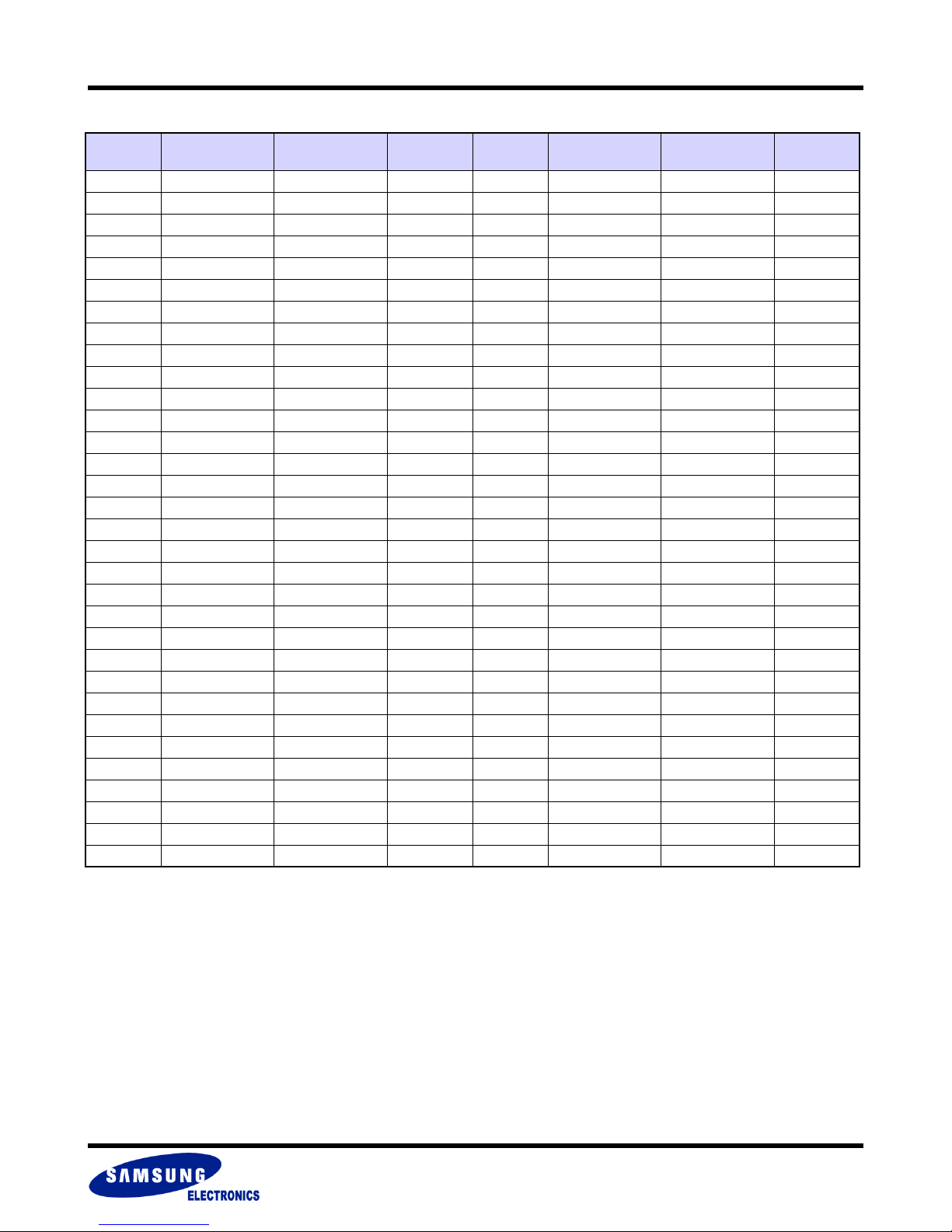
Block Block Address
Block448 01C0h 0000h~00FFh 128KB Block480 01E0h 0000h~00FFh 128KB
Block449 01C1h 0000h~00FFh 128KB Block481 01E1h 0000h~00FFh 128KB
Block450 01C2h 0000h~00FFh 128KB Block482 01E2h 0000h~00FFh 128KB
Block451 01C3h 0000h~00FFh 128KB Block483 01E3h 0000h~00FFh 128KB
Block452 01C4h 0000h~00FFh 128KB Block484 01E4h 0000h~00FFh 128KB
Block453 01C5h 0000h~00FFh 128KB Block485 01E5h 0000h~00FFh 128KB
Block454 01C6h 0000h~00FFh 128KB Block486 01E6h 0000h~00FFh 128KB
Block455 01C7h 0000h~00FFh 128KB Block487 01E7h 0000h~00FFh 128KB
Block456 01C8h 0000h~00FFh 128KB Block488 01E8h 0000h~00FFh 128KB
Block457 01C9h 0000h~00FFh 128KB Block489 01E9h 0000h~00FFh 128KB
Block458 01CAh 0000h~00FFh 128KB Block490 01EAh 0000h~00FFh 128KB
Block459 01CBh 0000h~00FFh 128KB Block491 01EBh 0000h~00FFh 128KB
Block460 01CCh 0000h~00FFh 128KB Block492 01ECh 0000h~00FFh 128KB
Block461 01CDh 0000h~00FFh 128KB Block493 01EDh 0000h~00FFh 128KB
Block462 01CEh 0000h~00FFh 128KB Block494 01EEh 0000h~00FFh 128KB
Block463 01CFh 0000h~00FFh 128KB Block495 01EFh 0000h~00FFh 128KB
Block464 01D0h 0000h~00FFh 128KB Block496 01F0h 0000h~00FFh 128KB
Block465 01D1h 0000h~00FFh 128KB Block497 01F1h 0000h~00FFh 128KB
Block466 01D2h 0000h~00FFh 128KB Block498 01F2h 0000h~00FFh 128KB
Block467 01D3h 0000h~00FFh 128KB Block499 01F3h 0000h~00FFh 128KB
Block468 01D4h 0000h~00FFh 128KB Block500 01F4h 0000h~00FFh 128KB
Block469 01D5h 0000h~00FFh 128KB Block501 01F5h 0000h~00FFh 128KB
Block470 01D6h 0000h~00FFh 128KB Block502 01F6h 0000h~00FFh 128KB
Block471 01D7h 0000h~00FFh 128KB Block503 01F7h 0000h~00FFh 128KB
Block472 01D8h 0000h~00FFh 128KB Block504 01F8h 0000h~00FFh 128KB
Block473 01D9h 0000h~00FFh 128KB Block505 01F9h 0000h~00FFh 128KB
Block474 01DAh 0000h~00FFh 128KB Block506 01FAh 0000h~00FFh 128KB
Block475 01DBh 0000h~00FFh 128KB Block507 01FBh 0000h~00FFh 128KB
Block476 01DCh 0000h~00FFh 128KB Block508 01FCh 0000h~00FFh 128KB
Block477 01DDh 0000h~00FFh 128KB Block509 01FDh 0000h~00FFh 128KB
Block478 01DEh 0000h~00FFh 128KB Block510 01FEh 0000h~00FFh 128KB
Block479 01DFh 0000h~00FFh 128KB Block511 01FFh 0000h~00FFh 128KB
Page and Sector
Address
Size Block Block Address
Page and Sector
Address
Size
- 23 -
Page 24
MuxOneNAND2G(KFM2G16Q2A-DEBx)
MuxOneNAND4G(KFN4G16Q2A-DEBx)
FLASH MEMORY
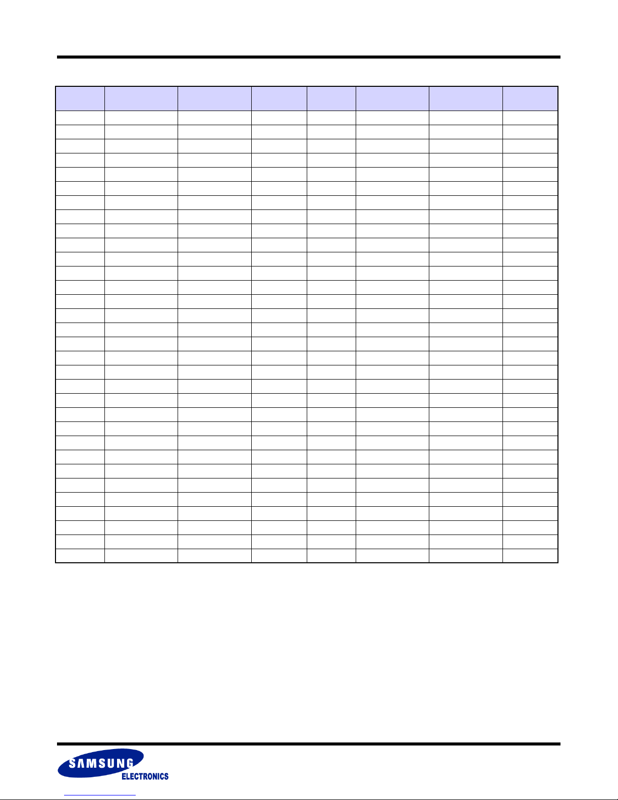
Block Block Address
Block512 0200h 0000h~00FFh 128KB Block544 0220h 0000h~00FFh 128KB
Block513 0201h 0000h~00FFh 128KB Block545 0221h 0000h~00FFh 128KB
Block514 0202h 0000h~00FFh 128KB Block546 0222h 0000h~00FFh 128KB
Block515 0203h 0000h~00FFh 128KB Block547 0223h 0000h~00FFh 128KB
Block516 0204h 0000h~00FFh 128KB Block548 0224h 0000h~00FFh 128KB
Block517 0205h 0000h~00FFh 128KB Block549 0225h 0000h~00FFh 128KB
Block518 0206h 0000h~00FFh 128KB Block550 0226h 0000h~00FFh 128KB
Block519 0207h 0000h~00FFh 128KB Block551 0227h 0000h~00FFh 128KB
Block520 0208h 0000h~00FFh 128KB Block552 0228h 0000h~00FFh 128KB
Block521 0209h 0000h~00FFh 128KB Block553 0229h 0000h~00FFh 128KB
Block522 020Ah 0000h~00FFh 128KB Block554 022Ah 0000h~00FFh 128KB
Block523 020Bh 0000h~00FFh 128KB Block555 022Bh 0000h~00FFh 128KB
Block524 020Ch 0000h~00FFh 128KB Block556 022Ch 0000h~00FFh 128KB
Block525 020Dh 0000h~00FFh 128KB Block557 022Dh 0000h~00FFh 128KB
Block526 020Eh 0000h~00FFh 128KB Block558 022Eh 0000h~00FFh 128KB
Block527 020Fh 0000h~00FFh 128KB Block559 022Fh 0000h~00FFh 128KB
Block528 0210h 0000h~00FFh 128KB Block560 0230h 0000h~00FFh 128KB
Block529 0211h 0000h~00FFh 128KB Block561 0231h 0000h~00FFh 128KB
Block530 0212h 0000h~00FFh 128KB Block562 0232h 0000h~00FFh 128KB
Block531 0213h 0000h~00FFh 128KB Block563 0233h 0000h~00FFh 128KB
Block532 0214h 0000h~00FFh 128KB Block564 0234h 0000h~00FFh 128KB
Block533 0215h 0000h~00FFh 128KB Block565 0235h 0000h~00FFh 128KB
Block534 0216h 0000h~00FFh 128KB Block566 0236h 0000h~00FFh 128KB
Block535 0217h 0000h~00FFh 128KB Block567 0237h 0000h~00FFh 128KB
Block536 0218h 0000h~00FFh 128KB Block568 0238h 0000h~00FFh 128KB
Block537 0219h 0000h~00FFh 128KB Block569 0239h 0000h~00FFh 128KB
Block538 021Ah 0000h~00FFh 128KB Block570 023Ah 0000h~00FFh 128KB
Block539 021Bh 0000h~00FFh 128KB Block571 023Bh 0000h~00FFh 128KB
Block540 021Ch 0000h~00FFh 128KB Block572 023Ch 0000h~00FFh 128KB
Block541 021Dh 0000h~00FFh 128KB Block573 023Dh 0000h~00FFh 128KB
Block542 021Eh 0000h~00FFh 128KB Block574 023Eh 0000h~00FFh 128KB
Block543 021Fh 0000h~00FFh 128KB Block575 023Fh 0000h~00FFh 128KB
Page and Sector
Address
Size Block Block Address
Page and Sector
Address
Size
- 24 -
Page 25
MuxOneNAND2G(KFM2G16Q2A-DEBx)
MuxOneNAND4G(KFN4G16Q2A-DEBx)
FLASH MEMORY
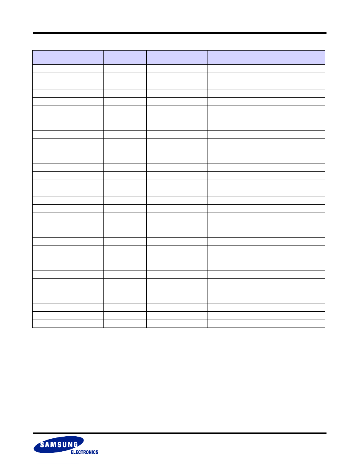
Block Block Address
Block576 0240h 0000h~00FFh 128KB Block608 0260h 0000h~00FFh 128KB
Block577 0241h 0000h~00FFh 128KB Block609 0261h 0000h~00FFh 128KB
Block578 0242h 0000h~00FFh 128KB Block610 0262h 0000h~00FFh 128KB
Block579 0243h 0000h~00FFh 128KB Block611 0263h 0000h~00FFh 128KB
Block580 0244h 0000h~00FFh 128KB Block612 0264h 0000h~00FFh 128KB
Block581 0245h 0000h~00FFh 128KB Block613 0265h 0000h~00FFh 128KB
Block582 0246h 0000h~00FFh 128KB Block614 0266h 0000h~00FFh 128KB
Block583 0247h 0000h~00FFh 128KB Block615 0267h 0000h~00FFh 128KB
Block584 0248h 0000h~00FFh 128KB Block616 0268h 0000h~00FFh 128KB
Block585 0249h 0000h~00FFh 128KB Block617 0269h 0000h~00FFh 128KB
Block586 024Ah 0000h~00FFh 128KB Block618 026Ah 0000h~00FFh 128KB
Block587 024Bh 0000h~00FFh 128KB Block619 026Bh 0000h~00FFh 128KB
Block588 024Ch 0000h~00FFh 128KB Block620 026Ch 0000h~00FFh 128KB
Block589 024Dh 0000h~00FFh 128KB Block621 026Dh 0000h~00FFh 128KB
Block590 024Eh 0000h~00FFh 128KB Block622 026Eh 0000h~00FFh 128KB
Block591 024Fh 0000h~00FFh 128KB Block623 026Fh 0000h~00FFh 128KB
Block592 0250h 0000h~00FFh 128KB Block624 0270h 0000h~00FFh 128KB
Block593 0251h 0000h~00FFh 128KB Block625 0271h 0000h~00FFh 128KB
Block594 0252h 0000h~00FFh 128KB Block626 0272h 0000h~00FFh 128KB
Block595 0253h 0000h~00FFh 128KB Block627 0273h 0000h~00FFh 128KB
Block596 0254h 0000h~00FFh 128KB Block628 0274h 0000h~00FFh 128KB
Block597 0255h 0000h~00FFh 128KB Block629 0275h 0000h~00FFh 128KB
Block598 0256h 0000h~00FFh 128KB Block630 0276h 0000h~00FFh 128KB
Block599 0257h 0000h~00FFh 128KB Block631 0277h 0000h~00FFh 128KB
Block600 0258h 0000h~00FFh 128KB Block632 0278h 0000h~00FFh 128KB
Block601 0259h 0000h~00FFh 128KB Block633 0279h 0000h~00FFh 128KB
Block602 025Ah 0000h~00FFh 128KB Block634 027Ah 0000h~00FFh 128KB
Block603 025Bh 0000h~00FFh 128KB Block635 027Bh 0000h~00FFh 128KB
Block604 025Ch 0000h~00FFh 128KB Block636 027Ch 0000h~00FFh 128KB
Block605 025Dh 0000h~00FFh 128KB Block637 027Dh 0000h~00FFh 128KB
Block606 025Eh 0000h~00FFh 128KB Block638 027Eh 0000h~00FFh 128KB
Block607 025Fh 0000h~00FFh 128KB Block639 027Fh 0000h~00FFh 128KB
Page and Sector
Address
Size Block Block Address
Page and Sector
Address
Size
- 25 -
Page 26
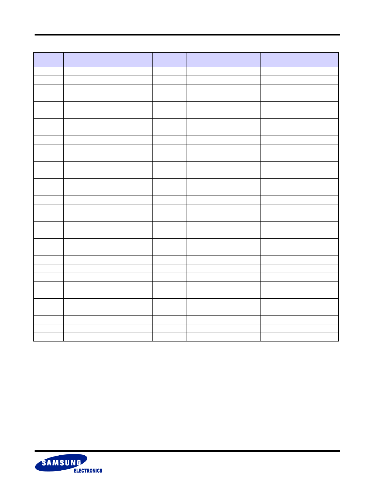
MuxOneNAND2G(KFM2G16Q2A-DEBx)
MuxOneNAND4G(KFN4G16Q2A-DEBx)
FLASH MEMORY
Block Block Address
Block640 0280h 0000h~00FFh 128KB Block672 02A0h 0000h~00FFh 128KB
Block641 0281h 0000h~00FFh 128KB Block673 02A1h 0000h~00FFh 128KB
Block642 0282h 0000h~00FFh 128KB Block674 02A2h 0000h~00FFh 128KB
Block643 0283h 0000h~00FFh 128KB Block675 02A3h 0000h~00FFh 128KB
Block644 0284h 0000h~00FFh 128KB Block676 02A4h 0000h~00FFh 128KB
Block645 0285h 0000h~00FFh 128KB Block677 02A5h 0000h~00FFh 128KB
Block646 0286h 0000h~00FFh 128KB Block678 02A6h 0000h~00FFh 128KB
Block647 0287h 0000h~00FFh 128KB Block679 02A7h 0000h~00FFh 128KB
Block648 0288h 0000h~00FFh 128KB Block680 02A8h 0000h~00FFh 128KB
Block649 0289h 0000h~00FFh 128KB Block681 02A9h 0000h~00FFh 128KB
Block650 028Ah 0000h~00FFh 128KB Block682 02AAh 0000h~00FFh 128KB
Block651 028Bh 0000h~00FFh 128KB Block683 02ABh 0000h~00FFh 128KB
Block652 028Ch 0000h~00FFh 128KB Block684 02ACh 0000h~00FFh 128KB
Block653 028Dh 0000h~00FFh 128KB Block685 02ADh 0000h~00FFh 128KB
Block654 028Eh 0000h~00FFh 128KB Block686 02AEh 0000h~00FFh 128KB
Block655 028Fh 0000h~00FFh 128KB Block687 02AFh 0000h~00FFh 128KB
Block656 0290h 0000h~00FFh 128KB Block688 02B0h 0000h~00FFh 128KB
Block657 0291h 0000h~00FFh 128KB Block689 02B1h 0000h~00FFh 128KB
Block658 0292h 0000h~00FFh 128KB Block690 02B2h 0000h~00FFh 128KB
Block659 0293h 0000h~00FFh 128KB Block691 02B3h 0000h~00FFh 128KB
Block660 0294h 0000h~00FFh 128KB Block692 02B4h 0000h~00FFh 128KB
Block661 0295h 0000h~00FFh 128KB Block693 02B5h 0000h~00FFh 128KB
Block662 0296h 0000h~00FFh 128KB Block694 02B6h 0000h~00FFh 128KB
Block663 0297h 0000h~00FFh 128KB Block695 02B7h 0000h~00FFh 128KB
Block664 0298h 0000h~00FFh 128KB Block696 02B8h 0000h~00FFh 128KB
Block665 0299h 0000h~00FFh 128KB Block697 02B9h 0000h~00FFh 128KB
Block666 029Ah 0000h~00FFh 128KB Block698 02BAh 0000h~00FFh 128KB
Block667 029Bh 0000h~00FFh 128KB Block699 02BBh 0000h~00FFh 128KB
Block668 029Ch 0000h~00FFh 128KB Block700 02BCh 0000h~00FFh 128KB
Block669 029Dh 0000h~00FFh 128KB Block701 02BDh 0000h~00FFh 128KB
Block670 029Eh 0000h~00FFh 128KB Block702 02BEh 0000h~00FFh 128KB
Block671 029Fh 0000h~00FFh 128KB Block703 02BFh 0000h~00FFh 128KB
Page and Sector
Address
Size Block Block Address
Page and Sector
Address
Size
- 26 -
Page 27
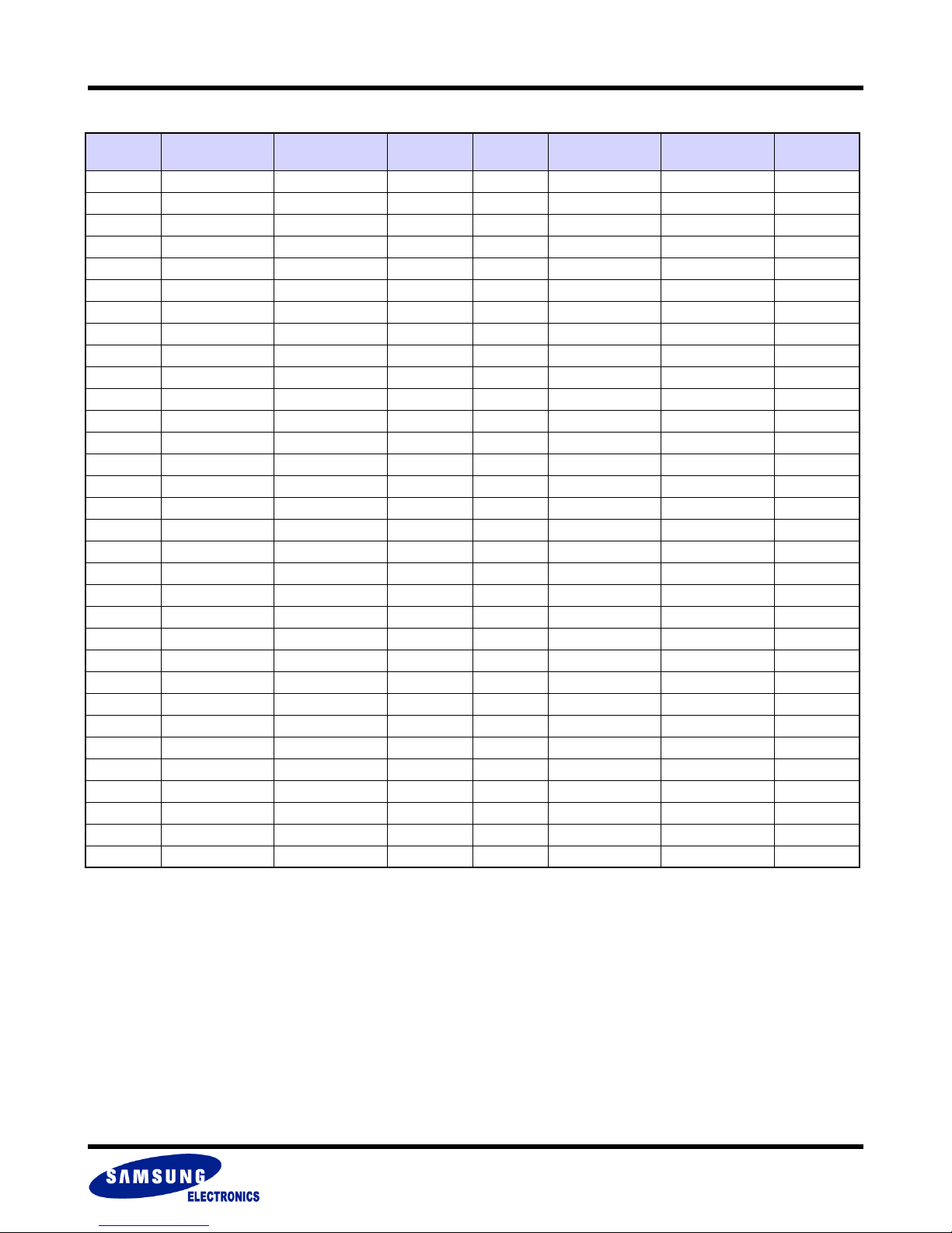
MuxOneNAND2G(KFM2G16Q2A-DEBx)
MuxOneNAND4G(KFN4G16Q2A-DEBx)
FLASH MEMORY
Block Block Address
Block704 02C0h 0000h~00FFh 128KB Block736 02E0h 0000h~00FFh 128KB
Block705 02C1h 0000h~00FFh 128KB Block737 02E1h 0000h~00FFh 128KB
Block706 02C2h 0000h~00FFh 128KB Block738 02E2h 0000h~00FFh 128KB
Block707 02C3h 0000h~00FFh 128KB Block739 02E3h 0000h~00FFh 128KB
Block708 02C4h 0000h~00FFh 128KB Block740 02E4h 0000h~00FFh 128KB
Block709 02C5h 0000h~00FFh 128KB Block741 02E5h 0000h~00FFh 128KB
Block710 02C6h 0000h~00FFh 128KB Block742 02E6h 0000h~00FFh 128KB
Block711 02C7h 0000h~00FFh 128KB Block743 02E7h 0000h~00FFh 128KB
Block712 02C8h 0000h~00FFh 128KB Block744 02E8h 0000h~00FFh 128KB
Block713 02C9h 0000h~00FFh 128KB Block745 02E9h 0000h~00FFh 128KB
Block714 02CAh 0000h~00FFh 128KB Block746 02EAh 0000h~00FFh 128KB
Block715 02CBh 0000h~00FFh 128KB Block747 02EBh 0000h~00FFh 128KB
Block716 02CCh 0000h~00FFh 128KB Block748 02ECh 0000h~00FFh 128KB
Block717 02CDh 0000h~00FFh 128KB Block749 02EDh 0000h~00FFh 128KB
Block718 02CEh 0000h~00FFh 128KB Block750 02EEh 0000h~00FFh 128KB
Block719 02CFh 0000h~00FFh 128KB Block751 02EFh 0000h~00FFh 128KB
Block720 02D0h 0000h~00FFh 128KB Block752 02F0h 0000h~00FFh 128KB
Block721 02D1h 0000h~00FFh 128KB Block753 02F1h 0000h~00FFh 128KB
Block722 02D2h 0000h~00FFh 128KB Block754 02F2h 0000h~00FFh 128KB
Block723 02D3h 0000h~00FFh 128KB Block755 02F3h 0000h~00FFh 128KB
Block724 02D4h 0000h~00FFh 128KB Block756 02F4h 0000h~00FFh 128KB
Block725 02D5h 0000h~00FFh 128KB Block757 02F5h 0000h~00FFh 128KB
Block726 02D6h 0000h~00FFh 128KB Block758 02F6h 0000h~00FFh 128KB
Block727 02D7h 0000h~00FFh 128KB Block759 02F7h 0000h~00FFh 128KB
Block728 02D8h 0000h~00FFh 128KB Block760 02F8h 0000h~00FFh 128KB
Block729 02D9h 0000h~00FFh 128KB Block761 02F9h 0000h~00FFh 128KB
Block730 02DAh 0000h~00FFh 128KB Block762 02FAh 0000h~00FFh 128KB
Block731 02DBh 0000h~00FFh 128KB Block763 02FBh 0000h~00FFh 128KB
Block732 02DCh 0000h~00FFh 128KB Block764 02FCh 0000h~00FFh 128KB
Block733 02DDh 0000h~00FFh 128KB Block765 02FDh 0000h~00FFh 128KB
Block734 02DEh 0000h~00FFh 128KB Block766 02FEh 0000h~00FFh 128KB
Block735 02DFh 0000h~00FFh 128KB Block767 02FFh 0000h~00FFh 128KB
Page and Sector
Address
Size Block Block Address
Page and Sector
Address
Size
- 27 -
Page 28
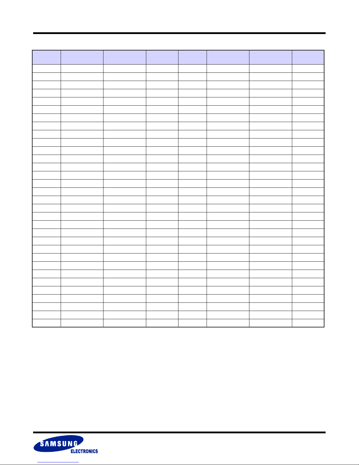
MuxOneNAND2G(KFM2G16Q2A-DEBx)
MuxOneNAND4G(KFN4G16Q2A-DEBx)
FLASH MEMORY
Block Block Address
Block768 0300h 0000h~00FFh 128KB Block800 0320h 0000h~00FFh 128KB
Block769 0301h 0000h~00FFh 128KB Block801 0321h 0000h~00FFh 128KB
Block770 0302h 0000h~00FFh 128KB Block802 0322h 0000h~00FFh 128KB
Block771 0303h 0000h~00FFh 128KB Block803 0323h 0000h~00FFh 128KB
Block772 0304h 0000h~00FFh 128KB Block804 0324h 0000h~00FFh 128KB
Block773 0305h 0000h~00FFh 128KB Block805 0325h 0000h~00FFh 128KB
Block774 0306h 0000h~00FFh 128KB Block806 0326h 0000h~00FFh 128KB
Block775 0307h 0000h~00FFh 128KB Block807 0327h 0000h~00FFh 128KB
Block776 0308h 0000h~00FFh 128KB Block808 0328h 0000h~00FFh 128KB
Block777 0309h 0000h~00FFh 128KB Block809 0329h 0000h~00FFh 128KB
Block778 030Ah 0000h~00FFh 128KB Block810 032Ah 0000h~00FFh 128KB
Block779 030Bh 0000h~00FFh 128KB Block811 032Bh 0000h~00FFh 128KB
Block780 030Ch 0000h~00FFh 128KB Block812 032Ch 0000h~00FFh 128KB
Block781 030Dh 0000h~00FFh 128KB Block813 032Dh 0000h~00FFh 128KB
Block782 030Eh 0000h~00FFh 128KB Block814 032Eh 0000h~00FFh 128KB
Block783 030Fh 0000h~00FFh 128KB Block815 032Fh 0000h~00FFh 128KB
Block784 0310h 0000h~00FFh 128KB Block816 0330h 0000h~00FFh 128KB
Block785 0311h 0000h~00FFh 128KB Block817 0331h 0000h~00FFh 128KB
Block786 0312h 0000h~00FFh 128KB Block818 0332h 0000h~00FFh 128KB
Block787 0313h 0000h~00FFh 128KB Block819 0333h 0000h~00FFh 128KB
Block788 0314h 0000h~00FFh 128KB Block820 0334h 0000h~00FFh 128KB
Block789 0315h 0000h~00FFh 128KB Block821 0335h 0000h~00FFh 128KB
Block790 0316h 0000h~00FFh 128KB Block822 0336h 0000h~00FFh 128KB
Block791 0317h 0000h~00FFh 128KB Block823 0337h 0000h~00FFh 128KB
Block792 0318h 0000h~00FFh 128KB Block824 0338h 0000h~00FFh 128KB
Block793 0319h 0000h~00FFh 128KB Block825 0339h 0000h~00FFh 128KB
Block794 031Ah 0000h~00FFh 128KB Block826 033Ah 0000h~00FFh 128KB
Block795 031Bh 0000h~00FFh 128KB Block827 033Bh 0000h~00FFh 128KB
Block796 031Ch 0000h~00FFh 128KB Block828 033Ch 0000h~00FFh 128KB
Block797 031Dh 0000h~00FFh 128KB Block829 033Dh 0000h~00FFh 128KB
Block798 031Eh 0000h~00FFh 128KB Block830 033Eh 0000h~00FFh 128KB
Block799 031Fh 0000h~00FFh 128KB Block831 033Fh 0000h~00FFh 128KB
Page and Sector
Address
Size Block Block Address
Page and Sector
Address
Size
- 28 -
Page 29
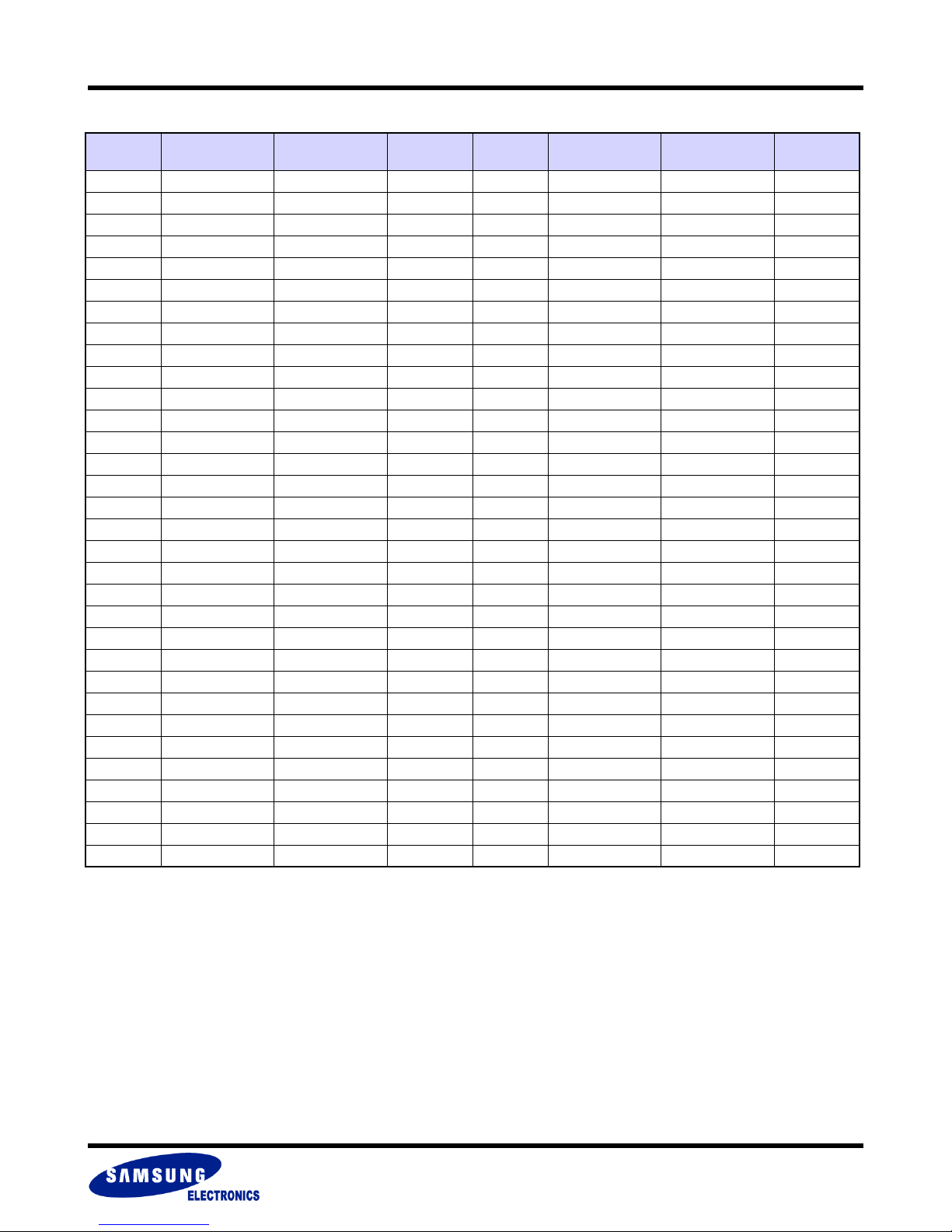
MuxOneNAND2G(KFM2G16Q2A-DEBx)
MuxOneNAND4G(KFN4G16Q2A-DEBx)
FLASH MEMORY
Block Block Address
Block832 0340h 0000h~00FFh 128KB Block864 0360h 0000h~00FFh 128KB
Block833 0341h 0000h~00FFh 128KB Block865 0361h 0000h~00FFh 128KB
Block834 0342h 0000h~00FFh 128KB Block866 0362h 0000h~00FFh 128KB
Block835 0343h 0000h~00FFh 128KB Block867 0363h 0000h~00FFh 128KB
Block836 0344h 0000h~00FFh 128KB Block868 0364h 0000h~00FFh 128KB
Block837 0345h 0000h~00FFh 128KB Block869 0365h 0000h~00FFh 128KB
Block838 0346h 0000h~00FFh 128KB Block870 0366h 0000h~00FFh 128KB
Block839 0347h 0000h~00FFh 128KB Block871 0367h 0000h~00FFh 128KB
Block840 0348h 0000h~00FFh 128KB Block872 0368h 0000h~00FFh 128KB
Block841 0349h 0000h~00FFh 128KB Block873 0369h 0000h~00FFh 128KB
Block842 034Ah 0000h~00FFh 128KB Block874 036Ah 0000h~00FFh 128KB
Block843 034Bh 0000h~00FFh 128KB Block875 036Bh 0000h~00FFh 128KB
Block844 034Ch 0000h~00FFh 128KB Block876 036Ch 0000h~00FFh 128KB
Block845 034Dh 0000h~00FFh 128KB Block877 036Dh 0000h~00FFh 128KB
Block846 034Eh 0000h~00FFh 128KB Block878 036Eh 0000h~00FFh 128KB
Block847 034Fh 0000h~00FFh 128KB Block879 036Fh 0000h~00FFh 128KB
Block848 0350h 0000h~00FFh 128KB Block880 0370h 0000h~00FFh 128KB
Block849 0351h 0000h~00FFh 128KB Block881 0371h 0000h~00FFh 128KB
Block850 0352h 0000h~00FFh 128KB Block882 0372h 0000h~00FFh 128KB
Block851 0353h 0000h~00FFh 128KB Block883 0373h 0000h~00FFh 128KB
Block852 0354h 0000h~00FFh 128KB Block884 0374h 0000h~00FFh 128KB
Block853 0355h 0000h~00FFh 128KB Block885 0375h 0000h~00FFh 128KB
Block854 0356h 0000h~00FFh 128KB Block886 0376h 0000h~00FFh 128KB
Block855 0357h 0000h~00FFh 128KB Block887 0377h 0000h~00FFh 128KB
Block856 0358h 0000h~00FFh 128KB Block888 0378h 0000h~00FFh 128KB
Block857 0359h 0000h~00FFh 128KB Block889 0379h 0000h~00FFh 128KB
Block858 035Ah 0000h~00FFh 128KB Block890 037Ah 0000h~00FFh 128KB
Block859 035Bh 0000h~00FFh 128KB Block891 037Bh 0000h~00FFh 128KB
Block860 035Ch 0000h~00FFh 128KB Block892 037Ch 0000h~00FFh 128KB
Block861 035Dh 0000h~00FFh 128KB Block893 037Dh 0000h~00FFh 128KB
Block862 035Eh 0000h~00FFh 128KB Block894 037Eh 0000h~00FFh 128KB
Block863 035Fh 0000h~00FFh 128KB Block895 037Fh 0000h~00FFh 128KB
Page and Sector
Address
Size Block Block Address
Page and Sector
Address
Size
- 29 -
Page 30
MuxOneNAND2G(KFM2G16Q2A-DEBx)
MuxOneNAND4G(KFN4G16Q2A-DEBx)
FLASH MEMORY
Block Block Address
Block896 0380h 0000h~00FFh 128KB Block928 03A0h 0000h~00FFh 128KB
Block897 0381h 0000h~00FFh 128KB Block929 03A1h 0000h~00FFh 128KB
Block898 0382h 0000h~00FFh 128KB Block930 03A2h 0000h~00FFh 128KB
Block899 0383h 0000h~00FFh 128KB Block931 03A3h 0000h~00FFh 128KB
Block900 0384h 0000h~00FFh 128KB Block932 03A4h 0000h~00FFh 128KB
Block901 0385h 0000h~00FFh 128KB Block933 03A5h 0000h~00FFh 128KB
Block902 0386h 0000h~00FFh 128KB Block934 03A6h 0000h~00FFh 128KB
Block903 0387h 0000h~00FFh 128KB Block935 03A7h 0000h~00FFh 128KB
Block904 0388h 0000h~00FFh 128KB Block936 03A8h 0000h~00FFh 128KB
Block905 0389h 0000h~00FFh 128KB Block937 03A9h 0000h~00FFh 128KB
Block906 038Ah 0000h~00FFh 128KB Block938 03AAh 0000h~00FFh 128KB
Block907 038Bh 0000h~00FFh 128KB Block939 03ABh 0000h~00FFh 128KB
Block908 038Ch 0000h~00FFh 128KB Block940 03ACh 0000h~00FFh 128KB
Block909 038Dh 0000h~00FFh 128KB Block941 03ADh 0000h~00FFh 128KB
Block910 038Eh 0000h~00FFh 128KB Block942 03AEh 0000h~00FFh 128KB
Block911 038Fh 0000h~00FFh 128KB Block943 03AFh 0000h~00FFh 128KB
Block912 0390h 0000h~00FFh 128KB Block944 03B0h 0000h~00FFh 128KB
Block913 0391h 0000h~00FFh 128KB Block945 03B1h 0000h~00FFh 128KB
Block914 0392h 0000h~00FFh 128KB Block946 03B2h 0000h~00FFh 128KB
Block915 0393h 0000h~00FFh 128KB Block947 03B3h 0000h~00FFh 128KB
Block916 0394h 0000h~00FFh 128KB Block948 03B4h 0000h~00FFh 128KB
Block917 0395h 0000h~00FFh 128KB Block949 03B5h 0000h~00FFh 128KB
Block918 0396h 0000h~00FFh 128KB Block950 03B6h 0000h~00FFh 128KB
Block919 0397h 0000h~00FFh 128KB Block951 03B7h 0000h~00FFh 128KB
Block920 0398h 0000h~00FFh 128KB Block952 03B8h 0000h~00FFh 128KB
Block921 0399h 0000h~00FFh 128KB Block953 03B9h 0000h~00FFh 128KB
Block922 039Ah 0000h~00FFh 128KB Block954 03BAh 0000h~00FFh 128KB
Block923 039Bh 0000h~00FFh 128KB Block955 03BBh 0000h~00FFh 128KB
Block924 039Ch 0000h~00FFh 128KB Block956 03BCh 0000h~00FFh 128KB
Block925 039Dh 0000h~00FFh 128KB Block957 03BDh 0000h~00FFh 128KB
Block926 039Eh 0000h~00FFh 128KB Block958 03BEh 0000h~00FFh 128KB
Block927 039Fh 0000h~00FFh 128KB Block959 03BFh 0000h~00FFh 128KB
Page and Sector
Address
Size Block Block Address
Page and Sector
Address
Size
- 30 -
Page 31
MuxOneNAND2G(KFM2G16Q2A-DEBx)
MuxOneNAND4G(KFN4G16Q2A-DEBx)
FLASH MEMORY
Block Block Address
Block960 03C0h 0000h~00FFh 128KB Block992 03E0h 0000h~00FFh 128KB
Block961 03C1h 0000h~00FFh 128KB Block993 03E1h 0000h~00FFh 128KB
Block962 03C2h 0000h~00FFh 128KB Block994 03E2h 0000h~00FFh 128KB
Block963 03C3h 0000h~00FFh 128KB Block995 03E3h 0000h~00FFh 128KB
Block964 03C4h 0000h~00FFh 128KB Block996 03E4h 0000h~00FFh 128KB
Block965 03C5h 0000h~00FFh 128KB Block997 03E5h 0000h~00FFh 128KB
Block966 03C6h 0000h~00FFh 128KB Block998 03E6h 0000h~00FFh 128KB
Block967 03C7h 0000h~00FFh 128KB Block999 03E7h 0000h~00FFh 128KB
Block968 03C8h 0000h~00FFh 128KB Block1000 03E8h 0000h~00FFh 128KB
Block969 03C9h 0000h~00FFh 128KB Block1001 03E9h 0000h~00FFh 128KB
Block970 03CAh 0000h~00FFh 128KB Block1002 03EAh 0000h~00FFh 128KB
Block971 03CBh 0000h~00FFh 128KB Block1003 03EBh 0000h~00FFh 128KB
Block972 03CCh 0000h~00FFh 128KB Block1004 03ECh 0000h~00FFh 128KB
Block973 03CDh 0000h~00FFh 128KB Block1005 03EDh 0000h~00FFh 128KB
Block974 03CEh 0000h~00FFh 128KB Block1006 03EEh 0000h~00FFh 128KB
Block975 03CFh 0000h~00FFh 128KB Block1007 03EFh 0000h~00FFh 128KB
Block976 03D0h 0000h~00FFh 128KB Block1008 03F0h 0000h~00FFh 128KB
Block977 03D1h 0000h~00FFh 128KB Block1009 03F1h 0000h~00FFh 128KB
Block978 03D2h 0000h~00FFh 128KB Block1010 03F2h 0000h~00FFh 128KB
Block979 03D3h 0000h~00FFh 128KB Block1011 03F3h 0000h~00FFh 128KB
Block980 03D4h 0000h~00FFh 128KB Block1012 03F4h 0000h~00FFh 128KB
Block981 03D5h 0000h~00FFh 128KB Block1013 03F5h 0000h~00FFh 128KB
Block982 03D6h 0000h~00FFh 128KB Block1014 03F6h 0000h~00FFh 128KB
Block983 03D7h 0000h~00FFh 128KB Block1015 03F7h 0000h~00FFh 128KB
Block984 03D8h 0000h~00FFh 128KB Block1016 03F8h 0000h~00FFh 128KB
Block985 03D9h 0000h~00FFh 128KB Block1017 03F9h 0000h~00FFh 128KB
Block986 03DAh 0000h~00FFh 128KB Block1018 03FAh 0000h~00FFh 128KB
Block987 03DBh 0000h~00FFh 128KB Block1019 03FBh 0000h~00FFh 128KB
Block988 03DCh 0000h~00FFh 128KB Block1020 03FCh 0000h~00FFh 128KB
Block989 03DDh 0000h~00FFh 128KB Block1021 03FDh 0000h~00FFh 128KB
Block990 03DEh 0000h~00FFh 128KB Block1022 03FEh 0000h~00FFh 128KB
Block991 03DFh 0000h~00FFh 128KB Block1023 03FFh 0000h~00FFh 128KB
Page and Sector
Address
Size Block Block Address
Page and Sector
Address
Size
- 31 -
Page 32
MuxOneNAND2G(KFM2G16Q2A-DEBx)
MuxOneNAND4G(KFN4G16Q2A-DEBx)
FLASH MEMORY
Block Block Address
Block1024 0400h 0000h~00FFh 128KB Block1056 0420h 0000h~00FFh 128KB
Block1025 0401h 0000h~00FFh 128KB Block1057 0421h 0000h~00FFh 128KB
Block1026 0402h 0000h~00FFh 128KB Block1058 0422h 0000h~00FFh 128KB
Block1027 0403h 0000h~00FFh 128KB Block1059 0423h 0000h~00FFh 128KB
Block1028 0404h 0000h~00FFh 128KB Block1060 0424h 0000h~00FFh 128KB
Block1029 0405h 0000h~00FFh 128KB Block1061 0425h 0000h~00FFh 128KB
Block1030 0406h 0000h~00FFh 128KB Block1062 0426h 0000h~00FFh 128KB
Block1031 0407h 0000h~00FFh 128KB Block1063 0427h 0000h~00FFh 128KB
Block1032 0408h 0000h~00FFh 128KB Block1064 0428h 0000h~00FFh 128KB
Block1033 0409h 0000h~00FFh 128KB Block1065 0429h 0000h~00FFh 128KB
Block1034 040Ah 0000h~00FFh 128KB Block1066 042Ah 0000h~00FFh 128KB
Block1035 040Bh 0000h~00FFh 128KB Block1067 042Bh 0000h~00FFh 128KB
Block1036 040Ch 0000h~00FFh 128KB Block1068 042Ch 0000h~00FFh 128KB
Block1037 040Dh 0000h~00FFh 128KB Block1069 042Dh 0000h~00FFh 128KB
Block1038 040Eh 0000h~00FFh 128KB Block1070 042Eh 0000h~00FFh 128KB
Block1039 040Fh 0000h~00FFh 128KB Block1071 042Fh 0000h~00FFh 128KB
Block1040 0410h 0000h~00FFh 128KB Block1072 0430h 0000h~00FFh 128KB
Block1041 0411h 0000h~00FFh 128KB Block1073 0431h 0000h~00FFh 128KB
Block1042 0412h 0000h~00FFh 128KB Block1074 0432h 0000h~00FFh 128KB
Block1043 0413h 0000h~00FFh 128KB Block1075 0433h 0000h~00FFh 128KB
Block1044 0414h 0000h~00FFh 128KB Block1076 0434h 0000h~00FFh 128KB
Block1045 0415h 0000h~00FFh 128KB Block1077 0435h 0000h~00FFh 128KB
Block1046 0416h 0000h~00FFh 128KB Block1078 0436h 0000h~00FFh 128KB
Block1047 0417h 0000h~00FFh 128KB Block1079 0437h 0000h~00FFh 128KB
Block1048 0418h 0000h~00FFh 128KB Block1080 0438h 0000h~00FFh 128KB
Block1049 0419h 0000h~00FFh 128KB Block1081 0439h 0000h~00FFh 128KB
Block1050 041Ah 0000h~00FFh 128KB Block1082 043Ah 0000h~00FFh 128KB
Block1051 041Bh 0000h~00FFh 128KB Block1083 043Bh 0000h~00FFh 128KB
Block1052 041Ch 0000h~00FFh 128KB Block1084 043Ch 0000h~00FFh 128KB
Block1053 041Dh 0000h~00FFh 128KB Block1085 043Dh 0000h~00FFh 128KB
Block1054 041Eh 0000h~00FFh 128KB Block1086 043Eh 0000h~00FFh 128KB
Block1055 041Fh 0000h~00FFh 128KB Block1087 043Fh 0000h~00FFh 128KB
Page and Sector
Address
Size Block Block Address
Page and Sector
Address
Size
- 32 -
Page 33
MuxOneNAND2G(KFM2G16Q2A-DEBx)
MuxOneNAND4G(KFN4G16Q2A-DEBx)
FLASH MEMORY
Block Block Address
Block1088 0440h 0000h~00FFh 128KB Block1120 0460h 0000h~00FFh 128KB
Block1089 0441h 0000h~00FFh 128KB Block1121 0461h 0000h~00FFh 128KB
Block1090 0442h 0000h~00FFh 128KB Block1122 0462h 0000h~00FFh 128KB
Block1091 0443h 0000h~00FFh 128KB Block1123 0463h 0000h~00FFh 128KB
Block1092 0444h 0000h~00FFh 128KB Block1124 0464h 0000h~00FFh 128KB
Block1093 0445h 0000h~00FFh 128KB Block1125 0465h 0000h~00FFh 128KB
Block1094 0446h 0000h~00FFh 128KB Block1126 0466h 0000h~00FFh 128KB
Block1095 0447h 0000h~00FFh 128KB Block1127 0467h 0000h~00FFh 128KB
Block1096 0448h 0000h~00FFh 128KB Block1128 0468h 0000h~00FFh 128KB
Block1097 0449h 0000h~00FFh 128KB Block1129 0469h 0000h~00FFh 128KB
Block1098 044Ah 0000h~00FFh 128KB Block1130 046Ah 0000h~00FFh 128KB
Block1099 044Bh 0000h~00FFh 128KB Block1131 046Bh 0000h~00FFh 128KB
Block1100 044Ch 0000h~00FFh 128KB Block1132 046Ch 0000h~00FFh 128KB
Block1101 044Dh 0000h~00FFh 128KB Block1133 046Dh 0000h~00FFh 128KB
Block1102 044Eh 0000h~00FFh 128KB Block1134 046Eh 0000h~00FFh 128KB
Block1103 044Fh 0000h~00FFh 128KB Block1135 046Fh 0000h~00FFh 128KB
Block1104 0450h 0000h~00FFh 128KB Block1136 0470h 0000h~00FFh 128KB
Block1105 0451h 0000h~00FFh 128KB Block1137 0471h 0000h~00FFh 128KB
Block1106 0452h 0000h~00FFh 128KB Block1138 0472h 0000h~00FFh 128KB
Block1107 0453h 0000h~00FFh 128KB Block1139 0473h 0000h~00FFh 128KB
Block1108 0454h 0000h~00FFh 128KB Block1140 0474h 0000h~00FFh 128KB
Block1109 0455h 0000h~00FFh 128KB Block1141 0475h 0000h~00FFh 128KB
Block1110 0456h 0000h~00FFh 128KB Block1142 0476h 0000h~00FFh 128KB
Block1111 0457h 0000h~00FFh 128KB Block1143 0477h 0000h~00FFh 128KB
Block1112 0458h 0000h~00FFh 128KB Block1144 0478h 0000h~00FFh 128KB
Block1113 0459h 0000h~00FFh 128KB Block1145 0479h 0000h~00FFh 128KB
Block1114 045Ah 0000h~00FFh 128KB Block1146 047Ah 0000h~00FFh 128KB
Block1115 045Bh 0000h~00FFh 128KB Block1147 047Bh 0000h~00FFh 128KB
Block1116 045Ch 0000h~00FFh 128KB Block1148 047Ch 0000h~00FFh 128KB
Block1117 045Dh 0000h~00FFh 128KB Block1149 047Dh 0000h~00FFh 128KB
Block1118 045Eh 0000h~00FFh 128KB Block1150 047Eh 0000h~00FFh 128KB
Block1119 045Fh 0000h~00FFh 128KB Block1151 047Fh 0000h~00FFh 128KB
Page and Sector
Address
Size Block Block Address
Page and Sector
Address
Size
- 33 -
Page 34
MuxOneNAND2G(KFM2G16Q2A-DEBx)
MuxOneNAND4G(KFN4G16Q2A-DEBx)
FLASH MEMORY
Block Block Address
Block1152 0480h 0000h~00FFh 128KB Block1184 04A0h 0000h~00FFh 128KB
Block1153 0481h 0000h~00FFh 128KB Block1185 04A1h 0000h~00FFh 128KB
Block1154 0482h 0000h~00FFh 128KB Block1186 04A2h 0000h~00FFh 128KB
Block1155 0483h 0000h~00FFh 128KB Block1187 04A3h 0000h~00FFh 128KB
Block1156 0484h 0000h~00FFh 128KB Block1188 04A4h 0000h~00FFh 128KB
Block1157 0485h 0000h~00FFh 128KB Block1189 04A5h 0000h~00FFh 128KB
Block1158 0486h 0000h~00FFh 128KB Block1190 04A6h 0000h~00FFh 128KB
Block1159 0487h 0000h~00FFh 128KB Block1191 04A7h 0000h~00FFh 128KB
Block1160 0488h 0000h~00FFh 128KB Block1192 04A8h 0000h~00FFh 128KB
Block1161 0489h 0000h~00FFh 128KB Block1193 04A9h 0000h~00FFh 128KB
Block1162 048Ah 0000h~00FFh 128KB Block1194 04AAh 0000h~00FFh 128KB
Block1163 048Bh 0000h~00FFh 128KB Block1195 04ABh 0000h~00FFh 128KB
Block1164 048Ch 0000h~00FFh 128KB Block1196 04ACh 0000h~00FFh 128KB
Block1165 048Dh 0000h~00FFh 128KB Block1197 04ADh 0000h~00FFh 128KB
Block1166 048Eh 0000h~00FFh 128KB Block1198 04AEh 0000h~00FFh 128KB
Block1167 048Fh 0000h~00FFh 128KB Block1199 04AFh 0000h~00FFh 128KB
Block1168 0490h 0000h~00FFh 128KB Block1200 04B0h 0000h~00FFh 128KB
Block1169 0491h 0000h~00FFh 128KB Block1201 04B1h 0000h~00FFh 128KB
Block1170 0492h 0000h~00FFh 128KB Block1202 04B2h 0000h~00FFh 128KB
Block1171 0493h 0000h~00FFh 128KB Block1203 04B3h 0000h~00FFh 128KB
Block1172 0494h 0000h~00FFh 128KB Block1204 04B4h 0000h~00FFh 128KB
Block1173 0495h 0000h~00FFh 128KB Block1205 04B5h 0000h~00FFh 128KB
Block1174 0496h 0000h~00FFh 128KB Block1206 04B6h 0000h~00FFh 128KB
Block1175 0497h 0000h~00FFh 128KB Block1207 04B7h 0000h~00FFh 128KB
Block1176 0498h 0000h~00FFh 128KB Block1208 04B8h 0000h~00FFh 128KB
Block1177 0499h 0000h~00FFh 128KB Block1209 04B9h 0000h~00FFh 128KB
Block1178 049Ah 0000h~00FFh 128KB Block1210 04BAh 0000h~00FFh 128KB
Block1179 049Bh 0000h~00FFh 128KB Block1211 04BBh 0000h~00FFh 128KB
Block1180 049Ch 0000h~00FFh 128KB Block1212 04BCh 0000h~00FFh 128KB
Block1181 049Dh 0000h~00FFh 128KB Block1213 04BDh 0000h~00FFh 128KB
Block1182 049Eh 0000h~00FFh 128KB Block1214 04BEh 0000h~00FFh 128KB
Block1183 049Fh 0000h~00FFh 128KB Block1215 04BFh 0000h~00FFh 128KB
Page and Sector
Address
Size Block Block Address
Page and Sector
Address
Size
- 34 -
Page 35
MuxOneNAND2G(KFM2G16Q2A-DEBx)
MuxOneNAND4G(KFN4G16Q2A-DEBx)
FLASH MEMORY
Block Block Address
Block1216 04C0h 0000h~00FFh 128KB Block1248 04E0h 0000h~00FFh 128KB
Block1217 04C1h 0000h~00FFh 128KB Block1249 04E1h 0000h~00FFh 128KB
Block1218 04C2h 0000h~00FFh 128KB Block1250 04E2h 0000h~00FFh 128KB
Block1219 04C3h 0000h~00FFh 128KB Block1251 04E3h 0000h~00FFh 128KB
Block1220 04C4h 0000h~00FFh 128KB Block1252 04E4h 0000h~00FFh 128KB
Block1221 04C5h 0000h~00FFh 128KB Block1253 04E5h 0000h~00FFh 128KB
Block1222 04C6h 0000h~00FFh 128KB Block1254 04E6h 0000h~00FFh 128KB
Block1223 04C7h 0000h~00FFh 128KB Block1255 04E7h 0000h~00FFh 128KB
Block1224 04C8h 0000h~00FFh 128KB Block1256 04E8h 0000h~00FFh 128KB
Block1225 04C9h 0000h~00FFh 128KB Block1257 04E9h 0000h~00FFh 128KB
Block1226 04CAh 0000h~00FFh 128KB Block1258 04EAh 0000h~00FFh 128KB
Block1227 04CBh 0000h~00FFh 128KB Block1259 04EBh 0000h~00FFh 128KB
Block1228 04CCh 0000h~00FFh 128KB Block1260 04ECh 0000h~00FFh 128KB
Block1229 04CDh 0000h~00FFh 128KB Block1261 04EDh 0000h~00FFh 128KB
Block1230 04CEh 0000h~00FFh 128KB Block1262 04EEh 0000h~00FFh 128KB
Block1231 04CFh 0000h~00FFh 128KB Block1263 04EFh 0000h~00FFh 128KB
Block1232 04D0h 0000h~00FFh 128KB Block1264 04F0h 0000h~00FFh 128KB
Block1233 04D1h 0000h~00FFh 128KB Block1265 04F1h 0000h~00FFh 128KB
Block1234 04D2h 0000h~00FFh 128KB Block1266 04F2h 0000h~00FFh 128KB
Block1235 04D3h 0000h~00FFh 128KB Block1267 04F3h 0000h~00FFh 128KB
Block1236 04D4h 0000h~00FFh 128KB Block1268 04F4h 0000h~00FFh 128KB
Block1237 04D5h 0000h~00FFh 128KB Block1269 04F5h 0000h~00FFh 128KB
Block1238 04D6h 0000h~00FFh 128KB Block1270 04F6h 0000h~00FFh 128KB
Block1239 04D7h 0000h~00FFh 128KB Block1271 04F7h 0000h~00FFh 128KB
Block1240 04D8h 0000h~00FFh 128KB Block1272 04F8h 0000h~00FFh 128KB
Block1241 04D9h 0000h~00FFh 128KB Block1273 04F9h 0000h~00FFh 128KB
Block1242 04DAh 0000h~00FFh 128KB Block1274 04FAh 0000h~00FFh 128KB
Block1243 04DBh 0000h~00FFh 128KB Block1275 04FBh 0000h~00FFh 128KB
Block1244 04DCh 0000h~00FFh 128KB Block1276 04FCh 0000h~00FFh 128KB
Block1245 04DDh 0000h~00FFh 128KB Block1277 04FDh 0000h~00FFh 128KB
Block1246 04DEh 0000h~00FFh 128KB Block1278 04FEh 0000h~00FFh 128KB
Block1247 04DFh 0000h~00FFh 128KB Block1279 04FFh 0000h~00FFh 128KB
Page and Sector
Address
Size Block Block Address
Page and Sector
Address
Size
- 35 -
Page 36
MuxOneNAND2G(KFM2G16Q2A-DEBx)
MuxOneNAND4G(KFN4G16Q2A-DEBx)
FLASH MEMORY
Block Block Address
Block1280 0500h 0000h~00FFh 128KB Block1312 0520h 0000h~00FFh 128KB
Block1281 0501h 0000h~00FFh 128KB Block1313 0521h 0000h~00FFh 128KB
Block1282 0502h 0000h~00FFh 128KB Block1314 0522h 0000h~00FFh 128KB
Block1283 0503h 0000h~00FFh 128KB Block1315 0523h 0000h~00FFh 128KB
Block1284 0504h 0000h~00FFh 128KB Block1316 0524h 0000h~00FFh 128KB
Block1285 0505h 0000h~00FFh 128KB Block1317 0525h 0000h~00FFh 128KB
Block1286 0506h 0000h~00FFh 128KB Block1318 0526h 0000h~00FFh 128KB
Block1287 0507h 0000h~00FFh 128KB Block1319 0527h 0000h~00FFh 128KB
Block1288 0508h 0000h~00FFh 128KB Block1320 0528h 0000h~00FFh 128KB
Block1289 0509h 0000h~00FFh 128KB Block1321 0529h 0000h~00FFh 128KB
Block1290 050Ah 0000h~00FFh 128KB Block1322 052Ah 0000h~00FFh 128KB
Block1291 050Bh 0000h~00FFh 128KB Block1323 052Bh 0000h~00FFh 128KB
Block1292 050Ch 0000h~00FFh 128KB Block1324 052Ch 0000h~00FFh 128KB
Block1293 050Dh 0000h~00FFh 128KB Block1325 052Dh 0000h~00FFh 128KB
Block1294 050Eh 0000h~00FFh 128KB Block1326 052Eh 0000h~00FFh 128KB
Block1295 050Fh 0000h~00FFh 128KB Block1327 052Fh 0000h~00FFh 128KB
Block1296 0510h 0000h~00FFh 128KB Block1328 0530h 0000h~00FFh 128KB
Block1297 0511h 0000h~00FFh 128KB Block1329 0531h 0000h~00FFh 128KB
Block1298 0512h 0000h~00FFh 128KB Block1330 0532h 0000h~00FFh 128KB
Block1299 0513h 0000h~00FFh 128KB Block1331 0533h 0000h~00FFh 128KB
Block1300 0514h 0000h~00FFh 128KB Block1332 0534h 0000h~00FFh 128KB
Block1301 0515h 0000h~00FFh 128KB Block1333 0535h 0000h~00FFh 128KB
Block1302 0516h 0000h~00FFh 128KB Block1334 0536h 0000h~00FFh 128KB
Block1303 0517h 0000h~00FFh 128KB Block1335 0537h 0000h~00FFh 128KB
Block1304 0518h 0000h~00FFh 128KB Block1336 0538h 0000h~00FFh 128KB
Block1305 0519h 0000h~00FFh 128KB Block1337 0539h 0000h~00FFh 128KB
Block1306 051Ah 0000h~00FFh 128KB Block1338 053Ah 0000h~00FFh 128KB
Block1307 051Bh 0000h~00FFh 128KB Block1339 053Bh 0000h~00FFh 128KB
Block1308 051Ch 0000h~00FFh 128KB Block1340 053Ch 0000h~00FFh 128KB
Block1309 051Dh 0000h~00FFh 128KB Block1341 053Dh 0000h~00FFh 128KB
Block1310 051Eh 0000h~00FFh 128KB Block1342 053Eh 0000h~00FFh 128KB
Block1311 051Fh 0000h~00FFh 128KB Block1343 053Fh 0000h~00FFh 128KB
Page and Sector
Address
Size Block Block Address
Page and Sector
Address
Size
- 36 -
Page 37
MuxOneNAND2G(KFM2G16Q2A-DEBx)
MuxOneNAND4G(KFN4G16Q2A-DEBx)
FLASH MEMORY
Block Block Address
Block1344 0540h 0000h~00FFh 128KB Block1376 0560h 0000h~00FFh 128KB
Block1345 0541h 0000h~00FFh 128KB Block1377 0561h 0000h~00FFh 128KB
Block1346 0542h 0000h~00FFh 128KB Block1378 0562h 0000h~00FFh 128KB
Block1347 0543h 0000h~00FFh 128KB Block1379 0563h 0000h~00FFh 128KB
Block1348 0544h 0000h~00FFh 128KB Block1380 0564h 0000h~00FFh 128KB
Block1349 0545h 0000h~00FFh 128KB Block1381 0565h 0000h~00FFh 128KB
Block1350 0546h 0000h~00FFh 128KB Block1382 0566h 0000h~00FFh 128KB
Block1351 0547h 0000h~00FFh 128KB Block1383 0567h 0000h~00FFh 128KB
Block1352 0548h 0000h~00FFh 128KB Block1384 0568h 0000h~00FFh 128KB
Block1353 0549h 0000h~00FFh 128KB Block1385 0569h 0000h~00FFh 128KB
Block1354 054Ah 0000h~00FFh 128KB Block1386 056Ah 0000h~00FFh 128KB
Block1355 054Bh 0000h~00FFh 128KB Block1387 056Bh 0000h~00FFh 128KB
Block1356 054Ch 0000h~00FFh 128KB Block1388 056Ch 0000h~00FFh 128KB
Block1357 054Dh 0000h~00FFh 128KB Block1389 056Dh 0000h~00FFh 128KB
Block1358 054Eh 0000h~00FFh 128KB Block1390 056Eh 0000h~00FFh 128KB
Block1359 054Fh 0000h~00FFh 128KB Block1391 056Fh 0000h~00FFh 128KB
Block1360 0550h 0000h~00FFh 128KB Block1392 0570h 0000h~00FFh 128KB
Block1361 0551h 0000h~00FFh 128KB Block1393 0571h 0000h~00FFh 128KB
Block1362 0552h 0000h~00FFh 128KB Block1394 0572h 0000h~00FFh 128KB
Block1363 0553h 0000h~00FFh 128KB Block1395 0573h 0000h~00FFh 128KB
Block1364 0554h 0000h~00FFh 128KB Block1396 0574h 0000h~00FFh 128KB
Block1365 0555h 0000h~00FFh 128KB Block1397 0575h 0000h~00FFh 128KB
Block1366 0556h 0000h~00FFh 128KB Block1398 0576h 0000h~00FFh 128KB
Block1367 0557h 0000h~00FFh 128KB Block1399 0577h 0000h~00FFh 128KB
Block1368 0558h 0000h~00FFh 128KB Block1400 0578h 0000h~00FFh 128KB
Block1369 0559h 0000h~00FFh 128KB Block1401 0579h 0000h~00FFh 128KB
Block1370 055Ah 0000h~00FFh 128KB Block1402 057Ah 0000h~00FFh 128KB
Block1371 055Bh 0000h~00FFh 128KB Block1403 057Bh 0000h~00FFh 128KB
Block1372 055Ch 0000h~00FFh 128KB Block1404 057Ch 0000h~00FFh 128KB
Block1373 055Dh 0000h~00FFh 128KB Block1405 057Dh 0000h~00FFh 128KB
Block1374 055Eh 0000h~00FFh 128KB Block1406 057Eh 0000h~00FFh 128KB
Block1375 055Fh 0000h~00FFh 128KB Block1407 057Fh 0000h~00FFh 128KB
Page and Sector
Address
Size Block Block Address
Page and Sector
Address
Size
- 37 -
Page 38
MuxOneNAND2G(KFM2G16Q2A-DEBx)
MuxOneNAND4G(KFN4G16Q2A-DEBx)
FLASH MEMORY
Block Block Address
Block1408 0580h 0000h~00FFh 128KB Block1440 05A0h 0000h~00FFh 128KB
Block1409 0581h 0000h~00FFh 128KB Block1441 05A1h 0000h~00FFh 128KB
Block1410 0582h 0000h~00FFh 128KB Block1442 05A2h 0000h~00FFh 128KB
Block1411 0583h 0000h~00FFh 128KB Block1443 05A3h 0000h~00FFh 128KB
Block1412 0584h 0000h~00FFh 128KB Block1444 05A4h 0000h~00FFh 128KB
Block1413 0585h 0000h~00FFh 128KB Block1445 05A5h 0000h~00FFh 128KB
Block1414 0586h 0000h~00FFh 128KB Block1446 05A6h 0000h~00FFh 128KB
Block1415 0587h 0000h~00FFh 128KB Block1447 05A7h 0000h~00FFh 128KB
Block1416 0588h 0000h~00FFh 128KB Block1448 05A8h 0000h~00FFh 128KB
Block1417 0589h 0000h~00FFh 128KB Block1449 05A9h 0000h~00FFh 128KB
Block1418 058Ah 0000h~00FFh 128KB Block1450 05AAh 0000h~00FFh 128KB
Block1419 058Bh 0000h~00FFh 128KB Block1451 05ABh 0000h~00FFh 128KB
Block1420 058Ch 0000h~00FFh 128KB Block1452 05ACh 0000h~00FFh 128KB
Block1421 058Dh 0000h~00FFh 128KB Block1453 05ADh 0000h~00FFh 128KB
Block1422 058Eh 0000h~00FFh 128KB Block1454 05AEh 0000h~00FFh 128KB
Block1423 058Fh 0000h~00FFh 128KB Block1455 05AFh 0000h~00FFh 128KB
Block1424 0590h 0000h~00FFh 128KB Block1456 05B0h 0000h~00FFh 128KB
Block1425 0591h 0000h~00FFh 128KB Block1457 05B1h 0000h~00FFh 128KB
Block1426 0592h 0000h~00FFh 128KB Block1458 05B2h 0000h~00FFh 128KB
Block1427 0593h 0000h~00FFh 128KB Block1459 05B3h 0000h~00FFh 128KB
Block1428 0594h 0000h~00FFh 128KB Block1460 05B4h 0000h~00FFh 128KB
Block1429 0595h 0000h~00FFh 128KB Block1461 05B5h 0000h~00FFh 128KB
Block1430 0596h 0000h~00FFh 128KB Block1462 05B6h 0000h~00FFh 128KB
Block1431 0597h 0000h~00FFh 128KB Block1463 05B7h 0000h~00FFh 128KB
Block1432 0598h 0000h~00FFh 128KB Block1464 05B8h 0000h~00FFh 128KB
Block1433 0599h 0000h~00FFh 128KB Block1465 05B9h 0000h~00FFh 128KB
Block1434 059Ah 0000h~00FFh 128KB Block1466 05BAh 0000h~00FFh 128KB
Block1435 059Bh 0000h~00FFh 128KB Block1467 05BBh 0000h~00FFh 128KB
Block1436 059Ch 0000h~00FFh 128KB Block1468 05BCh 0000h~00FFh 128KB
Block1437 059Dh 0000h~00FFh 128KB Block1469 05BDh 0000h~00FFh 128KB
Block1438 059Eh 0000h~00FFh 128KB Block1470 05BEh 0000h~00FFh 128KB
Block1439 059Fh 0000h~00FFh 128KB Block1471 05BFh 0000h~00FFh 128KB
Page and Sector
Address
Size Block Block Address
Page and Sector
Address
Size
- 38 -
Page 39
MuxOneNAND2G(KFM2G16Q2A-DEBx)
MuxOneNAND4G(KFN4G16Q2A-DEBx)
FLASH MEMORY
Block Block Address
Block1472 05C0h 0000h~00FFh 128KB Block1504 05E0h 0000h~00FFh 128KB
Block1473 05C1h 0000h~00FFh 128KB Block1505 05E1h 0000h~00FFh 128KB
Block1474 05C2h 0000h~00FFh 128KB Block1506 05E2h 0000h~00FFh 128KB
Block1475 05C3h 0000h~00FFh 128KB Block1507 05E3h 0000h~00FFh 128KB
Block1476 05C4h 0000h~00FFh 128KB Block1508 05E4h 0000h~00FFh 128KB
Block1477 05C5h 0000h~00FFh 128KB Block1509 05E5h 0000h~00FFh 128KB
Block1478 05C6h 0000h~00FFh 128KB Block1510 05E6h 0000h~00FFh 128KB
Block1479 05C7h 0000h~00FFh 128KB Block1511 05E7h 0000h~00FFh 128KB
Block1480 05C8h 0000h~00FFh 128KB Block1512 05E8h 0000h~00FFh 128KB
Block1481 05C9h 0000h~00FFh 128KB Block1513 05E9h 0000h~00FFh 128KB
Block1482 05CAh 0000h~00FFh 128KB Block1514 05EAh 0000h~00FFh 128KB
Block1483 05CBh 0000h~00FFh 128KB Block1515 05EBh 0000h~00FFh 128KB
Block1484 05CCh 0000h~00FFh 128KB Block1516 05ECh 0000h~00FFh 128KB
Block1485 05CDh 0000h~00FFh 128KB Block1517 05EDh 0000h~00FFh 128KB
Block1486 05CEh 0000h~00FFh 128KB Block1518 05EEh 0000h~00FFh 128KB
Block1487 05CFh 0000h~00FFh 128KB Block1519 05EFh 0000h~00FFh 128KB
Block1488 05D0h 0000h~00FFh 128KB Block1520 05F0h 0000h~00FFh 128KB
Block1489 05D1h 0000h~00FFh 128KB Block1521 05F1h 0000h~00FFh 128KB
Block1490 05D2h 0000h~00FFh 128KB Block1522 05F2h 0000h~00FFh 128KB
Block1491 05D3h 0000h~00FFh 128KB Block1523 05F3h 0000h~00FFh 128KB
Block1492 05D4h 0000h~00FFh 128KB Block1524 05F4h 0000h~00FFh 128KB
Block1493 05D5h 0000h~00FFh 128KB Block1525 05F5h 0000h~00FFh 128KB
Block1494 05D6h 0000h~00FFh 128KB Block1526 05F6h 0000h~00FFh 128KB
Block1495 05D7h 0000h~00FFh 128KB Block1527 05F7h 0000h~00FFh 128KB
Block1496 05D8h 0000h~00FFh 128KB Block1528 05F8h 0000h~00FFh 128KB
Block1497 05D9h 0000h~00FFh 128KB Block1529 05F9h 0000h~00FFh 128KB
Block1498 05DAh 0000h~00FFh 128KB Block1530 05FAh 0000h~00FFh 128KB
Block1499 05DBh 0000h~00FFh 128KB Block1531 05FBh 0000h~00FFh 128KB
Block1500 05DCh 0000h~00FFh 128KB Block1532 05FCh 0000h~00FFh 128KB
Block1501 05DDh 0000h~00FFh 128KB Block1533 05FDh 0000h~00FFh 128KB
Block1502 05DEh 0000h~00FFh 128KB Block1534 05FEh 0000h~00FFh 128KB
Block1503 05DFh 0000h~00FFh 128KB Block1535 05FFh 0000h~00FFh 128KB
Page and Sector
Address
Size Block Block Address
Page and Sector
Address
Size
- 39 -
Page 40
MuxOneNAND2G(KFM2G16Q2A-DEBx)
MuxOneNAND4G(KFN4G16Q2A-DEBx)
FLASH MEMORY
Block Block Address
Block1536 0600h 0000h~00FFh 128KB Block1568 0620h 0000h~00FFh 128KB
Block1537 0601h 0000h~00FFh 128KB Block1569 0621h 0000h~00FFh 128KB
Block1538 0602h 0000h~00FFh 128KB Block1570 0622h 0000h~00FFh 128KB
Block1539 0603h 0000h~00FFh 128KB Block1571 0623h 0000h~00FFh 128KB
Block1540 0604h 0000h~00FFh 128KB Block1572 0624h 0000h~00FFh 128KB
Block1541 0605h 0000h~00FFh 128KB Block1573 0625h 0000h~00FFh 128KB
Block1542 0606h 0000h~00FFh 128KB Block1574 0626h 0000h~00FFh 128KB
Block1543 0607h 0000h~00FFh 128KB Block1575 0627h 0000h~00FFh 128KB
Block1544 0608h 0000h~00FFh 128KB Block1576 0628h 0000h~00FFh 128KB
Block1545 0609h 0000h~00FFh 128KB Block1577 0629h 0000h~00FFh 128KB
Block1546 060Ah 0000h~00FFh 128KB Block1578 062Ah 0000h~00FFh 128KB
Block1547 060Bh 0000h~00FFh 128KB Block1579 062Bh 0000h~00FFh 128KB
Block1548 060Ch 0000h~00FFh 128KB Block1580 062Ch 0000h~00FFh 128KB
Block1549 060Dh 0000h~00FFh 128KB Block1581 062Dh 0000h~00FFh 128KB
Block1550 060Eh 0000h~00FFh 128KB Block1582 062Eh 0000h~00FFh 128KB
Block1551 060Fh 0000h~00FFh 128KB Block1583 062Fh 0000h~00FFh 128KB
Block1552 0610h 0000h~00FFh 128KB Block1584 0630h 0000h~00FFh 128KB
Block1553 0611h 0000h~00FFh 128KB Block1585 0631h 0000h~00FFh 128KB
Block1554 0612h 0000h~00FFh 128KB Block1586 0632h 0000h~00FFh 128KB
Block1555 0613h 0000h~00FFh 128KB Block1587 0633h 0000h~00FFh 128KB
Block1556 0614h 0000h~00FFh 128KB Block1588 0634h 0000h~00FFh 128KB
Block1557 0615h 0000h~00FFh 128KB Block1589 0635h 0000h~00FFh 128KB
Block1558 0616h 0000h~00FFh 128KB Block1590 0636h 0000h~00FFh 128KB
Block1559 0617h 0000h~00FFh 128KB Block1591 0637h 0000h~00FFh 128KB
Block1560 0618h 0000h~00FFh 128KB Block1592 0638h 0000h~00FFh 128KB
Block1561 0619h 0000h~00FFh 128KB Block1593 0639h 0000h~00FFh 128KB
Block1562 061Ah 0000h~00FFh 128KB Block1594 063Ah 0000h~00FFh 128KB
Block1563 061Bh 0000h~00FFh 128KB Block1595 063Bh 0000h~00FFh 128KB
Block1564 061Ch 0000h~00FFh 128KB Block1596 063Ch 0000h~00FFh 128KB
Block1565 061Dh 0000h~00FFh 128KB Block1597 063Dh 0000h~00FFh 128KB
Block1566 061Eh 0000h~00FFh 128KB Block1598 063Eh 0000h~00FFh 128KB
Block1567 061Fh 0000h~00FFh 128KB Block1599 063Fh 0000h~00FFh 128KB
Page and Sector
Address
Size Block Block Address
Page and Sector
Address
Size
- 40 -
Page 41
MuxOneNAND2G(KFM2G16Q2A-DEBx)
MuxOneNAND4G(KFN4G16Q2A-DEBx)
FLASH MEMORY
Block Block Address
Block1600 0640h 0000h~00FFh 128KB Block1632 0660h 0000h~00FFh 128KB
Block1601 0641h 0000h~00FFh 128KB Block1633 0661h 0000h~00FFh 128KB
Block1602 0642h 0000h~00FFh 128KB Block1634 0662h 0000h~00FFh 128KB
Block1603 0643h 0000h~00FFh 128KB Block1635 0663h 0000h~00FFh 128KB
Block1604 0644h 0000h~00FFh 128KB Block1636 0664h 0000h~00FFh 128KB
Block1605 0645h 0000h~00FFh 128KB Block1637 0665h 0000h~00FFh 128KB
Block1606 0646h 0000h~00FFh 128KB Block1638 0666h 0000h~00FFh 128KB
Block1607 0647h 0000h~00FFh 128KB Block1639 0667h 0000h~00FFh 128KB
Block1608 0648h 0000h~00FFh 128KB Block1640 0668h 0000h~00FFh 128KB
Block1609 0649h 0000h~00FFh 128KB Block1641 0669h 0000h~00FFh 128KB
Block1610 064Ah 0000h~00FFh 128KB Block1642 066Ah 0000h~00FFh 128KB
Block1611 064Bh 0000h~00FFh 128KB Block1643 066Bh 0000h~00FFh 128KB
Block1612 064Ch 0000h~00FFh 128KB Block1644 066Ch 0000h~00FFh 128KB
Block1613 064Dh 0000h~00FFh 128KB Block1645 066Dh 0000h~00FFh 128KB
Block1614 064Eh 0000h~00FFh 128KB Block1646 066Eh 0000h~00FFh 128KB
Block1615 064Fh 0000h~00FFh 128KB Block1647 066Fh 0000h~00FFh 128KB
Block1616 0650h 0000h~00FFh 128KB Block1648 0670h 0000h~00FFh 128KB
Block1617 0651h 0000h~00FFh 128KB Block1649 0671h 0000h~00FFh 128KB
Block1618 0652h 0000h~00FFh 128KB Block1650 0672h 0000h~00FFh 128KB
Block1619 0653h 0000h~00FFh 128KB Block1651 0673h 0000h~00FFh 128KB
Block1620 0654h 0000h~00FFh 128KB Block1652 0674h 0000h~00FFh 128KB
Block1621 0655h 0000h~00FFh 128KB Block1653 0675h 0000h~00FFh 128KB
Block1622 0656h 0000h~00FFh 128KB Block1654 0676h 0000h~00FFh 128KB
Block1623 0657h 0000h~00FFh 128KB Block1655 0677h 0000h~00FFh 128KB
Block1624 0658h 0000h~00FFh 128KB Block1656 0678h 0000h~00FFh 128KB
Block1625 0659h 0000h~00FFh 128KB Block1657 0679h 0000h~00FFh 128KB
Block1626 065Ah 0000h~00FFh 128KB Block1658 067Ah 0000h~00FFh 128KB
Block1627 065Bh 0000h~00FFh 128KB Block1659 067Bh 0000h~00FFh 128KB
Block1628 065Ch 0000h~00FFh 128KB Block1660 067Ch 0000h~00FFh 128KB
Block1629 065Dh 0000h~00FFh 128KB Block1661 067Dh 0000h~00FFh 128KB
Block1630 065Eh 0000h~00FFh 128KB Block1662 067Eh 0000h~00FFh 128KB
Block1631 065Fh 0000h~00FFh 128KB Block1663 067Fh 0000h~00FFh 128KB
Page and Sector
Address
Size Block Block Address
Page and Sector
Address
Size
- 41 -
Page 42
MuxOneNAND2G(KFM2G16Q2A-DEBx)
MuxOneNAND4G(KFN4G16Q2A-DEBx)
FLASH MEMORY
Block Block Address
Block1664 0680h 0000h~00FFh 128KB Block1696 06A0h 0000h~00FFh 128KB
Block1665 0681h 0000h~00FFh 128KB Block1697 06A1h 0000h~00FFh 128KB
Block1666 0682h 0000h~00FFh 128KB Block1698 06A2h 0000h~00FFh 128KB
Block1667 0683h 0000h~00FFh 128KB Block1699 06A3h 0000h~00FFh 128KB
Block1668 0684h 0000h~00FFh 128KB Block1700 06A4h 0000h~00FFh 128KB
Block1669 0685h 0000h~00FFh 128KB Block1701 06A5h 0000h~00FFh 128KB
Block1670 0686h 0000h~00FFh 128KB Block1702 06A6h 0000h~00FFh 128KB
Block1671 0687h 0000h~00FFh 128KB Block1703 06A7h 0000h~00FFh 128KB
Block1672 0688h 0000h~00FFh 128KB Block1704 06A8h 0000h~00FFh 128KB
Block1673 0689h 0000h~00FFh 128KB Block1705 06A9h 0000h~00FFh 128KB
Block1674 068Ah 0000h~00FFh 128KB Block1706 06AAh 0000h~00FFh 128KB
Block1675 068Bh 0000h~00FFh 128KB Block1707 06ABh 0000h~00FFh 128KB
Block1676 068Ch 0000h~00FFh 128KB Block1708 06ACh 0000h~00FFh 128KB
Block1677 068Dh 0000h~00FFh 128KB Block1709 06ADh 0000h~00FFh 128KB
Block1678 068Eh 0000h~00FFh 128KB Block1710 06AEh 0000h~00FFh 128KB
Block1679 068Fh 0000h~00FFh 128KB Block1711 06AFh 0000h~00FFh 128KB
Block1680 0690h 0000h~00FFh 128KB Block1712 06B0h 0000h~00FFh 128KB
Block1681 0691h 0000h~00FFh 128KB Block1713 06B1h 0000h~00FFh 128KB
Block1682 0692h 0000h~00FFh 128KB Block1714 06B2h 0000h~00FFh 128KB
Block1683 0693h 0000h~00FFh 128KB Block1715 06B3h 0000h~00FFh 128KB
Block1684 0694h 0000h~00FFh 128KB Block1716 06B4h 0000h~00FFh 128KB
Block1685 0695h 0000h~00FFh 128KB Block1717 06B5h 0000h~00FFh 128KB
Block1686 0696h 0000h~00FFh 128KB Block1718 06B6h 0000h~00FFh 128KB
Block1687 0697h 0000h~00FFh 128KB Block1719 06B7h 0000h~00FFh 128KB
Block1688 0698h 0000h~00FFh 128KB Block1720 06B8h 0000h~00FFh 128KB
Block1689 0699h 0000h~00FFh 128KB Block1721 06B9h 0000h~00FFh 128KB
Block1690 069Ah 0000h~00FFh 128KB Block1722 06BAh 0000h~00FFh 128KB
Block1691 069Bh 0000h~00FFh 128KB Block1723 06BBh 0000h~00FFh 128KB
Block1692 069Ch 0000h~00FFh 128KB Block1724 06BCh 0000h~00FFh 128KB
Block1693 069Dh 0000h~00FFh 128KB Block1725 06BDh 0000h~00FFh 128KB
Block1694 069Eh 0000h~00FFh 128KB Block1726 06BEh 0000h~00FFh 128KB
Block1695 069Fh 0000h~00FFh 128KB Block1727 06BFh 0000h~00FFh 128KB
Page and Sector
Address
Size Block Block Address
Page and Sector
Address
Size
- 42 -
Page 43
MuxOneNAND2G(KFM2G16Q2A-DEBx)
MuxOneNAND4G(KFN4G16Q2A-DEBx)
FLASH MEMORY
Block Block Address
Block1728 06C0h 0000h~00FFh 128KB Block1760 06E0h 0000h~00FFh 128KB
Block1729 06C1h 0000h~00FFh 128KB Block1761 06E1h 0000h~00FFh 128KB
Block1730 06C2h 0000h~00FFh 128KB Block1762 06E2h 0000h~00FFh 128KB
Block1731 06C3h 0000h~00FFh 128KB Block1763 06E3h 0000h~00FFh 128KB
Block1732 06C4h 0000h~00FFh 128KB Block1764 06E4h 0000h~00FFh 128KB
Block1733 06C5h 0000h~00FFh 128KB Block1765 06E5h 0000h~00FFh 128KB
Block1734 06C6h 0000h~00FFh 128KB Block1766 06E6h 0000h~00FFh 128KB
Block1735 06C7h 0000h~00FFh 128KB Block1767 06E7h 0000h~00FFh 128KB
Block1736 06C8h 0000h~00FFh 128KB Block1768 06E8h 0000h~00FFh 128KB
Block1737 06C9h 0000h~00FFh 128KB Block1769 06E9h 0000h~00FFh 128KB
Block1738 06CAh 0000h~00FFh 128KB Block1770 06EAh 0000h~00FFh 128KB
Block1739 06CBh 0000h~00FFh 128KB Block1771 06EBh 0000h~00FFh 128KB
Block1740 06CCh 0000h~00FFh 128KB Block1772 06ECh 0000h~00FFh 128KB
Block1741 06CDh 0000h~00FFh 128KB Block1773 06EDh 0000h~00FFh 128KB
Block1742 06CEh 0000h~00FFh 128KB Block1774 06EEh 0000h~00FFh 128KB
Block1743 06CFh 0000h~00FFh 128KB Block1775 06EFh 0000h~00FFh 128KB
Block1744 06D0h 0000h~00FFh 128KB Block1776 06F0h 0000h~00FFh 128KB
Block1745 06D1h 0000h~00FFh 128KB Block1777 06F1h 0000h~00FFh 128KB
Block1746 06D2h 0000h~00FFh 128KB Block1778 06F2h 0000h~00FFh 128KB
Block1747 06D3h 0000h~00FFh 128KB Block1779 06F3h 0000h~00FFh 128KB
Block1748 06D4h 0000h~00FFh 128KB Block1780 06F4h 0000h~00FFh 128KB
Block1749 06D5h 0000h~00FFh 128KB Block1781 06F5h 0000h~00FFh 128KB
Block1750 06D6h 0000h~00FFh 128KB Block1782 06F6h 0000h~00FFh 128KB
Block1751 06D7h 0000h~00FFh 128KB Block1783 06F7h 0000h~00FFh 128KB
Block1752 06D8h 0000h~00FFh 128KB Block1784 06F8h 0000h~00FFh 128KB
Block1753 06D9h 0000h~00FFh 128KB Block1785 06F9h 0000h~00FFh 128KB
Block1754 06DAh 0000h~00FFh 128KB Block1786 06FAh 0000h~00FFh 128KB
Block1755 06DBh 0000h~00FFh 128KB Block1787 06FBh 0000h~00FFh 128KB
Block1756 06DCh 0000h~00FFh 128KB Block1788 06FCh 0000h~00FFh 128KB
Block1757 06DDh 0000h~00FFh 128KB Block1789 06FDh 0000h~00FFh 128KB
Block1758 06DEh 0000h~00FFh 128KB Block1790 06FEh 0000h~00FFh 128KB
Block1759 06DFh 0000h~00FFh 128KB Block1791 06FFh 0000h~00FFh 128KB
Page and Sector
Address
Size Block Block Address
Page and Sector
Address
Size
- 43 -
Page 44
MuxOneNAND2G(KFM2G16Q2A-DEBx)
MuxOneNAND4G(KFN4G16Q2A-DEBx)
FLASH MEMORY
Block Block Address
Block1792 0700h 0000h~00FFh 128KB Block1824 0720h 0000h~00FFh 128KB
Block1793 0701h 0000h~00FFh 128KB Block1825 0721h 0000h~00FFh 128KB
Block1794 0702h 0000h~00FFh 128KB Block1826 0722h 0000h~00FFh 128KB
Block1795 0703h 0000h~00FFh 128KB Block1827 0723h 0000h~00FFh 128KB
Block1796 0704h 0000h~00FFh 128KB Block1828 0724h 0000h~00FFh 128KB
Block1797 0705h 0000h~00FFh 128KB Block1829 0725h 0000h~00FFh 128KB
Block1798 0706h 0000h~00FFh 128KB Block1830 0726h 0000h~00FFh 128KB
Block1799 0707h 0000h~00FFh 128KB Block1831 0727h 0000h~00FFh 128KB
Block1800 0708h 0000h~00FFh 128KB Block1832 0728h 0000h~00FFh 128KB
Block1801 0709h 0000h~00FFh 128KB Block1833 0729h 0000h~00FFh 128KB
Block1802 070Ah 0000h~00FFh 128KB Block1834 072Ah 0000h~00FFh 128KB
Block1803 070Bh 0000h~00FFh 128KB Block1835 072Bh 0000h~00FFh 128KB
Block1804 070Ch 0000h~00FFh 128KB Block1836 072Ch 0000h~00FFh 128KB
Block1805 070Dh 0000h~00FFh 128KB Block1837 072Dh 0000h~00FFh 128KB
Block1806 070Eh 0000h~00FFh 128KB Block1838 072Eh 0000h~00FFh 128KB
Block1807 070Fh 0000h~00FFh 128KB Block1839 072Fh 0000h~00FFh 128KB
Block1808 0710h 0000h~00FFh 128KB Block1840 0730h 0000h~00FFh 128KB
Block1809 0711h 0000h~00FFh 128KB Block1841 0731h 0000h~00FFh 128KB
Block1810 0712h 0000h~00FFh 128KB Block1842 0732h 0000h~00FFh 128KB
Block1811 0713h 0000h~00FFh 128KB Block1843 0733h 0000h~00FFh 128KB
Block1812 0714h 0000h~00FFh 128KB Block1844 0734h 0000h~00FFh 128KB
Block1813 0715h 0000h~00FFh 128KB Block1845 0735h 0000h~00FFh 128KB
Block1814 0716h 0000h~00FFh 128KB Block1846 0736h 0000h~00FFh 128KB
Block1815 0717h 0000h~00FFh 128KB Block1847 0737h 0000h~00FFh 128KB
Block1816 0718h 0000h~00FFh 128KB Block1848 0738h 0000h~00FFh 128KB
Block1817 0719h 0000h~00FFh 128KB Block1849 0739h 0000h~00FFh 128KB
Block1818 071Ah 0000h~00FFh 128KB Block1850 073Ah 0000h~00FFh 128KB
Block1819 071Bh 0000h~00FFh 128KB Block1851 073Bh 0000h~00FFh 128KB
Block1820 071Ch 0000h~00FFh 128KB Block1852 073Ch 0000h~00FFh 128KB
Block1821 071Dh 0000h~00FFh 128KB Block1853 073Dh 0000h~00FFh 128KB
Block1822 071Eh 0000h~00FFh 128KB Block1854 073Eh 0000h~00FFh 128KB
Block1823 071Fh 0000h~00FFh 128KB Block1855 073Fh 0000h~00FFh 128KB
Page and Sector
Address
Size Block Block Address
Page and Sector
Address
Size
- 44 -
Page 45
MuxOneNAND2G(KFM2G16Q2A-DEBx)
MuxOneNAND4G(KFN4G16Q2A-DEBx)
FLASH MEMORY
Block Block Address
Block1856 0740h 0000h~00FFh 128KB Block1888 0760h 0000h~00FFh 128KB
Block1857 0741h 0000h~00FFh 128KB Block1889 0761h 0000h~00FFh 128KB
Block1858 0742h 0000h~00FFh 128KB Block1890 0762h 0000h~00FFh 128KB
Block1859 0743h 0000h~00FFh 128KB Block1891 0763h 0000h~00FFh 128KB
Block1860 0744h 0000h~00FFh 128KB Block1892 0764h 0000h~00FFh 128KB
Block1861 0745h 0000h~00FFh 128KB Block1893 0765h 0000h~00FFh 128KB
Block1862 0746h 0000h~00FFh 128KB Block1894 0766h 0000h~00FFh 128KB
Block1863 0747h 0000h~00FFh 128KB Block1895 0767h 0000h~00FFh 128KB
Block1864 0748h 0000h~00FFh 128KB Block1896 0768h 0000h~00FFh 128KB
Block1865 0749h 0000h~00FFh 128KB Block1897 0769h 0000h~00FFh 128KB
Block1866 074Ah 0000h~00FFh 128KB Block1898 076Ah 0000h~00FFh 128KB
Block1867 074Bh 0000h~00FFh 128KB Block1899 076Bh 0000h~00FFh 128KB
Block1868 074Ch 0000h~00FFh 128KB Block1900 076Ch 0000h~00FFh 128KB
Block1869 074Dh 0000h~00FFh 128KB Block1901 076Dh 0000h~00FFh 128KB
Block1870 074Eh 0000h~00FFh 128KB Block1902 076Eh 0000h~00FFh 128KB
Block1871 074Fh 0000h~00FFh 128KB Block1903 076Fh 0000h~00FFh 128KB
Block1872 0750h 0000h~00FFh 128KB Block1904 0770h 0000h~00FFh 128KB
Block1873 0751h 0000h~00FFh 128KB Block1905 0771h 0000h~00FFh 128KB
Block1874 0752h 0000h~00FFh 128KB Block1906 0772h 0000h~00FFh 128KB
Block1875 0753h 0000h~00FFh 128KB Block1907 0773h 0000h~00FFh 128KB
Block1876 0754h 0000h~00FFh 128KB Block1908 0774h 0000h~00FFh 128KB
Block1877 0755h 0000h~00FFh 128KB Block1909 0775h 0000h~00FFh 128KB
Block1878 0756h 0000h~00FFh 128KB Block1910 0776h 0000h~00FFh 128KB
Block1879 0757h 0000h~00FFh 128KB Block1911 0777h 0000h~00FFh 128KB
Block1880 0758h 0000h~00FFh 128KB Block1912 0778h 0000h~00FFh 128KB
Block1881 0759h 0000h~00FFh 128KB Block1913 0779h 0000h~00FFh 128KB
Block1882 075Ah 0000h~00FFh 128KB Block1914 077Ah 0000h~00FFh 128KB
Block1883 075Bh 0000h~00FFh 128KB Block1915 077Bh 0000h~00FFh 128KB
Block1884 075Ch 0000h~00FFh 128KB Block1916 077Ch 0000h~00FFh 128KB
Block1885 075Dh 0000h~00FFh 128KB Block1917 077Dh 0000h~00FFh 128KB
Block1886 075Eh 0000h~00FFh 128KB Block1918 077Eh 0000h~00FFh 128KB
Block1887 075Fh 0000h~00FFh 128KB Block1919 077Fh 0000h~00FFh 128KB
Page and Sector
Address
Size Block Block Address
Page and Sector
Address
Size
- 45 -
Page 46

MuxOneNAND2G(KFM2G16Q2A-DEBx)
MuxOneNAND4G(KFN4G16Q2A-DEBx)
FLASH MEMORY
Block Block Address
Block1920 0780h 0000h~00FFh 128KB Block1952 07A0h 0000h~00FFh 128KB
Block1921 0781h 0000h~00FFh 128KB Block1953 07A1h 0000h~00FFh 128KB
Block1922 0782h 0000h~00FFh 128KB Block1954 07A2h 0000h~00FFh 128KB
Block1923 0783h 0000h~00FFh 128KB Block1955 07A3h 0000h~00FFh 128KB
Block1924 0784h 0000h~00FFh 128KB Block1956 07A4h 0000h~00FFh 128KB
Block1925 0785h 0000h~00FFh 128KB Block1957 07A5h 0000h~00FFh 128KB
Block1926 0786h 0000h~00FFh 128KB Block1958 07A6h 0000h~00FFh 128KB
Block1927 0787h 0000h~00FFh 128KB Block1959 07A7h 0000h~00FFh 128KB
Block1928 0788h 0000h~00FFh 128KB Block1960 07A8h 0000h~00FFh 128KB
Block1929 0789h 0000h~00FFh 128KB Block1961 07A9h 0000h~00FFh 128KB
Block1930 078Ah 0000h~00FFh 128KB Block1962 07AAh 0000h~00FFh 128KB
Block1931 078Bh 0000h~00FFh 128KB Block1963 07ABh 0000h~00FFh 128KB
Block1932 078Ch 0000h~00FFh 128KB Block1964 07ACh 0000h~00FFh 128KB
Block1933 078Dh 0000h~00FFh 128KB Block1965 07ADh 0000h~00FFh 128KB
Block1934 078Eh 0000h~00FFh 128KB Block1966 07AEh 0000h~00FFh 128KB
Block1935 078Fh 0000h~00FFh 128KB Block1967 07AFh 0000h~00FFh 128KB
Block1936 0790h 0000h~00FFh 128KB Block1968 07B0h 0000h~00FFh 128KB
Block1937 0791h 0000h~00FFh 128KB Block1969 07B1h 0000h~00FFh 128KB
Block1938 0792h 0000h~00FFh 128KB Block1970 07B2h 0000h~00FFh 128KB
Block1939 0793h 0000h~00FFh 128KB Block1971 07B3h 0000h~00FFh 128KB
Block1940 0794h 0000h~00FFh 128KB Block1972 07B4h 0000h~00FFh 128KB
Block1941 0795h 0000h~00FFh 128KB Block1973 07B5h 0000h~00FFh 128KB
Block1942 0796h 0000h~00FFh 128KB Block1974 07B6h 0000h~00FFh 128KB
Block1943 0797h 0000h~00FFh 128KB Block1975 07B7h 0000h~00FFh 128KB
Block1944 0798h 0000h~00FFh 128KB Block1976 07B8h 0000h~00FFh 128KB
Block1945 0799h 0000h~00FFh 128KB Block1977 07B9h 0000h~00FFh 128KB
Block1946 079Ah 0000h~00FFh 128KB Block1978 07BAh 0000h~00FFh 128KB
Block1947 079Bh 0000h~00FFh 128KB Block1979 07BBh 0000h~00FFh 128KB
Block1948 079Ch 0000h~00FFh 128KB Block1980 07BCh 0000h~00FFh 128KB
Block1949 079Dh 0000h~00FFh 128KB Block1981 07BDh 0000h~00FFh 128KB
Block1950 079Eh 0000h~00FFh 128KB Block1982 07BEh 0000h~00FFh 128KB
Block1951 079Fh 0000h~00FFh 128KB Block1983 07BFh 0000h~00FFh 128KB
Page and Sector
Address
Size Block Block Address
Page and Sector
Address
Size
- 46 -
Page 47
MuxOneNAND2G(KFM2G16Q2A-DEBx)
MuxOneNAND4G(KFN4G16Q2A-DEBx)
FLASH MEMORY
Block Block Address
Block1984 07C0h 0000h~00FFh 128KB Block2016 07E0h 0000h~00FFh 128KB
Block1985 07C1h 0000h~00FFh 128KB Block2017 07E1h 0000h~00FFh 128KB
Block1986 07C2h 0000h~00FFh 128KB Block2018 07E2h 0000h~00FFh 128KB
Block1987 07C3h 0000h~00FFh 128KB Block2019 07E3h 0000h~00FFh 128KB
Block1988 07C4h 0000h~00FFh 128KB Block2020 07E4h 0000h~00FFh 128KB
Block1989 07C85h 0000h~00FFh 128KB Block2021 07E5h 0000h~00FFh 128KB
Block1990 07C6h 0000h~00FFh 128KB Block2022 07E6h 0000h~00FFh 128KB
Block1991 07C7h 0000h~00FFh 128KB Block2023 07E7h 0000h~00FFh 128KB
Block1992 07C8h 0000h~00FFh 128KB Block2024 07E8h 0000h~00FFh 128KB
Block1993 07C9h 0000h~00FFh 128KB Block2025 07E9h 0000h~00FFh 128KB
Block1994 07CAh 0000h~00FFh 128KB Block2026 07EAh 0000h~00FFh 128KB
Block1995 07CBh 0000h~00FFh 128KB Block2027 07EBh 0000h~00FFh 128KB
Block1996 07CCh 0000h~00FFh 128KB Block2028 07ECh 0000h~00FFh 128KB
Block1997 07CDh 0000h~00FFh 128KB Block2029 07EDh 0000h~00FFh 128KB
Block1998 07CEh 0000h~00FFh 128KB Block2030 07EEh 0000h~00FFh 128KB
Block1999 07CFh 0000h~00FFh 128KB Block2031 07EFh 0000h~00FFh 128KB
Block2000 07D0h 0000h~00FFh 128KB Block2032 07F0h 0000h~00FFh 128KB
Block2001 07D1h 0000h~00FFh 128KB Block2033 07F1h 0000h~00FFh 128KB
Block2002 07D2h 0000h~00FFh 128KB Block2034 07F2h 0000h~00FFh 128KB
Block2003 07D3h 0000h~00FFh 128KB Block2035 07F3h 0000h~00FFh 128KB
Block2004 07D4h 0000h~00FFh 128KB Block2036 07F4h 0000h~00FFh 128KB
Block2005 07D5h 0000h~00FFh 128KB Block2037 07F5h 0000h~00FFh 128KB
Block2006 07D6h 0000h~00FFh 128KB Block2038 07F6h 0000h~00FFh 128KB
Block2007 07D7h 0000h~00FFh 128KB Block2039 07F7h 0000h~00FFh 128KB
Block2008 07D8h 0000h~00FFh 128KB Block2040 07F8h 0000h~00FFh 128KB
Block2009 07D9h 0000h~00FFh 128KB Block2041 07F9h 0000h~00FFh 128KB
Block2010 07DAh 0000h~00FFh 128KB Block2042 07FAh 0000h~00FFh 128KB
Block2011 07DBh 0000h~00FFh 128KB Block2043 07FBh 0000h~00FFh 128KB
Block2012 07DCh 0000h~00FFh 128KB Block2044 07FCh 0000h~00FFh 128KB
Block2013 07DDh 0000h~00FFh 128KB Block2045 07FDh 0000h~00FFh 128KB
Block2014 07DEh 0000h~00FFh 128KB Block2046 07FEh 0000h~00FFh 128KB
Block2015 07DFh 0000h~00FFh 128KB Block2047 07FFh 0000h~00FFh 128KB
Page and Sector
Address
Size Block Block Address
Page and Sector
Address
Size
- 47 -
Page 48
MuxOneNAND2G(KFM2G16Q2A-DEBx)
MuxOneNAND4G(KFN4G16Q2A-DEBx)
2.7.2 lnternal Memory Spare Area Assignment
The figure below shows the assignment of the spare area in the Internal Memory NAND Array.
Spare
Spare
area
8W
2nd
Spare
area
8W
ECCm
3rd
LSB MSB
ECCm
LSB MSB
1st
area
8W
5
th
ECCm
W
Main area
256W
Note1 Note1 Note2 Note2 Note2 Note3 Note3 Note3 Note4 Note4
LSB MSB
LSB MSB
1st W
Spare Area Assignment in the Internal Memory NAND Array Information
Word Byte Note Description
1
2
3
4
5
6
7
8
NOTE 5 :
In case of ECC Bypass Mode, user can program in ECC Area.
NOTE 6 :
For all blocks, 8th word is available to the user.
However,in case of OTP Block, 8th word of sector 0, page 0 is reserved as OTP Locking Bit area.
Therefore, in case of OTP Block, user usage on this area is prohibited.
LSB MSB
LSB
MSB
LSB
LSB
MSB
LSB
MSB
LSB
MSB
LSB
MSB
LSB
MSB 3 Reserved for future use
LSB
MSB
Main area
256W
nd
2
W
1 Invalid Block information in 1st and 2nd page of an invalid block
2 Managed by internal ECC logic for Logical Sector Number dataMSB
3 Reserved for future use
4 Available to the user (Note 6)
Main area
LSB MSB
rd
3
W
Dedicated to internal ECC logic. Read Only. (Note 5)
ECCm 1st for main area data
Dedicated to internal ECC logic. Read Only. (Note 5)
ECCm 2nd for main area data
Dedicated to internal ECC logic. Read Only. (Note 5)
ECCm 3rd for main area data
Dedicated to internal ECC logic. Read Only. (Note 5)
ECCs 1st for 2nd word of spare area data
Dedicated to internal ECC logic. Read Only. (Note 5)
ECCs 2nd for 3rd word of spare area data
256W
LSB MSB
Main area
256W
th
4
W
FLASH MEMORY
Spare
area
8W
ECCs
ECCs
1st
th
6
W
Note3
2nd
LSB MSB
th
7
W
LSB MSB
th
8
W
- 48 -
Page 49
MuxOneNAND2G(KFM2G16Q2A-DEBx)
MuxOneNAND4G(KFN4G16Q2A-DEBx)
2.7.3 External Memory (BufferRAM) Address Map
The following table shows the External Memory address map in Word and Byte Order.
Note that the data output is unknown while host reads a register bit of reserved area.
FLASH MEMORY
Division
Main area
(64KB)
Spare area
(8KB)
Reserved
(24KB)
Reserved
(8KB)
Reserved
(16KB)
Registers
(8KB)
Address
(word order)
0000h~00FFh 00000h~001FEh 512B
0100h~01FFh 00200h~003FEh 512B BootM 1 BootRAM Main sector1
0200h~02FFh 00400h~005FEh 512B
0300h~03FFh 00600h~007FEh 512B DataM 0_1 DataRAM Main page0/sector1
0400h~04FFh 00800h~009FEh 512B DataM 0_2 DataRAM Main page0/sector2
0500h~05FFh 00A00h~00BFEh 512B DataM 0_3 DataRAM Main page0/sector3
0600h~06FFh 00C00h~00DFEh 512B DataM 1_0 DataRAM Main page1/sector0
0700h~07FFh 00E00h~00FFEh 512B DataM 1_1 DataRAM Main page1/sector1
0800h~08FFh 01000h~011FEh 512B DataM 1_2 DataRAM Main page1/sector2
0900h~09FFh 01200h~013FEh 512B DataM 1_3 DataRAM Main page1/sector3
0A00h~7FFFh 01400h~0FFFEh 59K 59K - Reserved Reserved
8000h~8007h 10000h~1000Eh 16B
8008h~800Fh 10010h~1001Eh 16B BootS 1 BootRAM Spare sector1
8010h~8017h 10020h~1002Eh 16B
8018h~801Fh 10030h~1003Eh 16B DataS 0_1 DataRAM Spare page0/sector1
8020h~8027h 10040h~1004Eh 16B DataS 0_2 DataRAM Spare page0/sector2
8028h~802Fh 10050h~1005Eh 16B DataS 0_3 DataRAM Spare page0/sector3
8030h~8037h 10060h~1006Eh 16B DataS 1_0 DataRAM Spare page1/sector0
8038h~803Fh 10070h~1007Eh 16B DataS 1_1 DataRAM Spare page1/sector1
8040h~8047h 10080h~1008Eh 16B DataS 1_2 DataRAM Spare page1/sector2
8048h~804Fh 10090h~1009Eh 16B DataS 1_3 DataRAM Spare page1/sector3
8050h~8FFFh 100A0h~11FFEh 8032B 8032B - Reserved Reserved
9000h~BFFFh 12000h~17FFEh 24KB 24KB - Reserved Reserved
C000h~CFFFh 18000h~19FFEh 8KB 8KB - Reserved Reserved
D000h~EFFFh 1A000h~1DFFEh 16KB 16KB - Reserved Reserved
F000h~FFFFh 1E000h~1FFFEh 8KB 8KB R or R/W Registers Registers
Address
(byte order)
Size
(total 128KB)
1KB R
4KB R/W
32B R
128B R/W
Usage Description
BootM 0 BootRAM Main sector0
DataM 0_0 DataRAM Main page0/sector0
BootS 0 BootRAM Spare sector0
DataS 0_0 DataRAM Spare page0/sector0
- 49 -
Page 50
MuxOneNAND2G(KFM2G16Q2A-DEBx)
MuxOneNAND4G(KFN4G16Q2A-DEBx)
2.7.4 External Memory Map Detail Information
FLASH MEMORY
The tables below show Word Order Address Map information for the BootRAM and DataRAM main and spare areas.
BootRAM(Main area)
-0000h~01FFh: 2(sector) x 512byte(NAND main area) = 1KB
0000h~00FFh(512B)
BootM 0
(sector 0 of page 0)
DataRAM(Main area)
-0200h~09FFh: 8(sector) x 512byte(NAND main area) = 4KB
0200h~02FFh(512B)
DataM 0_0
(sector 0 of page 0)
0600h~06FFh(512B)
DataM 1_0
(sector 0 of page 1)
BootRAM(Spare area)
-8000h~800Fh: 2(sector) x 16byte(NAND spare area) = 32B
8000h~8007h(16B)
BootS 0
(sector 0 of page 0)
0300h~03FFh(512B)
DataM 0_1
(sector 1 of page 0)
0700h~07FFh(512B)
DataM 1_1
(sector 1 of page 1)
Equivalent to 1word of NAND Flash
0100h~01FFh(512B)
BootM 1
(sector 1 of page 0)
0400h~04FFh(512B)
DataM 0_2
(sector 2 of page 0)
0800h~08FFh(512B)
DataM 1_2
(sector 2 of page 1)
8008h~800Fh(16B)
BootS 1
(sector 1 of page 0)
0500h~05FFh(512B)
(sector 3 of page 0)
0900h~09FFh(512B)
(sector 3 of page 1)
DataM 0_3
DataM 1_3
DataRAM(Spare area)
-8010h~804Fh: 8(sector) x 16byte(NAND spare area) = 128B
8010h~8017h(16B)
DataS 0_0
(sector 0 of page 0)
8030h~8037h(16B)
DataS 1_0
(sector 0 of page 1)
*NAND Flash array consists of 2KB page size and 128KB block size.
8018h~801Fh(16B)
DataS 0_1
(sector 1 of page 0)
8038h~803Fh(16B)
DataS 1_1
(sector 1 of page 1)
8020h~8027h(16B)
DataS 0_2
(sector 2 of page 0)
8040h~8047h(16B)
DataS 1_2
(sector 2 of page 1)
8028h~802Fh(16B)
DataS 0_3
(sector 3 of page 0)
8048h~804Fh(16B)
DataS 1_3
(sector 3 of page 1)
- 50 -
Page 51
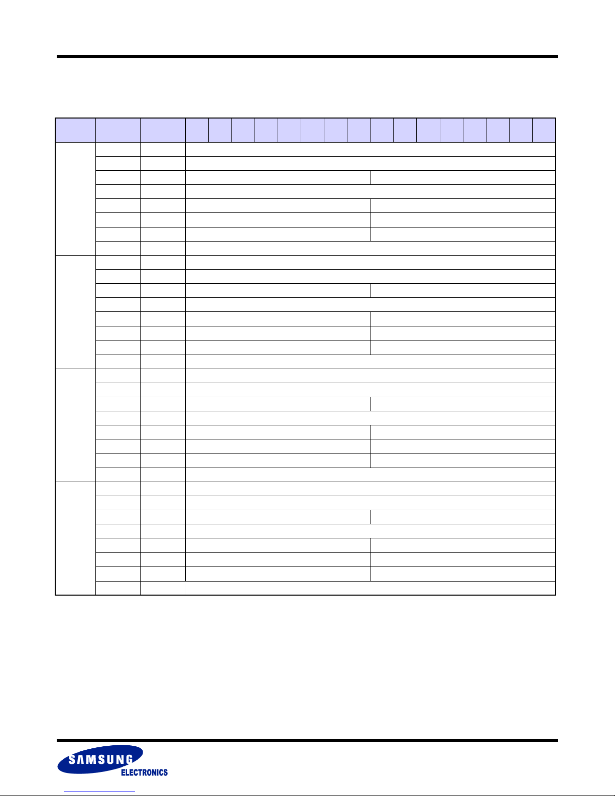
MuxOneNAND2G(KFM2G16Q2A-DEBx)
MuxOneNAND4G(KFN4G16Q2A-DEBx)
2.7.5 External Memory Spare Area Assignment
FLASH MEMORY
Buf.
BootS 0
BootS 1
DataS
0_0
DataS
0_1
Word
Address
Byte
Address
F E D C B A 9 8 7 6 5 4 3 2 1 0
8000h 10000h BI
8001h 10002h Managed by Internal ECC logic
8002h 10004h Reserved for the future use Managed by Internal ECC logic
8003h 10006h Reserved for the current and future use
8004h 10008h
8005h 1000Ah
ECC Code for Main area data (2
ECC Code for Spare area data (1
8006h 1000Ch FFh(Reserved for the future use)
nd
) ECC Code for Main area data (1st)
st
) ECC Code for Main area data (3rd)
ECC Code for Spare area data (2
8007h 1000Eh Free Usage
8008h 10010h BI
8009h 10012h Managed by Internal ECC logic
800Ah 10014h Reserved for the future use Managed by Internal ECC logic
800Bh 10016h Reserved for the current and future use
800Ch 10018h
800Dh 1001Ah
ECC Code for Main area data (2
ECC Code for Spare area data (1
800Eh 1001Ch FFh(Reserved for the future use)
nd
) ECC Code for Main area data (1st)
st
) ECC Code for Main area data (3rd)
ECC Code for Spare area data (2
800Fh 1001Eh Free Usage
8010h 10020h BI
8011h 10022h Managed by Internal ECC logic
8012h 10024h Reserved for the future use Managed by Internal ECC logic
8013h 10026h Reserved for the current and future use
8014h 10028h
8015h 1002Ah
ECC Code for Main area data (2
ECC Code for Spare area data (1
8016h 1002Ch FFh(Reserved for the future use)
nd
) ECC Code for Main area data (1st)
st
) ECC Code for Main area data (3rd)
ECC Code for Spare area data (2
8017h 1002Eh Free Usage
8018h 10030h BI
8019h 10032h Managed by Internal ECC logic
801Ah 10034h Reserved for the future use Managed by Internal ECC logic
801Bh 10036h Reserved for the current and future use
801Ch 10038h
801Dh 1003Ah
ECC Code for Main area data (2
ECC Code for Spare area data (1
801Eh 1003Ch FFh(Reserved for the future use)
nd
) ECC Code for Main area data (1st)
st
) ECC Code for Main area data (3rd)
ECC Code for Spare area data (2
801Fh 1003Eh Free Usage
nd
)
nd
)
nd
)
nd
)
- 51 -
Page 52

MuxOneNAND2G(KFM2G16Q2A-DEBx)
MuxOneNAND4G(KFN4G16Q2A-DEBx)
Buf.
DataS 0_2
DataS 0_3
DataS 1_0
DataS 1_1
DataS 1_2
Word
Address
8020h 10040h BI
8021h 10042h Managed by Internal ECC logic
8022h 10044h Reserved for the future use Managed by Internal ECC logic
8023h 10046h Reserved for the current and future use
8024h 10048h
8025h 1004Ah
8026h 1004Ch Reserved for the future use
8027h 1004Eh Free Usage
8028h 10050h BI
8029h 10052h Managed by Internal ECC logic
802Ah 10054h Reserved for the future use Managed by Internal ECC logic
802Bh 10056h Reserved for the current and future use
802Ch 10058h
802Dh 1005Ah
802Eh 1005Ch Reserved for the future use
802Fh 1005Eh Free Usage
8030h 10060h BI
8031h 10062h Managed by Internal ECC logic
8032h 10064h Reserved for the future use Managed by Internal ECC logic
8033h 10066h Reserved for the current and future use
8034h 10068h
8035h 1006Ah
8036h 1006Ch Reserved for the future use
8037h 1006Eh Free Usage
8038h 10070h BI
8039h 10072h Managed by Internal ECC logic
803Ah 10074h Reserved for the future use Managed by Internal ECC logic
803Bh 10076h Reserved for the current and future use
803Ch 10078h
803Dh 1007Ah
803Eh 1007Ch Reserved for the future use
803Fh 1007Eh Free Usage
8040h 10080h BI
8041h 10082h Managed by Internal ECC logic
8042h 10084h Reserved for the future use Managed by Internal ECC logic
8043h 10086h Reserved for the current and future use
8044h 10088h
8045h 1008Ah
8046h 1008Ch Reserved for the future use
8047h 1008Eh Free Usage
Byte
Address
F E D C B A 9 8 7 6 5 4 3 2 1
ECC Code for Main area data (2
ECC Code for Spare area data (1
ECC Code for Main area data (2
ECC Code for Spare area data (1
ECC Code for Main area data (2
ECC Code for Spare area data (1
ECC Code for Main area data (2
ECC Code for Spare area data (1
ECC Code for Main area data (2
ECC Code for Spare area data (1
Equivalent to 1word of NAND Flash
nd
) ECC Code for Main area data (1st)
st
) ECC Code for Main area data (3rd)
ECC Code for Spare area data (2
nd
) ECC Code for Main area data (1st)
st
) ECC Code for Main area data (3rd)
ECC Code for Spare area data (2
nd
) ECC Code for Main area data (1st)
st
) ECC Code for Main area data (3rd)
ECC Code for Spare area data (2
nd
) ECC Code for Main area data (1st)
st
) ECC Code for Main area data (3rd)
ECC Code for Spare area data (2
nd
) ECC Code for Main area data (1st)
st
) ECC Code for Main area data (3rd)
ECC Code for Spare area data (2
FLASH MEMORY
nd
)
nd
)
nd
)
nd
)
nd
)
- 52 -
Page 53

MuxOneNAND2G(KFM2G16Q2A-DEBx)
MuxOneNAND4G(KFN4G16Q2A-DEBx)
FLASH MEMORY
Buf.
Word
Address
Byte
Address
F E D C B A 9 8 7 6 5 4 3 2 1 0
8048h 10090h BI
8049h 10092h Managed by Internal ECC logic
804Ah 10094h Reserved for the future use Managed by Internal ECC logic
DataS 1_3
804Bh 10096h Reserved for the current and future use
804Ch 10098h
804Dh 1009Ah
ECC Code for Main area data (2
ECC Code for Spare area data (1
804Eh 1009Ch Reserved for the future use
nd
) ECC Code for Main area data (1st)
st
) ECC Code for Main area data (3rd)
ECC Code for Spare area data (2
804Fh 1009Eh Free Usage
NOTE :
- BI: Bad block Information
>Host can use complete spare area except BI and ECC code area. For example,
Host can write data to Spare area buffer except for the area controlled by ECC logic at program operation.
>In case of ‘with ECC’ mode, MuxOneNAND automatically generates ECC code for both main and spare data of memory during program operation,
but does not update ECC code to spare bufferRAM during load operation.
>When loading/programming spare area, spare area BufferRAM address(BSA) and BufferRAM sector count(BSC) is chosen via Start buffer register
as it is.
nd
)
- 53 -
Page 54
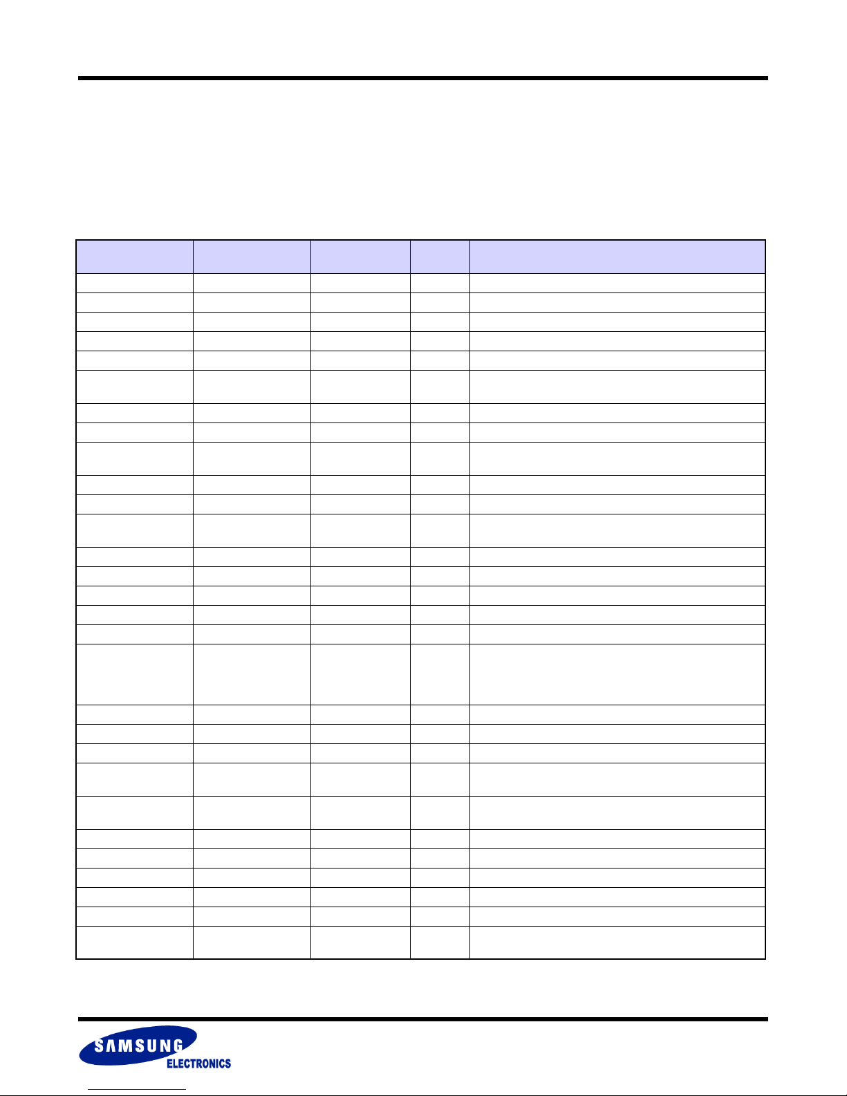
MuxOneNAND2G(KFM2G16Q2A-DEBx)
MuxOneNAND4G(KFN4G16Q2A-DEBx)
2.8 Registers
Section 2.8 of this specification provides information about the MuxOneNAND registers.
2.8.1 Register Address Map
This map describes the register addresses, register name, register description, and host accessibility.
FLASH MEMORY
Address
(word order)
F000h 1E000h Manufacturer ID R Manufacturer identification
F001h 1E002h Device ID R Device identification
F002h 1E004h Version ID R N/A
F003h 1E006h Data Buffer size R Data buffer size
F004h 1E008h Boot Buffer size R Boot buffer size
F005h 1E00Ah
F006h 1E00Ch Technology R Info about technology
F007h~F0FFh 1E00Eh~1E1FEh Reserved - Reserved for user
F100h 1E200h Start address 1 R/W
F101h 1E202h Start address 2 R/W Chip address for selection of BufferRAM in DDP
F102h 1E204h Start address 3 R/W Destination Block address for Copy back program
F103h 1E206h Start address 4 R/W
F104h 1E208h Start address 5 R/W Number of Page in Synchronous Burst Block Read
F105h 1E20Ah Start address 6 - N/A
F106h 1E20Ch Start address 7 - N/A
F107h 1E20Eh Start address 8 R/W NAND Flash Page & Sector address
F108h~F1FFh 1E210h~1E3FEh Reserved - Reserved for user
F200h 1E400h Start Buffer R/W
F201h~F207h 1E402h~1E40Eh Reserved - Reserved for user
F208h~F21Fh 1E410h~1E43Eh Reserved - Reserved for vendor specific purposes
F220h 1E440h Command R/W Host control and memory operation commands
F221h 1E442h
F222h 1E444h
F223h~F22Fh 1E446h~1E45Eh Reserved - Reserved for user
F230h~F23Fh 1E460h~1E47Eh Reserved - Reserved for vendor specific purposes
F240h 1E480h Controller Status R Controller Status and result of memory operation
F241h 1E482h Interrupt R/W Memory Command Completion Interrupt Status
F242h~F24Bh 1E484h~1E496h Reserved - Reserved for user
F24Ch 1E498h
Address
(byte order)
Name
Amount of
buffers
System
Configuration 1
System
Configuration 2
Start
Block Address
Host
Access
R Amount of data/boot buffers
Chip address for selection of NAND
Core in DDP & Block address
Destination Page & Sector address for Copy
back program
Buffer Number for the page data transfer to/from the memory and the start Buffer Address
The meaning is with which buffer to start and how many
buffers to use for the data transfer
R, R/W memory and Host Interface Configuration
-N/A
R/W Start memory block address in Write Protection mode
Description
- 54 -
Page 55
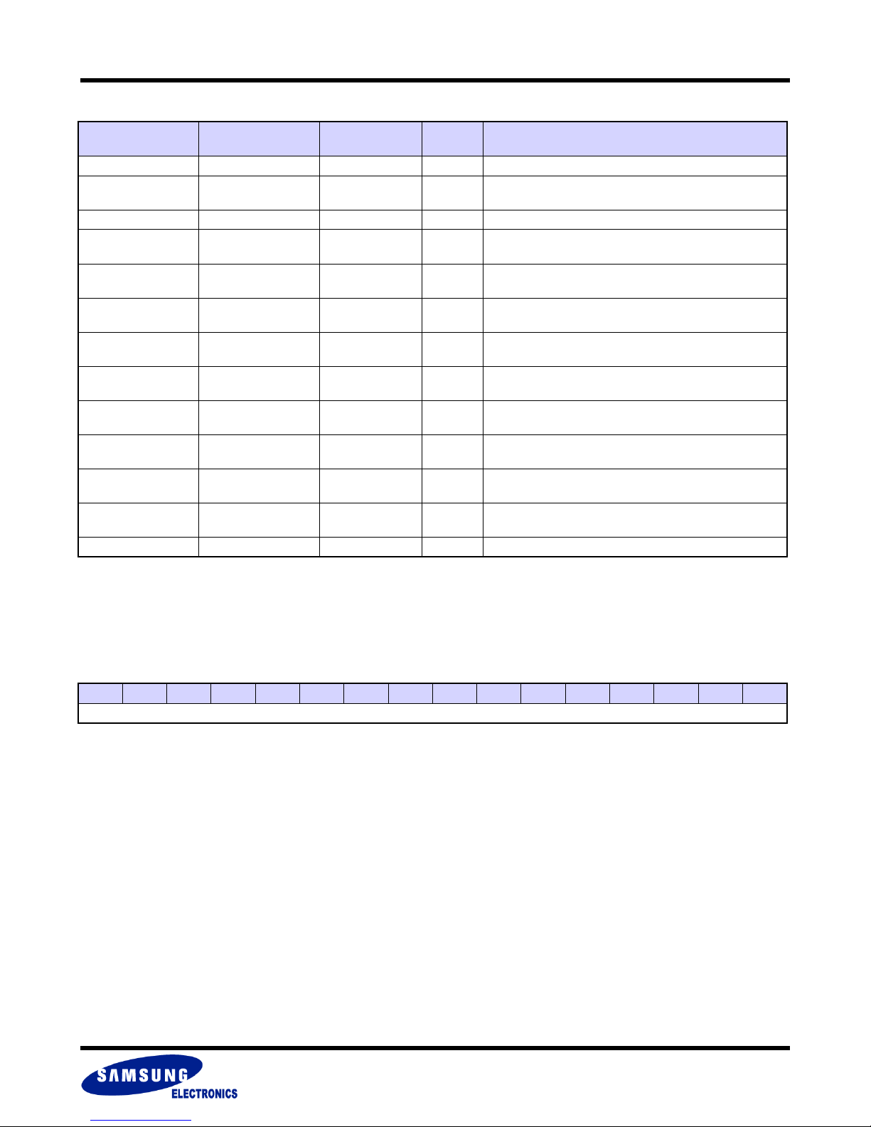
MuxOneNAND2G(KFM2G16Q2A-DEBx)
MuxOneNAND4G(KFN4G16Q2A-DEBx)
FLASH MEMORY
Address
(word order)
F24Dh 1E49Ah Reserved - Reserved for user
F24Eh 1E49Ch
F24Fh~FEFFh 1E49Eh~1FDFEh Reserved - Reserved for user
FF00h 1FE00h
FF01h 1FE02h
FF02h 1FE04h
FF03h 1FE06h
FF04h 1FE08h
FF05h 1FE0Ah
FF06h 1FE0Ch
FF07h 1FE0Eh
FF08h 1FE10h
FF09h~FFFFh 1FE12h~1FFFEh Reserved - Reserved for vendor specific purposes
Address
(byte order)
Name
Write Protection
Status
ECC Status
Register
ECC Result of
main area data
ECC Result of
spare area data
ECC Result of
main area data
ECC Result of
spare area data
ECC Result of
main area data
ECC Result of
spare area data
ECC Result of
main area data
ECC Result of
spare area data
Host
Access
Current memory Write Protection status
R
(unlocked/locked/tight-locked)
R ECC status of sector
ECC error position of Main area data error for first selected
R
Sector
ECC error position of Spare area data error for first
R
selected Sector
ECC error position of Main area data error for second
R
selected Sector
ECC error position of Spare area data error for second
R
selected Sector
ECC error position of Main area data error for third
R
selected Sector
ECC error position of Spare area data error for third
R
selected Sector
ECC error position of Main area data error for fourth
R
selected Sector
ECC error position of Spare area data error for fourth
R
selected Sector
Description
2.8.2 Manufacturer ID Register F000h (R)
This Read register describes the manufacturer's identification.
Samsung Electronics Company manufacturer's ID is 00ECh.
F000h, default = 00ECh
15 14 13 12 11 10 9 8 7 6 5 4 3 2 1 0
ManufID
- 55 -
Page 56
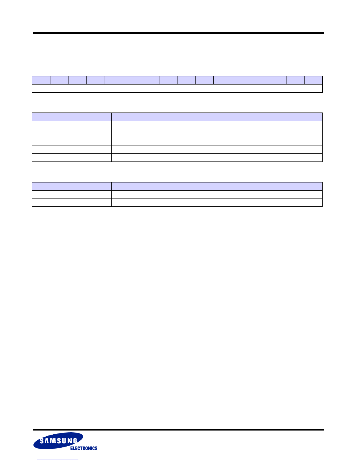
MuxOneNAND2G(KFM2G16Q2A-DEBx)
MuxOneNAND4G(KFN4G16Q2A-DEBx)
2.8.3 Device ID Register F001h (R)
This Read register describes the device.
F001h, see table for default.
15 14 13 12 11 10 9 8 7 6 5 4 3 2 1 0
DeviceID
Device Identification
Device Identification Description
DeviceID [1:0] Vcc 00 = 1.8V, 01/10/11 = reserved
DeviceID [2] Muxed/Demuxed 0 = Muxed, 1 = Demuxed
DeviceID [3] Single/DDP 0 = Single, 1 = DDP
DeviceID [7:4] Density 0000 = 128Mb, 0001 = 256Mb, 0010 = 512Mb, 0011 = 1Gb, 0100 = 2Gb, 0101=4Gb
DeviceID [8] Bottom Boot 0 = Bottom Boot
Device ID Default
Device DeviceID[15:0]
KFM2G16Q2A 0040h
KFN4G16Q2A 0058h
FLASH MEMORY
- 56 -
Page 57
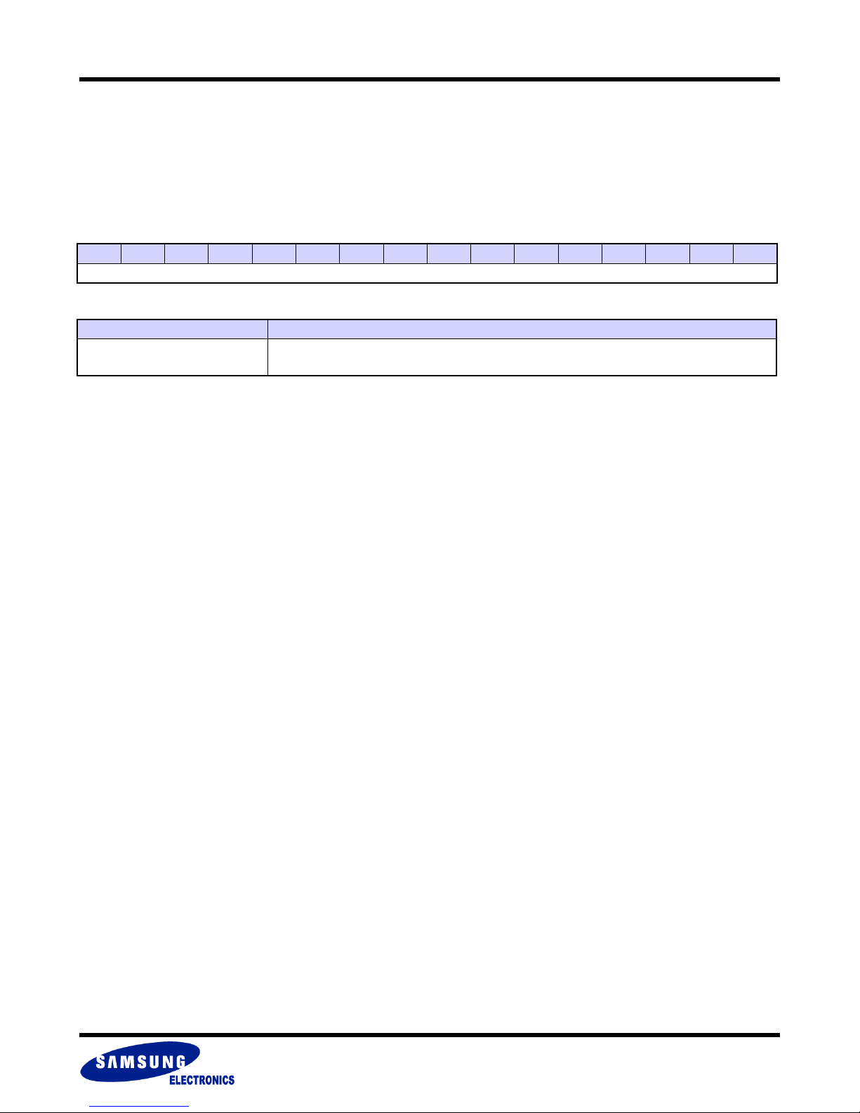
MuxOneNAND2G(KFM2G16Q2A-DEBx)
MuxOneNAND4G(KFN4G16Q2A-DEBx)
2.8.4 Version ID Register F002h
This Register is reserved for internal use.
2.8.5 Data Buffer Size Register F003h (R)
F003h, default = 0800h
15 14 13 12 11 10 9 8 7 6 5 4 3 2 1 0
DataBufSize
Data Buffer Size Information
Register Information Description
DataBufSize
Total data buffer size in Words equal to 2 buffers of 1024 Words each
(2 x 1024 = 2
11
) in the memory interface
FLASH MEMORY
- 57 -
Page 58
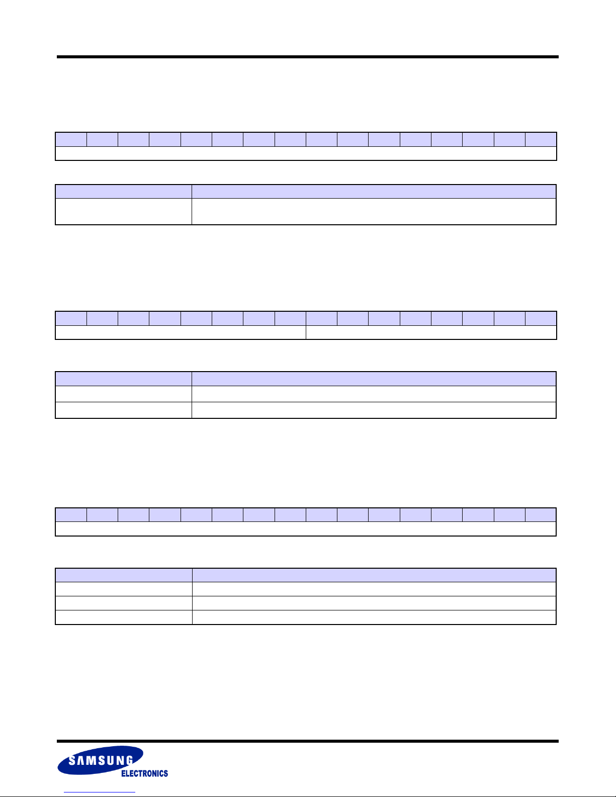
MuxOneNAND2G(KFM2G16Q2A-DEBx)
MuxOneNAND4G(KFN4G16Q2A-DEBx)
2.8.6 Boot Buffer Size Register F004h (R)
This Read register describes the size of the Boot Buffer.
F004h, default = 0200h
15 14 13 12 11 10 9 8 7 6 5 4 3 2 1 0
BootBufSize
Register Information Description
BootBufSize
2.8.7 Number of Buffers Register F005h (R)
This Read register describes the number of each Buffer.
F005h, default = 0201h
15 14 13 12 11 10 9 8 7 6 5 4 3 2 1 0
DataBufAmount BootBufAmount
Total boot buffer size in Words equal to 1 buffer of 512 Words
(1 x 512 = 2
9
) in the memory interface
FLASH MEMORY
Number of Buffers Information
Register Information Description
DataBufAmount
BootBufAmount
The number of data buffers = 2 (2
The number of boot buffers = 1 (2
N
, N=1)
N
, N=0)
2.8.8 Technology Register F006h (R)
This Read register describes the internal NAND array technology.
F006h, default = 0000h
15 14 13 12 11 10 9 8 7 6 5 4 3 2 1 0
Te ch
Technology Information
Technology Register Setting
NAND SLC 0000h
NAND MLC 0001h
Reserved 0002h ~ FFFFh
- 58 -
Page 59
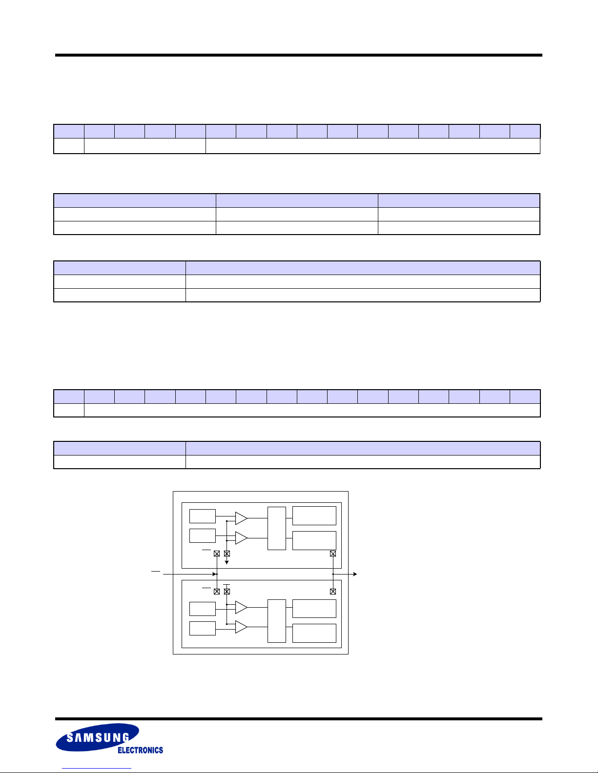
MuxOneNAND2G(KFM2G16Q2A-DEBx)
MuxOneNAND4G(KFN4G16Q2A-DEBx)
2.8.9 Start Address1 Register F100h (R/W)
This Read/Write register describes the NAND Flash block address which will be loaded, programmed, or erased.
F100h, default = 0000h
15 14 13 12 11 10 9 8 7 6 5 4 3 2 1 0
DFS Reserved(0000)
NOTE :
1) Bit 0 should be fixed ‘low’ at 2X Program and 2X Cache Program.
Device Number of Block FBA
2Gb 2048 FBA[10:0]
4Gb DDP 4096 DFS[15] & FBA[10:0]
Start Address1 Information
Register Information Description
FBA NAND Flash Block Address
DFS Flash Core of DDP (Device Flash Core Select)
FBA
1)
FLASH MEMORY
2.8.10 Start Address2 Register F101h (R/W)
This Read/Write register describes the BufferRAM of DDP (Device BufferRAM Select)
F101h, default = 0000h
15 14 13 12 11 10 9 8 7 6 5 4 3 2 1 0
DBS Reserved(000000000000000)
Start Address2 Information
Register Information Description
DBS BufferRAM and Register of DDP (Device BufferRAM Select)
CHIP 1
DBS
DFS
CE
CE INT
CE
DBS
DFS
Comp
Comp
DDP_OPT
GND
V
DD
DDP_OPT
Comp
Comp
CHIP 2
CONTROL
CONTROL
LOGIC
LOGIC
SRAM
BUFFER
FLASH
CORE
INT
INT
SRAM
BUFFER
FLASH
CORE
*Comp = Comparator
In the case of writing Register, both registers in chip1 and chip2 will be written regardless of DBS. Reading out from Register of chip1/chip2
follows the DBS setting.
In using DDP chip, BootRAM of Chip 1 will always be selected regardless of DBS.
Reading and Writing on the DataRAM of DDP chip is different. Only the DataRAM selected by DBS will be written and read out.
- 59 -
Page 60
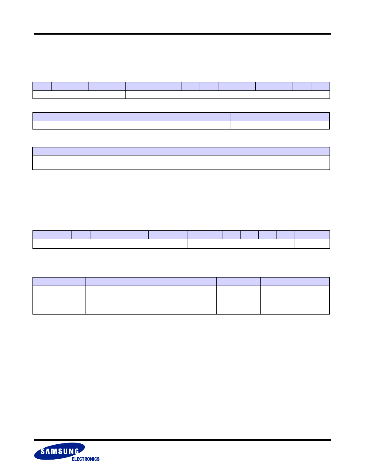
MuxOneNAND2G(KFM2G16Q2A-DEBx)
MuxOneNAND4G(KFN4G16Q2A-DEBx)
2.8.11 Start Address3 Register F102h (R/W)
This Read/Write register describes the NAND Flash destination block address which will be copy back programmed. Also, this register indicates the block address for the first page to be read in Cache Read Operation.
F102h, default = 0000h
15 14 13 12 11 10 9 8 7 6 5 4 3 2 1 0
Reserved(00000) FCBA
Device Number of Block FBA
2Gb 2048 FCBA[10:0]
Start Address3 Information
Register Information Description
FCBA
Block Address for the first page to be read in Cache Read Operation
2.8.12 Start Address4 Register F103h (R/W)
NAND Flash Copy Back Block Address &
FLASH MEMORY
This Read/Write register describes the NAND Flash destination page address in a block and the NAND Flash destination sector address in a
page for copy back programming. Also, this register describes the first page and sector address to be loaded in Cache Read Operation.
F103h, default = 0000h
15 14 13 12 11 10 9 8 7 6 5 4 3 2 1 0
Reserved(00000000) FCPA
NOTE :
1) In case of ‘Cache Read Operation’, FCSA has to be set to 00.
Start Address4 Information
Item Description Default Value Range
FCPA
FCSA
NAND Flash Copy Back Page Address &
First Page Address of Cache Read
NAND Flash Copy Back Sector Address &
First Sector Address of Cache Read
000000
00
000000 ~ 111111,
6 bits for 64 pages
00 ~ 11,
2 bits for 4 sectors
FCSA
1)
- 60 -
Page 61
MuxOneNAND2G(KFM2G16Q2A-DEBx)
MuxOneNAND4G(KFN4G16Q2A-DEBx)
2.8.13 Start Address5 Register F104h (R/W)
This Read/Write register describes the number of page in Synchronous Burst Block Read.
F104h, default = 0000h
15 14 13 12 11 10 9 8 7 6 5 4 3 2 1 0
Reserved(0000000000) FPC
Flash Page Count (FPC) Information
FPC Number of Page
000000 (Default) 64 page
000011 3 page
000100 4 page
.. ..
111111 63 pa g e
NOTE :
Synchronous Burst Block Read are NOT able to be perforformed with 1 or 2pages.
2.8.14 Start Address6 Register F105h
FLASH MEMORY
This register is reserved for future use.
2.8.15 Start Address7 Register F106h
This register is reserved for future use.
2.8.16 Start Address8 Register F107h (R/W)
This Read/Write register describes the NAND Flash start page address in a block for a page load, copy back program, or program operation
and the NAND Flash start sector address in a page for a load, copy back program, or program operation.
F107h, default = 0000h
15 14 13 12 11 10 9 8 7 6 5 4 3 2 1 0
Reserved (00000000)
NOTE :
1) In case of ‘2X Cache Program’, the host programs data on same FPA of different Planes.
2) In case of ‘ Synchronous Burst Block Read’, ‘Cache Read Operation’, ‘2X Program’ and ‘2X Cache Program’,
FSA has to be set to 00.
Start Address8 Information
Item Description Default Value Range
FPA NAND Flash Page Address 000000
FSA NAND Flash Sector Address 00
FPA
1)
000000 ~ 111111,
6 bits for 64 pages
00 ~ 11,
2 bits for 4 sectors
FSA
2)
- 61 -
Page 62
MuxOneNAND2G(KFM2G16Q2A-DEBx)
MuxOneNAND4G(KFN4G16Q2A-DEBx)
2.8.17 Start Buffer Register F200h (R/W)
This Read/Write register describes the BufferRAM Sector Count (BSC) and BufferRAM Sector Address (BSA).
The BufferRAM Sector Count (BSC) field specifies the number of sectors to be loaded, programmed, or copy back programmed. At 00 value
(the default value), the number of sector is "4". If the internal RAM buffer reaches its maximum value of 11, it will count up to 0 value to meet
the BSC value. For example, if BSA = 1101, BSC = 00, then the selected BufferRAM will count up from '1101
The BufferRAM Sector Address (BSA) is the sector 0~3 address in the internal BootRAM and DataRAM where data is placed.
F200h, default = 0000h
15 14 13 12 11 10 9 8 7 6 5 4 3 2 1 0
Reserved(0000) BSA Reserved(000000) BSC
NOTE :
In case of ’Cache Read’, BSA has to be set to 1000 or 1100. And BSC has to be set to 00.
In case of ’Synchronous Burst Block Read’, BSA has to be set to 1000 . And BSC has to be set to 00.
In case of ’2X Program’ or ’2X Cache Program’, BSA has to be set to 1000. And BSC has to be set to 00.
Start Address8 Information
Item Description
BSA[3] Selection bit between BootRAM and DataRAM
BSA[2] Selection bit between DataRAM0 and DataRAM1
BSA[1:0]
Selection bit between Sector0 and Sector1 in the internal BootRAM
Selection bit between Sector0 to Sector3 in the internal DataRAM
FLASH MEMORY
1110 1111 1100'.
Main area data
512B
BootRAM 0
BootRAM
DataRAM0
DataRAM1
BSC Number of Sectors
01 1 sector
10 2 sector
11 3 s e c t or
00 4 sector
BootRAM 1
DataRAM 0_0
DataRAM 0_1
DataRAM 0_2
DataRAM 0_3
DataRAM 1_0
DataRAM 1_1
DataRAM 1_2
DataRAM 1_3
Spare area data
16B
BSA
0000
0001
1000
1001
1010
1011
1100
1101
1110
1111
Sector: (512 + 16) Byte
- 62 -
Page 63
MuxOneNAND2G(KFM2G16Q2A-DEBx)
MuxOneNAND4G(KFN4G16Q2A-DEBx)
2.8.18 Command Register F220h (R/W)
Command can be issued by two following methods, and user may select one way or the other to issue appropriate command;
1. Write command into Command Register when INT is at ready state. INT will automatically turn to busy state as command is issued. Once
the desired operation is completed, INT will go back ready state.
2. Write 0000h to INT bit of Interrupt Status Register, and then write command into Command Register. Once the desired operation is completed, INT will go back to ready state.
(00F0h and 00F3h may be accepted during busy state of some operations. Refer to the rightmost column of the command register table
below.)
F220h, default = 0000h
15 14 13 12 11 10 9 8 7 6 5 4 3 2 1 0
Command
CMD Operation
0000h Load single/multiple sector data unit into buffer 00F0h, 00F3h
0013h Load single/multiple spare sector into buffer 00F0h, 00F3h
0080h
001Ah Program single/multiple spare data unit from buffer 00F0h, 00F3h
001Bh Copy back Program operation 00F0h, 00F3h
007Dh
007Fh
0023h Unlock NAND array a block 00F0h, 00F3h
002Ah Lock NAND array a block 00F0h, 00F3h
002Ch Lock-tight NAND array a block 00F0h, 00F3h
0027h
0071h Erase Verify Read 00F0h, 00F3h
000Eh Cache Read 00F0h, 00F3h
000Ch Finish Cache Read 00F0h, 00F3h
000Ah Synchronous Burst Block Read 00F0h, 00F3h
0094h Block Erase 00F0h, 00F3h
0095h Multi-Block Erase 00F0h, 00F3h
00B0h Erase Suspend 00F0h, 00F3h
0030h Erase Resume 00F0h, 00F3h
00F0h Reset NAND Flash Core -
00F3h
0065h OTP Access 00F0h, 00F3h
NOTE :
1) 0080h programs both main and spare area, while 001Ah programs only spare area. Refer to chapter 5.9 for NOP limits in issuing these commands. When using
0080h and 001Ah command, Read-only part in spare area must be masked by FF. (Refer to chapter 2.7.2)
2) ‘2X Program’ is executed by ‘007D’. This command can be used alone and used for ending ‘2X Cache Program’.
’2X Cache Program’ is executed by ‘007F’. This command cannot be used alone and must be ended by ‘007D’ for the last page program of cache program.
(Refer to 6.13 and 6.14)
3) If any blocks are changed to locked-tight state, the all block unlock command will fail. In order to use all block unlock command again, a cold reset is needed.
4) ‘Reset MuxOneNAND’(=Hot reset) command makes the registers and NAND Flash core into default state.
Program single/multiple sector data unit from buffer
2X Program operation
2X Cache Program operation
All Block Unlock
Reset MuxOneNAND
2)
2)
3)
4)
1)
FLASH MEMORY
Acceptable
command
during busy
00F0h, 00F3h
00F0h, 00F3h
00F0h, 00F3h
00F0h, 00F3h
-
- 63 -
Page 64
MuxOneNAND2G(KFM2G16Q2A-DEBx)
MuxOneNAND4G(KFN4G16Q2A-DEBx)
2.8.18.1 Two Methods to Clear Interrupt Register in Command Input
FLASH MEMORY
To clear Interrupt Register in command input, user may select one from either following methods.
First method is to turn INT low by manually writing 0000h to INT bit of Interrupt Register.
Second method is input command while INT is high, and the device will automatically turn INT to low.
(Second method is equivalent with method used in general NAND Flash)
User may choose the desirable method to clear Interrupt Register.
Method 1: Manually set INT=0 before writing command into Command Register: Manual INT Mode
(1) Clear Interrupt Register (F241h) by writing 0000h into INT bit of Interrupt Register. This operation will make INT pin turn low.
(2) Write command into Command Register. This will make the device to perform the designated operation.
(3) INT pin will turn back to high once the operation is completed.
INT pin1)
INT bit
Write 0 into
INT bit of
Interrupt Register
NOTE : 1) INT pin polarity is based on ‘IOBE=1 and INT pol=1 (default)’ setting
Write command into
Command Register
1)
1)
1)
INT will automatically turn to high
when designated operation is completed.
1)
Method 2: Write command into Command Register at INT ready state: Auto INT Mode
(1) Write command into Command Register. This will automatically turn INT from high to low.
(2) INT pin will turn back to high once the operation is completed.
INT pin1)
INT bit
Write command into
Command Register
NOTE : 1) INT pin polarity is based on ‘IOBE=1 and INT pol=1 (default)’ setting
INT will automatically
turn to Busy State
1)
INT will automatically turn back to ready state
when designated operation is completed.
1)
- 64 -
Page 65
MuxOneNAND2G(KFM2G16Q2A-DEBx)
MuxOneNAND4G(KFN4G16Q2A-DEBx)
2.8.19 System Configuration 1 Register F221h (R, R/W)
This Read/Write register describes the system configuration.
F221h, default = 40C0h
15 14 13 12 11 10 9 8 7 6 5 4 3 2 1 0
R/W R/W R/W R/W R/W R/W R/W R/W R R/W R/W R
RM BRWL BL ECC
Read Mode (RM)
RM Read Mode
0 Asynchronous read(default)
1 Synchronous read
Read Mode Information[15]
Item Definition Description
RM Read Mode
RDY
pol
INT
pol
IOBE
RDY
Conf
Selects between asynchronous read mode and
FLASH MEMORY
Reserv
synchronous read mode
HF WM BWPS
ed
Burst Read Write Latency (BRWL)
Latency Cycles (Read/Write)
BRWL
000~010 Reserved
011 3(up to 40MHz. min) 3(N/A) 3(N/A)
100 (default) 4 4(min.) 4(N/A)
101 5 5 5(N/A)
110 6 6 6( min .)
111 777
* Default value of BRWL and HF value is BRWL=4, HF=0.
For host frequency over 66MHz, BRWL should be 6 or 7 while HF is 1.
For host frequency range of 40MHz~66MHz, BRWL should be set to 4~7 while HF is 0.
For host frequency under 40MHz, BRWL should be set to 3~7 while HF is 0.
Burst Read Write Latency (BRWL) Information[14:12]
Item Definition Description
BRWL
under 40MHz
(HF=0)
Burst Read Latency /
Burst Write Latency
40MHz~66MHz
(HF=0)
over 66MHz
(HF=1)
Specifies the access latency in the burst
read / write transfer for the initial access
- 65 -
Page 66
MuxOneNAND2G(KFM2G16Q2A-DEBx)
MuxOneNAND4G(KFN4G16Q2A-DEBx)
Burst Length (BL)
Hosts must follow burst length set by BL when reading data in synchronous burst read.
BL Burst Length(Main) Burst Length(Spare)
000 Continuous(default)
001 4 words
010 8 words
011 16 words
100 32 words N/A
101 1K words (Block Read Only) N/A
110~111 Reserved
NOTE :
1) For normal synchronous burst read, setting BL=000 (continuous) will read 1K words, depending on the number of clocks. In using Synchronous Burst Block
Read, setting BL=000 (continuous) will read the amount of data in a block set by number of page register.
2) Even in using Synchronous Burst Block Read, it is possible to use above burst length by setting BL register by following the above table.
Burst Length (BL) Information[11:9]
Item Definition Description
Specifies the size of the burst length during a synchronous
BL Burst Length
linear burst read and wrap around. And also burst length during a
synchronous linear burst write
FLASH MEMORY
Error Correction Code (ECC) Information[8]
Item Definition Description
ECC Error Correction Code Operation
RDY Polarity (RDYpol) Information[7]
Item Definition Description
RDYpol RDY signal polarity
INT Polarity (INTpol) Information[6]
INTpol INT bit of Interrupt Status Register INT Pin output
0
1 (default)
0 = with correction (default)
1 = without correction (bypassed)
1 = high for ready (default)
0 = low for ready
0 (busy) High
1 (ready) Low
0 (busy) Low
1 (ready) High
- 66 -
Page 67
MuxOneNAND2G(KFM2G16Q2A-DEBx)
MuxOneNAND4G(KFN4G16Q2A-DEBx)
I/O Buffer Enable (IOBE)
IOBE is the I/O Buffer Enable for the INT and RDY signals. At startup, INT and RDY outputs are High-Z. Bits 6 and 7 become valid after IOBE
is set to "1". IOBE can be reset by a Cold Reset or by writing "0" to bit 5 of System Configuration1 Register.
I/O Buffer Enable Information[5]
Item Definition Description
IOBE
RDY Configuration (RDY conf)
RDY Configuration Information[4]
Item Definition Description
RDY conf RDY configuration
HF Enable (HF)
HF Description
0 HF Disable (default, 66Mhz and under)
1 HF Enable (over 66MHz)
I/O Buffer Enable for INT and
RDY signals
0=active with valid data(default)
1=active one clock before valid data
FLASH MEMORY
0 = disable (default)
1 = enable
HF Information[2]
Item Definition Description
HF High Frequency
Selects between HF Disable and
HF Enable
- 67 -
Page 68
MuxOneNAND2G(KFM2G16Q2A-DEBx)
MuxOneNAND4G(KFN4G16Q2A-DEBx)
Write Mode (WM)
WM Write Mode
0 Asynchronous Write(default)
1 Synchronous Write
Write Mode Information[1]
Item Definition Description
WM Write Mode
MRS(Mode register Setting) Description
RM WM Mode Description
0 0 Asynch Read & Asynch Write (Default)
1 0 Sync Read & Asynch Write
1 1 Sync Read & Synch Write
Other Case
NOTE :
1) Operation not guaranteed for cases not defined in above table.
Reserved
FLASH MEMORY
Selects between asynchronous Write Mode and
synchronous Write Mode
1)
Boot Buffer Write Protect Status(BWPS)
Boot Buffer Write Protect Status Information[0]
Item Definition Description
BWPS Boot Buffer Write Protect Status 0=locked(fixed)
- 68 -
Page 69
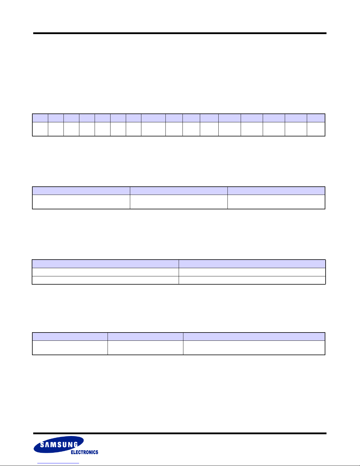
MuxOneNAND2G(KFM2G16Q2A-DEBx)
MuxOneNAND4G(KFN4G16Q2A-DEBx)
2.8.20 System Configuration 2 Register F222h
This register is reserved for future use.
2.8.21 Controller Status Register F240h (R)
This Read register shows the overall internal status of the MuxOneNAND and the controller.
F240h, default = 0000h
15 14 13 12 11 10 9 8 7 6 5 4 3 2 1 0
BL
Plane1
Previous
OTP
OnGo Lock Load Prog Erase Error Sus Reserved RSTB OTP
OnGo
This bit shows the overall internal status of the MuxOneNAND device.
In 2X Cache Program Operation, OnGo bit shows the overall status of 2X Cache Program process.
OnGo Information[15]
Item Definition Description
OnGo Internal Device Status
L
Plane1
Current
FLASH MEMORY
Plane2
Previous
0 = ready
1 = busy
Plane2
CurrentTO(0)
Lock
This bit shows whether the host is loading data from the NAND Flash array into the locked BootRAM or whether the host is performing a program/erase of a locked block of the NAND Flash array.
Lock Information[14]
Lock Locked/Unlocked Check Result
0 Unlocked
1 Locked
Load
This bit shows the Load Operation status.
Load Information[13]
Item Definition Description
Load Load Operation status
1 = busy or error (see controller status output modes)
0 = ready (default)
- 69 -
Page 70
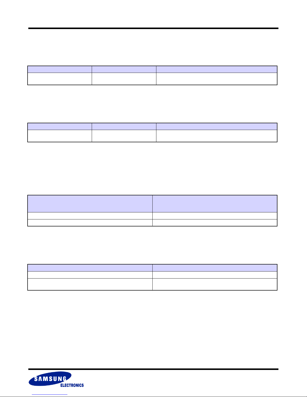
MuxOneNAND2G(KFM2G16Q2A-DEBx)
MuxOneNAND4G(KFN4G16Q2A-DEBx)
Program
This bit shows the Program Operation status.
In 2X Cache Program Operation, ‘Prog’ bit shows the overall status of 2X Cache Program process.
Program Information[12]
Item Definition Description
Prog Program Operation status
Erase
This bit shows the Erase Operation status.
Erase Information[11]
Item Definition Description
Erase Erase Operation status
Error
1 = busy or error (see controller status output modes)
1 = busy or error (see controller status output modes)
FLASH MEMORY
0 = ready (default)
0 = ready (default)
This bit shows the overall Error status, including Load Reset, Program Reset, and Erase Reset status.
In case of 2X Cache Program, Error bit will show the accumulative error status of 2X Cache Program operation, so that if an error occurs during 2X Cache Program, this bit will stay as Fail status, until the end of 2X Cache Program.
In case of 2X Program, Error bit will indicate the 2X Program fail, regardless of Plane1 or Plane2.
Error Information[10]
Sector/Page Load/Program/CopyBack,
Error
0Pass
1Fail
Erase Suspend (Sus)
This bit shows the Erase Suspend status.
Sus Information[9]
Sus Erase Suspend Status
0 Erase Resume(Default)
1
Program/2X Program/2X Cache Program Result
and Invalid Command Input
Erase Suspend, Program Ongoing(Susp.), Load Ongoing(Susp.),
Program Fail(Susp.), Load Fail(Susp.), Invalid Command(Susp.)
- 70 -
Page 71
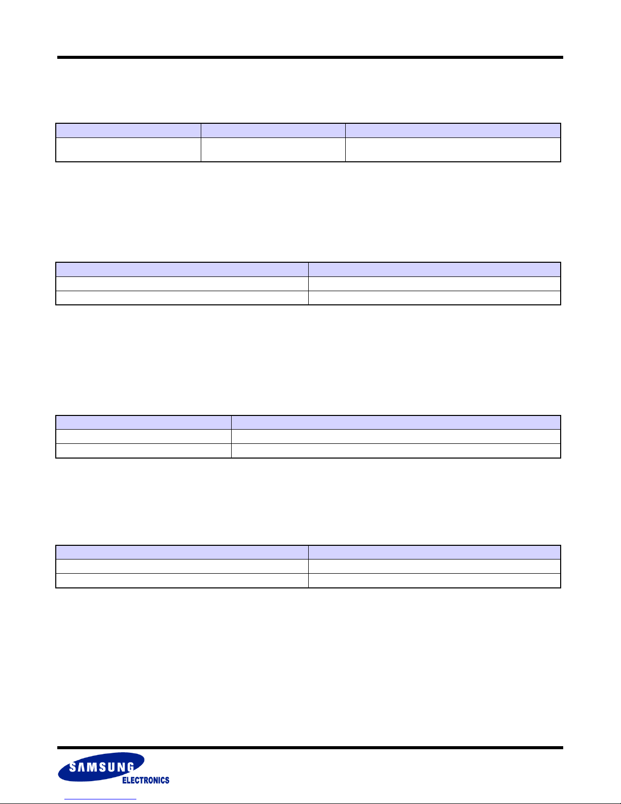
MuxOneNAND2G(KFM2G16Q2A-DEBx)
MuxOneNAND4G(KFN4G16Q2A-DEBx)
Reset / Busy (RSTB)
This bit shows the Reset Operation status.
RSTB Information[7]
Item Definition Description
RSTB Reset Operation Status
FLASH MEMORY
0 = ready (default)
1 = busy (see controller status output modes)
OTP Lock Status (OTP
This bit shows whether the OTP block is locked or unlocked. Locking the OTP has the effect of a 'write-protect' to guard against accidental reprogramming of data stored in the OTP block.
The OTP
OTP Lock Information[6]
1st Block OTP Lock Status (OTP
This bit shows whether the 1st Block OTP is locked or unlocked.
Locking the 1st Block OTP has the effect of a 'Program/Erase protect' to guard against accidental re-programming of data stored in the 1st
block.
The OTP
OTP Lock Information[5]
status bit is automatically updated at power-on and it must be referred only on Chip1 within DDP.
L
status bit is automatically updated at power-on and it must be referred only on Chip1 within DDP.
BL
)
L
OTPL OTP Locked/Unlocked Status
0 OTP Block Unlock Status(Default)
1 OTP Block Lock Status(Disable OTP Program/Erase)
)
BL
OTPBL 1st Block OTP Locked/Unlocked Status
0 1st Block OTP Unlock Status(Default)
1 1st Block OTPLock Status(Disable 1st Block OTP Program/Erase)
Plane1 Previous
This bit shows the previous program status of Plane1 at 2X Cache Program. This value is invalid only at the first ‘Read Controller Status Register’ step of 2X Cache Program and 2X Interleave Cache Program operation. (Refer to 6.14 and 6.15)
Plane1 Previous Information[4]
Plane1 Previous Status of previous program on Plane1
0Pass
1Fail
- 71 -
Page 72
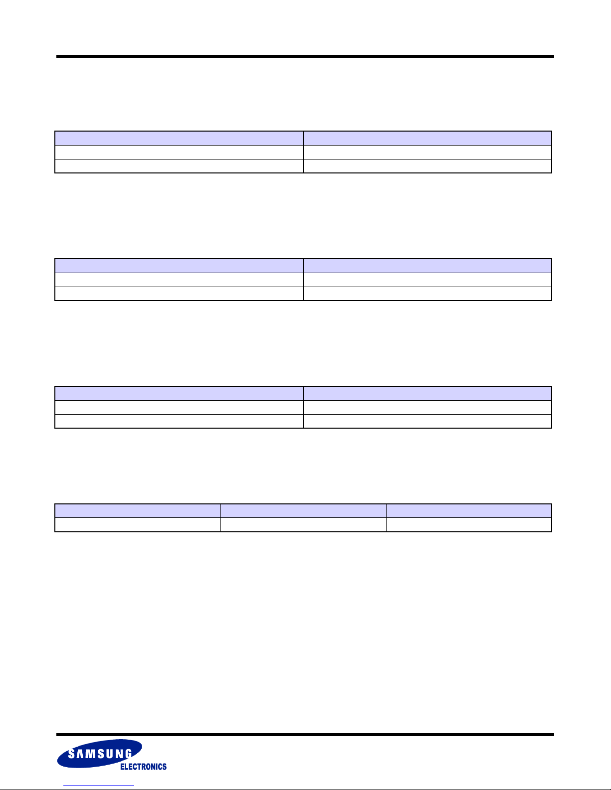
MuxOneNAND2G(KFM2G16Q2A-DEBx)
MuxOneNAND4G(KFN4G16Q2A-DEBx)
Plane1 Current
This bit shows the current program status of Plane1 at Final 2X Cache Program, 2X Program, and 2X Interleave Cache Program.
During 2X Cache Program prior to ‘2X Program’ command, which will be Final 2X Cache Program, this bit will be invalid (fixed to 0).
Plane1 Current Information[3]
Plane1 Current Status of current program on Plane1
0Pass
1Fail
Plane2 Previous
This bit shows the previous program status of Plane2 at 2X Cache Program. This value is invalid only at the first ‘Read Controller Status Register’ step of 2X Cache Program and 2X Interleave Cache Program operation. (Refer to 6.14 and 6.15)
Plane2 Previous Information[2]
Plane2 Previous Status of previous program on Plane2
0Pass
1Fail
FLASH MEMORY
Plane2 Current
This bit shows the current program status of Plane2 at Final 2X Cache Program, 2X Program, and 2X Interleave Cache Program.
During 2X Cache Program prior to ‘2X Program’ command, which will be Final 2X Cache Program, this bit will be invalid (fixed to 0).
Plane2 Current Information[1]
Plane2 Current Status of current program on Plane2
0Pass
1Fail
Time Out (TO)
This bit determines if there is a time out for load, program, copy back program, and erase operations. It is fixed at 'no time out'.
TO Information[0]
Item Definition Description
TO Time Out 0 = no time out
- 72 -
Page 73
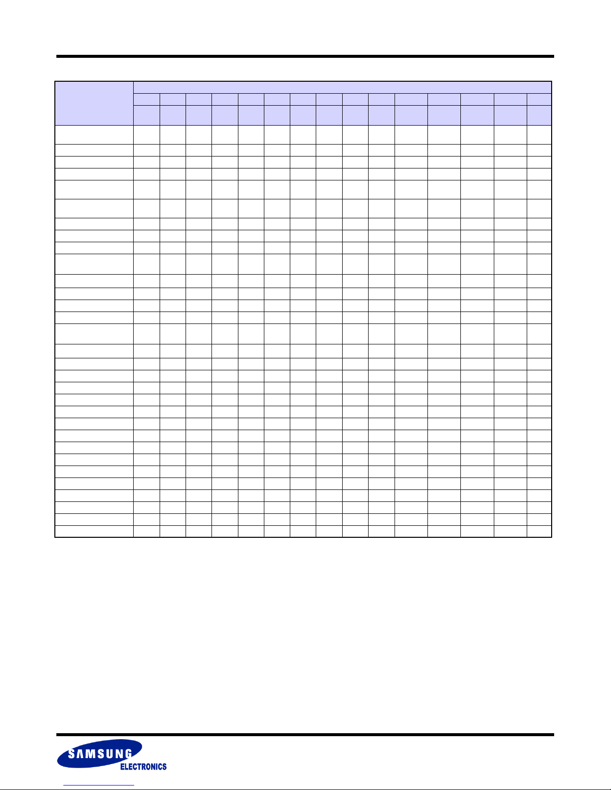
MuxOneNAND2G(KFM2G16Q2A-DEBx)
MuxOneNAND4G(KFN4G16Q2A-DEBx)
Controller Status Register Output Modes
Controller Status Register [15:0]
Mode
Load / Cache Read
Ongoing
Program Ongoing 100100000/10/1 0 0 0 0 0
Erase Ongoing 100010000/10/1 0 0 0 0 0
Reset Ongoing 100000010/10/1 0 0 0 0 0
Multi-Block Erase
Ongoing
Erase Verify Read
Ongoing
Load / Cache Read OK000000000/10/1 0 0 0 0 0
Program OK 000000000/10/1 0 0 0 0 0
Erase OK 000000000/10/1 0 0 0 0 0
Erase Verify Read
3)
OK
1)
Load Fail
Program Fail 000101000/10/1 0 0 0 0 0
Erase Fail 000011000/10/1 0 0 0 0 0
Cache Read Fail 101001000/10/1 0 0 0 0 0
Erase Verify Read
3)
Fail
Load Reset
Program Reset 000101010/10/1 0 0 0 0 0
Erase Reset 000011010/10/1 0 0 0 0 0
Erase Suspend 000010100/10/1 0 0 0 0 0
Program Lock 010101000/10/1 0 0 0 0 0
Load Lock(Buffer Lock)011001000/10/1 0 0 0 0 0
OTP Program Fail(Lock)0101010011 0 0 0 0 0
OTP Program Fail 0001010000 0 0 0 0 0
OTP Erase Fail 010011000/10/1 0 0 0 0 0
Program Ongoing(Susp.)100110100/10/1 0 0 0 0 0
Load Ongoing(Susp.)101010100/10/1 0 0 0 0 0
Program Fail(Susp.)000111100/10/1 0 0 0 0 0
Load Fail(Susp.) 001011100/10/1 0 0 0 0 0
Invalid Command 000001000/10/1 0 0 0 0 0
Invalid Command(Susp.)000011100/10/1 0 0 0 0 0
2)
Erase Lock 010011000/10/1 0 0 0 0 0
NOTE :
1) ERm and/or ERs bits in ECC status register at Load Fail case is 10. (2bits error - uncorrectable)
2) ERm and ERs bits in ECC status register at Load Reset case are 00. (No error)
3) Multi Block Erase status should be checked by Erase Verify Read operation.
4) "1" for OTP Block Lock, "0" for OTP Block Unlock.
5) "1" for 1st Block OTP Lock, "0" for 1st Block OTP Unlock.
[15] [14] [13] [12] [11] [10] [9] [7] [6] [5] [4] [3] [2] [1] [0]
OTP
OTP
OnGo Lock Load Prog Erase Error Sus RSTB
101000000/10/1 0 0 0 0 0
100010000/10/1 0 0 0 0 0
100000000/10/1 0 0 0 0 0
000000000/10/1 0 0 0 0 0
001001000/10/1 0 0 0 0 0
000011000/10/1 0 0 0 0 0
001001010/10/1 0 0 0 0 0
(note4)
L
(note5)
BL
Plane1
Previous
FLASH MEMORY
Plane1
Current
Plane2
Previous
Plane2
Current
TO
- 73 -
Page 74
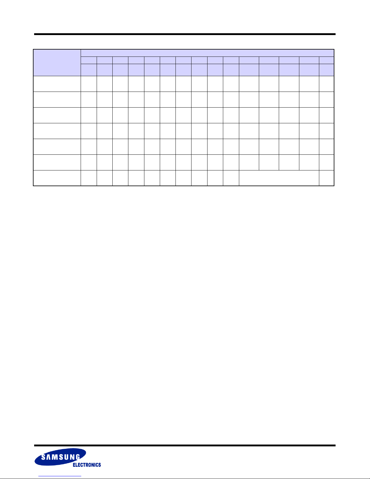
MuxOneNAND2G(KFM2G16Q2A-DEBx)
MuxOneNAND4G(KFN4G16Q2A-DEBx)
Controller Status Register Output Modes (Continued)
Controller Status Register [15:0]
Mode
Program Fail on
2X Program
(Plane1)
Program Fail on
2X Program
(Plane2)
Program Fail on
2X Program
(Plane1 & Plane2)
Previous Program Fail Dur-
ing 2X Cache Program
(Plane1)
Previous Program Fail Dur-
ing 2X Cache Program
(Plane2)
Previous Program Fail Dur-
ing 2X Cache Program
(Plane1 & Plane2)
Program Fail
After Final 2X
Cache Program
NOTE :
1) "1" for OTP Block Lock, "0" for OTP Block Unlock.
2) "1" for 1st Block OTP Lock, "0" for 1st Block OTP Unlock.
3) This value is invalid in this case. Host can recognize the status of the only previous operation.
4) Plane previous value is updated immediately after INT goes to ready state.4
After Final 2X Cache Program operation by ‘2X Program Command’ is completed, Current and Previous Program pass/fail status on both Plane1 and Plane2 will
be updated.
[15] [14] [13] [12] [11] [10] [9] [7] [6] [5] [4] [3] [2] [1] [0]
OTP
OTP
OnGo Lock Load Prog Erase Error Sus RSTB
000101000/10/1 0 1 0 0 0
000101000/10/1 0 0 0 1 0
000101000/10/1 0 1 0 1 0
100101000/10/1 1(Note3)0 0 0
100101000/10/1 0 0 1(Note3)0
100101000/10/1 1(Note3)1(Note3)0
000101000/10/1 (Note4) 0
(note1)
L
(note2)
BL
Plane1
Previous
FLASH MEMORY
Plane1
Current
Plane2
Previous
Plane2
Current
TO
- 74 -
Page 75
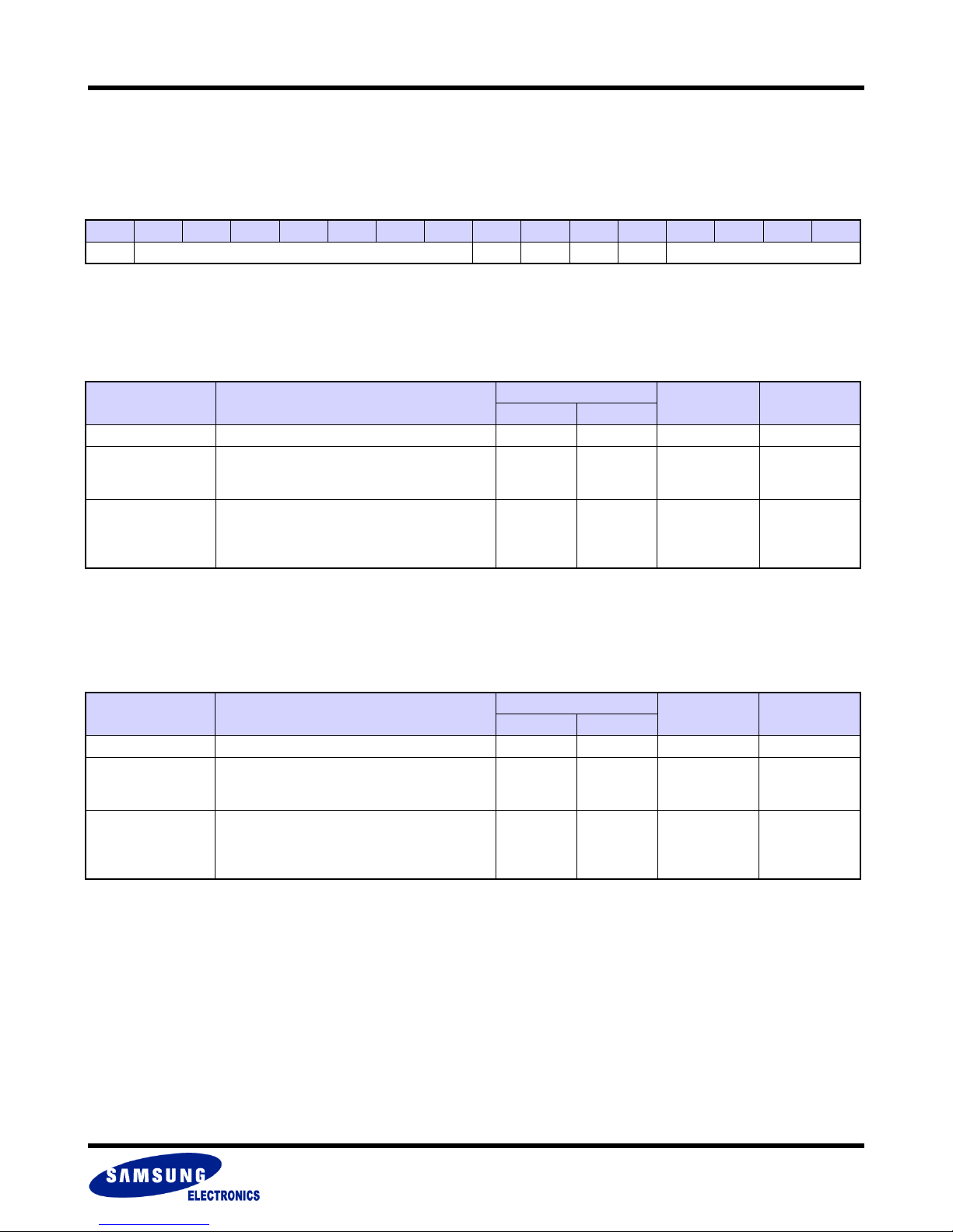
MuxOneNAND2G(KFM2G16Q2A-DEBx)
MuxOneNAND4G(KFN4G16Q2A-DEBx)
2.8.22 Interrupt Status Register F241h (R/W)
This Read/Write register shows status of the MuxOneNAND interrupts.
In DDP, INT register will not be written if DBS, DFS is not set.
F241h, defaults = 8080h after Cold Reset; 8010h after Warm/Hot Reset
15 14 13 12 11 10 9 8 7 6 5 4 3 2 1 0
INT Reserved(0000000) RI WI EI RSTI Reserved(0000)
Interrupt (INT)
This is the master interrupt bit. The INT bit is wired directly to the INT pin on the chip. Upon writing '0' to the INT bit, the INT pin goes low if
INTpol is high and goes high if INTpol is low.
INT Interrupt [15]
Status Conditions
One or more of RI, WI, RSTI and EI is set to ‘1’, or
sets itself to ‘1’
clears to ‘0’
0065h, 0023h, 0071h, 002Ah, 0027h and 002Ch
commands are completed.
’0’ is written to this bit,
Cold/Warm/Hot reset is being performed, or
command is written to Command Register in INT
auto mode
Default State
Cold Warm/hot
11 0 off
FLASH MEMORY
Valid
State
0
1
1
0
Interrupt
Function
Pending
off
Read Interrupt (RI)
This is the Read interrupt bit.
RI Interrupt [7]
Status Conditions
sets itself to ‘1’
clears to ‘0’
command is written to Command Register in INT
At the completion of an Load Operation
(0000h, 000Eh, 000Ch, 000Ah, 0013h,
Load Data into Buffer, or boot is done)
’0’ is written to this bit,
Cold/Warm/Hot reset is being performed, or
auto mode
Default State
Cold Warm/h ot
10 0 off
Valid
State
0
1
1
0
Interrupt
Function
Pending
off
- 75 -
Page 76
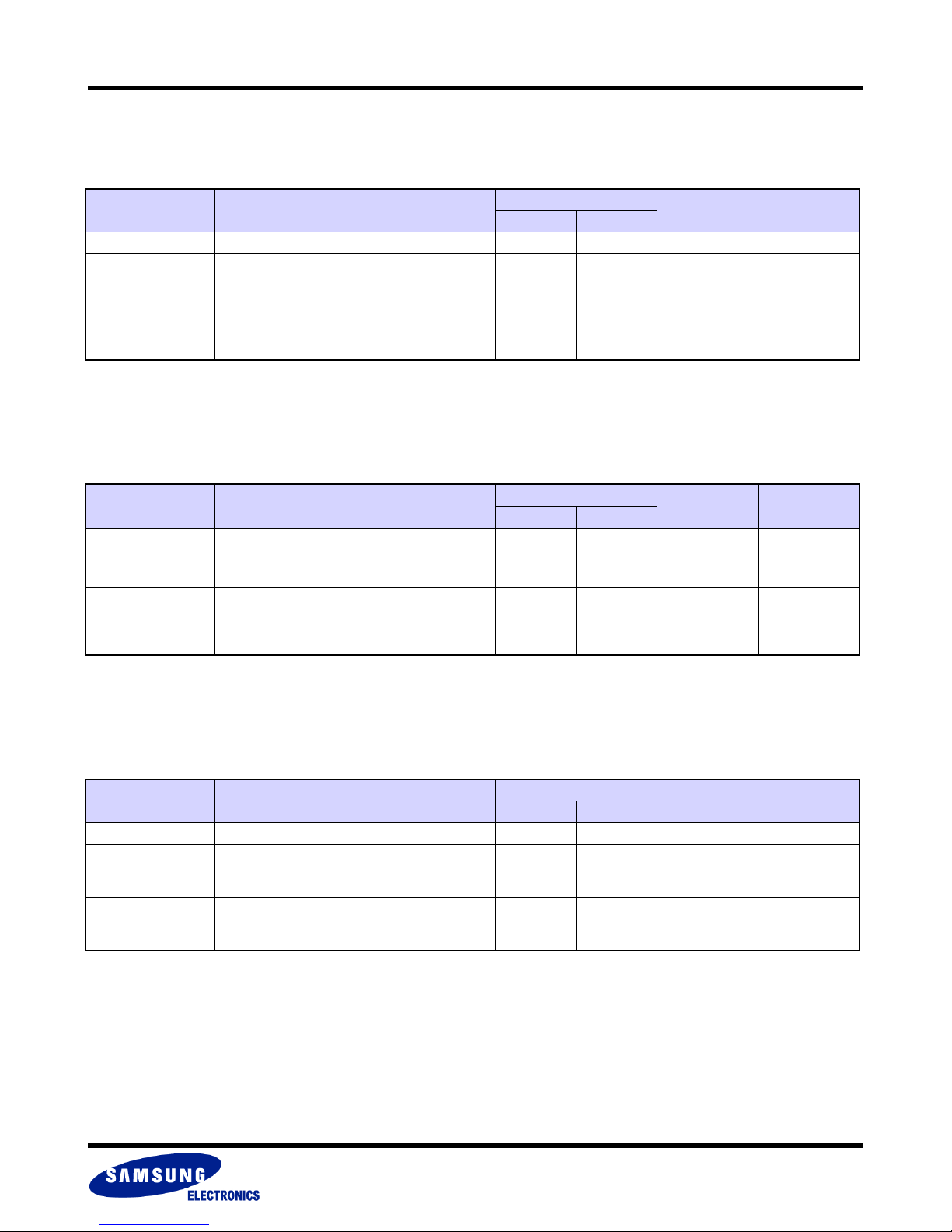
MuxOneNAND2G(KFM2G16Q2A-DEBx)
MuxOneNAND4G(KFN4G16Q2A-DEBx)
Write Interrupt (WI)
This is the Write interrupt bit.
WI Interrupt [6]
Status Conditions
sets itself to ‘1’
clears to ‘0’
Erase Interrupt (EI)
This is the Erase interrupt bit.
EI Interrupt [5]
Status Conditions
sets itself to ‘1’
clears to ‘0’
At the completion of an Program Operation
(0080h, 001Ah, 001Bh, 007Dh, 007Fh)
’0’ is written to this bit,
Cold/Warm/Hot reset is being performed, or command is written to Command Register in INT auto
mode
At the completion of an Erase Operation
(0094h, 0095h, 0030h)
’0’ is written to this bit,
Cold/Warm/Hot reset is being performed, or command is written to Command Register in INT auto
mode
FLASH MEMORY
Default State
Cold Warm/h ot
00 0 off
Default State
Cold Warm/hot
00 0 off
Valid
State
1
0
1
0
Valid
State
1
0
1
0
Interrupt
Function
Pending
off
Interrupt
Function
Pending
off
Reset Interrupt (RSTI)
This is the Reset interrupt bit.
RSTI Interrupt [4]
Status Conditions
sets itself to ‘1’
clears to ‘0’
command is written to Command Register in INT
At the completion of an Reset Operation
(00B0h, 00F0h, 00F3h or
warm reset is released)
’0’ is written to this bit, or
auto mode
Default State
Cold Warm/h ot
01 0 off
Valid
State
0
1
1
0
Interrupt
Function
Pending
off
- 76 -
Page 77
MuxOneNAND2G(KFM2G16Q2A-DEBx)
MuxOneNAND4G(KFN4G16Q2A-DEBx)
2.8.23 Start Block Address Register F24Ch (R/W)
This Read/Write register shows the NAND Flash block address in the Write Protection mode. Setting this register precedes a 'Lock Block'
command, 'Unlock Block' command, or ‘Lock-Tight' Command.
F24Ch, default = 0000h
15 14 13 12 11 10 9 8 7 6 5 4 3 2 1 0
Reserved(000000) SBA
Device Number of Block SBA
2Gb 2048 [10:0]
SBA Information[10:0]
Item Definition Description
SBA Start Block Address Precedes Lock Block, Unlock Block, or Lock-Tight commands
2.8.24 End Block Address Register F24Dh
FLASH MEMORY
This register is reserved for future use.
2.8.25 NAND Flash Write Protection Status Register F24Eh (R)
This Read register shows the Write Protection Status of the NAND Flash memory array.
To read the write protection status, FBA(DFS and DBS also in case of DDP) has to be set before reading the register
F24Eh, default = 0002h
15 14 13 12 11 10 9 8 7 6 5 4 3 2 1 0
Reserved(0000000000000) US LS LTS
Write Protection Status Information[2:0]
Item Definition Description
US Unlocked Status 1 = current NAND Flash block is unlocked
LS Locked Status
LTS Locked-Tight Status 1 = current NAND Flash block is locked-tight
1 = current NAND Flash block is locked
Or First Block of NAND Flash Array is Locked to be OTP
.
- 77 -
Page 78
MuxOneNAND2G(KFM2G16Q2A-DEBx)
MuxOneNAND4G(KFN4G16Q2A-DEBx)
2.8.26 ECC Status Register FF00h (R)
This Read register shows the Error Correction Status. The MuxOneNAND can detect 1- or 2-bit errors and correct 1-bit errors. 3-bit or more
error detection and correction is not supported.
ECC can be performed on the NAND Flash main and spare memory areas. The ECC status register can also show the number of errors in a
sector as a result of an ECC check in during a load operation. ECC status bits are also updated during a boot loading operation.
ECC registers will be reset when another command is issued.
FF00h, default = 0000h
15 14 13 12 11 10 9 8 7 6 5 4 3 2 1 0
ERm3 ERs3 ERm2 ERs2 ERm1 ERs1 ERm0
NOTE :
1) After Synchronous Block Burst Read operation, DQ[0] shows accmulated 1bit error.
Error Status
ERm, ERs ECC Status
00 No Error
01 1 bit error(correctable)
10 2 bit error (uncorrectable)
11 Rese rve d
FLASH MEMORY
1)
ERs0
ECC Information[15:0]
Item Definition Description
Status of errors in the 1st selected sector of the main BufferRAM
as a result of an ECC check during a load operation.
Also updated during a Bootload operation.
Status of errors in the 2nd selected sector of the main BufferRAM
as a result of an ECC check during a load operation.
Also updated during a Bootload operation.
Status of errors in the 3rd selected sector of the main BufferRAM
as a result of an ECC check during a load operation.
Also updated during a Bootload operation.
Status of errors in the 4th selected sector of the main BufferRAM
as a result of an ECC check during a load operation.
Also updated during a Bootload operation.
Status of errors in the 1st selected sector of the spare BufferRAM
as a result of an ECC check during a load operation.
Also updated during a Bootload operation.
Status of errors in the 2nd selected sector of the spare BufferRAM
as a result of an ECC check during a load operation.
Also updated during a Bootload operation.
Status of errors in the 3rd selected sector of the spare BufferRAM
as a result of an ECC check during a load operation.
Also updated during a Bootload operation.
Status of errors in the 4th selected sector of the spare BufferRAM
as a result of an ECC check during a load operation.
Also updated during a Bootload operation.
ERm0
ERm1
ERm2
ERm3
ERs0
ERs1
ERs2
ERs3
1st selected sector of
the main BufferRAM
2nd selected sector of
the main BufferRAM
3rd selected sector of
the main BufferRAM
4th selected sector of
the main BufferRAM
1st selected sector of
the spare BufferRAM
2nd selected sector of
the spare BufferRAM
3rd selected sector of
the spare BufferRAM
4th selected sector of
the spare BufferRAM
- 78 -
Page 79
MuxOneNAND2G(KFM2G16Q2A-DEBx)
MuxOneNAND4G(KFN4G16Q2A-DEBx)
2.8.27 ECC Result of 1st Selected Sector, Main Area Data Register FF01h (R)
This Read register shows the Error Correction result for the 1st selected sector of the main area data. ECCposWord0 is the error position
address in the Main Area data of 256 words. ECCposIO0 is the error position address which selects 1 of 16 DQs. ECCposWord0 and
ECCposIO0 are also updated at boot loading.
FF01h, default = 0000h
15 14 13 12 11 10 9 8 7 6 5 4 3 2 1 0
Reserved(0000) ECCposWord0 ECCposIO0
2.8.28 ECC Result of 1st Selected Sector, Spare Area Data Register FF02h (R)
This Read register shows the Error Correction result for the 1st selected sector of the spare area data. ECClogSector0 is the error position
address for 1.5 words of 2nd and 3rd words in the spare area. ECCposIO0 is the error position address which selects 1 of 16 DQs.
ECClogSector0 and ECCposIO0 are also updated at boot loading.
FF02h, default = 0000h
15 14 13 12 11 10 9 8 7 6 5 4 3 2 1 0
Reserved(0000000000) ECClogSector0 ECCposIO0
FLASH MEMORY
2.8.29 ECC Result of 2nd Selected Sector, Main Area Data Register FF03h (R)
This Read register shows the Error Correction result for the 2nd selected sector of the main area data. ECCposWord1 is the error position
address in the Main Area data of 256 words. ECCposIO1 is the error position address which selects 1 of 16 DQs. ECCposWord1 and
ECCposIO1 are also updated at boot loading.
FF03h, default = 0000h
15 14 13 12 11 10 9 8 7 6 5 4 3 2 1 0
Reserved(0000) ECCposWord1 ECCposIO1
2.8.30 ECC Result of 2nd Selected Sector, Spare Area Data Register FF04h (R)
This Read register shows the Error Correction result for the 2nd selected sector of the spare area data. ECClogSector1 is the error position
address for 1.5 words of 2nd and 3rd words in the spare area. ECCposIO1 is the error position address which selects 1 of 16 DQs.
ECClogSector1 and ECCposIO1 are also updated at boot loading.
FF04h, default = 0000h
15 14 13 12 11 10 9 8 7 6 5 4 3 2 1 0
Reserved(0000000000) ECClogSector1 ECCposIO1
- 79 -
Page 80
MuxOneNAND2G(KFM2G16Q2A-DEBx)
MuxOneNAND4G(KFN4G16Q2A-DEBx)
2.8.31 ECC Result of 3rd Selected Sector, Main Area Data Register FF05h (R)
This Read register shows the Error Correction result for the 3rd selected sector of the main area data. ECCposWord2 is the error position
address in the Main Area data of 256 words. ECCposIO2 is the error position address which selects 1 of 16 DQs. ECCposWord2 and
ECCposIO2 are also updated at boot loading.
FF05h, default = 0000h
15 14 13 12 11 10 9 8 7 6 5 4 3 2 1 0
Reserved(0000) ECCposWord2 ECCposIO2
FLASH MEMORY
2.8.32 ECC Result of 3
This Read register shows the Error Correction result for the 3rd selected sector of the spare area data. ECClogSector2 is the error position
address for 1.5 words of 2nd and 3rd words in the spare area. ECCposIO2 is the error position address which selects 1 of 16 DQs.
ECClogSector2 and ECCposIO2 are also updated at boot loading.
FF06h, default = 0000h
15 14 13 12 11 10 9 8 7 6 5 4 3 2 1 0
rd
Selected Sector, Spare Area Data Register FF06h (R)
Reserved(0000000000) ECClogSector2 ECCposIO2
2.8.33 ECC Result of 4th Selected Sector, Main Area Data Register FF07h (R)
This Read register shows the Error Correction result for the 4th selected sector of the main area data. ECCposWord3 is the error position
address in the Main Area data of 256 words. ECCposIO3 is the error position address which selects 1 of 16 DQs. ECCposWord3 and
ECCposIO3 are also updated at boot loading.
FF07h, default = 0000h
15 14 13 12 11 10 9 8 7 6 5 4 3 2 1 0
Reserved(0000) ECCposWord3 ECCposIO3
2.8.34 ECC Result of 4th Selected Sector, Spare Area Data Register FF08h (R)
This Read register shows the Error Correction result for the 4th selected sector of the spare area data. ECClogSector3 is the error position
address for 1.5 words of 2nd and 3rd words in the spare area. ECCposIO3 is the error position address which selects 1 of 16 DQs.
ECClogSector3 and ECCposIO3 are also updated at boot loading.
FF08h, default = 0000h
15 14 13 12 11 10 9 8 7 6 5 4 3 2 1 0
Reserved(0000000000) ECClogSector3 ECCposIO3
- 80 -
Page 81
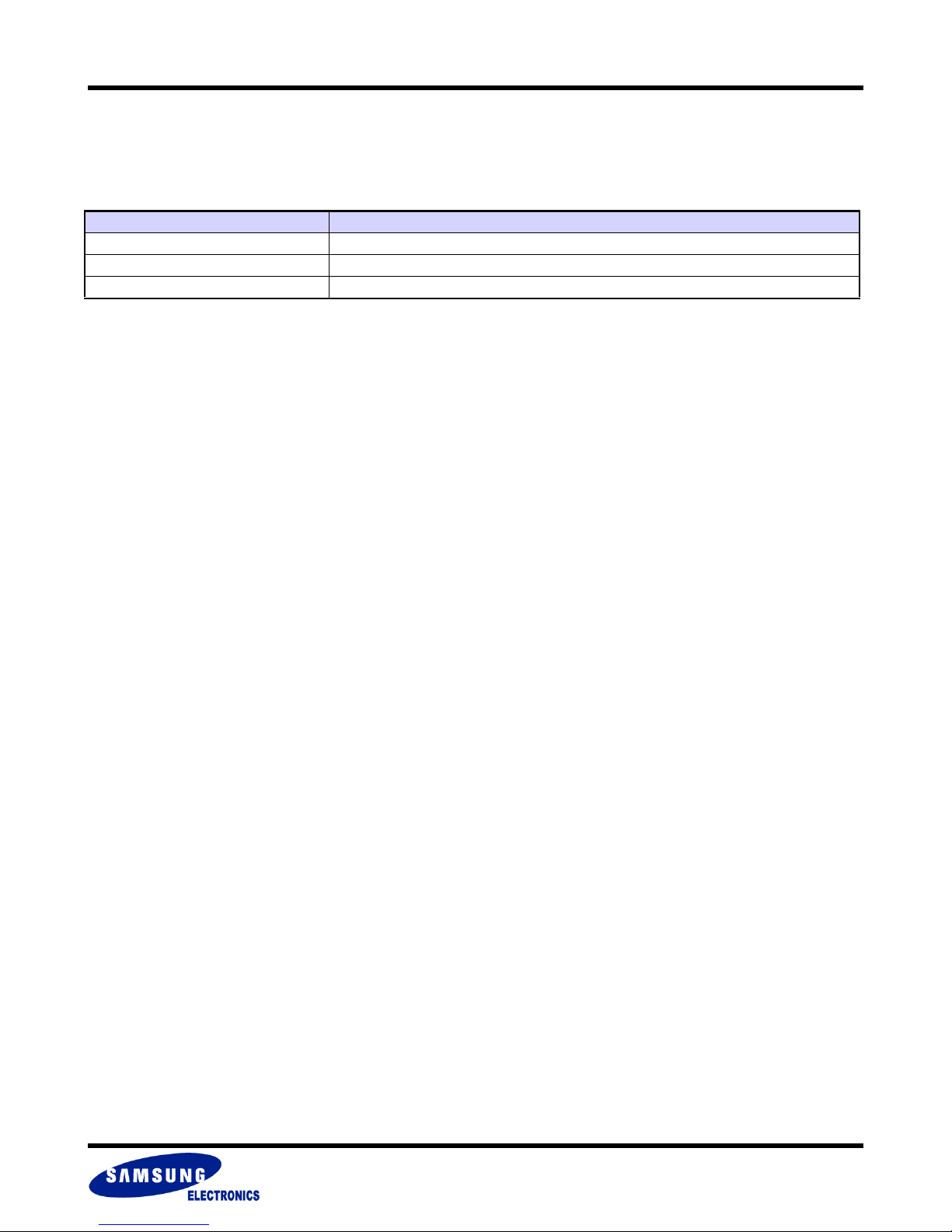
MuxOneNAND2G(KFM2G16Q2A-DEBx)
MuxOneNAND4G(KFN4G16Q2A-DEBx)
ECC Log Sector
ECClogSector0~ECClogSector3 indicates the error position in the 2nd word and LSB of 3rd word in the spare area.
Refer to note 2 in chapter 2.7.2
ECClogSector Information [5:4]
ECClogSector Error Position
00 2nd word
01 3rd word
10, 11 Reserved
FLASH MEMORY
- 81 -
Page 82
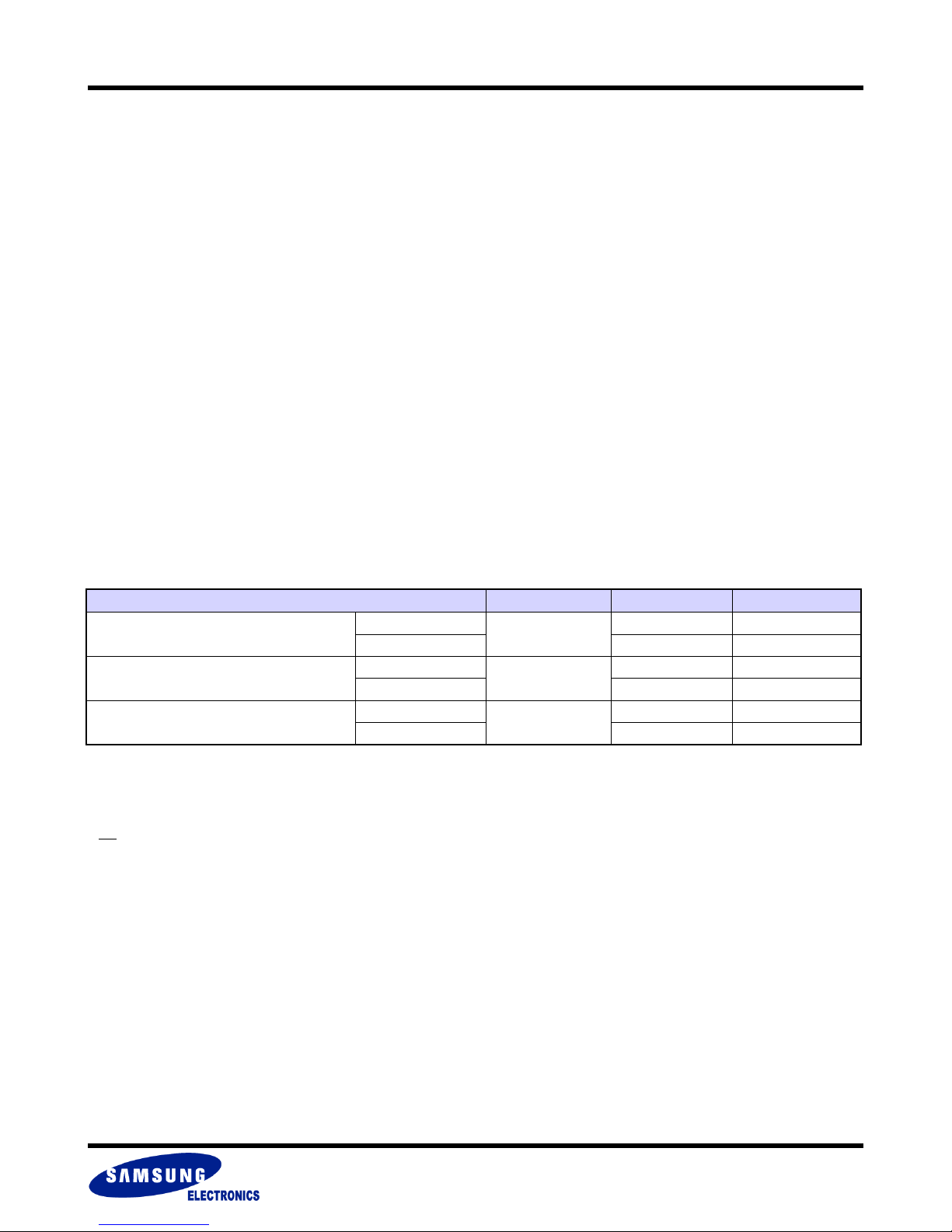
MuxOneNAND2G(KFM2G16Q2A-DEBx)
MuxOneNAND4G(KFN4G16Q2A-DEBx)
FLASH MEMORY
3.0 DEVICE OPERATION
This section of the datasheet discusses the operation of the MuxOneNAND device. It is followed by AC/DC
Characteristics and Timing Diagrams which may be consulted for further information.
The MuxOneNAND supports a limited command-based interface in addition to a register-based interface for performing operations on the
device.
3.1 Command Based Operation
The command-based interface is active in the boot partition. Commands can only be written with a boot area address. Boot area data is only
returned if no command has been issued prior to the read.
The entire address range, except for the boot area, can be used for the data buffer. All commands are written to the boot partition. Writes outside the boot partition are treated as normal writes to the buffers or registers.
The command consists of one or more cycles depending on the command. After completion of the command the device starts its execution.
Writing incorrect information including address and data to the boot partition or writing an improper command will terminate the previous command sequence and make the device enter the ready status.
The defined valid command sequences are stated in Command Sequences Table.
Command based operations are mainly used when MuxOneNAND is used as Booting device, and all command based operations only supports asynchronous reads and writes. With DDP, command based operation except reset is applicable only on chip1.
Command Sequences
Command Definition Cycles 1st cycle 2nd cycle
Reset MuxOneNAND
Load Data into Buffer
Read Identification Data
NOTE :
1) BP(Boot Partition) : BootRAM Area [0000h ~ 01FFh, 8000h ~ 800Fh]. (Chip 1 only in case of DDP)
2) Load Data into Buffer operation is available within a block(128KB) (Chip1 only in case of DDP)
3) Load 2KB unit into DataRAM0. Current Start address(FPA) is automatically incremented by 2KB unit after the load.
4) 0000h -> Data is Manufacturer ID (Chip1 only in case of DDP)
0001h -> Data is Device ID (Chip1 only in case of DDP)
0002h -> Current Block Write Protection Status (Chip1 only in case of DDP)
toggling can terminate ‘Read Identification Data’ operation.
5) WE
2)
5)
Add
Data 00F0h
Add
Data 00E0h
Add
Data 0090h Data
1
2
2
1)
BP
BP BP
0000h
BP
XXXXh
3)
4)
- 82 -
Page 83
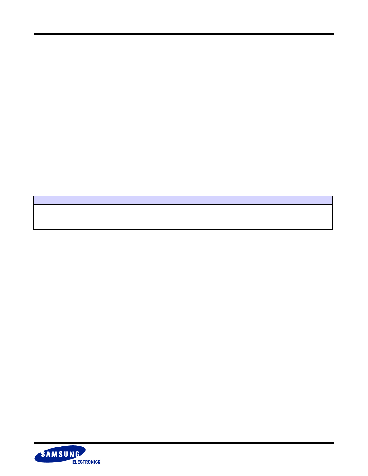
MuxOneNAND2G(KFM2G16Q2A-DEBx)
MuxOneNAND4G(KFN4G16Q2A-DEBx)
3.1.1 Reset MuxOneNAND Command
The Reset command is given by writing 00F0h to the boot partition address. Reset will return all default values into the device.
3.1.2 Load MuxOneNAND Command
Load Data into Buffer command is a two-cycle command. Two sequential designated command activates this operation. Sequentially writing
00E0h and 0000h to the boot partition [0000h~01FFh, 8000h~800Fh] will load one page to DataRAM0. This operation refers to FBA and FPA.
FSA, BSA, and BSC are not considered.
At the end of this operation, FPA will be automatically increased by 1. So continuous issue of this command will sequentially load data in next
page to DataRAM0. This page address increment is restricted within a block.
The default value of FBA and FPA is 0. Therefore, initial issue of this command after power on will load the first page of memory, which is usually boot code.
3.1.3 Read Identification Data Command
The Read Identification Data command consists of two cycles. It gives out the devices identification data according to the given address. The
first cycle is 0090h to the boot partition address and second cycle is read from the addresses specified in Identification Data Description Table.
Identification Data Description
Address Data Out
0000h Manufacturer ID (00ECh)
0001h
0002h
NOTE :
1) Refer to Device ID Register (Chapter 2.8.3)
2)To read the write protection status, FBA has to be set before issuing this command.
Current Block Write Protection Status
Device ID
FLASH MEMORY
1)
2)
- 83 -
Page 84
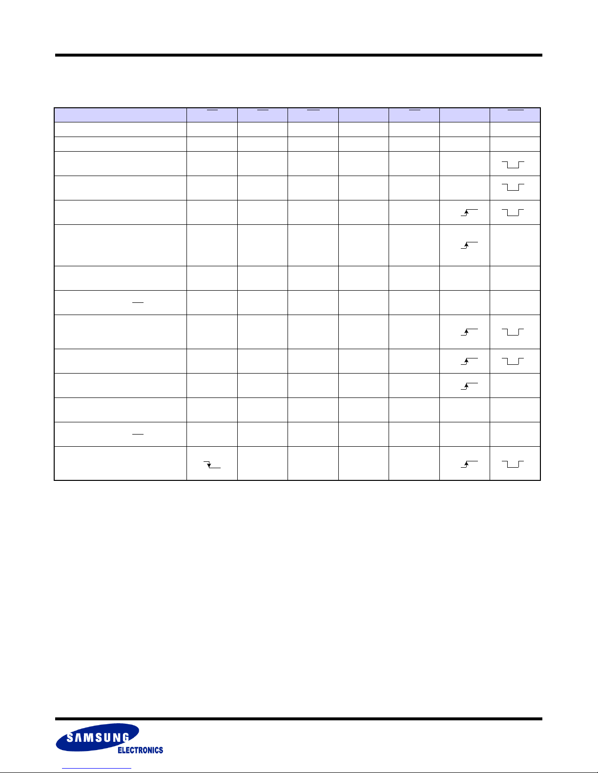
MuxOneNAND2G(KFM2G16Q2A-DEBx)
MuxOneNAND4G(KFN4G16Q2A-DEBx)
3.2 Device Bus Operation
The device bus operations are shown in the table below.
Operation CE OE WE ADQ0~15 RP CLK AV D
Standby H X X High-Z H X X
Warm Reset X X X High-Z L X X
Asynchronous Write L H L
Asynchronous Read L L H
Start Initial Burst Read L H H Add. In H
Add. In /Data
Add. In /Data
In
Out
FLASH MEMORY
HL
HL
Burst Read L L H
Terminate Burst Read
Cycle
Terminate Burst Read
Cycle via RP
Terminate Current Burst
Read Cycle and Start
New Burst Read Cycle
Start Initial Burst Write L H L Add In H
Burst Write L H X Data In H H
Terminate Burst Write
Cycle
Terminate Burst Write
Cycle via RP
Terminate Current Burst
Write Cycle and Start
New Burst Write Cycle
NOTE :
L=VIL (Low), H=VIH (High), X=Don’t Care.
HXHHigh-ZHXX
XXXHigh-ZL XX
L H H Add In H
HHXHigh-ZHXX
XXXHigh-ZL XX
H L Add In H
Burst Data
Out
H
H
- 84 -
Page 85
MuxOneNAND2G(KFM2G16Q2A-DEBx)
MuxOneNAND4G(KFN4G16Q2A-DEBx)
3.3 Reset Mode Operation
The One NAND has 4 reset modes: Cold/Warm/Hot Reset, and NAND Flash Array Reset. Section 3.3 discusses the operation of these reset
modes.
The Register Reset Table shows the which registers are affected by the various types or Reset operations.
Internal Register Reset Table
Warm
Internal Registers Default Cold Reset
F000h Manufacturer ID Register (R) 00ECh N/A N/A N/A N/A
F001h Device ID Register (R): MuxOneNAND (Note 3) N/A N/A N/A N/A
F002h Version ID Register (R) N/A N/A N/A N/A N/A
F003h Data Buffer size Register (R) 0800h N/A N/A N/A N/A
F004h Boot Buffer size Register (R) 0200h N/A N/A N/A N/A
F005h Amount of Buffers Register (R) 0201h N/A N/A N/A N/A
F006h Technology Register (R) 0000h N/A N/A N/A N/A
F100h Start Address1 Register (R/W): DFS, FBA 0000h 0000h 0000h 0000h N/A
F101h Start Address2 Register (R/W): DBS 0000h 0000h 0000h 0000h N/A
F102h Start Address3 Register (R/W): FCBA 0000h 0000h 0000h 0000h N/A
F103h Start Address4 Register (R/W): FCPA, FCSA 0000h 0000h 0000h 0000h N/A
F104h Start Address5 Register (R/W): FPC 0000h 0000h 0000h 0000h N/A
F107h Start Address8 Register (R/W): FPA, FSA 0000h 0000h 0000h 0000h N/A
F200h Start Buffer Register (R/W): BSA, BSC 0000h 0000h 0000h 0000h N/A
F220h Command Register (R/W) 0000h 0000h 0000h 0000h N/A
F221h System Configuration 1 Register (R/W) 40C0h 40C0h (Note1a) (Note1a) N/A
F240h Controller Status Register (R) (Note 1b)(Note 4) 0000h 0000h 0000h 0000h N/A
F241h Interrupt Status Register (R/W) - 8080h 8010h 8010h N/A
F24Ch Start Block Address (R/W) 0000h 0000h 0000h N/A N/A
F24Dh End Block Address: N/A N/A N/A N/A N/A N/A
F24Eh NAND Flash Write Protection Status (R) (Note 5) 0002h 0002h 0002h N/A N/A
FF00h ECC Status Register (R) (Note2) 0000h 0000h 0000h 0000h N/A
FF01h
FF02h
FF03h
FF04h
FF05h
FF06h
FF07h
FF08h
NOTE :
1a) RDYpol, RDY conf, INTpol, IOBE are reset by Cold reset. The other bits are reset by cold/warm/hot reset.
1b) The other bits except OTP
2) ECC Status Register & ECC Result Registers are reset when any command is issued.
3) Refer to Device ID Register F001h.
4) Resetting during IDLE state, this is valid. But resetting during BUSY state, refer to Chapter 2.8.21.
5) To read NAND Flash Write Protection status, Block Address register must be written before.
ECC Result of Sector 0 Main area data Regis-
ECC Result of Sector 0 Spare area data Regis-
ECC Result of Sector 1 Main area data Regis-
ECC Result of Sector 1 Spare area data Regis-
ECC Result of Sector 2 Main area data Regis-
ECC Result of Sector 2 Spare area data Regis-
ECC Result of Sector 3 Main area data Regis-
ECC Result of Sector 3 Spare area data Regis-
and OTPBL are reset by cold/warm/hot reset.
L
0000h 0000h 0000h 0000h N/A
0000h 0000h 0000h 0000h N/A
0000h 0000h 0000h 0000h N/A
0000h 0000h 0000h 0000h N/A
0000h 0000h 0000h 0000h N/A
0000h 0000h 0000h 0000h N/A
0000h 0000h 0000h 0000h N/A
0000h 0000h 0000h 0000h N/A
Reset
(RP
)
FLASH MEMORY
Hot
Reset
(00F3h)
Hot
Reset
(BP-F0h)
NAND Flash
Core Reset
(00F0h)
- 85 -
Page 86
MuxOneNAND2G(KFM2G16Q2A-DEBx)
MuxOneNAND4G(KFN4G16Q2A-DEBx)
3.3.1 Cold Reset Mode Operation
See Timing Diagram 6.17
At system power-up, the voltage detector in the device detects the rising edge of Vcc and releases an internal power-up reset signal. This triggers bootcode loading. Bootcode loading means that the boot loader in the device copies designated sized data (1KB) from the beginning of
memory into the BootRAM. This sequence is the Cold Reset of MuxOneNAND.
The POR(Power On Reset) triggering level is typically 1.5V. Boot code copy operation activates 400us after POR.
Therefore, the system power should reach 1.7V within 400us from the POR triggering level for bootcode data to be valid.
It takes approximately 70us to copy 1KB of bootcode. Upon completion of loading into the BootRAM, it is available to be read by the host. The
INT pin is not available until after IOBE = 1 and IOBE bit can be changed by host.
3.3.2 Warm Reset Mode Operation
See Timing Diagrams 6.18
FLASH MEMORY
A Warm Reset means that the host resets the device by using the RP
ations and executes internal reset operation and resets current NAND Flash core operation synchronized with the falling edge of RP
During an Internal Reset Operation, the device initializes internal registers and makes output signals go to default status.
The BufferRAM data is kept unchanged after Warm/Hot reset operations.
The device guarantees the logic reset operation in case RP
The device may reset if tRP < tRP min(200ns), but this is not guaranteed.
Warm reset will abort the current NAND Flash core operation. During a warm reset, the content of memory cells being altered is no longer
valid as the data will be partially programmed or erased.
Warm reset has no effect on contents of BootRAM and DataRAM.
pulse is longer than tRP min(200ns).
pin. When the a RP low is issued, the device logic stops all current oper-
.
3.3.3 Hot Reset Mode Operation
See Timing Diagram 6.19
A Hot Reset means that the host resets the device by Reset command. The reset command can be either Command based or Register
Based. Upon receiving the Reset command, the device logic stops all current operation and executes an internal reset operation and resets
the current NAND Flash core operation.
During an Internal Reset Operation, the device initializes internal registers and makes output signals go to default status. The BufferRAM data
is kept unchanged after Warm/Hot reset operations.
Hot reset has no effect on contents of BootRAM and DataRAM.
3.3.4 NAND Flash Core Reset Mode Operation
See Timing Diagram 6.20
The Host can reset the NAND Flash Core operation by issuing a NAND Flash Core reset command. NAND Flash core reset will abort the current NAND Flash core operation. During a NAND Flash core reset, the content of memory cells being altered is no longer valid as the data will
be partially programmed or erased.
NAND Flash Core Reset has an effect on neither contents of BootRAM and DataRAM nor register values.
- 86 -
Page 87
MuxOneNAND2G(KFM2G16Q2A-DEBx)
MuxOneNAND4G(KFN4G16Q2A-DEBx)
3.4 Write Protection Operation
The MuxOneNAND can be write-protected to prevent re-programming or erasure of data.
The areas of write-protection are the BootRAM, and the NAND Flash Array.
3.4.1 BootRAM Write Protection Operation
At system power-up, voltage detector in the device detects the rising edge of Vcc and releases the internal power-up reset signal which triggers bootcode loading. And the designated size data(1KB) is copied from the first page of the first block in the NAND flash array to the
BootRAM.
After the bootcode loading is completed, the BootRAM is always locked to protect the boot code from the accidental write.
3.4.2 NAND Flash Array Write Protection Operation
The device has both hardware and software write protection of the NAND Flash array.
Hardware Write Protection Operation
The hardware write protection operation is implemented by executing a Cold or Warm Reset. On power up, the NAND Flash Array is in its
default, locked state. The entire NAND Flash array goes to a locked state after a Cold or Warm Reset.
FLASH MEMORY
Software Write Protection Operation
The software write protection operation is implemented by writing a Lock command (002Ah) or a Lock-tight command (002Ch) to command
register (F220h).
Lock (002Ah) and Lock-tight (002Ch) commands write protects the block defined in the Start Block Address Register F24Ch.
3.4.3 NAND Array Write Protection States
There are three lock states in the NAND Array: unlocked, locked, and locked-tight.
MuxOneNAND supports lock/unlock/lock-tight by one block, and All Block Unlock at once. If any blocks are changed to locked-tight state, the
all block unlock command will fail. In order to use all block unlock command again, a cold reset is needed.
Write Protection Status
The current block Write Protection status can be read in NAND Flash Write Protection Status Register(F24Eh). There are three bits - US, LS,
LTS -, which are not cleared by hot reset. These Write Protection status registers are updated when FBA is set, and when Write Protection
command is entered.
The followings summarize locking status.
example)
In default, [2:0] values are 010.
-> If host executes unlock block operation, then [2:0] values turn to 100.
-> If host executes lock-tight block operation, then [2:0] values turn to 001.
- 87 -
Page 88
MuxOneNAND2G(KFM2G16Q2A-DEBx)
MuxOneNAND4G(KFN4G16Q2A-DEBx)
3.4.3.1 Unlocked NAND Array Write Protection State
An Unlocked block can be programmed or erased. The status of an unlocked block can be changed to locked or locked-tight using the appropriate software command. (locked-tight state can be achieved via lock-tight command which follows lock command)
Only one block can be released from lock state to unlock state with Unlock command and addresses. The unlocked block can be changed
with new lock command. Therefore, each block has its own lock/unlock/lock-tight state.
If any blocks are changed to locked-tight state, the all block unlock command will fail. In order to use all block unlock command again, a cold
reset is needed.
Unlocked
Unlock Command Sequence:
Start block address+Unlock block command (0023h)
Unlocked
FLASH MEMORY
All Block Unlock Command Sequence:
Start block address(000h)+All Block Unlock command (0027h)
NOTE :
Even though SBA is fixed to 000h, Unlock will be done for allblock.
3.4.3.2 Locked NAND Array Write Protection State
A Locked block cannot be programmed or erased. All blocks default to a locked state following a Cold or Warm Reset. Unlocked blocks can be
changed to locked using the Lock block command. The status of a locked block can be changed to unlocked or locked-tight using the appropriate software command.
Locked
Lock Command Sequence:
Start block address+Lock block command (002Ah)
- 88 -
Page 89
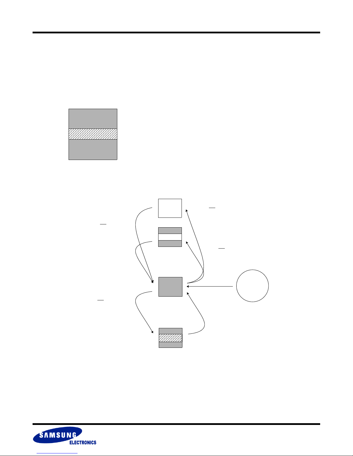
MuxOneNAND2G(KFM2G16Q2A-DEBx)
MuxOneNAND4G(KFN4G16Q2A-DEBx)
3.4.3.3 Locked-tight NAND Array Write Protection State
A block that is in a locked-tight state can only be changed to locked state after a Cold or Warm Reset. Unlock and Lock command sequences
will not affect its state. This is an added level of write protection security. If any blocks are changed to locked-tight state, the all block unlock
command will fail. In order to use all block unlock command again, a cold reset is needed.
A block must first be set to a locked state before it can be changed to locked-tight using the Lock-tight command.
Locked-tight
Lock-Tight Command Sequence:
Start block address+Lock-tight block command (002Ch)
3.4.4 NAND Flash Array Write Protection State Diagram
FLASH MEMORY
RP
pin: High
&
Start block address
Lock block Command
or
Cold reset or
Warm reset
RP
pin: High
&
Start block address
+Lock-tight block Command
*NOTE : If the 1st Block is set to be OTP, Block 0 will always be Lock Status
unlock
Lock
unlock
Lock
Lock
Lock
Lock-tight
Lock
pin: High
RP
Start block address (000h)
+All Block Unlock Command
Cold reset or
Warm reset
&
pin: High
RP
Start block address
+Unlock block Command
&
Power On
- 89 -
Page 90
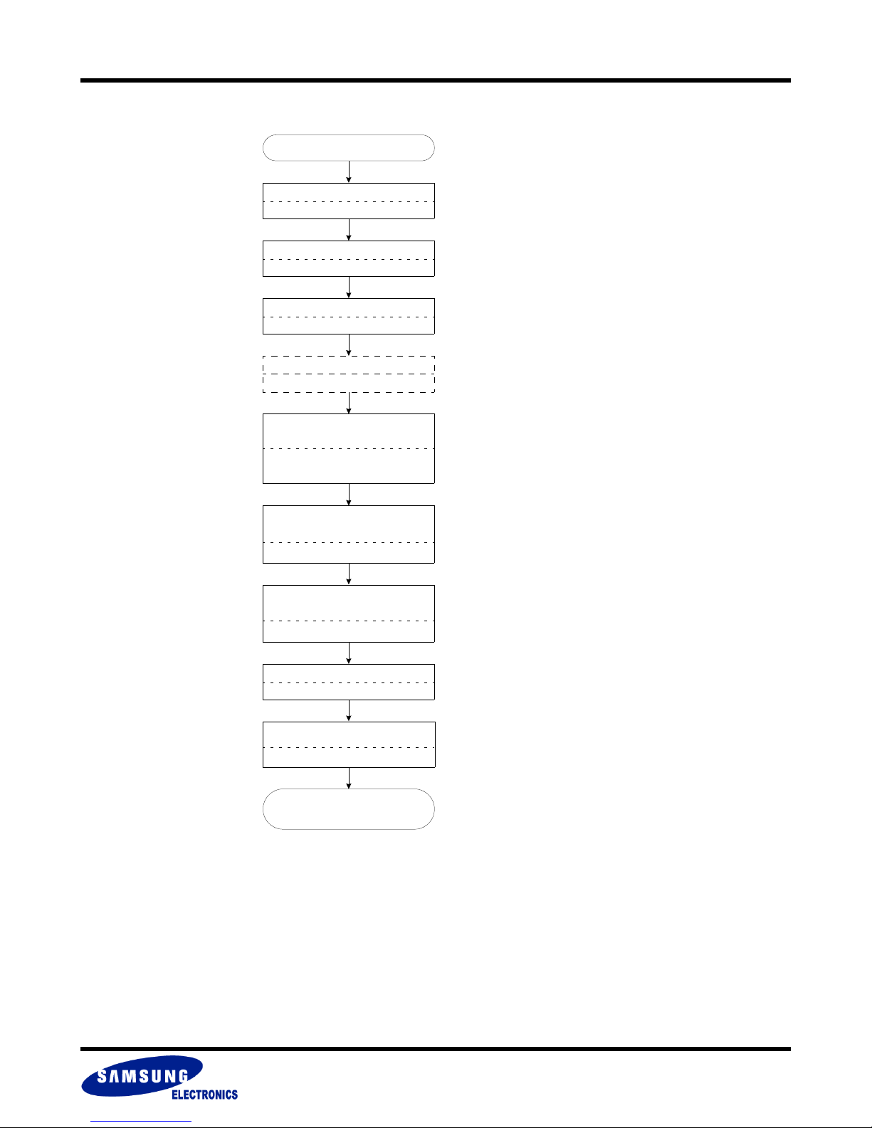
MuxOneNAND2G(KFM2G16Q2A-DEBx)
MuxOneNAND4G(KFN4G16Q2A-DEBx)
Data Protection Operation Flow Diagram
Start
Select DataRAM for DDP
Add: F101h DQ=DBS*
Write ‘DFS*’, of Flash
Add: F100h DQ=DFS*
Write ‘SBA’ of Flash
Add: F24Ch DQ=SBA
FLASH MEMORY
Write 0 to interrupt register
Add: F241h DQ=0000h
Write ‘lock/unlock/lock-tight’
Command
Add: F220h
DQ=002Ah/0023h/002Ch
Wait for INT register
low to high transition
Add: F241h DQ[15]=INT
Read Controller
Status Register
Add: F240h DQ[10]=0(pass)
Write ’DFS*’, ’FBA’ of Flash
Add: F100h DQ=DFS, FBA
Read Write Protection Register
Add: F24Eh DQ[2:0]=US,LS,LTS
1)
Lock/Unlock/Lock-Tight
* Samsung strongly recommends to follow the above flow chart
NOTE :
1) ‘Write 0 to interrupt register’ step may be ignored when using INT auto mode. Refer to chapter 2.8.18.1
completed
* DFS, DBS is for DDP
(DFS must be same)
- 90 -
Page 91
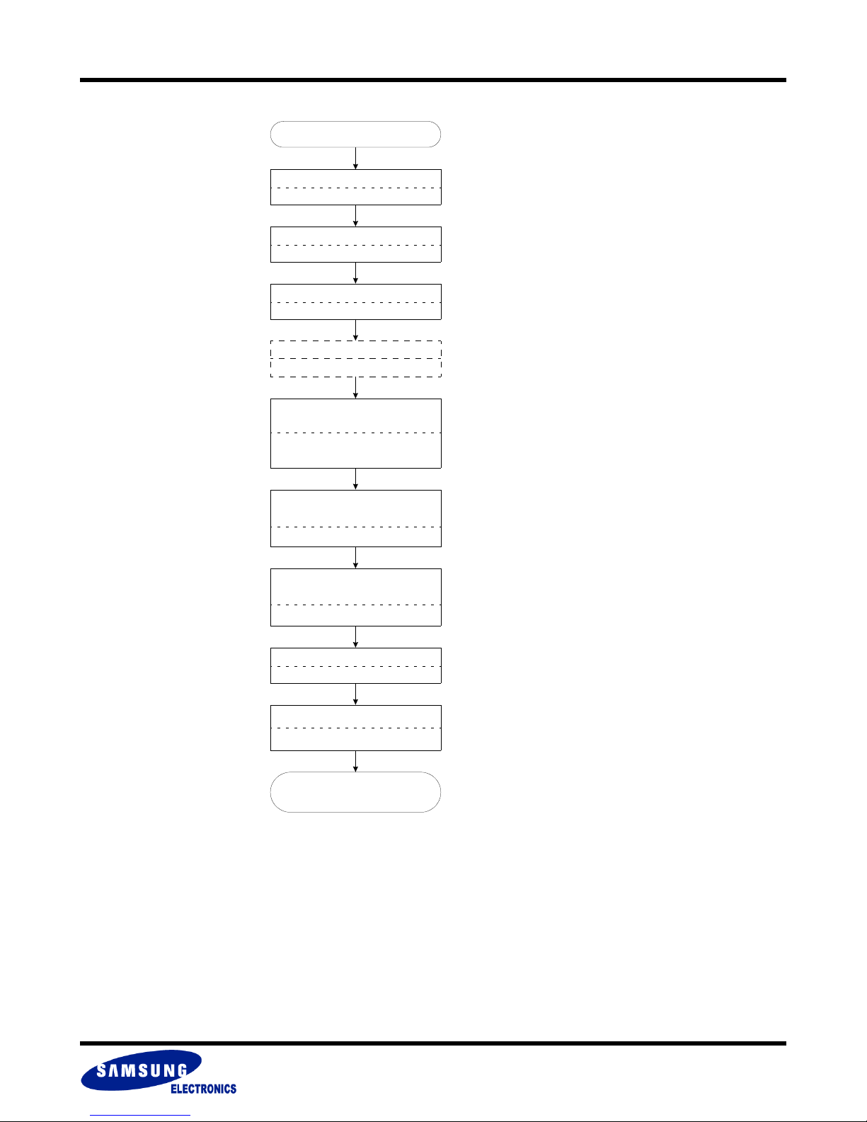
MuxOneNAND2G(KFM2G16Q2A-DEBx)
MuxOneNAND4G(KFN4G16Q2A-DEBx)
All Block Unlock Flow Diagram
Start
Select DataRAM for DDP
Add: F101h DQ=DBS*
Write ‘DFS*’, of Flash
Add: F100h DQ=DFS*
Write ‘SBA’ of Flash
Add: F24Ch DQ=SBA(000h)
FLASH MEMORY
Write 0 to interrupt register
Add: F241h DQ=0000h
Write ‘All Block Unlock’
Command
Add: F220h
DQ=0027h
Wait for INT register
low to high transition
Add: F241h DQ[15]=INT
Read Controller
Status Register
Add: F240h DQ[10]=0(pass)
Write ’DFS*’, ’FBA’ of Flash
Add: F100h DQ=DFS, FBA
Read Write Protection Register
Add: F24Eh DQ[2:0]=US,LS,LTS
1)
* Samsung strongly recommends to follow the above flow chart
* * If any blocks are changed to locked-tight state, the all block unlock command will fail.
In order to use all block unlock command again, a cold reset is needed.
NOTE :
1) ‘Write 0 to interrupt register’ step may be ignored when using INT auto mode. Refer to chapter 2.8.18.1
Unlock All Block
completed
* DFS, DBS is for DDP
(DFS must be same)
- 91 -
Page 92
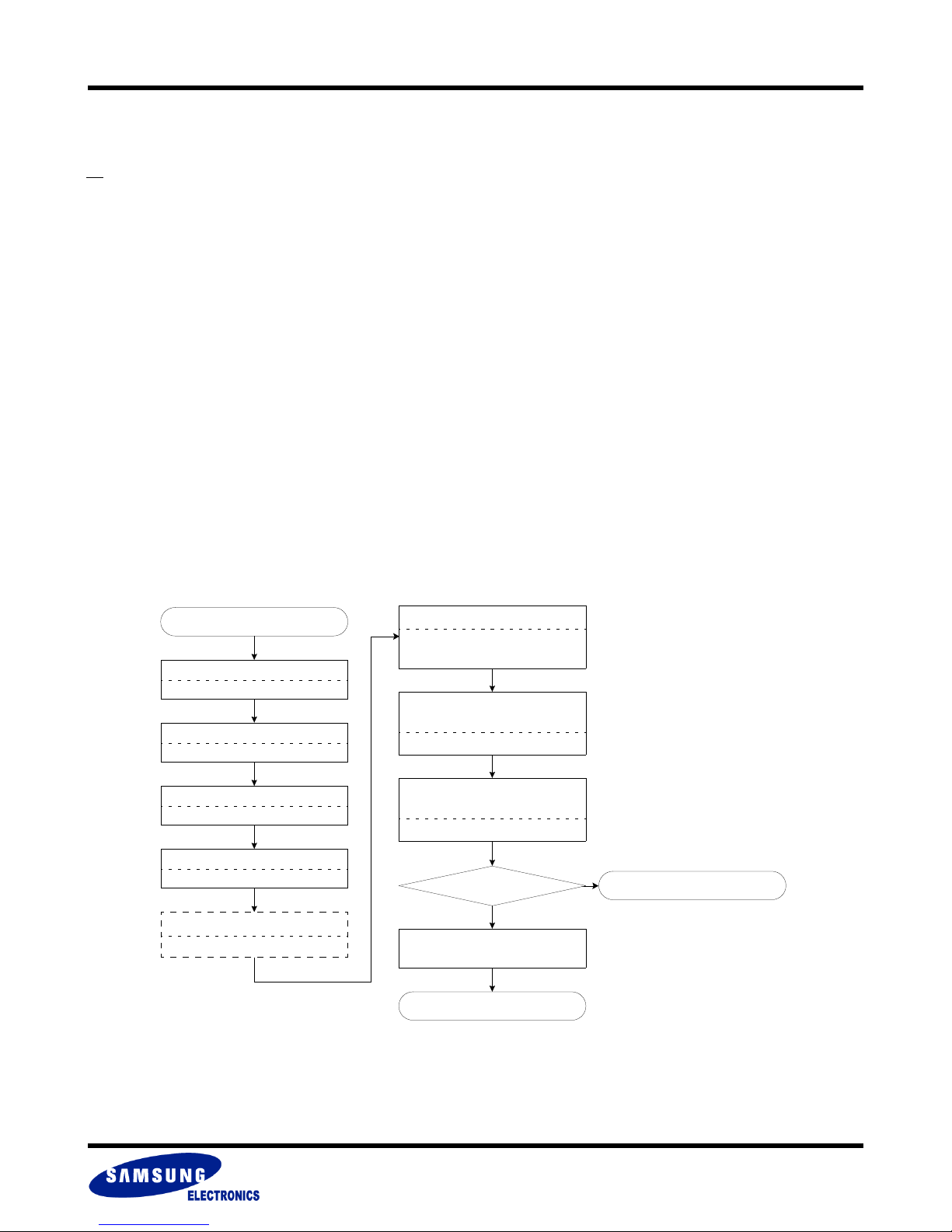
MuxOneNAND2G(KFM2G16Q2A-DEBx)
MuxOneNAND4G(KFN4G16Q2A-DEBx)
3.5 Data Protection During Power Down Operation
See Timing Diagram 6.21
The device is designed to offer protection from any involuntary program/erase during power-transitions.
pin which provides hardware protection is recommended to be kept at VIL before Vcc drops to 1.5V.
RP
3.6 Load Operation
See Timing Diagrams 6.11
The Load operation is initiated by setting up the start address from which the data is to be loaded. The Load command is issued in order to initiate the load.
During a Load operation, the device:
-Transfers the data from NAND Flash array into the BufferRAM
-ECC is checked and any detected and corrected error is reported in the status response as well as
any unrecoverable error.
Once the BufferRAM has been filled, an interrupt is issued to the host so that the contents of the BufferRAM can be read. The read from the
BufferRAM can be an asynchronous read mode or synchronous read mode. The status information related to load operation can be checked
by the host if required.
The device has a dual data buffer memory architecture (DataRAM0, DataRAM1), each 2KB in size. Each DataRAM buffer has 4
Sectors. The device is capable of independent and simultaneous data-read operation from one data buffer and data-load operation to the
other data buffer. Refer to the information for more details in section 3.15.1, "Read-While-Load Operation".
FLASH MEMORY
Load Operation Flow Chart Diagram
Start
Select DataRAM for DDP
Add: F101h DQ=DBS
Write ‘DFS*, FBA’ of Flash
Add: F100h DQ=DFS, FBA
Write ‘FPA, FSA’ of Flash
Add: F107h DQ=FPA, FSA
Write ‘BSA, BSC’ of DataRAM
Add: F200h DQ=BSA, BSC
Write 0 to interrupt register
Add: F241h DQ=0000h
NOTE :
1) ‘Write 0 to interrupt register’ step may be ignored when using INT auto mode. Refer to chapter 2.8.18.1
1)
Write ‘Load’ Command
Add: F220h
DQ=0000h or 0013h
Wait for INT register
low to high transition
Add: F241h DQ[15]=INT
Read Controller
Status Register
Add: F240h DQ[10]=Error
DQ[10]=0?
YES
Host reads data from
DataRAM
Read completed
NO
Map Out
* DBS, DFS is for DDP
- 92 -
Page 93
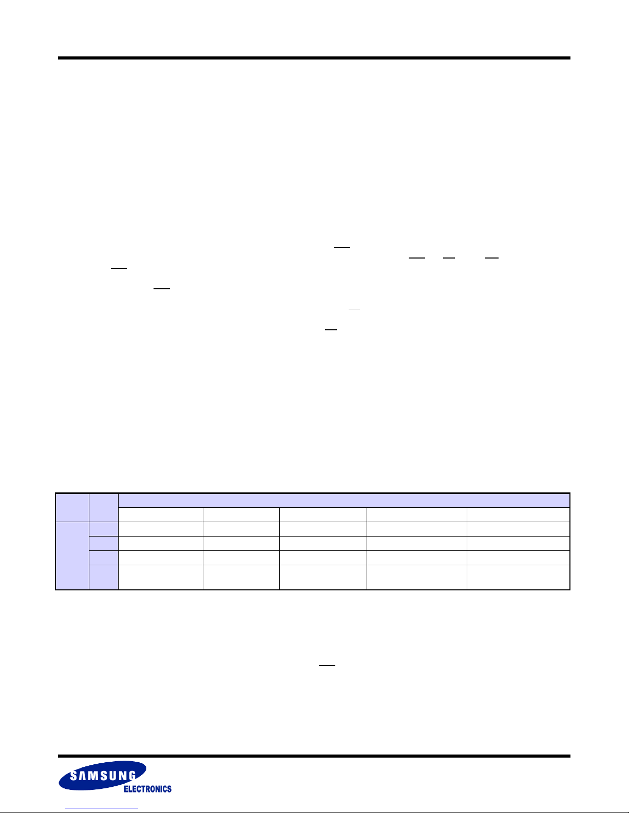
MuxOneNAND2G(KFM2G16Q2A-DEBx)
MuxOneNAND4G(KFN4G16Q2A-DEBx)
3.7 Read Operation
See Timing Diagrams 6.1, 6.2, 6.5, and 6.6
The device has two read modes; Asynchronous Read and Synchronous Burst Read.
The initial state machine automatically sets the device into the Asynchronous Read Mode (RM=0) to prevent the spurious altering of memory
content upon device power up or after a Hardware reset. No commands are required to retrieve data in Asynchronous Read Mode.
The Synchronous Read Mode is enabled by setting RM bit of System Configuration1 Register (F221h) to Synchronous Read Mode (RM=1).
See Section 2.8.19 for more information about System Configuration1 Register.
3.7.1 Asynchronous Read Mode Operation (RM=0, WM=0)
See Timing Diagrams 6.5 and 6.6
FLASH MEMORY
In an Asynchronous Read Mode, data is output with respect to a logic input, AVD
Output data will appear on DQ15-DQ0 when a valid address is asserted on A15-A0 while driving AVD
function of the AVD
Address access time from AVD
The Chip Enable access time (tCE) is equal to the delay from the falling edge of CE
The Output Enable access time (tOE) is the delay from the falling edge of OE
signal is to latch the valid address.
low (tAA) is equal to the delay from valid addresses to valid output data.
.
and CE to VIL. WE is held at VIH. The
to valid data at the outputs.
to valid data at the output.
3.7.2 Synchronous Read Mode Operation (RM=1, WM=X)
See Timing Diagrams 6.1 and 6.2
In a Synchronous Read Mode, data is output with respect to a clock input.
The device is capable of a continuous linear burst operation and a fixed-length linear burst operation of a preset length. Burst address
sequences for continuous and fixed-length burst operations are shown in the table below.
Burst Address Sequences
Burst Address Sequence(Decimal)
.
.
.
.
.
.
Wrap
around
Start
Addr.
Continuous Burst 4-word Burst 8-word Burst 16-word Burst 32-word Burst
0 0-1-2-3-4-5-6-..-0-1... 0-1-2-3-0... 0-1-2-3-4-5-6-7-0... 0-1-2-3-4-....-13-14-15-0... 0-1-2-3-4-....-29-30-31-0...
1 1-2-3-4-5-6-7-..-1-2... 1-2-3-0-1... 1-2-3-4-5-6-7-0-1... 1-2-3-4-5-....-14-15-0-1... 1-2-3-4-5-....-30-31-0-1...
2 2-3-4-5-6-7-8-..-2-3... 2-3-0-1-2... 2-3-4-5-6-7-0-1-2... 2-3-4-5-6-....-15-0-1-2... 2-3-4-5-6-....-31-0-1-2...
.
.
.
.
.
.
In the burst mode, the initial word will be output asynchronously, regardless of BRWL. While the following words will be determined by BRWL
value.
The latency is determined by the host based on the BRWL bit setting in the System Configuration 1 Register. The default BRWL is 4 latency
cycles. At clock frequencies of 40MHz or lower, latency cycles can be reduced to 3. BRWL can be set up to 7 latency cycles.
The BRWL registers can be read during a burst read mode by using the AVD
signal with an address.
- 93 -
Page 94
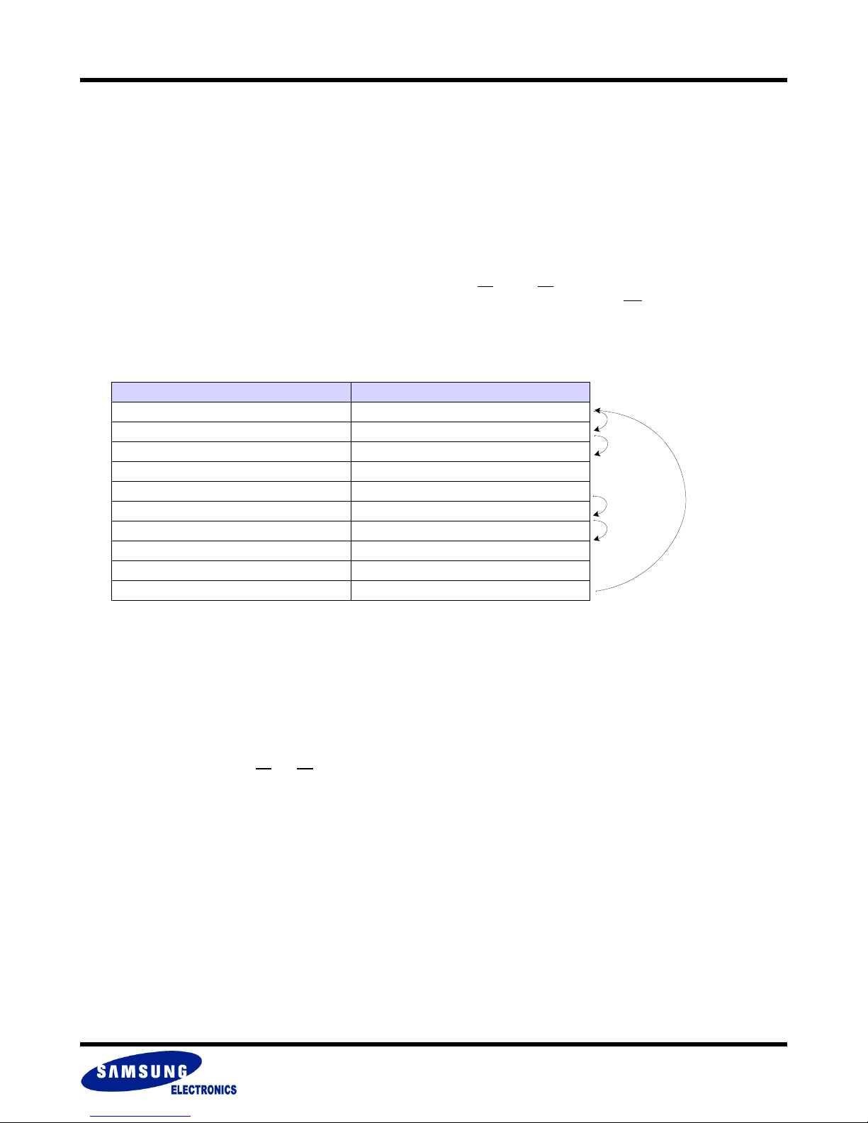
MuxOneNAND2G(KFM2G16Q2A-DEBx)
MuxOneNAND4G(KFN4G16Q2A-DEBx)
3.7.2.1 Continuous Linear Burst Read Operation
See Timing Diagram 6.2
First Clock Cycle
The initial word is output at tIAA after the rising edge of the first CLK cycle. The RDY output indicates the initial word is ready to the system by
pulsing high. If the device is accessed synchronously while it is set to Asynchronous Read Mode, the first data can still be read out.
Subsequent Clock Cycles
Subsequent words are output (Burst Access Time from Valid Clock to Output) tBA after the rising edge of each successive clock cycle, which
automatically increments the internal address counter.
Terminating Burst Read
The device will continue to output sequential burst data until the system asserts CE
ignated address (see Section 2.7.3 for address map information). Alternately, a Cold/Warm/Hot Reset, or a WE
burst read operation.
Synchronous Read Boundary
Division Add.map(word order)
BootRAM Main(0.5KW) 0000h~01FFh
BufferRAM0 Main(1KW) 0200h~05FFh
BufferRAM1 Main(1KW) 0600h~09FFh
Reserved Main 0A00h~7FFFh
BootRAM Spare(16W) 8000H~800Fh
BufferRAM0 Spare(32W) 8010h~802Fh
BufferRAM1 Spare(32W) 8030h~804Fh
Reserved Spare 8050h~8FFFh
Reserved Register 9000h~EFFFh
Register(4KW) F000h~FFFFh
high, or RP low, wrapping around until it reaches the des-
FLASH MEMORY
low pulse will terminate the
Not Support
Not Support
Not Support
Not Support
Not Support
* Reserved area is not available on Synchronous read
3.7.2.2 4-, 8-, 16-, 32-Word Linear Burst Read Operation
See Timing Diagram 6.1
An alternate Burst Read Mode enables a fixed number of words to be read from consecutive address.
The device supports a burst read from consecutive addresses of 4-, 8-, 16-, and 32-words with a linear-wrap around. When the last word in
the burst has been reached, assert CE
In this mode, the start address for the burst read can be any address of the address map with one exception. The device does not support a
32-word linear burst read on the spare area of the BufferRAM.
and OE high to terminate the operation.
- 94 -
Page 95
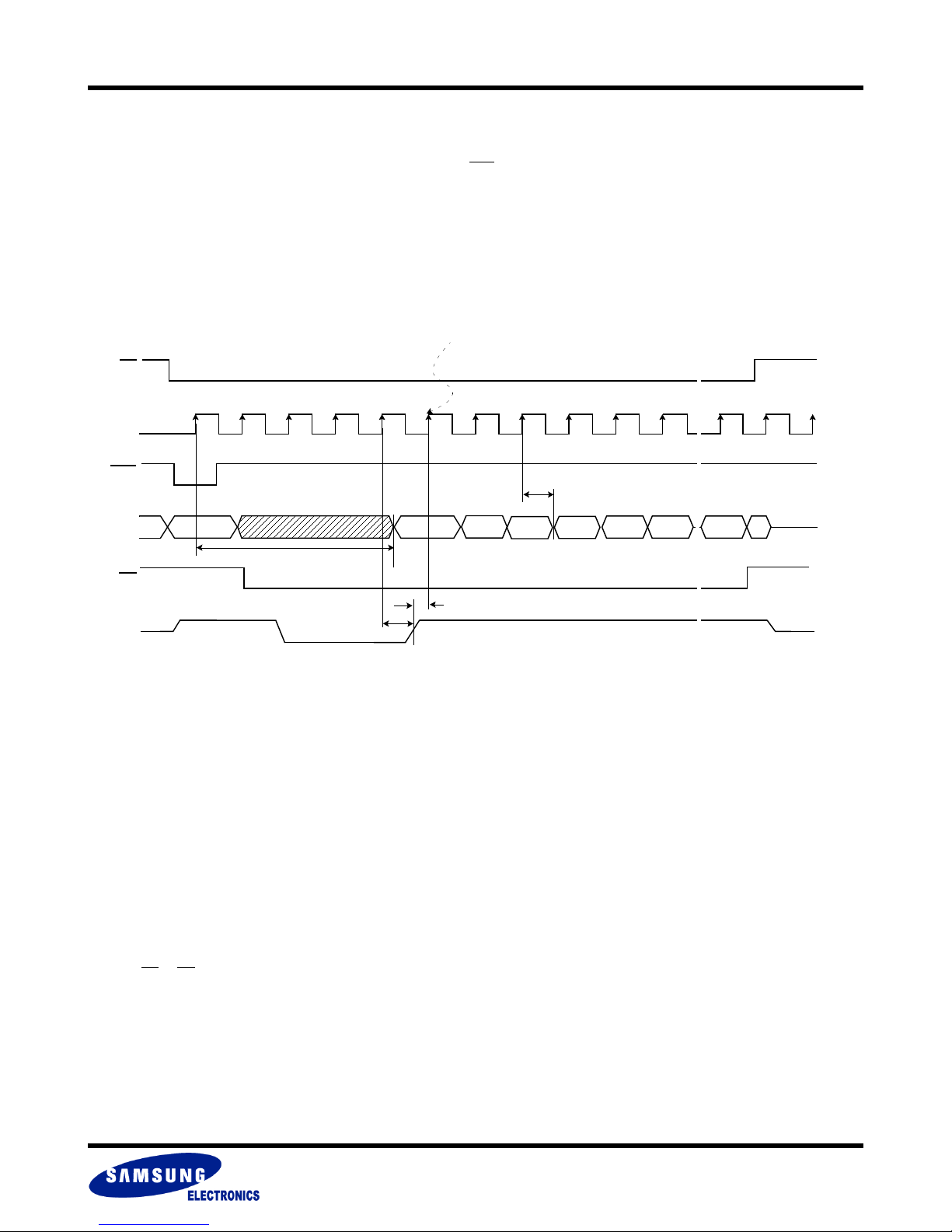
MuxOneNAND2G(KFM2G16Q2A-DEBx)
MuxOneNAND4G(KFN4G16Q2A-DEBx)
3.7.2.3 Programmable Burst Read Latency Operation
See Timing Diagrams 6.1 and 6.2
FLASH MEMORY
Upon power up, the number of initial clock cycles from Valid Address (AVD
The number of clock cycles (n) which are inserted after the clock which is latching the address. The host can read the first data with the
(n+1)th rising edge.
The number of total initial access cycles is programmable from three to seven cycles. After the number of programmed burst clock cycles is
reached, the rising edge of the next clock cycle triggers the next burst data.
Four Clock Burst Read Latency (BRWL=4 case)
CE
CLK
AVD
A/DQ0:
A/DQ15
OE
RDY
Hi-Z
-1 0 1 2 3
Val id
Address
tIAA
tRDYA
4
D6 D7 D0 D1 D2 D3 D7 D0
) to initial data defaults to four clocks.
Rising edge of the clock cycle following last read latency
triggers next burst data
tBA
tRDYS
Hi-Z
*NOTE :
BRWL=4, HF=0 is recommended for 40MHz~66MHz. For frequency over 66MHz, BRWL should be 6 or 7 while HF=1.
Also, for frequency under 40MHz, BRWL can be reduced to 3, and HF=0.
3.7.3 Handshaking Operation
The handshaking feature allows the host system to simply monitor the RDY signal from the device to determine
when the initial word of burst data is ready to be read.
To set the number of initial cycles for optimal burst mode, the host should use the programmable burst read latency configuration (see Section
2.8.19, "System Configuration1 Register").
The rising edge of RDY which is derived at the same cycle of data fetch clock indicates the initial word of valid burst data.
3.7.4 Output Disable Mode Operation
When the CE or OE input is at VIH, output from the device is disabled.
The outputs are placed in the high impedance state.
- 95 -
Page 96
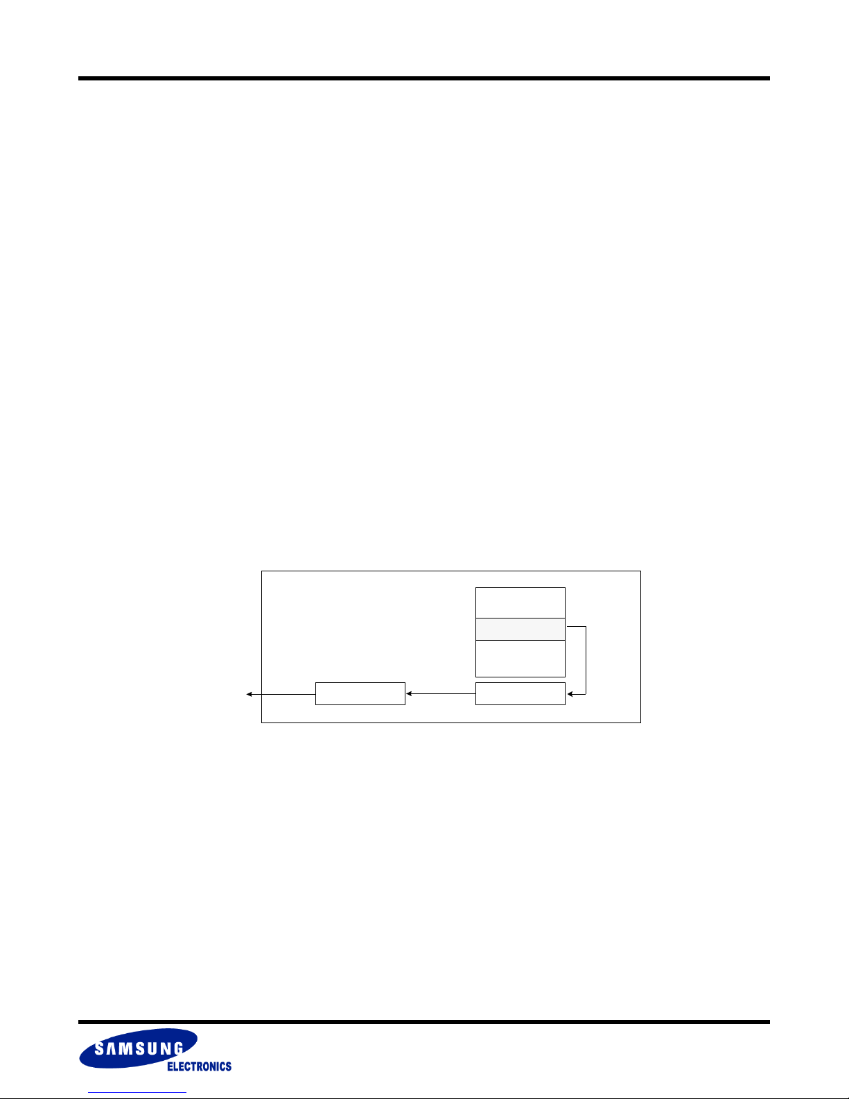
MuxOneNAND2G(KFM2G16Q2A-DEBx)
MuxOneNAND4G(KFN4G16Q2A-DEBx)
3.8 Cache Read Operation (RM=X, WM=X)
A Normal Load Operation(0000h) consists of sequential operation of ‘sensing from NAND Flash Array to Page Buffer’ and ‘transferring from
Page Buffer to DataRAM’.
Cache Read is a method of improving the data read throughput performance of the device by allowing new data to be transferred from the
NAND Flash Array memory into a Page Buffer while the previous data that was requested is transferred from the Page Buffer to the DataRAM.
This method is called Transfer-While Sensing Operation.
This ability to simultaneously sense a new page shortens the read cycle resulting in performance increase to 108Mbytes/second.
Cache Read Mode is designed to continuously read massive data from random address at a high speed.
The characteristics of Cache read is as follows;
-Before entering ‘First Cache Read Command(000Eh)’, address of two pages which will be read will be set on address registers. The register
information follows on next line.
-Register used for first page is Copy-back registers (FCBA, FCPA and FCSA). and the registers used for addressing second page and following cache read are normal address registers(FBA, FPA and FSA). At Cache Read Operation, FCSA and FSA must be set to "00".
-BSA setting is only required once at ‘First Cache Read’ cycle. From the following cycles, BSA will be automatically switched to select
DataRAM0 and DataRAM1 alternately.
-BSC must be fixed as "00"
-To eliminate performance degradation during Ready state(INT high state) due to register setting time, setting registers (FBA, FPA and FSA)
during busy state(INT low state) is possible from third address setting onwards.
-Inputting other commands, which is not related to Cache Read, between ‘First Cache Read Command’ and ‘Finish Cache Read Command’
will fail the Cache Read operation.
-In case of performing Cache Read at INT auto mode, INT low setting is not necessary. INT will automatically go to low when Cache Read
command is issued.
-If host changes DBS or DFS to access the other chip for DDP while performing cache read operation, it will fail the cache read operation.
FLASH MEMORY
Transfer-While Sensing Operation
2) Read
Host
A Cache-Read flow chart is on the following page.
DataRAM
NAND Flash
Array
Selected Page
1) Sensing
1) Transfer
Page Buffer
- 96 -
Page 97
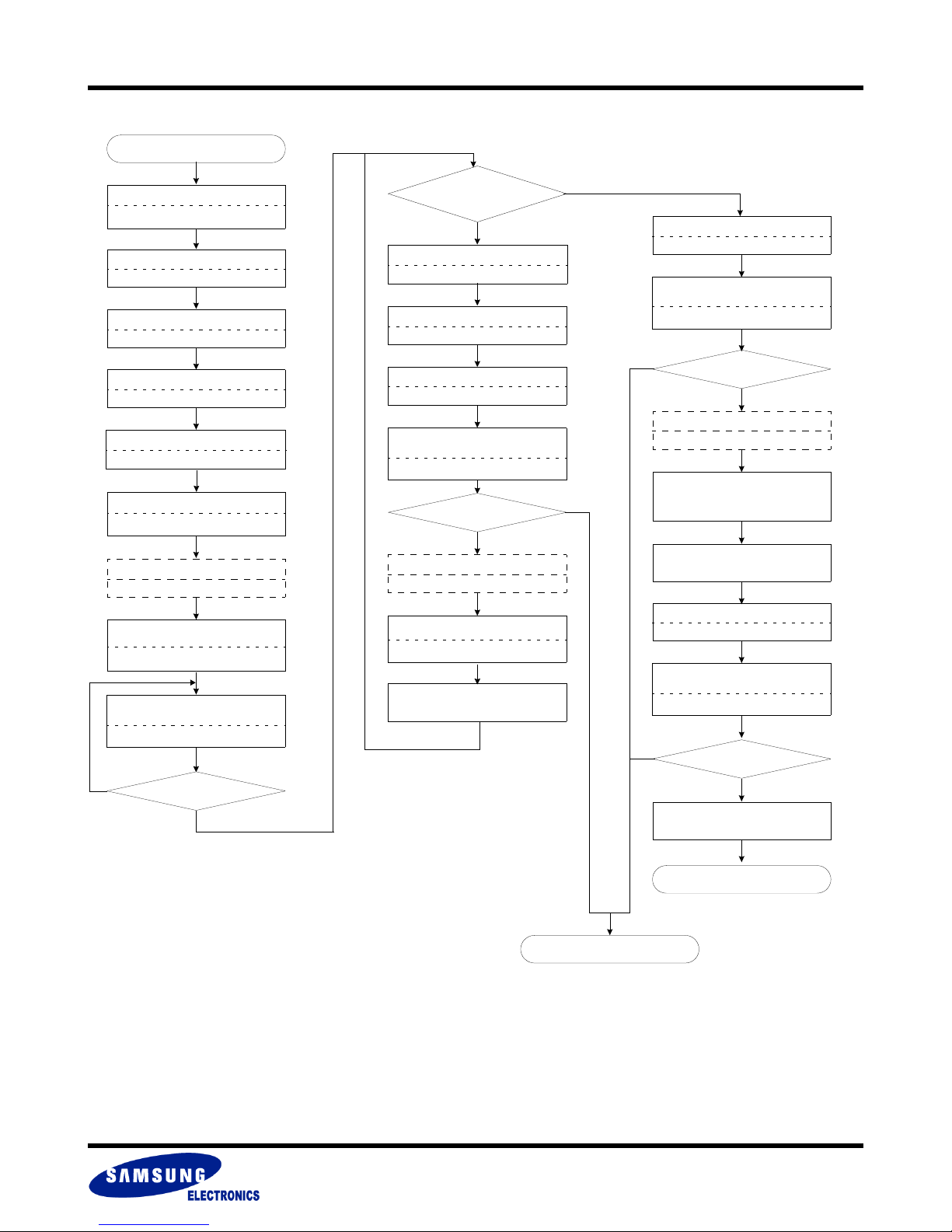
MuxOneNAND2G(KFM2G16Q2A-DEBx)
MuxOneNAND4G(KFN4G16Q2A-DEBx)
Cache Read Flow Chart
Start
FLASH MEMORY
Select DataRAM for DDP
Add: F101h DQ=DBS
Write ‘BSA1), BSC2)’ of Flash
Add: F200h DQ=BSA, BSC
Write ‘FCBA’ of Flash
Add: F102h DQ=FCBA
Write ‘FCPA, FCSA2)’ of Flash
Add: F103h DQ=FCPA, FCSA
Write ’DFS*, FBA’ of Flash
Add: F100h DQ=DFS, FBA
Write ‘FPA, FSA2)’ of Flash
Add: F107h DQ=FPA, FSA
Write 0 to Interrupt register
Add: F241h DQ=0000h
Write ‘Cache Read’ Command
Add: F220h DQ=000Eh
Read Controller Status
Register Add: F240h
DQ[15]=Ongo & DQ[13]=Load
No
DQ[15]=1 & DQ[13]=1 ?
Yes
3)
Done with
(n-1)th command
issue?
No
Write ’DFS*, FBA’ of Flash
Yes
Wait for INT high State
3)
Add: F241h DQ[15]=INT
Add: F100h DQ=DFS, FBA
Read Controller Status
Register
Write ‘FPA, FSA2)’ of Flash
3)
Add: F240h DQ[10]=Error
Add: F107h DQ=FPA, FSA
Wait for INT high State
Add: F241h DQ[15]=INT
Read Controller Status
Register
No
Write 0 to Interrupt register
DQ[10]=0?
Yes
4)
Add: F241h DQ=0000h
Add: F240h DQ[10]=Error
Write ‘Finish Cache Read
Command’ @ Final Read
Add: F220h DQ=000Ch
DQ[10]=0?
No
Yes
4)
Write 0 to Interrupt register
4)
Add: F241h DQ=0000h
Write ‘Cache Read’ Command
Host reads data from
DataRAM
6)
Wait for INT high State
Add: F241h DQ[15]=INT
Add: F220h DQ=000Eh
Read Controller Status
Host reads data from
DataRAM
5)
Add: F240h DQ[10]=Error
Register
No
DQ[10]=0?
Yes
Host reads data from
DataRAM
* DBS, DFS is for DDP
(DFS must be same)
NOTE :
1) In case of first cycle cache read, BSA must be set to 1000 or 1100, and from second cycle cache read,
BSA will automatically be switched between DataRAM0 and DataRAM1.
2) BSC, FSA and FCSA must be set to "00".
3) These steps can also be set during INT=High, before next ’Cache Read Command’.
4) ’Write 0 to interrupt register’ step may be ignored when using INT auto mode. Refer to chapter 2.8.18.1
5) When host reads data from DataRAM, host should start from the DataRAM of the first set BSA, and then next DataRAM alternately, as the number of Cache
Read.
END
Map out
- 97 -
Page 98
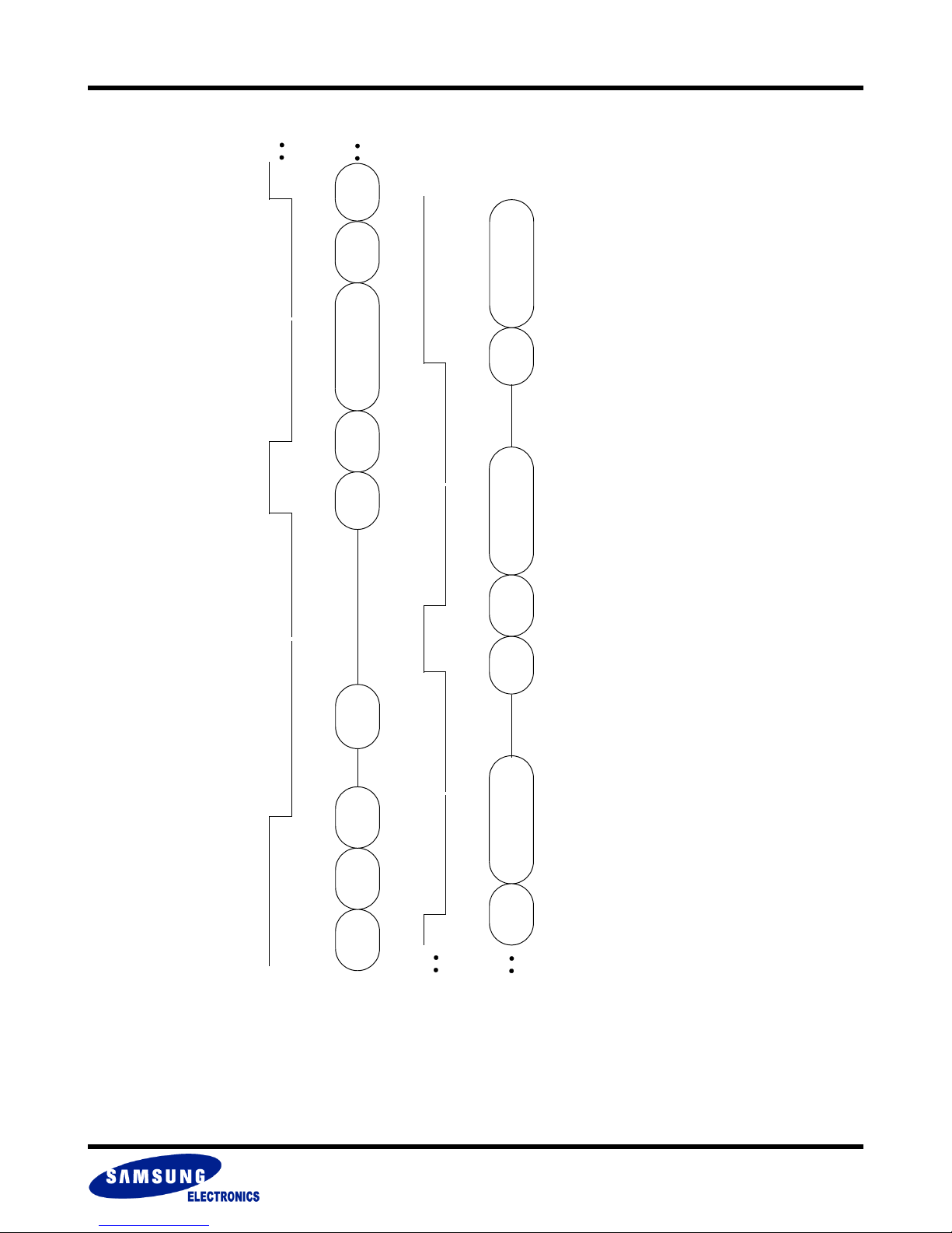
MuxOneNAND2G(KFM2G16Q2A-DEBx)
MuxOneNAND4G(KFN4G16Q2A-DEBx)
Cache Read Diagram
Read
Status
4th
Setting
Address
Host reads 1st
data from DataRAM
Setting
Command
FLASH MEMORY
Host reads nth
data from DataRAM
Read
Status
Read
Status
Host reads (n-1)th
data from DataRAM
Finish
Setting
Status
Host reads (n-2)th
Command
Command
Read
data from DataRAM
Setting
-Host read 1st~nth data from DataRAM : During this step, Host can read data from DataRAM by any read mode which supported by MuxOneNAND.
-Finish Command Setting : If host want to finish Cache Read, Host can finish Cache Read by issuing Finish Command.
-Controller Status Register Status: During Cache Read - Ongoing / Load
ECC Error during Cache Read - Ongoing / Load / Error
-1st Address Setting : Address Setting Operation for first page load(FCBA, FCPA, FCSA, and BSA).
-2nd~nth Address Setting : Address Setting Operation from 2nd~nth page load(FBA and FPA).
-Command Setting : It consists of writing 0 to Interrupt register and writing command to Command register. (In INT auto mode, writing 0 to Interrupt register may be ignored) -Status Read : It consists of INT high state checking and Controller Status Register checking step.
ECC Error at Finish Cache Read - Load / Error
NOTE :
1) 3rd~nth address can be set during INT=low, and also during INT=High, before next ‘Cache Read Command’.
1)
3rd
Setting
Address
Setting
Command
2nd
Setting
Address
1st
Setting
Address
INT
INT
A/DQ0:
A/DQ15
(cont.)
- 98 -
A/DQ0:
A/DQ15
(cont.)
Page 99
MuxOneNAND2G(KFM2G16Q2A-DEBx)
MuxOneNAND4G(KFN4G16Q2A-DEBx)
3.9 Synchronous Burst Block Read Operation(RM=1, WM=X)
See Timing Diagram 6.3 and 6.4.
MuxOneNAND is internally composed of two DataRAMs and NAND Flash Array. And for host to read data from NAND Cell Array, load
operation which moves data from NAND Cell Array to DataRAM is required. After this load operation, host may use various read mode, such
as synchronous burst read or asynchronous read, to read data from MuxOneNAND.
But these types of read mode require issuing of address and Load Command for each page, and CPU had the burden of calculating address
to be read. To solve this burden, Synchronous Burst Block Read Mode is introduced, which enables host to read the data of succeeding page
with CLK toggle, after initial address setting and command input. This Synchronous Burst Block Read is intended to transfer continuous massive data in NAND Flash Array at high speed, and it sequentially reads out data only from Main Area, where large sized data is stored.
The addresses set for Synchronous Burst Block Read is Start Page Address(FPA), Number of Page(FPC) and BSA. Note that the number of
page set by FPC should not exceed the block boundary, since page wrap-around is not supported. And from the start page address to desired
number of page, Synchronous Burst Block Read will output data by CLK toggle and CE
64pages. (Refer to 2.8.13)
The Host can access MuxOneNAND during Synchronous Burst Block Read in between every 1-page of read cycle. When host accesses DataRAMs, the start address of DataRAMs must be a multiple of 4. In doing this, INT pin or bit is used as indicator signal. Thus, before host reads
1-page data from DataRAM, host must confirm INT pin or bit return low to high, and then enable CE
read operation for this 1-page is done, INT will automatically turn low. Note that INT auto mode is a mandatory option for Synchronous Burst
Block Read, and WE
Therefore, the steps are as follows;
1. Host will deassert CE
2. And then assert the CE
3. Then disable this other device by deasserting CE
4. Once the host confirms the INT pin or bit of MuxOneNAND turn low to high, host may read the data of following page by asserting CE
to synchronous burst block read operation timing).
must always be set high throughout this operation.
of MuxOneNAND after checking the indicator(INT pin / bit) turn low.
of other device to perform another operation.
when desired operation is done.
enable/disable. FPC must be set from 3pages to
to read 1-page of data. And when host
FLASH MEMORY
(refer
Return of INT pin to high implies the internal load operation from NAND Flash Array to DataRAM is complete. Also, even when the host is
NOT accessing other device, this assert/deassert of CE
To read data from this loaded 1 page, same 4, 8, 16, 32, continuous (1K word) linear burst read operation of synchronous burst read may be
utilized.
In conclusion, by supporting indicator signal such as INT pin or bit, host may access other device without terminating continuous linear synchronous burst block read, while using continuous linear burst read mode as synchronous block read within 1 block between every (n) page
and (n+1) page. (refer to synchronous burst block read boundary)
For 1 bit error during Synchronous Burst Block Read, ECC correction will be done automatically, and Controller Status Register(F240h) will
show ‘load ok’ status. On the other hand, for 2 bit error during Synchronous Burst Block Read, ECC correction is not possible, and Controller
Status Register(F240h) will show ‘load fail’ status.
Note that for both cases, ECC Status Register(FF00h) value will remain the same at value of 0000h.
step is necessary.
- 99 -
Page 100
MuxOneNAND2G(KFM2G16Q2A-DEBx)
MuxOneNAND4G(KFN4G16Q2A-DEBx)
3.9.1 Burst Address Sequence During Synchronous Burst Block Read Mode
In a Synchronous Burst Block Read, data is output with respect to a clock input.
MuxOneNAND is capable of a continuous linear burst operation within one block size and a fixed-length linear burst operation of a preset
length.
Note that only INT pin is valid indicator signal for continuous linear burst read operation but both INT pin and bit are valid for a fixed-length linear burst operation.
Same as the normal burst mode, the initial word will be output asynchronously, regardless of BRWL While the following words will be determined by BRWL value.
The latency is determined by the host based on the BRWL bit setting in the System Configuration 1 Register. The default BRWL is 4 latency
cycles. At clock frequencies of 40MHz or lower, latency cycles can be reduced to 3, at frequency range from 40MHz to 66MHz, latency cycle
should be over 4. And at 83MHz frequency, BRWL should be set to 6. BRWL can be set up to 7 latency cycles.
FLASH MEMORY
The BRWL registers can be read during a burst read mode by using the AVD
signal with an address.
3.9.2 Continuous Linear Burst Read Operation During Synchronous Burst Block Read Mode
First Clock Cycle
The initial word is output at tIAA after the rising edge of the first CLK cycle. The RDY output indicates the initial word is ready to the system by
pulsing high. If the device is accessed synchronously while it is set to Asynchronous Read Mode, the first data can still be read out.
Subsequent Clock Cycles
Subsequent words are output (Burst Access Time from Valid Clock to Output) tBA after the rising edge of each successive clock cycle, which
automatically increments the internal address counter.
Terminating Synchronous Burst Block Read
The device will continue to output sequential burst data until the system resets (Cold/Warm/Hot Reset), wrapping around until it reaches the
designated address (see Section 3.9.1 for burst address sequence). Asserting WE
operation.
low is prohibited during Synchronous Burst Block Read
- 100 -
 Loading...