

SAMSUNG MM26LC Service Manual
©
Samsung Electronics Co., Ltd. Sep. 1996. Code No. AH68-20129A
MICRO COMPONENT SYSTEM
1. Precautions
2. Specifications
3. Disassembly and Reassembly
4. Alignment and Adjustments
5. Special Circuit Descriptions
6. Troubleshooting
7. Exploded Views and Parts List
8. Electrical Parts List
9. Block Diagrams
10. PCB Diagrams
11. Wiring Diagram
12. Schematic Diagrams
VOLUME
BAND
MUTE
EQ
PRESET
PUSH
EJECT
SRS
ON/STANDBY
TUNING
COUNTER
REC/STOP
POWER
TUNER
CD
TAPE
AUX
PHONES
SRS
SERVICE
Manual
MICRO COMPONENT
SYSTEM
MM-26
CONTENTS
1. Precautions
Follow these safety, servicing and ESD precautions to prevent damage and protect against potential hazards
such as electrical shock and X-rays.
1-1 Safety Precautions
1. Be sure that all of the built-in protective
devices are replaced.
(Reading should
2. When reinstalling the chassis and its
assemblies, be sure to restore all protective
devices, including control knobs and
compartment covers.
3. Make sure that there are no cabinet
openings through which people-particularly children--might insert fingers
and contact dangerous voltages. Such
openings include the spacing between the
picture tube and the cabinet mask,
excessively wide cabinet ventilation slots,
and improperly fitted back covers.
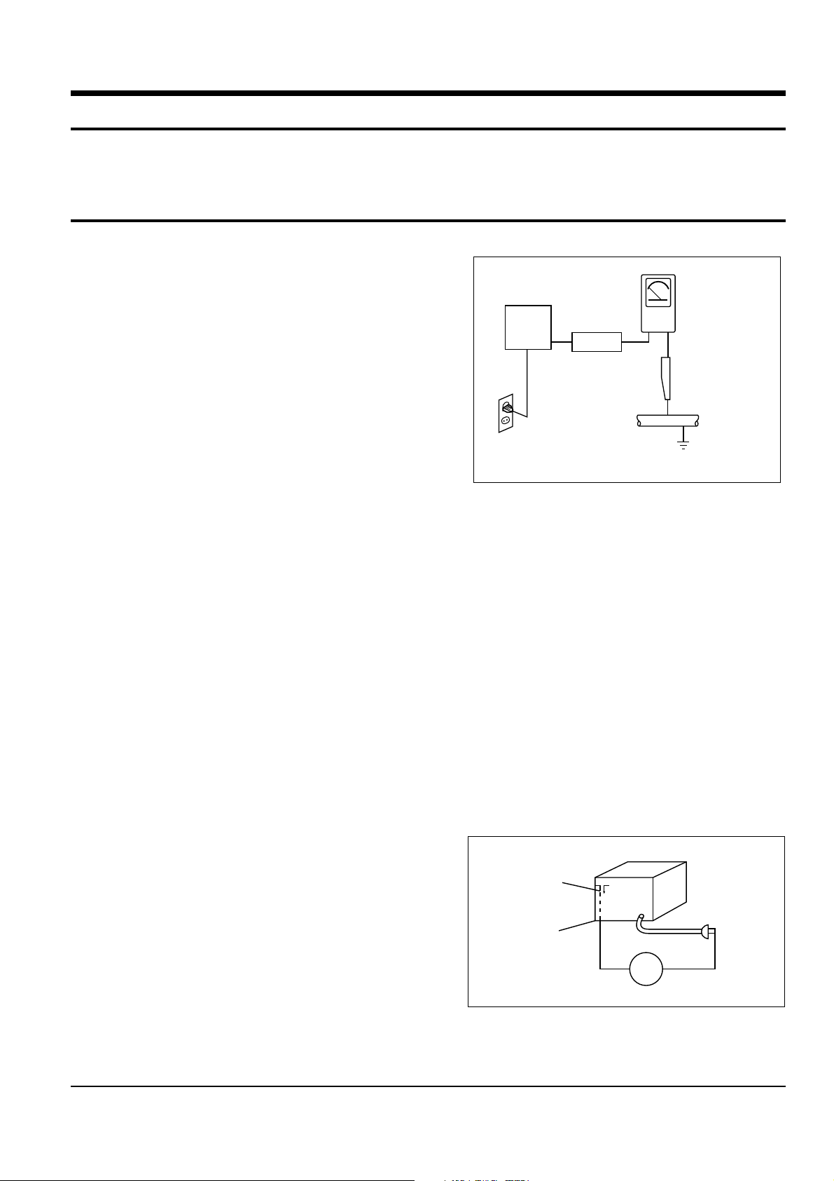
Device
Under
Test
Test all
exposed metal
surfaces
2-Wire Cord
Also test with
plug reversed
(using AC adapter
plug as required)
Fig. 1-1 AC Leakage Test
not be above
0.5mA)
Leakage
Currant
Tester
Earth
Ground
4. Design Alteration Warning:
Never alter or add to the mechanical or
electrical design of the unit. Example: Do
not add auxiliary audio or video connectors. Such alterations might create a safety
hazard. Also, any design changes or additions will void the manufacturer's warranty.
5. Leakage Current Hot Check (Figure 1-1):
Warning: Do not use an isolation
transformer during this test. Use a leakagecurrent tester or a metering system that
complies with American National Standards
Institute (ANSI C101.1, Leakage Current for
Appliances), and Underwriters Laboratories
(UL Publication UL1410, 59.7).
With the unit completely reassembled, plug
the AC line cord directly into a 120V AC
outlet. With the unit's AC switch first in
the ON position and then OFF, measure the
current between a known earth ground
(metal water pipe, etc.) and all exposed
metal parts. Examples: Handle brackets,
metal cabinets, screwheads and control
shafts. The current measured should not
exceed 0.5 milliamp. Reverse the powerplug prongs in the AC outlet and repeat.
6. Insulation Resistance Cold Check:
(1) With the unit's AC plug disconnected
from the AC source, connect an electrical
jumper across the two AC prongs. (2) Set
the power switch to ON. (3) Measure the
resistance between the shorted AC plug and
any exposed metallic parts. Example:
Screwheads, antenna, control shafts or
handle brackets.
If any of the exposed metallic parts has a
return path to the chassis, the measured
resistance should be between 1 and 5.2
megohms. If there is no return path, the
measured resistance should be "infinite." If
the resistance is outside these limits, a shock
hazard might exist. See Figure 1-2
Antenna
Terminal
Exposed
Metal Part
ohm
Ohmmeter
Fig. 1-2 Insulation Resistance Test
Samsung Electronics 1-1

Precautions
1-1 Safety Precautions (Continued)
7. Components, parts and wiring that appear
to have overheated or that are otherwise
damaged should be replaced with parts
that meet the original specifications.
Always determine the cause of damage or
overheating, and correct any potential
hazards
8. Observe the original lead dress, especially
near the following areas: Antenna
wiring, sharp edges, and especially the
AC and high voltage power supplies.
Always inspect for pinched, out-of-place,
or frayed wiring. Do not change the
spacing between components and the
printed circuit board. Check the AC
power cord for damage. Make sure that
no wires or components touch thermally
hot parts.
1-2 Servicing Precautions
9. Product Safety Notice:
Some electrical and mechanical parts
have special safety-related characteristics
which might not be obvious from visual
inspection. These safety features and the
protection they give might be lost if the
replacement component differs from the
original--even if the replacement is rated
for higher voltage, wattage, etc.
10 Components that are critical for safety are
indicated in the circuit diagram by
shading, or . Use replacement
components that have the same ratings,
especially for flame resistance and
dielectric strength specifications. A
replacement part that does not have the
same safety characteristics as the original
might create shock, fire or other hazards.
Warning1: First read the "Safety Precautions" section of this manual. If some unforeseen circumstance creates a conflict
between the servicing and safety precautions, always follow the safety precautions.
1. Servicing precautions are printed on the
cabinet. Follow them.
2. Always unplug the unit's AC power cord
from the AC power source before
attempting to: (a) Remove or reinstall any
component or assembly, (b) Disconnect an
electrical plug or connector, (c) Connect a
test component in parallel with an
electrolytic capacitor.
3. Some components are raised above the
printed circuit board for safety. An
insulation tube or tape is sometimes used.
The internal wiring may be clamped to
prevent contact with thermally hot
components. Reinstall all such elements to
their original position.
4. After servicing, always check that the
screws, components and wiring have been
correctly reinstalled. Make sure that the
portion around the serviced part has not
been damaged.
5. Check the insulation between the blades of
the AC plug and accessible conductive parts
(examples: metal panels, input terminals
and earphone jacks).
6. Insulation Checking Procedure: Disconnect
the power cord from the AC source and
turn the power switch ON. Connect an
insulation resistance meter (500V) to the
blades of the AC plug.
The insulation resistance between each
blade of the AC plug and accessible
conductive parts (see above) should be
greater than 1 megohm.
7. Never defeat any of the B+ voltage
interlocks. Do not apply AC power to the
unit (or any of its assemblies) unless all
solid-state heat sinks are correctly installed.
8. Always connect a test instrument's ground
lead to the instrument chassis ground
before connecting the positive lead; always
remove the instrument's ground lead last.
Samsung Electronics1-2
1-3 Precautions for Electrostatically Sensitive Devices (ESDs)
Precautions
1. Some semiconductor ("solid state") devices
are easily damaged by static electricity.
Such components are called Electrostatically
Sensitive Devices (ESDs). Examples include
integrated circuits and some field-effect
transistors. The following techniques will
reduce the occurrence of component
damage caused by static electricity.
2. Immediately before handling any
semiconductor components or assemblies,
drain the electrostatic charge from your
body by touching a known earth ground.
Alternatively, wear a discharging
wrist-strap device. (Be sure to remove it
prior to applying power--this is an electric
shock precaution.)
3. After removing an ESD-equipped assembly,
place it on a conductive surface such as
aluminum foil to prevent accumulation of
electrostatic charge.
4. Do not use freon-propelled chemicals.
These can generate electrical charges that
damage ESDs.
5. Use only a grounded-tip soldering iron
when soldering or unsoldering ESDs.
6. Use only an anti-static solder removal
device. Many solder removal devices are
not rated as "anti-static" (these can
accumulate sufficient electrical charge to
damage ESDs).
7. Do not remove a replacement ESD from its
protective package until you are ready to
install it. Most replacement ESDs are
packaged with leads that are electrically
shorted together by conductive foam,
aluminum foil or other conductive
materials.
8. Immediately before removing the protective
material from the leads of a replacement
ESD, touch the protective material to the
chassis or circuit assembly into which the
device will be installed.
9. Minimize body motions when handing
unpackaged replacement ESDs. Motions
such as brushing clothes together, or lifting
a foot from a carpeted floor can generate
enough static electricity to damage an ESD.
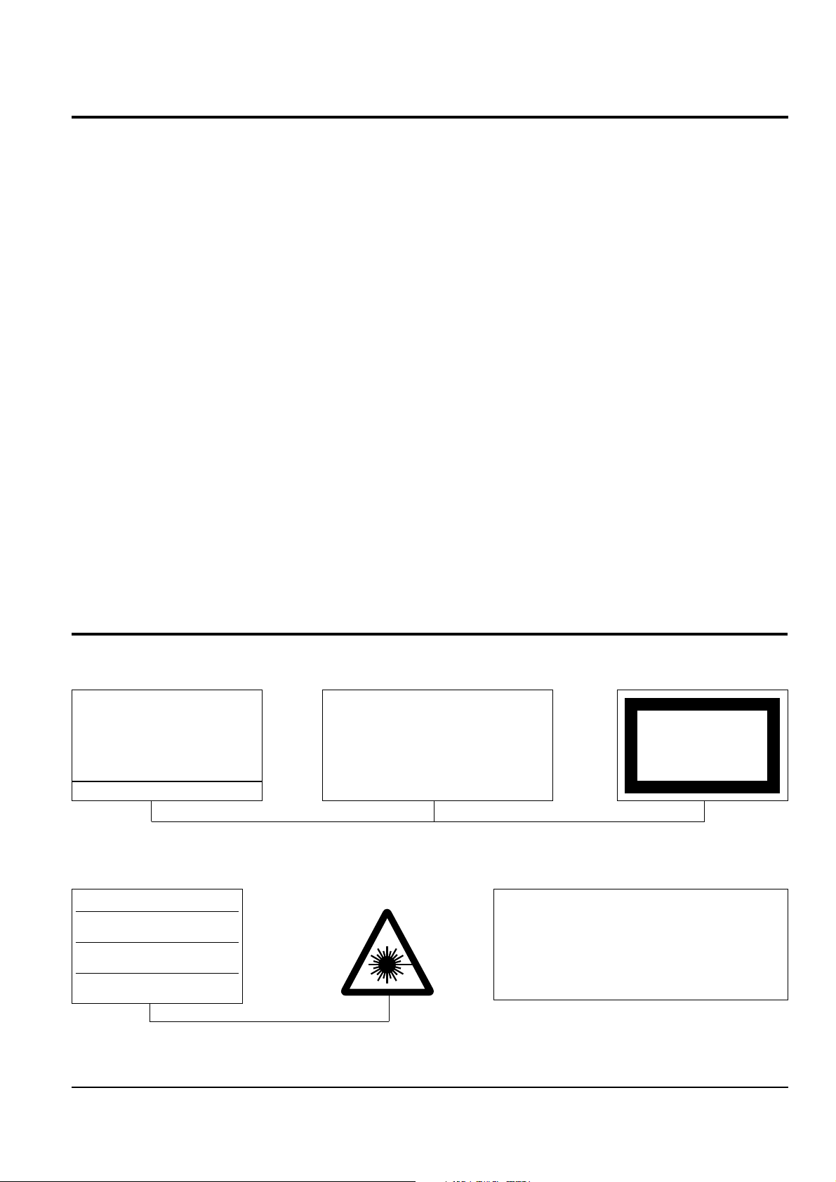
1-4 Special Precautions and Warning Labels for Laser Products
(UL)
This Product Complies with
DHHS Rules 21CFR, Sub
chapter J.At date of Manufacture
(SCAN)
CAUTION : INVISIBLE LASER RADIATION WHEN OPEN
AND INTERLOCKS DEFEATEO AVOIDEXPOSURE TO BEAM
ADVARSEL:USYNLIG LASERSTRÅLING VED ABNING
NÅR SIKKERHEDSAFBRYDERE ER UDE AF FUNKTION
UNDGA UDSAETTELSE FOR STRALING
VARO:AVATTAESSA JA SUOJALUKITUS OHITETTAESSA
OLET ALTTINA NAKYMATTÖMALLE LASERSATEILYLLE ALA
KATSO SATEESEEN!
VARNING:OSYNLIG LASERSTRÅLNING NAR DENNA DEL
AR OPPNAD OCH SPARREN AR URKOPPLAD BETRAKTA
EJSTRÅLEN!
CERTIFIED ONLY TO CANADIAN
ELECTRICAL CODE.
CERTIFIE EN VERTU DU CODE
CANADIAN DE LELETRICITE
SEULEMENT
Fig. 1-3 Warning Labels (Location: Enclosure Block)
(EU)
(CSA)
UL : Manufactured for U.S.A. Market.
CSA : Manufactured for Canadian Market.
EU : Manufactured for European Market.
SCAN : Manufactured for Scandinavian
Market.
(EU)
CLASS 1
LASER PRODUCT
Fig. 1-4 Warning Labels (Location: Disc Clamper, Inner Side of Unit Door or Nearby Unit Chassis )
Samsung Electronics 1-3
Precautions
1-4 Special Precautions and Warning Labels for Laser Products (Continued)
1-4-1 Warnings
1. When servicing, do not approach the LASER
exit with the eye too closely. In case it is
necessary to confirm LASER beam emission,
be sure to observe from a distance of more
than 30 cm from the surface of the objective
lens on the optical pick-up block.
2. Do not attempt to handle the objective lens
when the DISC is not on the tray.
1-4-2 Laser Diode Specifications
Material: GaAs+ GaAlAs
Wavelength: 760-800 nm
Emission Duration: Continuous
Laser Output: 0.2 mw (measured at a
1.6 mm distance from the objective lens
surface on the optical pick-up block.)
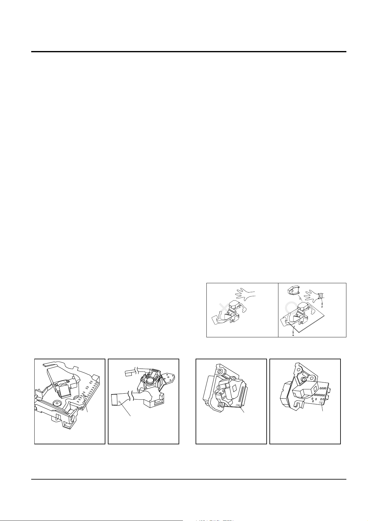
1-4-3 Handling the Optical Pick-up
1. Static electricity from clothing or the body
may cause electrostatic breakdown of the
laser diode in the Optical Pickup. Follow
this procedure:
2. Place a conductive sheet on the work bench
(i.e., the black sheet used for wrapping
repair parts.) Note: The surface of the work
bench should be covered by a copper
ground plane, which is grounded.
3. The repair technician must wear a wrist
strap which is grounded to the copper sheet.
4. To remove the Optical Pickup block:
Place the set on the conductive sheet, and
momentarily touch the conductive sheet
with both hands. (While working, do not
allow any electrostatic sources--such as
clothes--to touch the unit.)
5. Ground the "Short Terminal" (located on the
PCB, inside the Pickup Assembly) before
replacing the Pickup. This terminal should
be shorted whenever the Pickup Assembly
is lifted or moved.
short
terminal
SOH91VI(LDP)
short terminal
SOH91CI(CAR,walkman)
6. After replacing the Pickup, reopen the Short
Terminal. See diagrams below:
1M
THE UNIT
(1) WRIST-STRAP
FOR GROUNDING
short
terminal
SOH-A1
(CMS-V10,CMS-V30)
1M
SOH94T4N
(CMS-V10,CMS-V30)
CONDUCTIVE SHEET
short
terminal
Samsung Electronics1-4
Power source
Power consumption
Dimensions (mm)
AC 230V 50Hz (Option)
90W
162(W)x280(H)x278(D)
Power output
Total harmonic distortion
Frequency range
Signal to noise ratio
Channel separation
Frequency range
Usable sensitivity
Signal to noise ratio
IF rejection ratio
Total harmonic distoration
Separation (Stereo)
Frequency range
Usable sensitivity
Signal to noise ratio
IF rejection ratio
Total harmonic distoration
Frequency range
Usable sensivity
Signal to noise ratio
Frequecny range
WOW FLUTTER
Erasing effect
Signal to noise ratio
Total harmonic distortion
Frequency response
Signal to noise ratio
Channel separation
Total harmonic distortion
87.5 ~ 108MHz
10dB
50dB
60dB
1.5%
25dB
522 ~ 1611KHz
50dB
40dB
33dB
2%
146 ~ 290KHz
60dB
33dB
125Hz ~ 8KHz
0.2%
50dB
40dB
2.5%
100Hz ~ 10KHz(¡ 1dB)
85dB(1kHz 0dB)
75dB(1kHz 0dB)
0.1%(1kHz 0dB)
12.5W/CH
0.5%
50Hz ~ 30KHz
70dB
40dB
General
Amp
Tuner
Cassette
Compact Disc
FM
MW
LW
Samsung Electronics 2-1
* Specifications are subject to change without notice.
2. Specifications
3. Disassembly and Reassembly
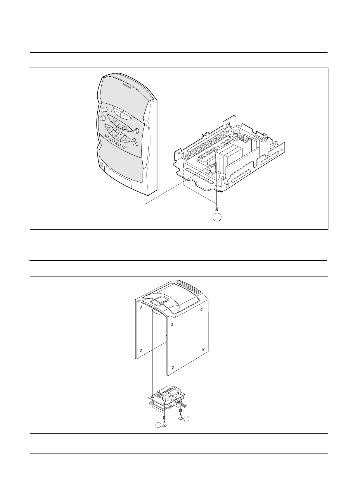
3-1 Cabinet-Top, Cabinet-Rear
1. Remove 8 screws of ! and 6 screws of @ of its rear part.
2. Pull its top part upward vertically as shown in the figure 3-1.
1
1
1
1
2
2
2
2
2
Samsung Electronics 3-1
Figure 3-1
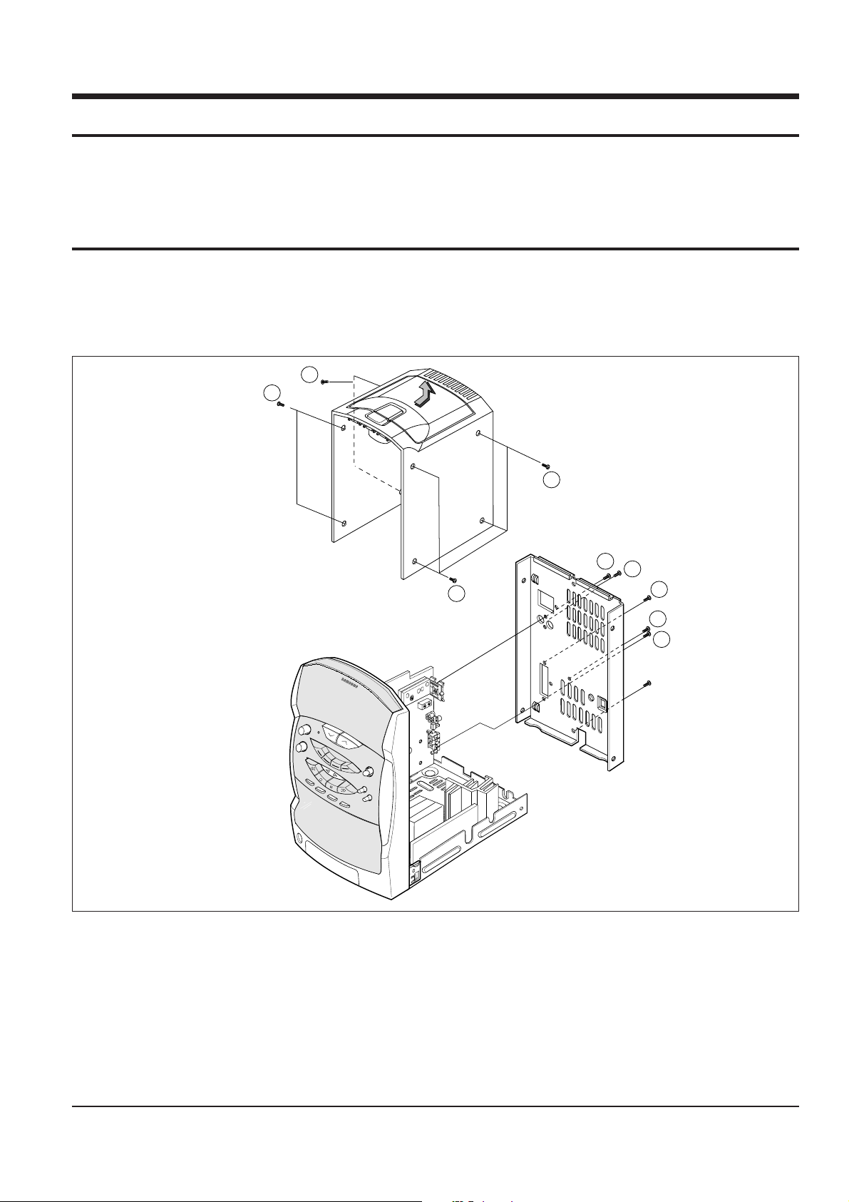
3-2 Main-PCB
1. Remove the Main-PCB backward.
3-2 Samsung Electronics
Main-PCB
Figure 3-2
Disassembly and Reassembly
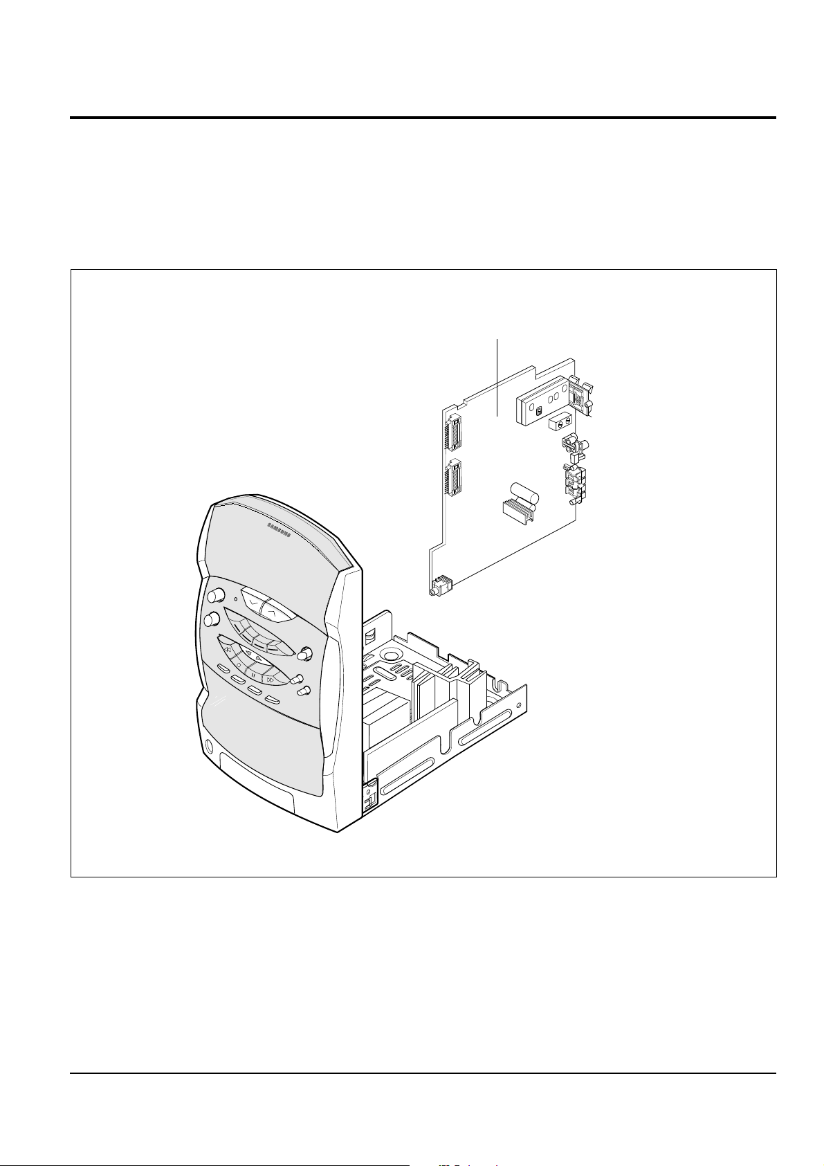
3-4 CD-Pack
1. Undo 4 screws of ! and then remove the CD-Pack downward.
3-3 Cabinet-Bottom
1. Remove 3 screws of ! and pull it out backward.
1
Samsung Electronics 3-3
Figure 3-3
Figure 3-4
1
1
Disassembly and Reassembly
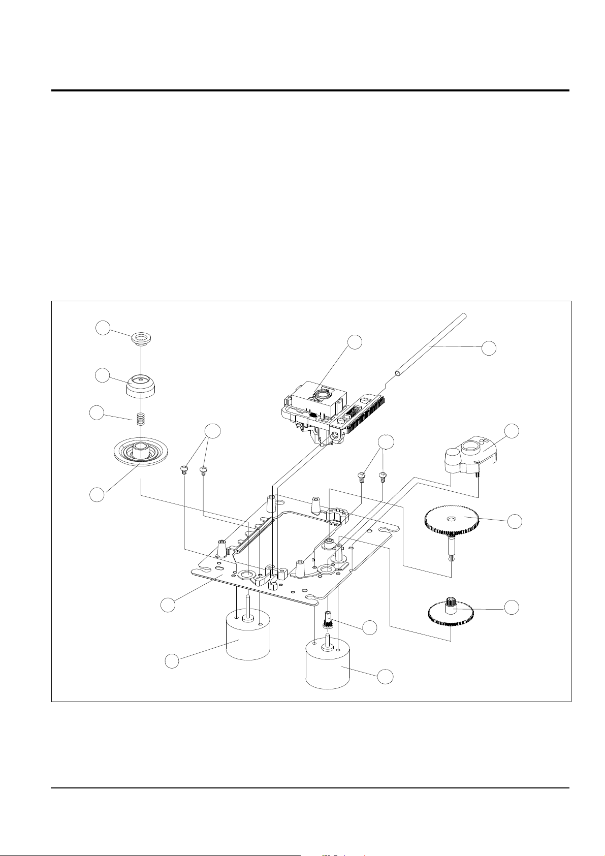
3-5 CD Deck
1. Remove the Shaft ! .
2. Lift the P/U @ .
Note : Take extreme care not to touch the surface of lens.
3. Lift the Center-knob #.
4. Remove the Center-ring $ .
5. Remove the Spring-T/Table % .
6. Remove the Turn-Table (M) ^ .
7. Remove 2 screw & and then remove the Spindle-Motor * .
8. Remove the Cover-Gear ( by pushing the hook.
9. Remove the Gear(c) ) by pushing the hook.
10. Lift the Gear(b) 1 .
11. Remove the Gear(a) 2 .
12. Remove 2 screws 3 and then remove the Feed-Motor 4 .
13. Remove the Chassis-Deck(M) 5.
4
6
7
13
2
1
9
10
11
12
14
15
8
3
5
3-4 Samsung Electronics
Figure 3-5
Disassembly and Reassembly
***
Remark
***
After adjusting the AM, be sure to
adjust the FM.
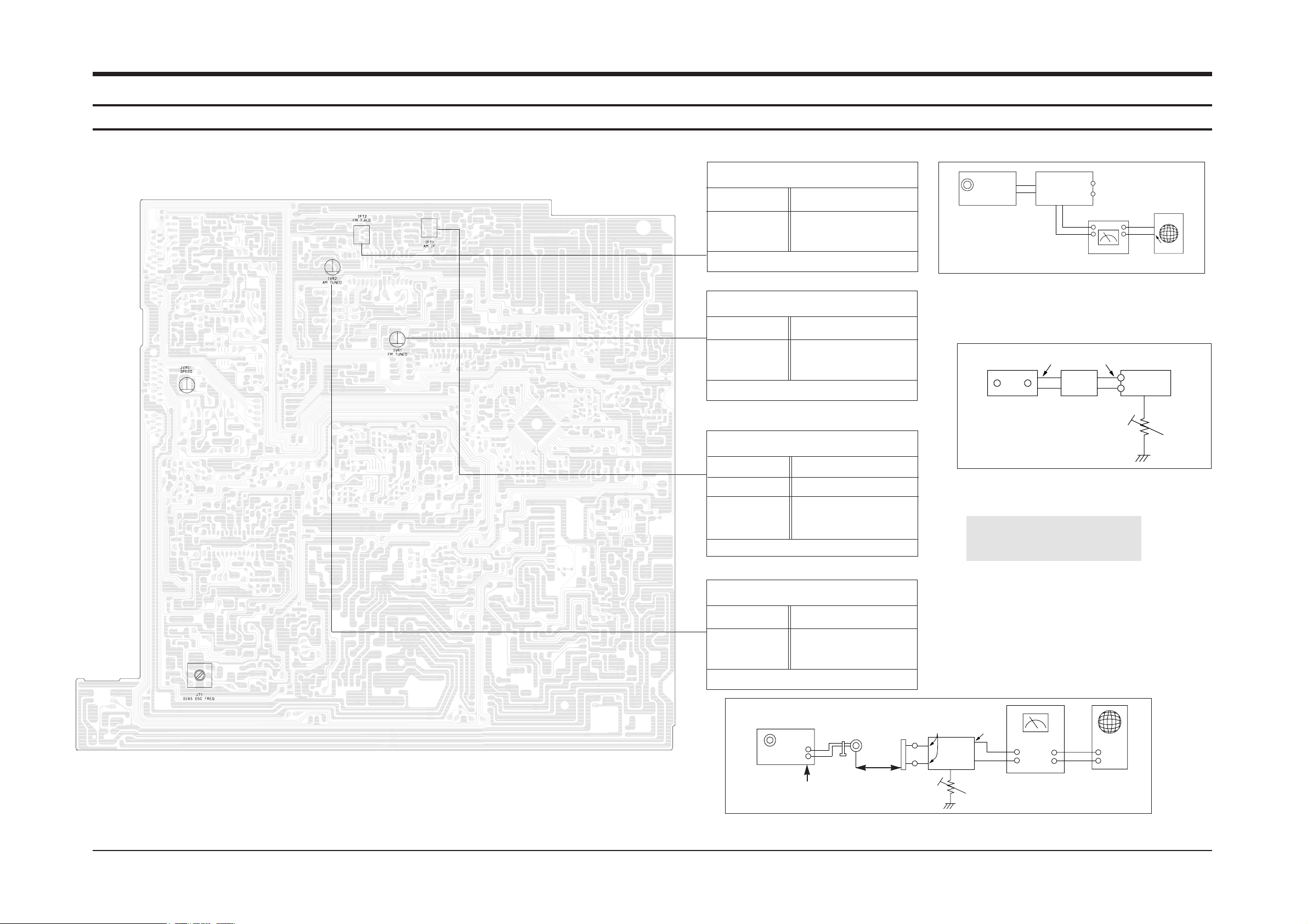
4. Alignment and Adjustments
4-1 Tuner
FM T.H.D Adjustment
SSG FREQ. 98MHz
Adjustment
point FM DETECTOR COIL
(IFT2))
Minumum output(Figure 4-1)
AM Search Level Adjustment
SSG FREQ. 999KHz
Adjustment
point SEMI-VR(20KB)
(ISVR2)
"TUNED" is shown on LCD(Figure 4-3)
AM I.F Adjustment
SSG FREQ. 450KHz
SET FREQ. 522KHz
Adjustment
point AM IF COIL
(IFT1)
"TUNED" is shown on LCD(Figure 4-3)
FM
Antenna
Terminal
Speaker
Terminal
Input
Input
Figure 4-1 IF CENTER and T.H.D Adjustment
Figure 4-3 AM Auto Search Level Adjustment
Output
Distortion Meter
Oscilloscope
FM SSG
AM SSG
52dB
20K
Test Loop
Antenna
GND
20dB
75Ω
Dummy
FM IN
FM Antenna
SET
5 kB
SET
Output
GND
FM Stereo Adjustment
SSG FREQ. 98MHz
Adjustment
point SEMI-VR(5KB)
(ISVR1)
"TUNED" is shown on LCD (Figure 4-2)
Figure 4-2 FM Stereo Separation Adjustment
4-1Samsung Electronics
AM
Antenna
AM Loop
antenna jack
Speaker
Terminal
Oscilloscope
IN
OUT
SET
GND
60 cm
Electronic
Voltmeter
Alignment and Adjustments
4-2 Cassette Deck
Recording/Play head
4-2-1 To Adjust Tape Speed
NOTES
1. Measuring tape: i) MTT-111 (or equivalent)
(Tapes recorded with 3KHz)
ii) MTT-5512 (or equivalent)
2. Connect the set to the frequency counter
as in Figure 4-4.
Step
1
Item
NOR
SPEED
Control
counter
Pre-Setup
Condition
Figure 4-4
Pre-Setup
1) Deck: MTT-111
2) Press PLAY SW
button
SET
To Adjust
Turn JVR51 to
left and right.
4-2-2 To Adjust Azimuth and Record BIAS
Speaker
Terminal
Frequency Counter
Output
Figure 4-4
Standard
Remark
3KHZ 1%
NOTES
1) Measuring tape :
i) MTT-113CN (or equivalent 8 kHz AZIMUTH
control).
2) The SET is connections as shown in Figure 4-6.
1.Adjust 1-Deck Replay Level
Step
1
Item
AZIMUTH
Pre-Setup
Condition
Figure 4-5
Pre-Setup
After putting MTT
-113CN into Deck .
1) Press FWD
PLAY button.
2) Press REV
PLAY button.
Forward Play
SET
JC25
(GND)
To Adjust
1) Figure 4-5
2) Adjust the right
control screw to
playback Rev.
Mode.
AZIMUTH control
Figure 4-5
DUMMY
Figure 4-6
Standard
Max output
and same
phase (both
channels).
Reverse
Play
Frequency
Counter
Remark
After
adjustment
secure it
with
REGION
LOCK.
2.Adjust Record Bias Level
Step
1
Item
BIAS
Pre-Setup
Condition
Figure 4-6
Pre-Setup
Insert MTT-5512
into Deck,then press
REC button.
To Adjust
Turn BIAS oscillator
frequency coil (JT1) to
the right and left
Standard
85KHz 5%
Samsung Electronics4-2
Remark
See the
diagram
for
adjustment
locations
4-3Samsung Electronics
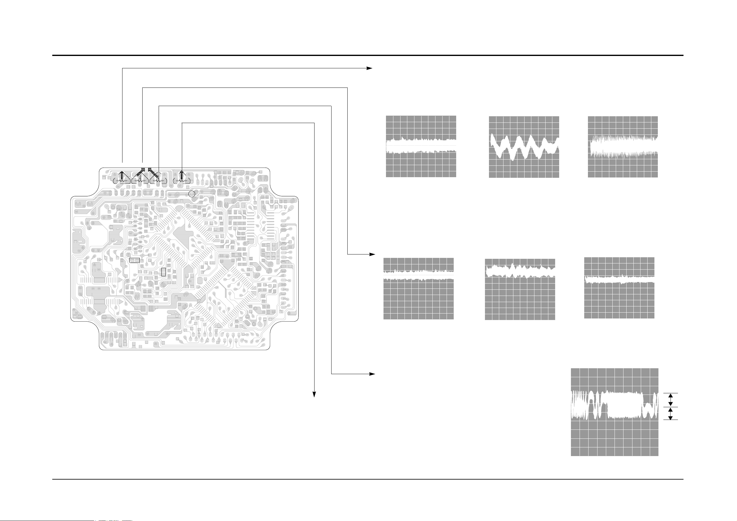
4-3 CD
TP2
TP1
Vref
NVR1704
NVR1703 NVR1702
NVR1701
TE CENTER
FE CENTER
E.F BAL
F.BIAS
0V
A
B
A=B
---100mV
---0V
---250mV
---0 V
---100mV
---0 V
---0 V
---0 V
---0 V
4-3-1 To Adjust FOCUS BIAS(STOP mode)
4-3-3 To Adjust Focus Gain (PLAY mode)
4-3-2 To Adjust Tracking Gain (PLAY mode)
4-3-4 To Adjust E/F Balance (PLAY mode)
1. Set Volt/Div of the oscilloscope to DC 100mV.
2. Ground the scope input and set the waveform to 0V, DC range.
3. Connect the GND terminal of the oscilloscope to
Vref, and (+) terminal to center of TP1.
4. Set NVR1701 to 0mV.
1. Connect the GND terminal of the oscilloscope to Vref and (+) terminal to TP2.
2. Load and play the disc
3. While the disc is running adjust the gain with NVR1704 as shown below.
1. Connect the GND terminal of the oscilloscope to Vref and (+) terminal to TP1.
2. Load and play the disc
3. While the disc is running adjust the gain with NVR1703 as shown in the following figure.
VOLT/DIV : 0.2V
TIME/DIV : 2mS
Normal frequency
Normal frequency
Low frequency
High frequency
Low frequency
High frequency
VOLT/DIV : 0.1V
TIME/DIV : 2mS
VOLT/DIV : 0.1V
TIME/DIV : 2mS
VOLT/DIV : 0.1V
TIME/DIV : 2mS
VOLT/DIV : 0.2V
TIME/DIV : 2mS
VOLT/DIV : 0.2V
TIME/DIV : 2mS
1. Set TIME/DIV of the oscilloscope to 2mS.
2. Set Volt/DIV of the oscilloscope to 0.5V.
3. Ground the scope input and set to DC
and then set the DC range.
4. Connect the GND terminal of the oscilloscope to Vref
and (+) terminal to center to TP2.
5. Load and play the disc.
6. Turn NVR1704 counterclockwise to the minimum value.
7. Raise NVR1702 and adjust the waveform so that its middle
comes to GND of the oscilloscope (or until the upper half
of waveform becomes symmetrical to the bottom half, A=B)
8. Adjust NVR1704 (arrow) for normal sound.
Alignment and Adjustments
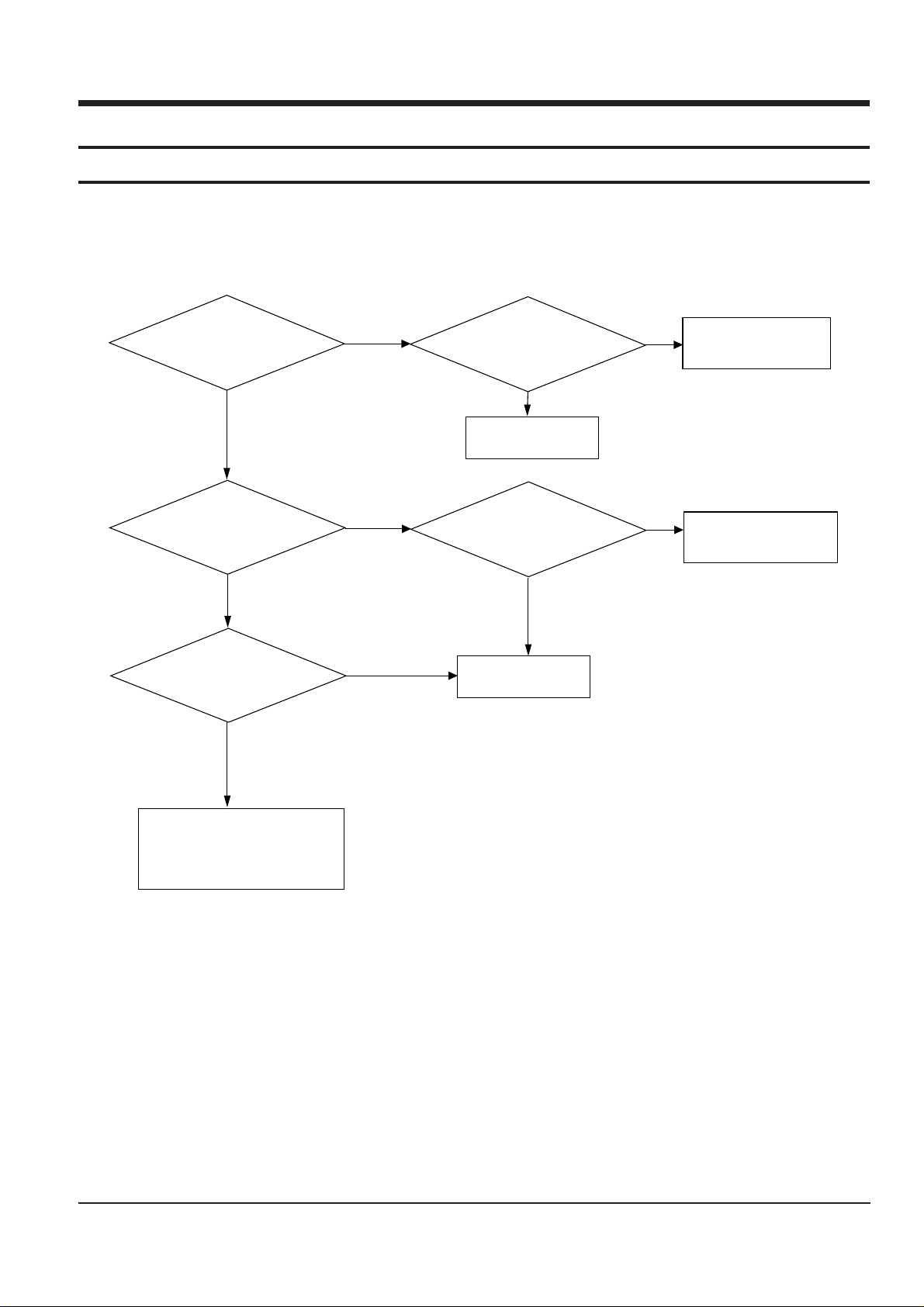
6. Troubleshooting
6-1 Main
6-1-1 Power Malfunction
Samsung Electronics 6-1
Front PCB µ-com VDD(5V)
normal?
UIC1 pin no. 9,36,37
Replace RIC1
Main PCB RIC1(BA3950) IN: 20V
Input voltage normal?
Yes
Check the Power PCB;
RF4 (T3.15 AL 250V)
Yes
Front PCB
Does UX1(4.5MHz)
oscillate ?
FRONT PCB POSNS
voltage normal ?
(pin no. 13 ;5.0V)
Check the Main PCB
RZD2,RC4,RR3,RR4,
RR2,RC1,RD1
Replace µ-com
Yes
Yes
Front PCB
When the power is
ON 'H' displays
at pin no. 49 ?(5V)
Yes
Connect Front PCB and Main PCB.
Check the connector Main PCB.
Wafer JWC3,JWC4
No
No
No
No
No
6-2 Samsung Electronics
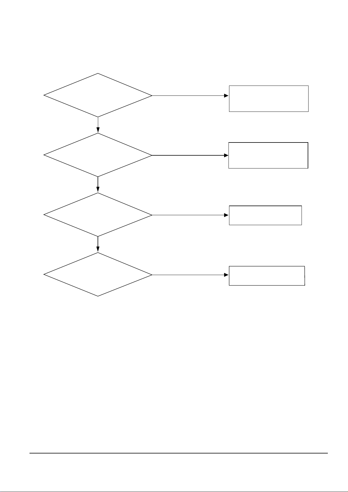
Troubleshooting
6-1-2 No Output
Yes
AQ1L/1R Base B+ ?
Yes
Is Mute selected ?
Headphone Jack short ?
Remove it with Remocon
Replace Headphone jack
soldering condition
Main PCB AIC1(LM1876TF)
pin no. 4,2,15
B+,B- circuits
Check the B+ power
source part in RD2(PBL403),
RC3 and RC14.
Yes
Confirm for TR short
replace it.
Yes
No
No
No
Samsung Electronics 6-3
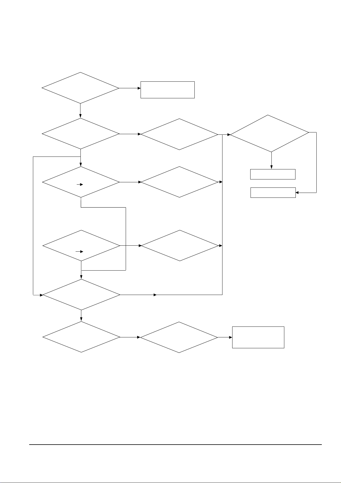
Troubleshooting
6-1-3 Tuner Malfunction (FM/AM)
IZD1 Voltage ok ?
Yes
Check TUNER IC(LA1836)
pin no.10 ; 7.6V
pin no.14 ; 6.5V
AM ; 0V ?
HZD1 (5.6V) Voltage ok?
HIC1 (LC72131) FM/AM BAND
Switching ok?
No
Yes
LC72131
CONTROL ok?
Yes
FM VT
LC72131 pin no.20
1.7V 7.5V ?
Yes
AM VT
LC72131 pin 20
Check the LC72131
CONTROL ok ?
Yes
Yes
Check HIC1
pin 20 ?
LPF(IL1, IL2)
output ok?
Check LC75394E function ok?
Check FEP interior
pattern, and any line
disconnections.
1) Power settion
defective ?
2) LC72131 Oscillator
(HX1 : 7.2MHz) ok ?
3) System line ok?
No
Yes
Check for µ-com IC
Replace LC72131
No
No
No
No
No
No
No
Yes
0.9V 7V
?
Check IZD1 (6.8V), IR6
 Loading...