

SAMSUNG MAX670RLC Service Manual
6+1 CD CHANGER MINI COMPONENT
1. Precautions
2. Product Specifications
3. Disassembly and Reassembly
4. Alignment and Adjustments
5. Special Circuit Descriptions
6. Troubleshooting
7. Exploded Views and Parts List
8. Electrical Parts List
9. Block Diagrams
10. PCB Diagrams
11. Wiring Diagram
12. Schematic Diagrams
CD SYNCHRO
DUBBING
HIGHNORMAL
RESET
DOLBY NRCOUNTER
DOLBY B NR
AUTO REVERSEAUTO REVERSE
REC/PLAY
2
PUSH EJECT
1
PLAYBACK
PUSH EJECT
AI OFF
1 2
REPEAT
REPEATPROGRAM
123456
EXTRA
OPEN/CLOSE
MIC
VOL.
MAXMIN
PHONES
POWER
ON/STAND BY
BIO VCR AUX ECHO
1-2-OFF
MIC
EQ SBS RELAX LEVEL
DSP SRS
MULTI JOG
VOLUME
MIN MAX
PASS POP ROCK JAZZ CLASSIC MUTE
BAND
TIMER/CLOCK MEMORY PRESET
SERVICE
Manual
6+1 CD CHANGER MINI
COMPONENT SYSTEM
MAX-670
CONTENTS
©
Samsung Electronics Co., Ltd. Oct. 1996. Code No. AH68-20108A
1. Precautions
Follow these safety, servicing and ESD precautions to prevent damage and protect against potential hazards
such as electrical shock and X-rays.
1-1 Safety Precautions
1. Be sure that all of the built-in protective
devices are replaced.
(Reading should
2. When reinstalling the chassis and its
assemblies, be sure to restore all protective
devices, including control knobs and
compartment covers.
3. Make sure that there are no cabinet
openings through which people-particularly children--might insert fingers
and contact dangerous voltages. Such
openings include the spacing between the
picture tube and the cabinet mask,
excessively wide cabinet ventilation slots,
and improperly fitted back covers.
Device
Under
Test
Test all
exposed metal
surfaces
2-Wire Cord
Also test with
plug reversed
(using AC adapter
plug as required)
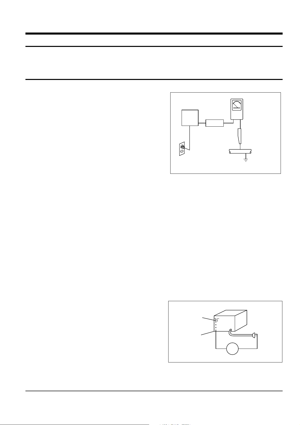
Fig. 1-1 AC Leakage Test
not be above
0.5mA)
Leakage
Currant
Tester
Earth
Ground
4. Design Alteration Warning:
Never alter or add to the mechanical or
electrical design of the unit. Example: Do
not add auxiliary audio or video connectors. Such alterations might create a safety
hazard. Also, any design changes or additions will void the manufacturer's warranty.
5. Leakage Current Hot Check (Figure 1-1):
Warning: Do not use an isolation
transformer during this test. Use a leakage-
current tester or a metering system that
complies with American National Standards
Institute (ANSI C101.1, Leakage Current for
Appliances), and Underwriters Laboratories
(UL Publication UL1410, 59.7).
With the unit completely reassembled, plug
the AC line cord directly into a 120V AC
outlet. With the unit's AC switch first in
the ON position and then OFF, measure the
current between a known earth ground
(metal water pipe, etc.) and all exposed
metal parts. Examples: Handle brackets,
metal cabinets, screwheads and control
shafts. The current measured should not
exceed 0.5 milliamp. Reverse the powerplug prongs in the AC outlet and repeat.
6. Insulation Resistance Cold Check:
(1) With the unit's AC plug disconnected
from the AC source, connect an electrical
jumper across the two AC prongs. (2) Set
the power switch to ON. (3) Measure the
resistance between the shorted AC plug and
any exposed metallic parts. Example:
Screwheads, antenna, control shafts or
handle brackets.
If any of the exposed metallic parts has a
return path to the chassis, the measured
resistance should be between 1 and 5.2
megohms. If there is no return path, the
measured resistance should be "infinite." If
the resistance is outside these limits, a shock
hazard might exist. See Figure 1-2
Antenna
Terminal
Exposed
Metal Part
ohm
Ohmmeter
Fig. 1-2 Insulation Resistance Test
Samsung Electronics 1-1

Precautions
1-1 Safety Precautions (Continued)
7. Components, parts and wiring that appear
to have overheated or that are otherwise
damaged should be replaced with parts
that meet the original specifications.
Always determine the cause of damage or
overheating, and correct any potential
hazards
8. Observe the original lead dress, especially
near the following areas: Antenna
wiring, sharp edges, and especially the
AC and high voltage power supplies.
Always inspect for pinched, out-of-place,
or frayed wiring. Do not change the
spacing between components and the
printed circuit board. Check the AC
power cord for damage. Make sure that
no wires or components touch thermally
hot parts.
1-2 Servicing Precautions
9. Product Safety Notice:
Some electrical and mechanical parts
have special safety-related characteristics
which might not be obvious from visual
inspection. These safety features and the
protection they give might be lost if the
replacement component differs from the
original--even if the replacement is rated
for higher voltage, wattage, etc.
10 Components that are critical for safety are
indicated in the circuit diagram by
shading, or . Use replacement
components that have the same ratings,
especially for flame resistance and
dielectric strength specifications. A
replacement part that does not have the
same safety characteristics as the original
might create shock, fire or other hazards.
Warning1: First read the "Safety Precautions" section of this manual. If some unforeseen circumstance creates a conflict
between the servicing and safety precautions, always follow the safety precautions.
1. Servicing precautions are printed on the
cabinet. Follow them.
2. Always unplug the unit's AC power cord
from the AC power source before
attempting to: (a) Remove or reinstall any
component or assembly, (b) Disconnect an
electrical plug or connector, (c) Connect a
test component in parallel with an
electrolytic capacitor.
3. Some components are raised above the
printed circuit board for safety. An
insulation tube or tape is sometimes used.
The internal wiring may be clamped to
prevent contact with thermally hot
components. Reinstall all such elements to
their original position.
4. After servicing, always check that the
screws, components and wiring have been
correctly reinstalled. Make sure that the
portion around the serviced part has not
been damaged.
5. Check the insulation between the blades of
the AC plug and accessible conductive parts
(examples: metal panels, input terminals
and earphone jacks).
6. Insulation Checking Procedure: Disconnect
the power cord from the AC source and
turn the power switch ON. Connect an
insulation resistance meter (500V) to the
blades of the AC plug.
The insulation resistance between each
blade of the AC plug and accessible
conductive parts (see above) should be
greater than 1 megohm.
7. Never defeat any of the B+ voltage
interlocks. Do not apply AC power to the
unit (or any of its assemblies) unless all
solid-state heat sinks are correctly installed.
8. Always connect a test instrument's ground
lead to the instrument chassis ground
before connecting the positive lead; always
remove the instrument's ground lead last.
Samsung Electronics1-2
1-3 Precautions for Electrostatically Sensitive Devices (ESDs)
Precautions
1. Some semiconductor ("solid state") devices
are easily damaged by static electricity.
Such components are called Electrostatically
Sensitive Devices (ESDs). Examples include
integrated circuits and some field-effect
transistors. The following techniques will
reduce the occurrence of component
damage caused by static electricity.
2. Immediately before handling any
semiconductor components or assemblies,
drain the electrostatic charge from your
body by touching a known earth ground.
Alternatively, wear a discharging
wrist-strap device. (Be sure to remove it
prior to applying power--this is an electric
shock precaution.)
3. After removing an ESD-equipped assembly,
place it on a conductive surface such as
aluminum foil to prevent accumulation of
electrostatic charge.
4. Do not use freon-propelled chemicals.
These can generate electrical charges that
damage ESDs.
5. Use only a grounded-tip soldering iron
when soldering or unsoldering ESDs.
6. Use only an anti-static solder removal
device. Many solder removal devices are
not rated as "anti-static" (these can
accumulate sufficient electrical charge to
damage ESDs).
7. Do not remove a replacement ESD from its
protective package until you are ready to
install it. Most replacement ESDs are
packaged with leads that are electrically
shorted together by conductive foam,
aluminum foil or other conductive
materials.
8. Immediately before removing the protective
material from the leads of a replacement
ESD, touch the protective material to the
chassis or circuit assembly into which the
device will be installed.
9. Minimize body motions when handing
unpackaged replacement ESDs. Motions
such as brushing clothes together, or lifting
a foot from a carpeted floor can generate
enough static electricity to damage an ESD.
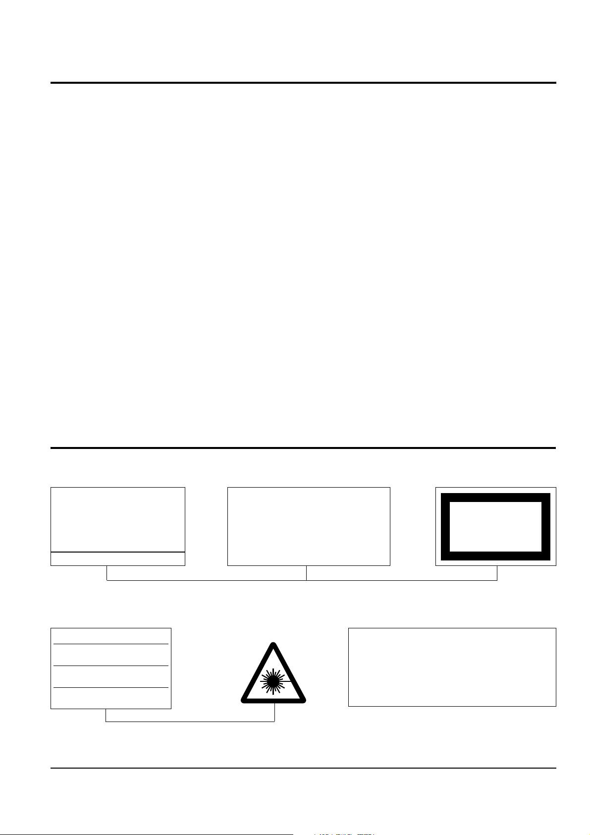
1-4 Special Precautions and Warning Labels for Laser Products
(UL)
This Product Complies with
DHHS Rules 21CFR, Sub
chapter J.At date of Manufacture
(SCAN)
CAUTION : INVISIBLE LASER RADIATION WHEN OPEN
AND INTERLOCKS DEFEATEO AVOIDEXPOSURE TO BEAM
ADVARSEL:USYNLIG LASERSTRÅLING VED ABNING
NÅR SIKKERHEDSAFBRYDERE ER UDE AF FUNKTION
UNDGA UDSAETTELSE FOR STRALING
VARO:AVATTAESSA JA SUOJALUKITUS OHITETTAESSA
OLET ALTTINA NAKYMATTÖMALLE LASERSATEILYLLE ALA
KATSO SATEESEEN!
VARNING:OSYNLIG LASERSTRÅLNING NAR DENNA DEL
AR OPPNAD OCH SPARREN AR URKOPPLAD BETRAKTA
EJSTRÅLEN!
CERTIFIED ONLY TO CANADIAN
ELECTRICAL CODE.
CERTIFIE EN VERTU DU CODE
CANADIAN DE LELETRICITE
SEULEMENT
Fig. 1-3 Warning Labels (Location: Enclosure Block)
(EU)
(CSA)
UL : Manufactured for U.S.A. Market.
CSA : Manufactured for Canadian Market.
EU : Manufactured for European Market.
SCAN : Manufactured for Scandinavian
Market.
(EU)
CLASS 1
LASER PRODUCT
Fig. 1-4 Warning Labels (Location: Disc Clamper, Inner Side of Unit Door or Nearby Unit Chassis )
Samsung Electronics 1-3
Precautions
1-4 Special Precautions and Warning Labels for Laser Products (Continued)
1-4-1 Warnings
1. When servicing, do not approach the LASER
exit with the eye too closely. In case it is
necessary to confirm LASER beam emission,
be sure to observe from a distance of more
than 30 cm from the surface of the objective
lens on the optical pick-up block.
2. Do not attempt to handle the objective lens
when the DISC is not on the tray.
1-4-2 Laser Diode Specifications
Material: GaAs+ GaAlAs
Wavelength: 760-800 nm
Emission Duration: Continuous
Laser Output: 0.2 mw (measured at a
1.6 mm distance from the objective lens
surface on the optical pick-up block.)
1-4-3 Handling the Optical Pick-up
1. Static electricity from clothing or the body
may cause electrostatic breakdown of the
laser diode in the Optical Pickup. Follow
this procedure:
2. Place a conductive sheet on the work bench
(i.e., the black sheet used for wrapping
repair parts.) Note: The surface of the work
bench should be covered by a copper
ground plane, which is grounded.
3. The repair technician must wear a wrist
strap which is grounded to the copper sheet.
4. To remove the Optical Pickup block:
Place the set on the conductive sheet, and
momentarily touch the conductive sheet
with both hands. (While working, do not
allow any electrostatic sources--such as
clothes--to touch the unit.)
5. Ground the "Short Terminal" (located on the
PCB, inside the Pickup Assembly) before
replacing the Pickup. This terminal should
be shorted whenever the Pickup Assembly
is lifted or moved.
short
terminal
SOH91VI(LDP)
short terminal
SOH91CI(CAR,walkman)
6. After replacing the Pickup, reopen the Short
Terminal. See diagrams below:
1M
THE UNIT
(1) WRIST-STRAP
FOR GROUNDING
short
terminal
SOH-A1
(CMS-V10,CMS-V30)
1M
SOH94T4N
(CMS-V10,CMS-V30)
CONDUCTIVE SHEET
short
terminal
Samsung Electronics1-4

2. Specifications
Power source
Power consumption
Dimmensions(mm)
220V
280W
270(W)x317(H)x333(D)
Power output
Total harmonic distortion
Frequency range
Signal to noise ratio
Channel separation
Input sensitivity
Frequency range
Usable sensitivity
Signal to noise ratio
If rejection ratio
Total harmonic distortion
Separation(Stereo)
Frequency range
Usable sensitivity
Signal to noise ratio
If rejection ratio
Total harmonic distortion
Frequency range
Usable sensitivity
Signal to noise ratio
Frequency range
WOW FLUTTER
Erasing effect
Signal to noise ratio
Total harmonic distortion
Frequency response
Signal to noise ratio
Channel separation
Total harmonic distortion
87.5 ~ 108MHz
1µV
62dB
60dB
0.45%
35dB
522 ~ 1611KHz
600µV
40dB
30dB
2%
146 ~ 290KHz
1000µV
35dB
125Hz ~ 12.5KHz
0.15%
60dB
40dB
2.5%
20Hz ~ 20KHz(¡ 1dB)
100dB(1kHz 0dB)
80dB(1kHz 0dB)
0.01%(1kHz 0dB)
90W/CH(6Ω)
10%
20Hz ~ 20kHz
75 dB
50 dB (1 KHz)
AUX 400mV
General
Amp
Tuner
Cassette Deck
Compact Disc
FM
AM
LW
(Option)
Samsung Electronics 2-1
* Specifications are subject to change without notice.
3. Disassembly and Reassembly
* Before removing the unit, be sure to unplug.
3-1 Amp and Tuner Section
3-1-1 Cabinet-Top
1. Remove 9 screws ! holding the Cabinet-Top.
2. Remove the Cabinet-Top in the direction of arrow.
FRONT
BOTTOM
REAR
TOP
1
Figure 3-1
Samsung Electronics 3-1
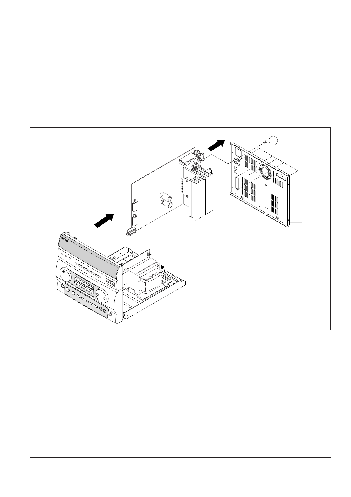
3-1-2 Cabinet-Rear
1. Remove 7 screws ! holding the Cabinet-Rear.
2. Remove the Cabinet-Rear in the direction of arrow.
3. Remove the Main PCB in the direction of arrow.
Figure 3-2
3-2 Samsung Electronics
REAR
1
MAIN PCB
Disassembly and Reassembly
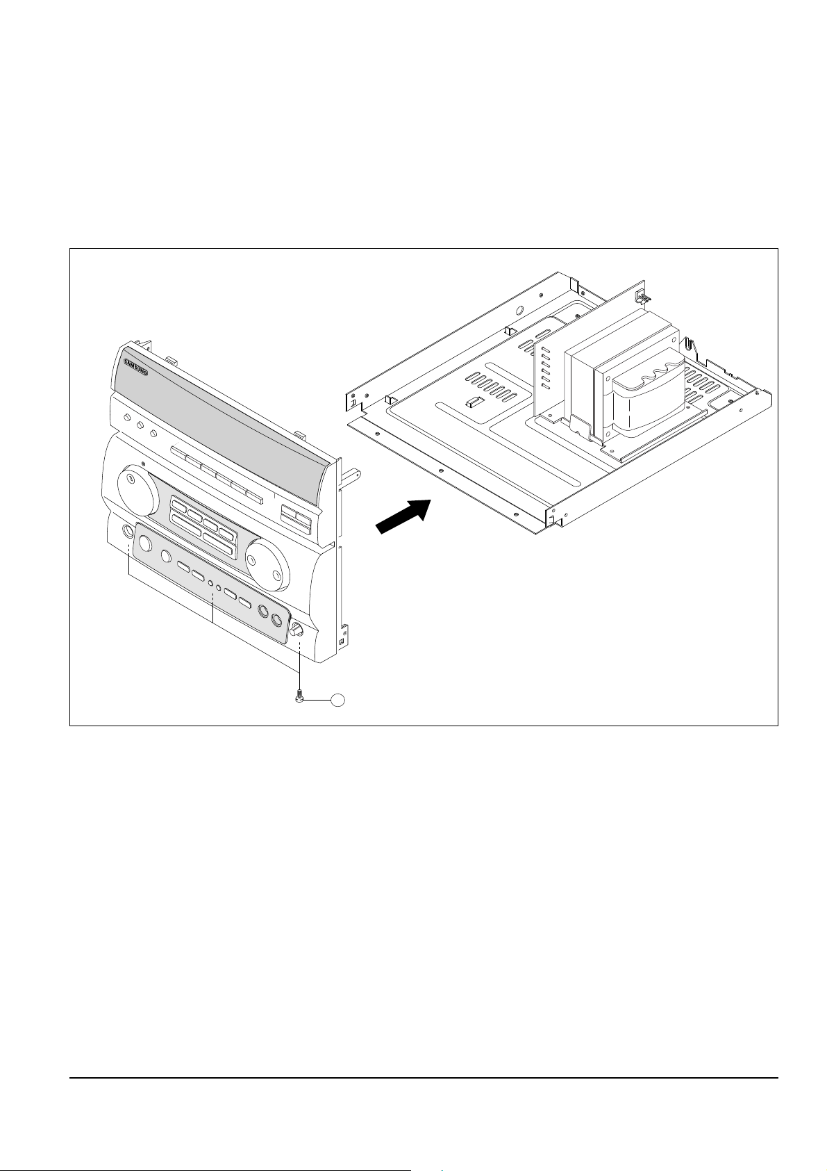
3-1-3 Cabinet-Front
1. Remove 3 screws ! holding the Cabinet-Front.
2. Remove the Cabinet-Front from the Bottom.
1
Figure 3-3
Samsung Electronics 3-3
Disassembly and Reassembly
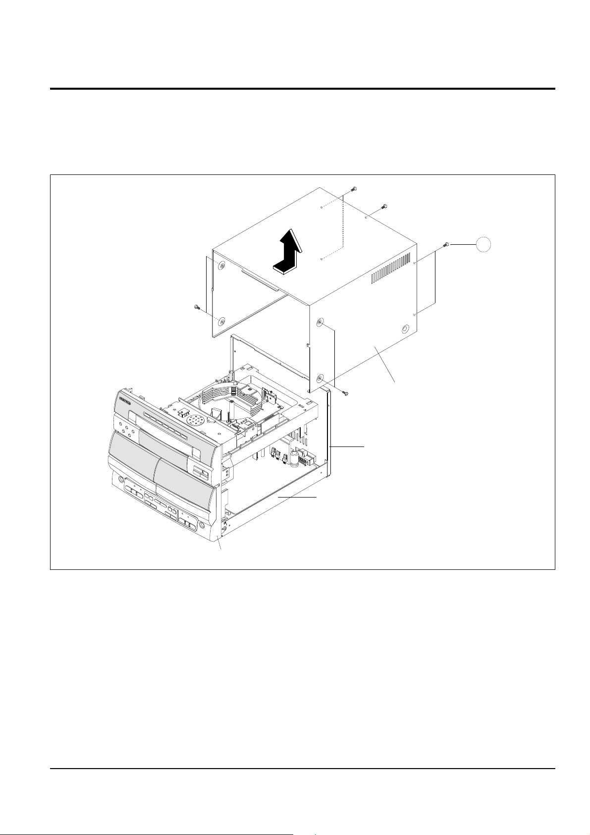
Figure 3-4
3-4 Samsung Electronics
3-2 Cassette Deck and CD Section
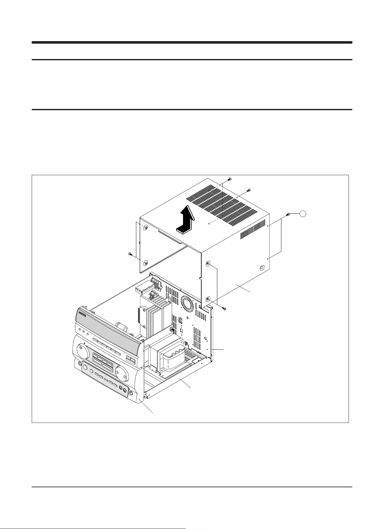
3-2-1 Cabinet-Top
1. Remove 9 screws ! holding the Cabinet-Top.
2. Remove the Cabinet-Top in the direction of arrow.
1
FRONT
BOTTOM
REAR
TOP
Disassembly and Reassembly
4-1Samsung Electronics
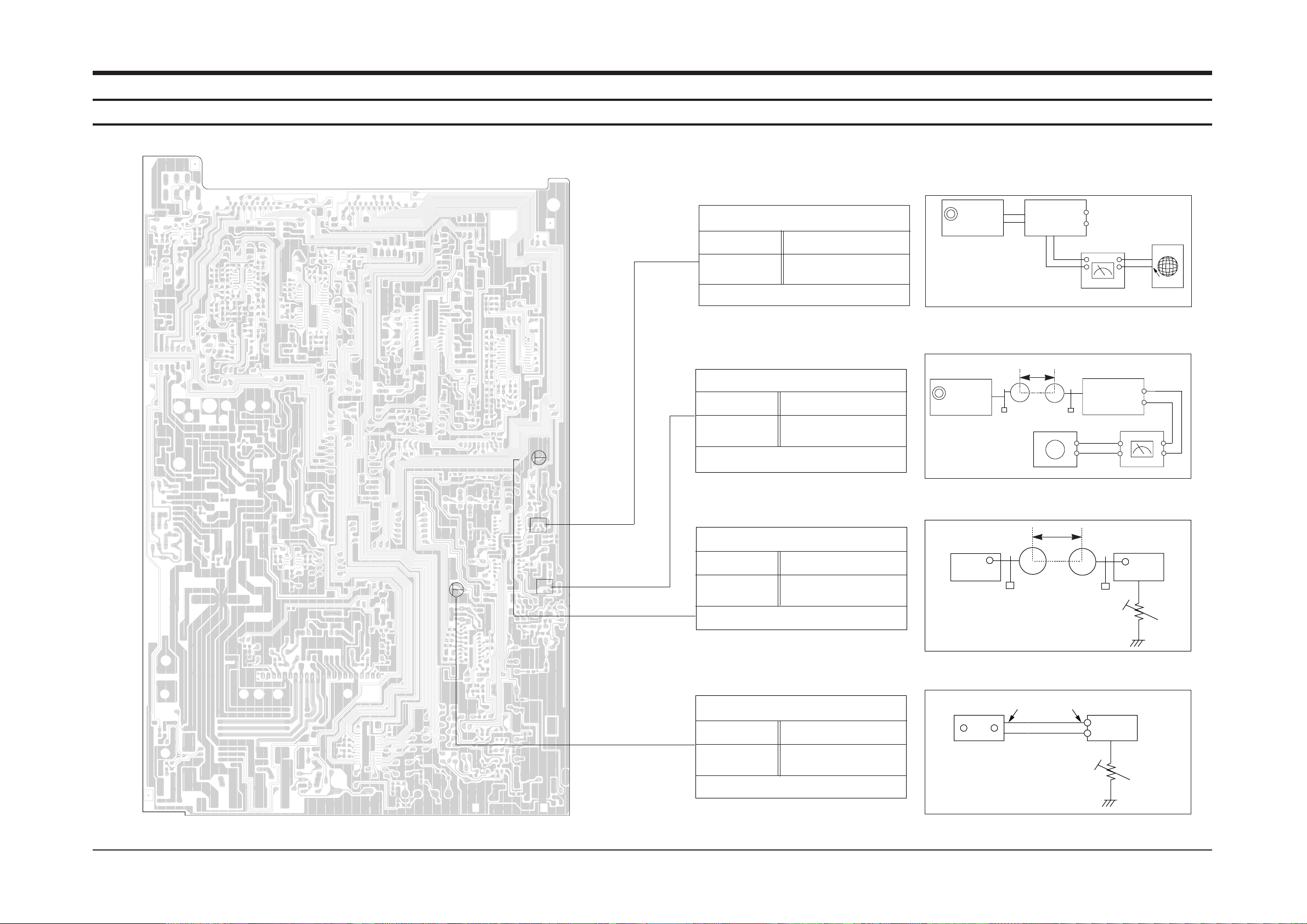
4. Alignment and Adjustments
4-1 Tuner Section
FM T.H.D Adjustment
SSG FREQ.
Adjustment
point (TL2)
Minimum output(Figure4-1)
Level : Maximum (Figure4-2)
SSG FREQ.
Adjustment
point (TL1)
SSG FREQ.
Adjustment
point (TL1)
“TUNED” is shown of FLT (Figure4-3)
Adjustment
point (TL1)
SSG FREQ.
“TUNED” is shown of FLT (Figure4-4)
FM
antenna
Terminal
Speaker
Terminal
Input
Input
Figure 4-1 IF CENTER and T.H.D Adjustment
Output
Voltmeter
Oscilloscope
FM S.S.G
SET
Output
GND
TVR2
TL2
TL1
TVR1
AM IF Adjustment
Figure 4-3 AM Search Level Adjustment
Figure 4-4 FM Search Level Adjustment
FM S.S.G
GND
Oscilloscope
VTVM
60 cm
30dB
FM IN
FM Antenna
SET
5 kB
AM Search Level Adjustment
Figure 4-2 AM IF Level Adjustment
AM S.S.G
AM
Antenna
Terminal
FM Search Level Adjustment
* Note : Be sure to adjust the AM for Tuner Search Level.
(If AM is adjusted, FM is adjusted automatically.)
* Note : Adjust FM S.S.G Level to
EMF 21dB (Included Loss)
60 cm
AM S.S.G
20KB
SET
98MHz
FM DETECTIR COIL
594KHz
AM IF COIL
999KHz
SEMI-VR (20KB)
98MHz
SEMI-VR (5KB)
3KHZ 1%
5700~6300KHz
Samsung Electronics4-2
Alignment and Adjustments
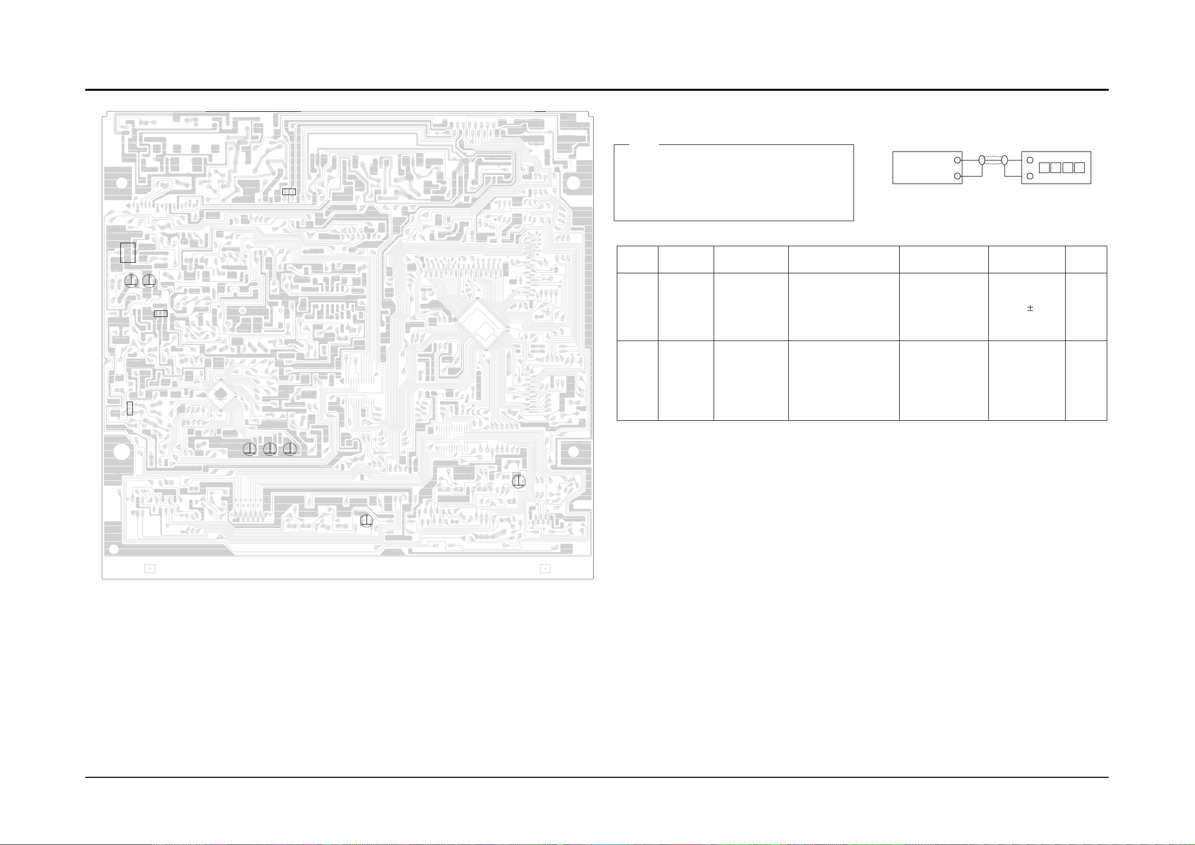
4-2 Cassette Deck Section
1) Measuring Tape i) MTT-111(or equivalent)
(Tapes recorded with 3kHz )
ii) MTT-5512(or equivalent)
2) Connect the Cassette Deck to the
frequency counter as in Figure 4-5
Note
4-2-1 To Adjust Tape Speed
Figure 4-5
Cassette Deck
Frequency Counter
Line Out
TP1
Output
LSR1R
LSR1L
JSR3R
JSR2R
JSR1R
CSR1
TP3
CSR2
LL2
TP1
TP2
NOR
SPEED
Control
counter
HI SPEED
Control
OUT
(connected
tothe
frequency
counter)
Same as
above
1) A-Deck: MTT-111
2) Press PLAY SW
button
3) B-Deck: Same as
below
1) A-Deck: MTT-111
2) B-Deck: MTT-5512
3) Press Hi Speed
dubbing switch
Turn CSR1,2 to
left and right.
Fixed
Check
1
2
Step
To Adjust
Item
Standard
Remark
Pre-Setup
Condition
Pre-Setup
VTVM
400mV 5%
105KHz 5%
VTVM
(7V 5%)
Max output
and same
phase both
channels.
300mV 0.5dB
Max output
and same
phase (both
channels).
300mV 0.5dB
4-3Samsung Electronics
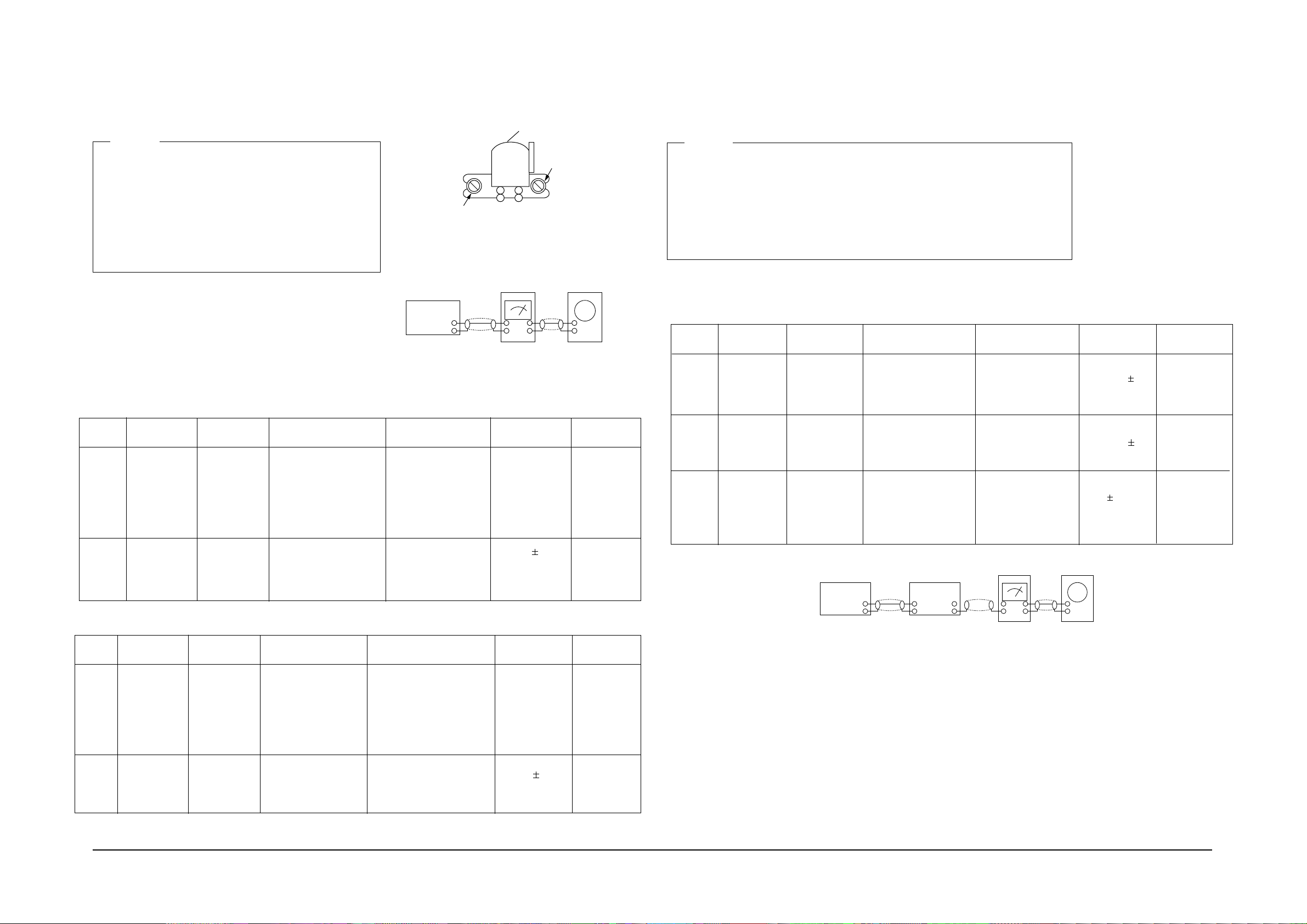
Figure 4-6
Figure 4-7
Cassette Deck
LINE OUT
TP1
V H
Oscilloscope
Recording/Play head
REVERSE
PLAY
Input Output
Azimuth Control Knob
Alignment and Adjustments
1) Before the actual adjustment, clean the
replay/recording head.
2) Measuring tape :
i) MTT-114NA (or equivalent 12.5 kHz AZIMUTH
control).
ii) MTT-150 (or equivalent : Dolby level 200mwb/m)
3) Dolby NR SW OFF
4) The cassette deck is connections as shown in figure4-6.
NOTES
4-2-2 To Adjust Replay Head
Step
Step
To Adjust
To Adjust
Item
Item
Standard
Standard
Remark
Remark
Pre-Setup
Condition
Pre-Setup
Condition
Pre-Setup
Pre-Setup
AZIMUTH
PlayBack
out Level
TP1 OUT
(VTVM is
connected
to the
scope)
Same as
above
After putting MTT
-114NA into Deck 1.
1) Press FWD
PLAY button.
2) Press REV
PLAY button.
PLAY MTT-150
on Deck1.
1) Turn the control
knob to as shown
in Figure 4-6.
2) Adjust the right
control screw to
playback Rev.
Mode.
L-CH : Turn JSR1R
to the right and
left
R-CH : Fixed
After
adjustment
secure it
with
REGION
LOCK.
See the
diagram
for
adjustment
locations
After
adjustment
secure it
with
REGION
LOCK.
See the
diagram
for
adjustment
locations
1
2
AZIMUTH
PlayBack
out Level
TP3 OUT
(VTVM is
connected
to the scope)
Same as
above
After putting
MTT-114NA into
Deck 2.
1) Press FWD
PLAY button.
2) Press REV
PLAY button.
PLAY MTT-150
on Deck2.
1) Turn the control knob
to left and right as shown
in the Figure 4-6.
2) Adjust the right
control screw to
playback Rev. Mode.
L-CH :Turn JSR2R to
the right and left;
R-CH : Fixed
1
2
1) Adjust 1-Deck Replay Level
2) Adjust 2-Deck Replay Level
1) Connect the measuring instruments as shown in Figure 4-8
2) Set the DOLBY NR Switch off.
3) Measuring tape :
MTT-5512 ( or equivalent : normal recording )
4) The input signals supply 400Hz 400mV into AUX IN of AMP (AUDIO OSC).
NOTES
Step
Item
Pre-Setup
Condition
Normal
electric
current for
recording
BIAS OSC.
FREQUENCY
BIAS electric
current
Connect to TP2
as in Figure 4-8
and read
VTVM
Connect the
frequency
counter to
TP1
Connect to
TP1 as in
Figure 4-8
and read the
VTVM
Insert MTT-5512
into Deck 2,
then press
REC button.
Insert MTT-5512
into Deck 2,
then press
REC button.
Insert MTT-5512
into Deck 2,
then press
REC button.
L-CH : DSR2L to
the right and left.
R-CH : Fixed
Turn BIAS oscillator frequency coil
(LL2) to the right
and left.
L-CH : DSR1L and
R-CH: DSR1R to
the right and left.
See diagram
for adjustment
locations.
See diagram
for adjustment
locations.
See diagram
for adjustment
locations.
1
2
3
4-2-3 To Adjust PlayBack
Figure 4-8
In Out
VTVM
AUDIO OSC
Oscilloscope
Cassette Deck
AUX IN
TP1
Pre-Setup
To Adjust
Standard
Remark
Samsung Electronics4-4
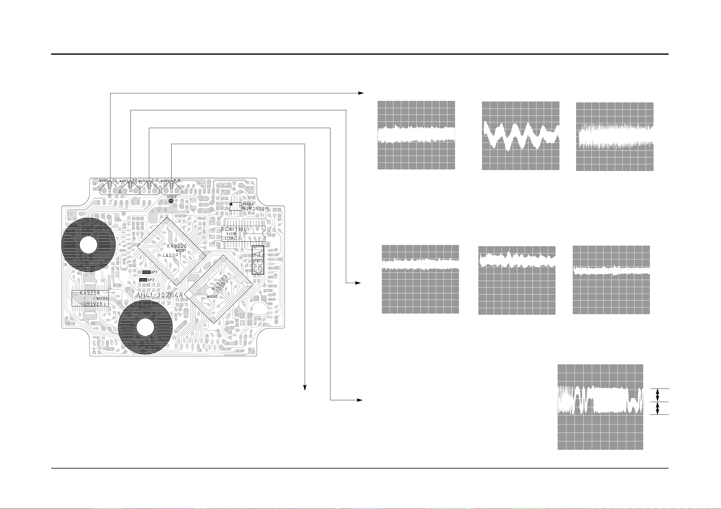
4-3 CD Section
0V
A
B
A=B
---100mV
---0V
---250mV
---0 V
---100mV
---0 V
---0 V
---0 V
---0 V
4-3-1 To Adjust FOCUS BIAS(STOP mode)
1. Set Volt/Div of the oscilloscope to DC 100mV.
2. Ground the scope input and set the waveform to 0V, DC range.
3. Connect the GND terminal of the oscilloscope to
Vref, and (+) terminal to center of TP1.
4. Set WVR4 to 0mV.
4-3-4 To Adjust E/F Balance (PLAY mode)
1. Set TIME/DIV of the oscilloscope to 2mS.
2. Set Volt/DIV of the oscilloscope to 0.5V.
3. Ground the scope input and set to DC
and then set the DC range.
4. Connect the GND terminal of the oscilloscope to Vref
and (+) terminal to center to AP2.
5. Load and play the disc.
6. Turn WVR1 counterclockwise to the minimum value.
7. Raise WVR3 and adjust the waveform so that its middle
comes to GND of the oscilloscope (or until the upper half
of waveform becomes symmetrical to the bottom half, A=B)
8. Adjust WVR1 (arrow) for normal sound.
VOLT/DIV : 0.1V
TIME/DIV : 2mS
VOLT/DIV : 0.1V
TIME/DIV : 2mS
VOLT/DIV : 0.1V
TIME/DIV : 2mS
Normal Frequency
Low Frequency High Fequency
4-3-3 To Adjust Focus Gain (PLAY mode)
1. Connect the GND terminal of the oscilloscope to Vref and (+) terminal to TP1.
2. Load and play the disc
3. While the disc is running adjust the gain with NVR1703 as shown in the following figure.
4-3-2 To Adjust Tracking Gain (PLAY mode)
1. Connect the GND terminal of the oscilloscope to Vref and (+) terminal to AP2.
2. Load and play the disc
3. While the disc is running adjust the gain with WVR1 as shown below.
Normal Frequency
VOLT/DIV : 0.2V
TIME/DIV : 2mS
Low Frequency
VOLT/DIV : 0.2V
TIME/DIV : 2mS
VOLT/DIV : 0.2V
TIME/DIV : 2mS
High Frequency
Alignment and Adjustments
Samsung Electronics 5-1
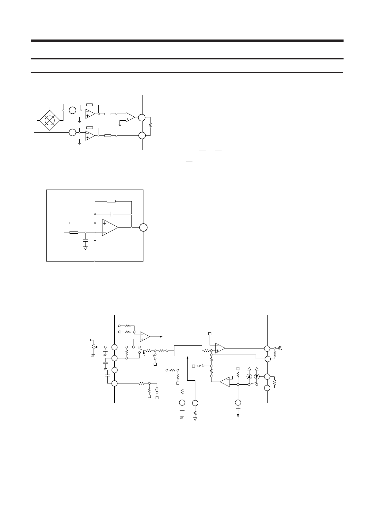
RF I-V Amp(1) and RF I-V Amp(2) are converted to voltage via
internal resistance of 58k½ from the current of PD1(A+C) and PD2(B+D):
This voltage is added to RF summing amplifier.
The signal (A+B+C+D) is applied to RFO (No. 66 terminal).
RF output voltage is calculated as follows :
VFE = (R2/R1) x (V2-V1) = 5.4(V2-V1)
This FOCUS ERROR voltage is sent to FOCUS SERVO .
VRF = -R3 x (iPD1 + iPD2)
VRF = -R3 x (V1/R1 + V2/R2)
VRF = -R3 x ( + )
VRF = - x (V1 + V2)
10K 10K
V 1 V 2
10K
R3
66
Photo Detector
B
CA
D
PD1
PD2
58K
RF I-V AMP(1)
58K
10K
R2
RF I-V AMP(2)
V2
R1
10K
RF SUMMING
V1 AMP
RFO
RF
66
R3
65
74
73
5-1-1 RF Amp (KA9220) : WIC01
5-1-2 FOCUS ERROR Amp(KA9220) : WIC01
59
R2
174K
C1 25P
FE
FOCUS
ERROR
AMP
164K
32K
C2 25P
-(A+C)
-(B+D)
R1
V1 32K
5-1-3 FOCUS SERVO SYSTEM (KA9220) : WIC01
When FS3 is ON, high frequency gain decreases (time constant set by pin17, pin19, and capacitor connected
to internal resistance).
The capacitor between pin 18 and GND sets the time constant to pass the low frequency operated in PLAY mode.
The maximum frequency of focus phase compensation is inversely proportional to the resistance connected to
pin 7. Focus search peak is about 1.1 Vp-p, and is inversely proportional to the resistance connected to pins 22,23
(if this resistance changes, the peak of track jump and sled kick change).
The inversion input of FZC comparator is set to 5.7% of the difference between Vcc and VC(pin69) {{5.7% x (Vcc-Vc)}.
Note : If the resistance connected to pin7 changes, the phase compensation peak of focus, tracking, sled servo changes.
At the same time, 'op-amp' dynamic range and offset voltage also change.
3.6K
20
21
47
48
60K
FZC
0.0022
20K
0.1UF
0.1UF
FDFCT
HFGD
EFR
FE2
470K
DFCT
FS4
20K 48K
58
60
62
46K
580K FS3
FSW
470K
130K
0.1UF
27
40K
6
PFSET
FS2
PHASE
COMPENSATION
92K
40K
10K
3
4.7UF
FSCH
FS1
50K
5.5U 11U
VREG
180K
ISET
FCE
120K
FOCUS
COIL
FSEO
FE1
61
5-1 CD
FOCUS ERROR Amp is the circuit which amplifies the difference
between RF I-V Amp(1) output (A+C) and RF I-V Amp(2)
output(B+D).
These two signals are supplied to (-) and (+) input terminals of
FOCUS ERROR Amp. The FOCUS ERROR signal resulting from this
difference voltage is applied to FE (Terminal No.57).
The FE output voltage of this low frequency component varies
according to {(A+C) - (B+D)}.
VFE is calculated as follows :
5. Special Circuit Descriptions
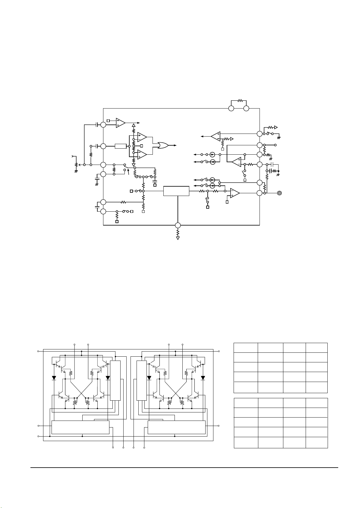
5-1-5 Motor Drive(LB1649) : UIC4
22 23
40
41
39
47
48
7
15
16
54
52
50
51
0.022UF
TZC
0.047UF
150K
BPF
1K
1K
TZC
100K
ATC
20K
TE 1
TE2
470K
100K
ATS
TDFC1
0.1UF
680K
66PF
10K
DFCT
0.1UF
RTG
20K
TGSW
470K
TG2
82K
110K
PHASE
COMPENSATION
S STOP
1K
100K
S STOP
SLED
SLEI
SLEN
10K
56K
100K
ISET VREG
180K
SLED
DRIVER
120K
100K
TKEO
TKEI
TM2
TM6
TM5
TM4
5.5U
TM3
5.5U
10K
90K
TM7
PFSET
470K
8
TRACKING
COIL
5-2
Special Circuit Descriptions
Samsung Electronics
10
3
OUT1
OUT2
VCC1
1
IN 1
Fin
11
2
IN 2
12
6
VZ1
VZ2
IN3
5
IN4
8
7
VCC2
9
4
OUT3
OUT4
Input Logic Input Logic
Pre-Driver
Pre-Driver
IN 1 2 OUT1 OUT2
0 0 L L
1 0 H L
0 1 L H
1 1 L L
IN 3 IN 4 OUT3 OUT4
0 0 L L
1 0 H L
0 1 L H
1 1 L L
5-1-4 Tracking Sled Servo System (KA9220) : WIC01
The capactor between pin 15 and 16 attenuates the high frequency when TG2 is off. The maximum frequency of
tracking phase compensation is inversely proportional to the resistance connected to pin 7 (about 1.2kHz at 470k).
The tracking jump (FWD and REV) is decided when TM3 and TM4 are ON, and the peak voltage induced from
tracing coil is decided by the both TM3 and TM4 current values and feed back resistance of pin 47.
Track jump max voltage = TM3 (TM4) current x feedback resistance.
FWD or REV sled kick occnrs when TM5 or TM6 is ON, and the peak voltage added to sled motor is decided by
TM5 or TM6 current and the feedback resistance of pin 41.
Sled jump max. voltage = TM5(TM6) current x feedback resistance
Each SW current is decided by the resistance connected to pin 22 and 23.
When the resistance is about 150½,
TM3 or TM4 = 11µA,
TM5 or TM6 = 22µA,
This current is inversely proportional to the resistor, variable within a range of t 5 to 40 µA for TM3.
STOP is the ON/OFF detection signal for the limit SW (or the sled motor's innermost cirumference).
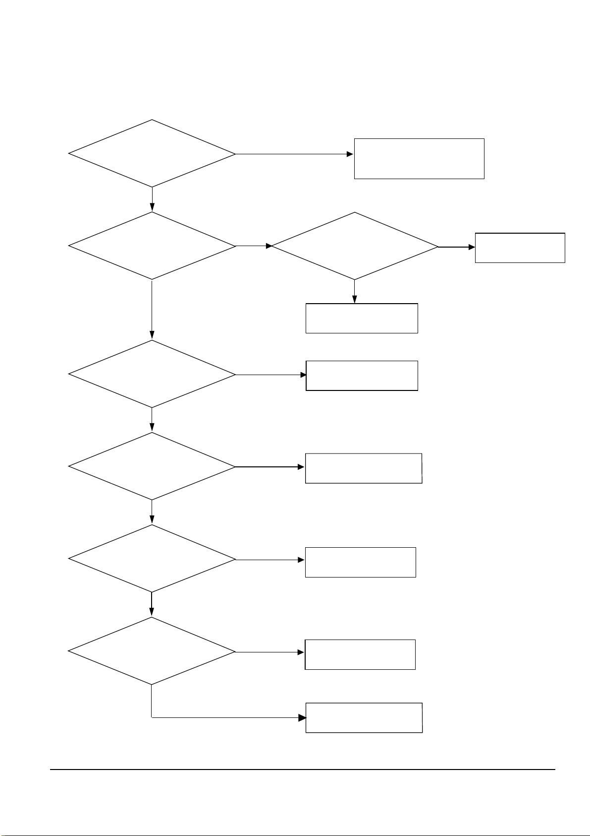
Samsung Electronics 6-1
6-1 The Amp Section
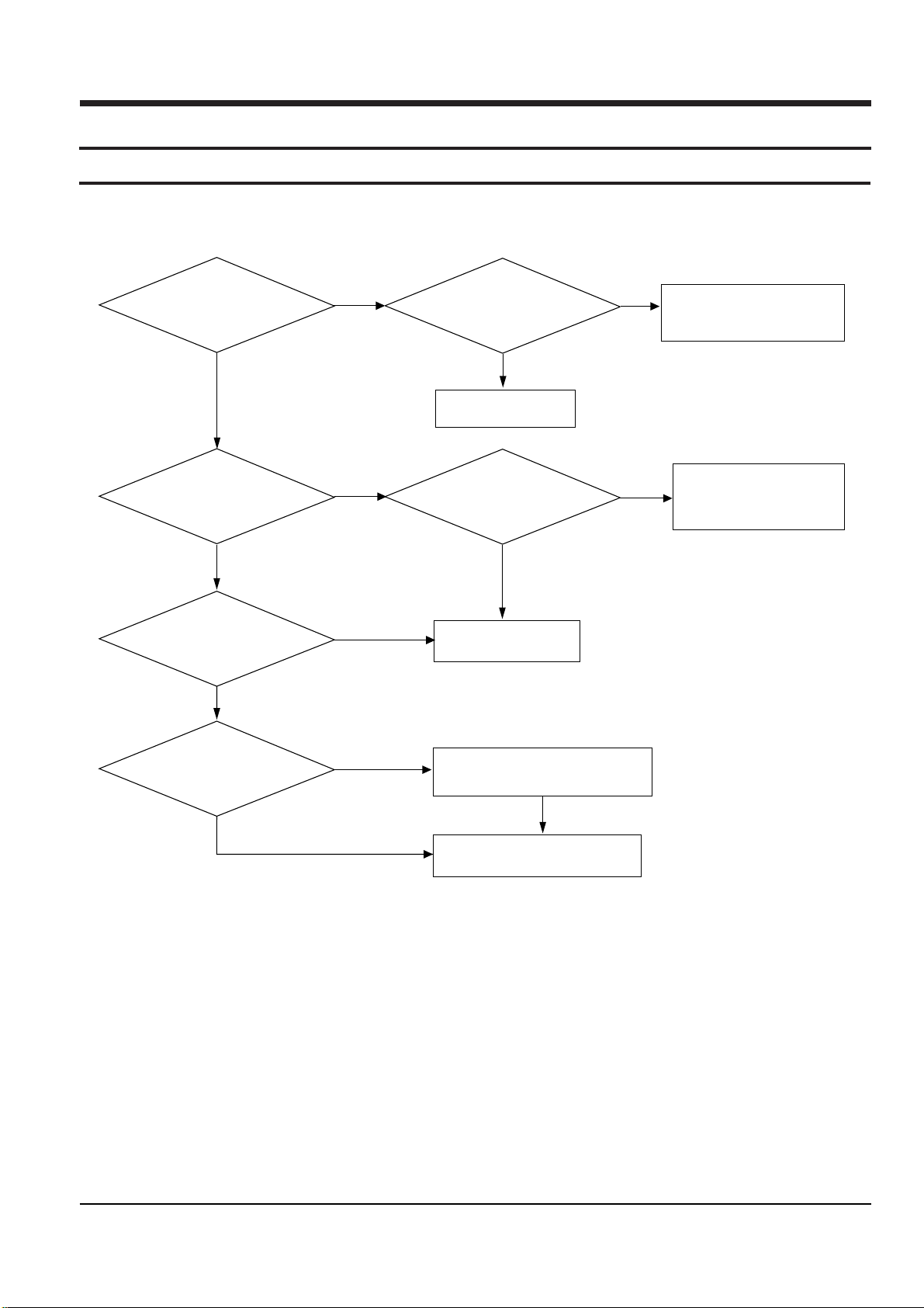
6-1-1 Power Malfunction
6. Troubleshooting
Main PCB µ-com VDD(5V)
normal?
UIC1 pin no. 18,47,90
O
Front PCB
X
Main PCB POSNS
voltage normal ?
(pin no. 28 ; 4.5V)
X
Check the Front PCB ; UQ1
Check the Main PCB ;
RD3,RZD4,PC11,PR33
PR9,PR10,PC12
Check the Power PCB ;
PIC2,PR4,3
X
RF3,4(T2A 250V)
Main PCB UIC5(78L05) IN : 8V
Input voltage normal ?
O
X
Replace UIC5
Does UX2(12MHz)
oscillate ?
O
O
At the base of
Main PCB ; PQ3
Base High Display ?
Replace µ-com
X
X
O
Front PCB,
When the power is
ON 'H', displays
at pin no.84 ? (5V)
Connect Front PCB and Main PCB &
Check the connector Main PCB
Wafer CCW2,CMW2
O
Replace µ-com
O
O
Connector inserted
correctly?
X
O
Check voltage : AC 5V
at FRONT-PCB FLT?
X
Check Main-PCB & Front PCB
connection and the voltage of
CCW2, pins19,20 (AC 5V)
O
Check voltage at UIC1
pin no. 48(-36V)
X
Check the voltage of PZD2 (-36V)
Reinsert the connector.
Replace UIC1
6-2 Samsung Electronics
Troubleshooting
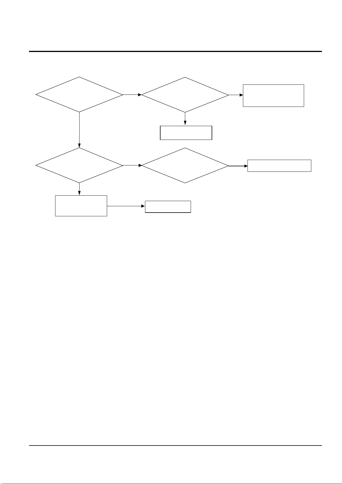
6-1-2 F.L.T Malfunction
AQ OC2,OC8 pin no.7 ;
Main PCB OC2,OC8
(STK4221), pin no.11,13
; B+,B circuits
Check the B+ power
source part in PBD2(GBU6D),
PC1 and PC2.
O
O
O
Is Mute selected ?
Confirm for TR short
Replace it
Remove it with Remocon
O
X
Check if the output line is
short
X
X
X
B- (-0.3V)
Check the mute
circuit OQ1(KSR2003)
base B+ (0V)
X
Replace OD8
Replace OQ1
O
OQ4,OQ2
Base B+ ?
O
Headphone jack
Short ?
Replace Headphone jack
X
soldering condition
O
Front PCB
µ-com pin no.5 ;
Check the "H"
Replace µ-com
X
Samsung Electronics 6-3
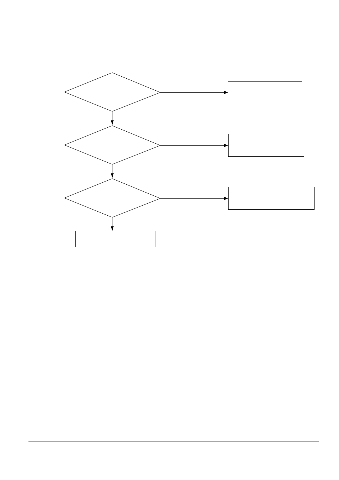
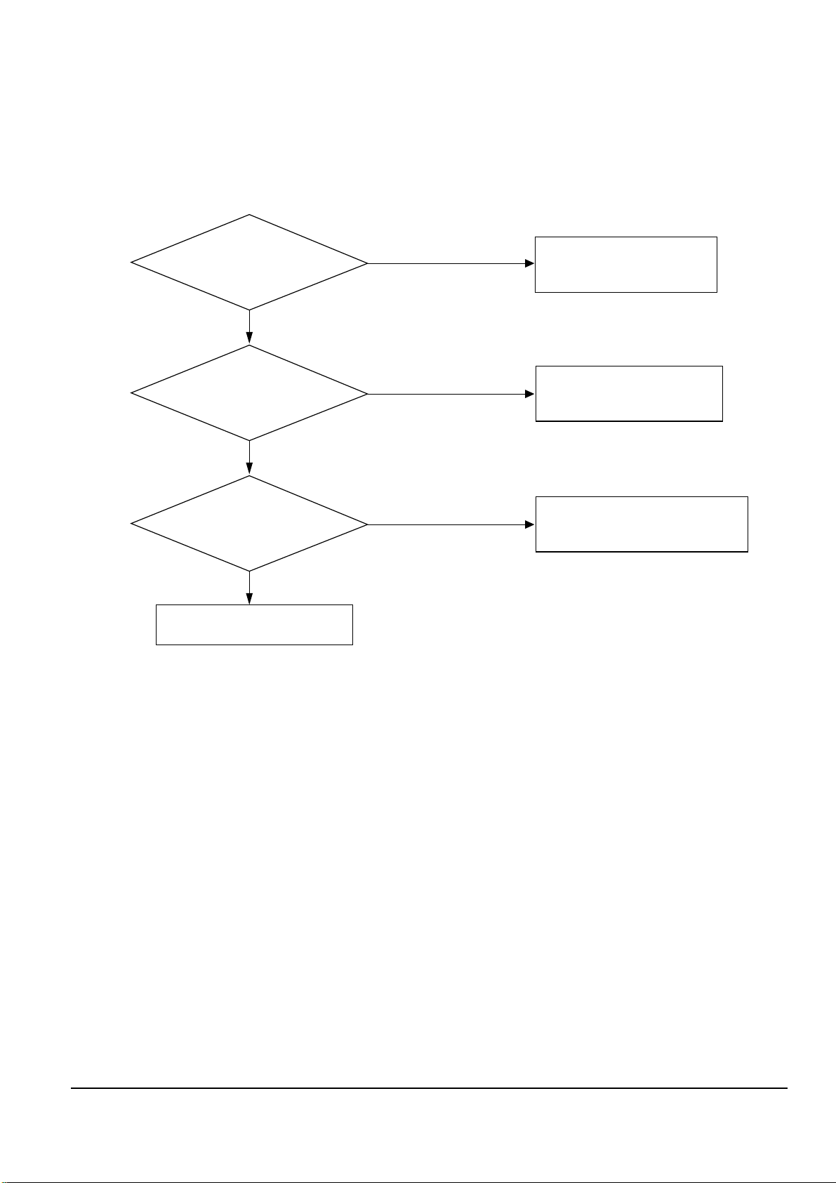
Troubleshooting
6-1-3 No Output
Main PCB µ-com VDD(5V)
normal?
UIC1 pin no. 18,47,90
O
Main PCB
X
Main PCB POSNS
voltage normal ?
(pin no. 29 ; 4.5V)
X
Check the Main PCB ; CSW1
X
Main PCB RIC4(BA7805) IN : 5V
Input voltage normal ?
O
X
Replace RIC4
Does UX2(12MHz)
oscillope ?
O
Main PCB
Check µ-com vpp
pin no.48
Check the Power PCB ;
RD1,RD2(IN5392)
At the base of Main PCB ;
RFS1,2 (T2A 250V)
X
Replace UIC1
6-4 Samsung Electronics
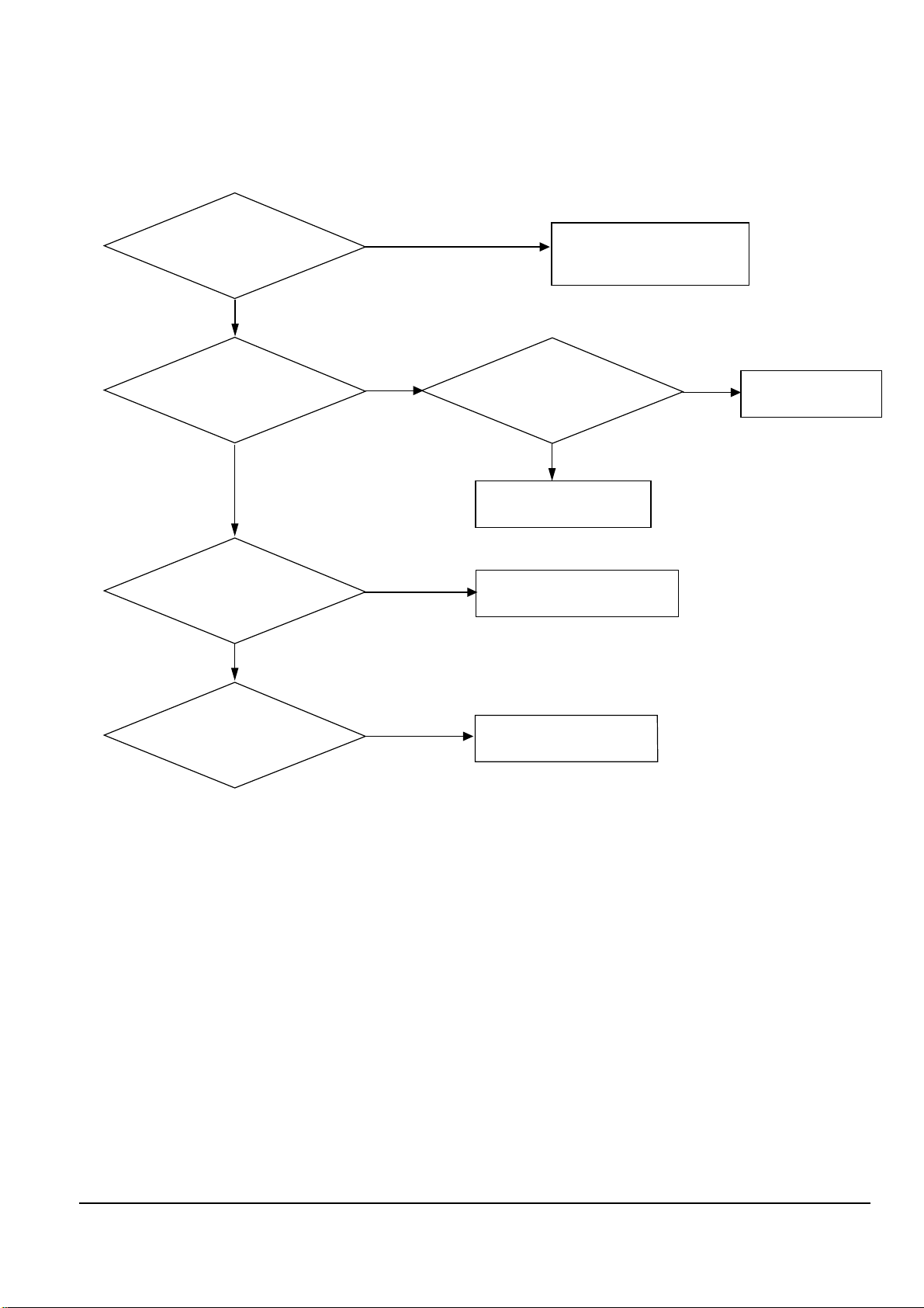
6-2 The Deck Section
6-2-1 Power Malfunction
Troubleshooting
O
Connector inserted
correctly?
X
O
Check voltage : AC 5V
at FRONT-PCB FLT?
X
Check Main-PCB & Front PCB
connection and the voltage of
CCW2, pins1,2 (AC 5V)
O
Check voltage at UIC1
pin no. 48(-36V)
X
Check the voltage at pin no.8
of CSW1
Reinsert the connector.
Replace UIC1
Samsung Electronics 6-5
6-2-2 F.L.T Malfunction
Troubleshooting
Main PCB DIC2
(HC14066), pin no. 7,14
; Check signal
Check the B+ power
source part in RIC3(KA7812),
IN ; 15V, OUT ;12V
O
O
O
Check signal of pin no. 43,45
of JIC1 ?
Replace JIC1
X
X
X
X
Check B+ of pin no. 10
of DIC1 ?
X
Check RIC3(KA7812)
IN ; 15V, OUT ; 12V
Replace RQ4
O
Check signal of pin no. 1,2
of JIC1 ?
Check signal of pin no.
3,13V of DIC1 ?
Check B+ ; 10V of pin no.22
of JIC1 ?
6-6 Samsung Electronics
6-2-3 No Output
Troubleshooting
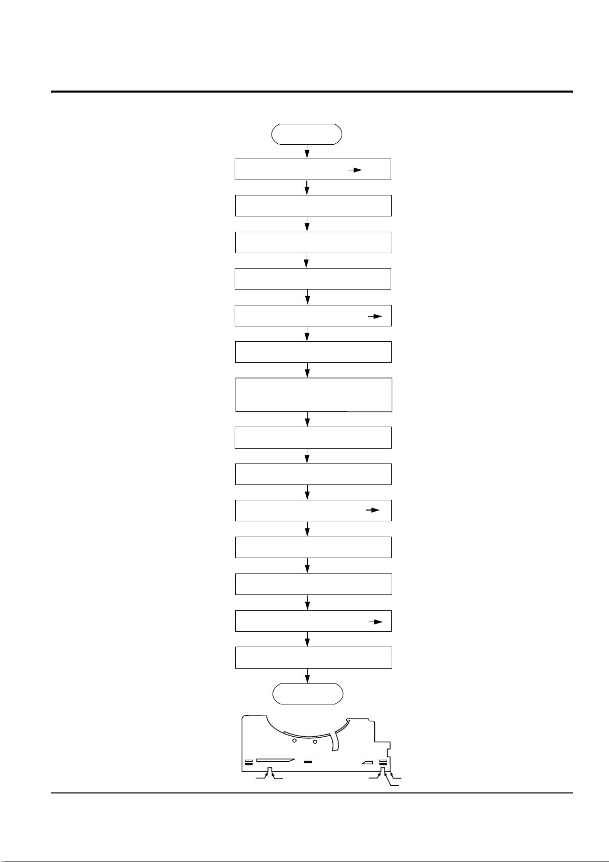
PICK-UP LIMIT SW (ON OFF)
PICK-UP UNIT SW (DOWN)
DISC CASE P.SENSOR(L)
LOAD
LOADING PLATE P.SENSOR(H L)
LOADING MOTOR STOP
LOADING MOTOR (CCW)
30mS (BRAKE)
LOADING MOTOR STOP 40mS
LOADING MOTOR (CCW)
LOADING PLATE P.SENSOR(L H)
LOADING MOTOR STOP 30mS
LOADING MOTOR (CW)
LOADING PLATE P.SENSOR(H L)
LOADING MOTOR STOP
END
C
C
C
a
b
c
e
d
LOADING MOTOR(CW)
Samsung Electronics
6-7
Troubleshooting
6-3 CD Section
6-3-1 Load Operation
 Loading...