

Page 1
3 CD CHANGER MINI COMPONENT
1. Precautions
2. Product Specifications
3. Disassembly and Reassembly
4. Alignment and Adjustments
5. Special Circuit Descriptions
6. Troubleshooting
7. Exploded Views and Parts List
8. Electrical Parts List
9. Block Diagrams
10. PCB Diagrams
11. Wiring Diagram
12. Schematic Diagrams
SERVICE
Manual
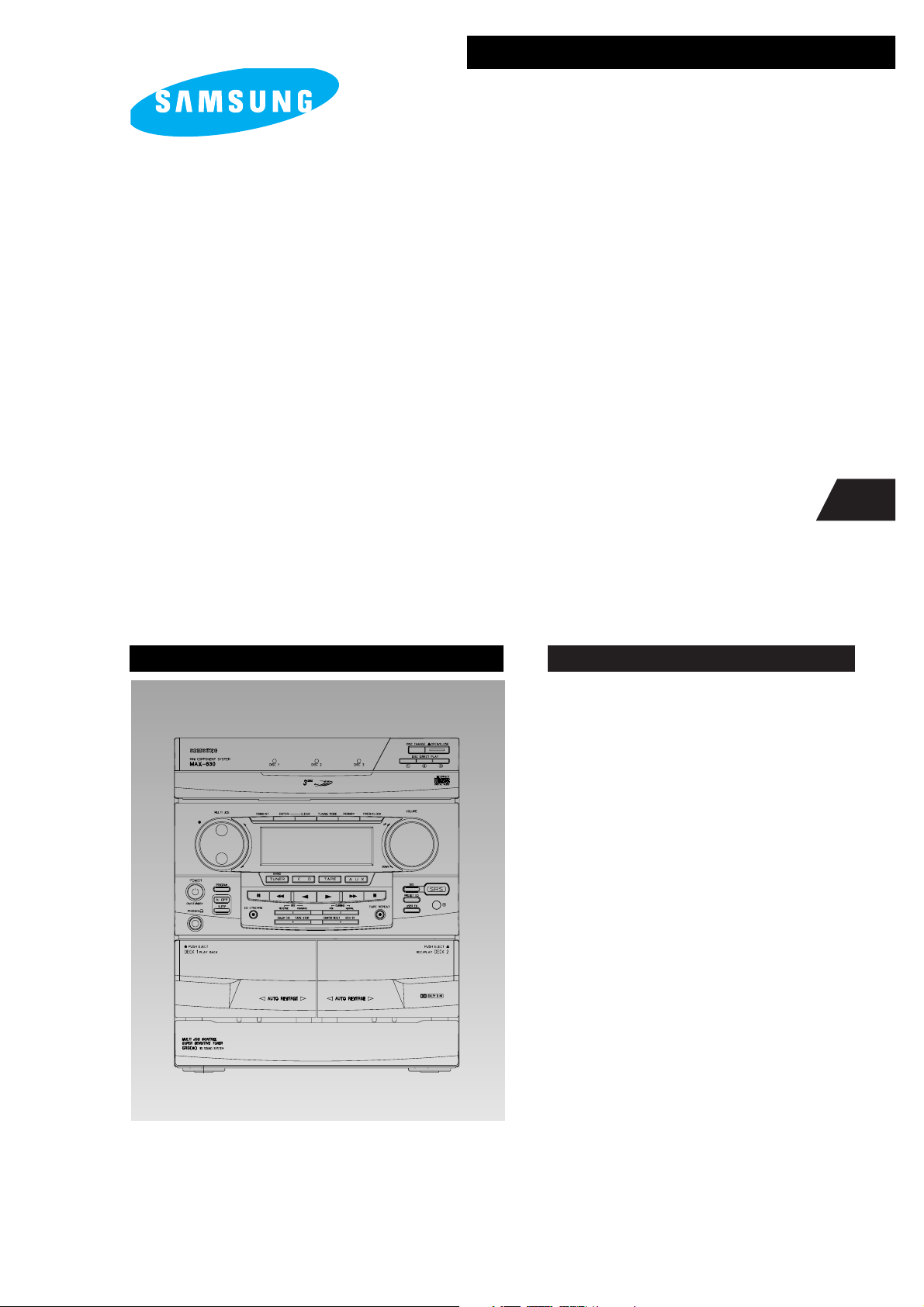
3 CD CHANGER MINI
COMPONENT SYSTEM
MAX-630
CONTENTS
©
Samsung Electronics Co., Ltd. June. 1996. Code No. AH68-20106A
Page 2
1. Precautions
Follow these safety, servicing and ESD precautions to prevent damage and protect against potential hazards
such as electrical shock and X-rays.
1-1 Safety Precautions
1. Be sure that all of the built-in protective
devices are replaced.
(Reading should
2. When reinstalling the chassis and its
assemblies, be sure to restore all protective
devices, including control knobs and
compartment covers.
3. Make sure that there are no cabinet
openings through which people-particularly children--might insert fingers
and contact dangerous voltages. Such
openings include the spacing between the
picture tube and the cabinet mask,
excessively wide cabinet ventilation slots,
and improperly fitted back covers.
Device
Under
Test
Test all
exposed metal
surfaces
2-Wire Cord
Also test with
plug reversed
(using AC adapter
plug as required)
Fig. 1-1 AC Leakage Test
not be above
0.5mA)
Leakage
Currant
Tester
Earth
Ground
4. Design Alteration Warning:
Never alter or add to the mechanical or
electrical design of the unit. Example: Do
not add auxiliary audio or video connectors. Such alterations might create a safety
hazard. Also, any design changes or additions will void the manufacturer's warranty.
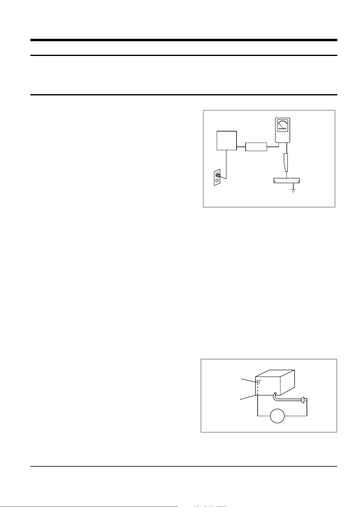
5. Leakage Current Hot Check (Figure 1-1):
Warning: Do not use an isolation
transformer during this test. Use a leakagecurrent tester or a metering system that
complies with American National Standards
Institute (ANSI C101.1, Leakage Current for
Appliances), and Underwriters Laboratories
(UL Publication UL1410, 59.7).
With the unit completely reassembled, plug
the AC line cord directly into a 120V AC
outlet. With the unit's AC switch first in
the ON position and then OFF, measure the
current between a known earth ground
(metal water pipe, etc.) and all exposed
metal parts. Examples: Handle brackets,
metal cabinets, screwheads and control
shafts. The current measured should not
exceed 0.5 milliamp. Reverse the powerplug prongs in the AC outlet and repeat.
6. Insulation Resistance Cold Check:
(1) With the unit's AC plug disconnected
from the AC source, connect an electrical
jumper across the two AC prongs. (2) Set
the power switch to ON. (3) Measure the
resistance between the shorted AC plug and
any exposed metallic parts. Example:
Screwheads, antenna, control shafts or
handle brackets.
If any of the exposed metallic parts has a
return path to the chassis, the measured
resistance should be between 1 and 5.2
megohms. If there is no return path, the
measured resistance should be "infinite." If
the resistance is outside these limits, a shock
hazard might exist. See Figure 1-2
Antenna
Terminal
Exposed
Metal Part
ohm
Ohmmeter
Fig. 1-2 Insulation Resistance Test
Samsung Electronics 1-1
Page 3

Precautions
1-1 Safety Precautions (Continued)
7. Components, parts and wiring that appear
to have overheated or that are otherwise
damaged should be replaced with parts
that meet the original specifications.
Always determine the cause of damage or
overheating, and correct any potential
hazards
8. Observe the original lead dress, especially
near the following areas: Antenna
wiring, sharp edges, and especially the
AC and high voltage power supplies.
Always inspect for pinched, out-of-place,
or frayed wiring. Do not change the
spacing between components and the
printed circuit board. Check the AC
power cord for damage. Make sure that
no wires or components touch thermally
hot parts.
1-2 Servicing Precautions
9. Product Safety Notice:
Some electrical and mechanical parts
have special safety-related characteristics
which might not be obvious from visual
inspection. These safety features and the
protection they give might be lost if the
replacement component differs from the
original--even if the replacement is rated
for higher voltage, wattage, etc.
10 Components that are critical for safety are
indicated in the circuit diagram by
shading, or . Use replacement
components that have the same ratings,
especially for flame resistance and
dielectric strength specifications. A
replacement part that does not have the
same safety characteristics as the original
might create shock, fire or other hazards.
Warning1: First read the "Safety Precautions" section of this manual. If some unforeseen circumstance creates a conflict
between the servicing and safety precautions, always follow the safety precautions.
1. Servicing precautions are printed on the
cabinet. Follow them.
2. Always unplug the unit's AC power cord
from the AC power source before
attempting to: (a) Remove or reinstall any
component or assembly, (b) Disconnect an
electrical plug or connector, (c) Connect a
test component in parallel with an
electrolytic capacitor.
3. Some components are raised above the
printed circuit board for safety. An
insulation tube or tape is sometimes used.
The internal wiring may be clamped to
prevent contact with thermally hot
components. Reinstall all such elements to
their original position.
4. After servicing, always check that the
screws, components and wiring have been
correctly reinstalled. Make sure that the
portion around the serviced part has not
been damaged.
5. Check the insulation between the blades of
the AC plug and accessible conductive parts
(examples: metal panels, input terminals
and earphone jacks).
6. Insulation Checking Procedure: Disconnect
the power cord from the AC source and
turn the power switch ON. Connect an
insulation resistance meter (500V) to the
blades of the AC plug.
The insulation resistance between each
blade of the AC plug and accessible
conductive parts (see above) should be
greater than 1 megohm.
7. Never defeat any of the B+ voltage
interlocks. Do not apply AC power to the
unit (or any of its assemblies) unless all
solid-state heat sinks are correctly installed.
8. Always connect a test instrument's ground
lead to the instrument chassis ground
before connecting the positive lead; always
remove the instrument's ground lead last.
Samsung Electronics1-2
Page 4
1-3 Precautions for Electrostatically Sensitive Devices (ESDs)
Precautions
1. Some semiconductor ("solid state") devices
are easily damaged by static electricity.
Such components are called Electrostatically
Sensitive Devices (ESDs). Examples include
integrated circuits and some field-effect
transistors. The following techniques will
reduce the occurrence of component
damage caused by static electricity.
2. Immediately before handling any
semiconductor components or assemblies,
drain the electrostatic charge from your
body by touching a known earth ground.
Alternatively, wear a discharging
wrist-strap device. (Be sure to remove it
prior to applying power--this is an electric
shock precaution.)
3. After removing an ESD-equipped assembly,
place it on a conductive surface such as
aluminum foil to prevent accumulation of
electrostatic charge.
4. Do not use freon-propelled chemicals.
These can generate electrical charges that
damage ESDs.
5. Use only a grounded-tip soldering iron
when soldering or unsoldering ESDs.
6. Use only an anti-static solder removal
device. Many solder removal devices are
not rated as "anti-static" (these can
accumulate sufficient electrical charge to
damage ESDs).
7. Do not remove a replacement ESD from its
protective package until you are ready to
install it. Most replacement ESDs are
packaged with leads that are electrically
shorted together by conductive foam,
aluminum foil or other conductive
materials.
8. Immediately before removing the protective
material from the leads of a replacement
ESD, touch the protective material to the
chassis or circuit assembly into which the
device will be installed.
9. Minimize body motions when handing
unpackaged replacement ESDs. Motions
such as brushing clothes together, or lifting
a foot from a carpeted floor can generate
enough static electricity to damage an ESD.
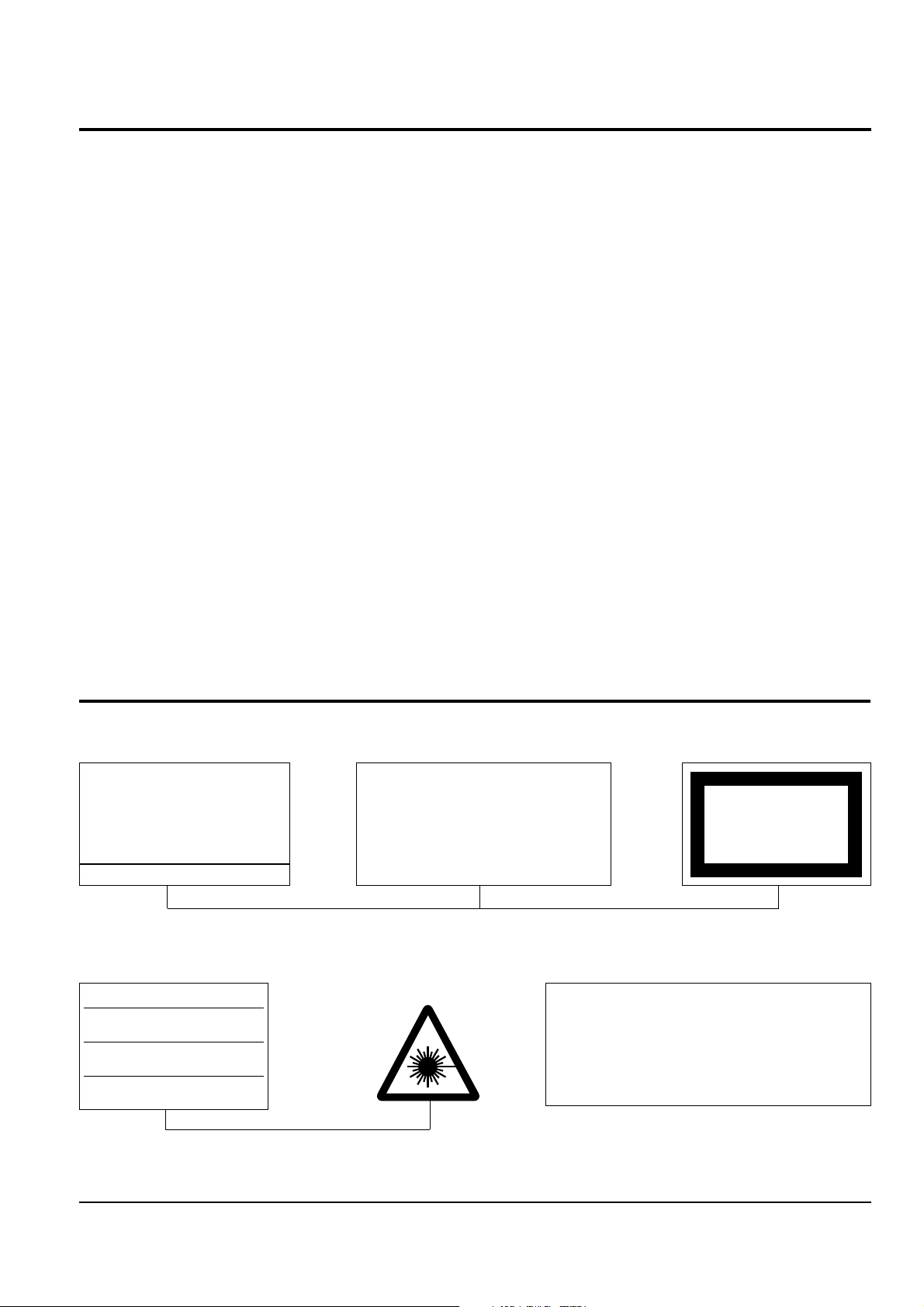
1-4 Special Precautions and Warning Labels for Laser Products
(UL)
This Product Complies with
DHHS Rules 21CFR, Sub
chapter J.At date of Manufacture
(SCAN)
CAUTION : INVISIBLE LASER RADIATION WHEN OPEN
AND INTERLOCKS DEFEATEO AVOIDEXPOSURE TO BEAM
ADVARSEL:USYNLIG LASERSTRÅLING VED ABNING
NÅR SIKKERHEDSAFBRYDERE ER UDE AF FUNKTION
UNDGA UDSAETTELSE FOR STRALING
VARO:AVATTAESSA JA SUOJALUKITUS OHITETTAESSA
OLET ALTTINA NAKYMATTÖMALLE LASERSATEILYLLE ALA
KATSO SATEESEEN!
VARNING:OSYNLIG LASERSTRÅLNING NAR DENNA DEL
AR OPPNAD OCH SPARREN AR URKOPPLAD BETRAKTA
EJSTRÅLEN!
CERTIFIED ONLY TO CANADIAN
ELECTRICAL CODE.
CERTIFIE EN VERTU DU CODE
CANADIAN DE LELETRICITE
SEULEMENT
Fig. 1-3 Warning Labels (Location: Enclosure Block)
(EU)
(CSA)
UL : Manufactured for U.S.A. Market.
CSA : Manufactured for Canadian Market.
EU : Manufactured for European Market.
SCAN : Manufactured for Scandinavian
Market.
(EU)
CLASS 1
LASER PRODUCT
Fig. 1-4 Warning Labels (Location: Disc Clamper, Inner Side of Unit Door or Nearby Unit Chassis )
Samsung Electronics 1-3
Page 5
Precautions
1-4 Special Precautions and Warning Labels for Laser Products (Continued)
1-4-1 Warnings
1. When servicing, do not approach the LASER
exit with the eye too closely. In case it is
necessary to confirm LASER beam emission,
be sure to observe from a distance of more
than 30 cm from the surface of the objective
lens on the optical pick-up block.
2. Do not attempt to handle the objective lens
when the DISC is not on the tray.
1-4-2 Laser Diode Specifications
Material: GaAs+ GaAlAs
Wavelength: 760-800 nm
Emission Duration: Continuous
Laser Output: 0.2 mw (measured at a
1.6 mm distance from the objective lens
surface on the optical pick-up block.)
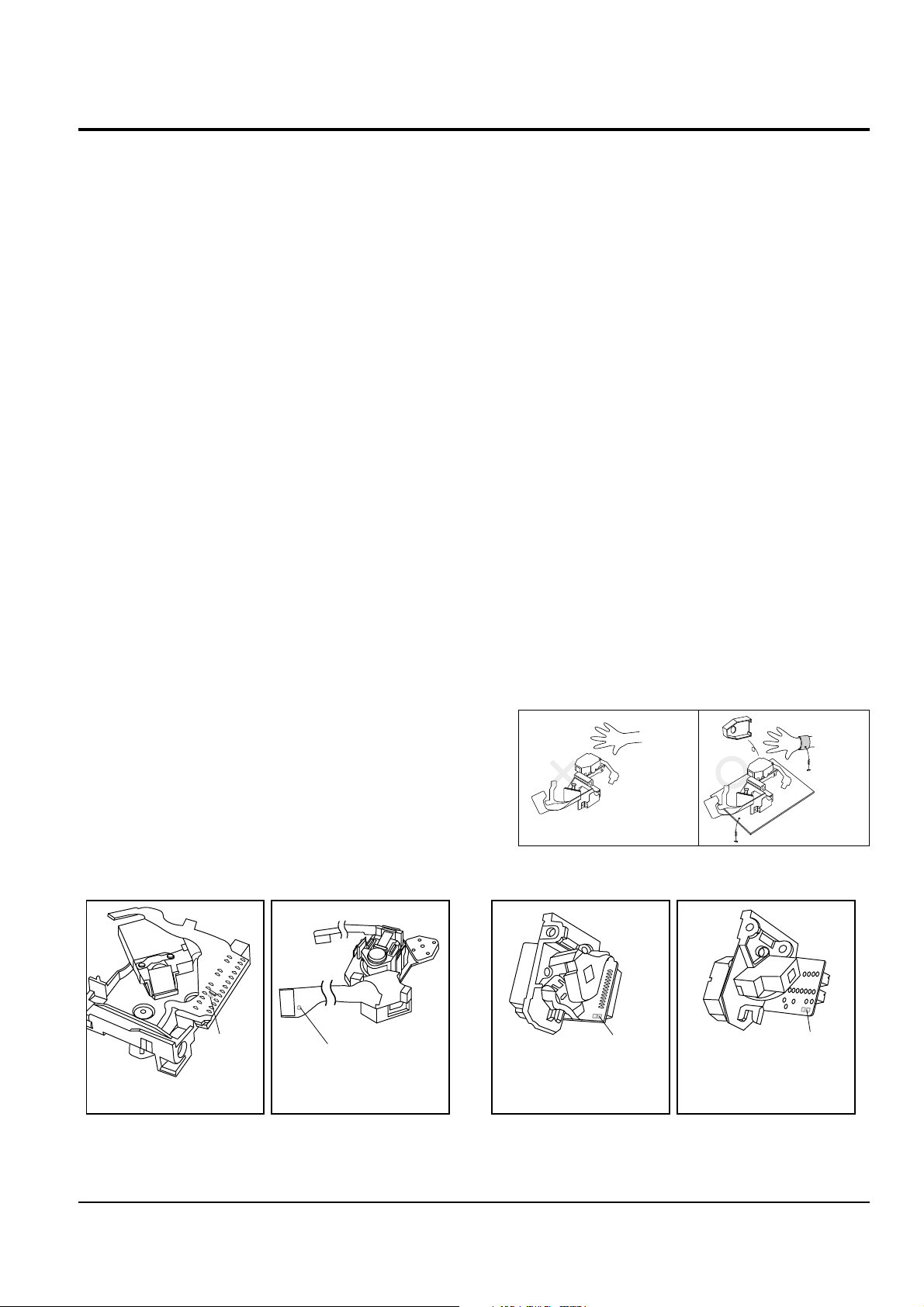
1-4-3 Handling the Optical Pick-up
1. Static electricity from clothing or the body
may cause electrostatic breakdown of the
laser diode in the Optical Pickup. Follow
this procedure:
2. Place a conductive sheet on the work bench
(i.e., the black sheet used for wrapping
repair parts.) Note: The surface of the work
bench should be covered by a copper
ground plane, which is grounded.
3. The repair technician must wear a wrist
strap which is grounded to the copper sheet.
4. To remove the Optical Pickup block:
Place the set on the conductive sheet, and
momentarily touch the conductive sheet
with both hands. (While working, do not
allow any electrostatic sources--such as
clothes--to touch the unit.)
5. Ground the "Short Terminal" (located on the
PCB, inside the Pickup Assembly) before
replacing the Pickup. This terminal should
be shorted whenever the Pickup Assembly
is lifted or moved.
short
terminal
SOH91VI(LDP)
short terminal
SOH91CI(CAR,walkman)
6. After replacing the Pickup, reopen the Short
Terminal. See diagrams below:
1M
THE UNIT
(1) WRIST-STRAP
FOR GROUNDING
short
terminal
SOH-A1
(CMS-V10,CMS-V30)
1M
SOH94T4N
(CMS-V10,CMS-V30)
CONDUCTIVE SHEET
short
terminal
Samsung Electronics1-4
Page 6
2. Product Specifications
Power source
Power consumption
Dimensions (mm)
230V
247W
270(W)x317(H)x333(D)
Power output
Total harmonic distortion
Frequency range
Signal to noise ratio
Channel separation
Input sensitivity
Frequency range
Usable sensitivity
Signal to noise ratio
Middle frequency
Total harmonic distoration
Separation (Stereo)
Frequency range
Usable sensivity
Signal to noise ratio
Middle frequency
Total harmonic distortion
Frequency range
Usable sensivity
Signal to noise ratio
Frequecny range
WOW FLUTTER
Erasing effect
Signal to noise ratio
Total harmonic distortion
Frequency response
Signal to noise ratio
Channel separation
Total harmonic distortion
87.5 ~ 108MHz
1µV
62dB
60dB
0.45%
35dB
522 ~ 1611KHz
600µV
40dB
30dB
2%
146 ~ 290KHz
1000µV
35dB
125Hz ~ 12.5KHz
0.15%
60dB
40dB
2.5%
20Hz ~ 20KHz(¡ 1dB)
90dB(1kHz 0dB)
80dB(1kHz 0dB)
0.05%(1kHz 0dB)
65W/CH(6½)
10%
30Hz ~ 25kHz
75 dB
50 dB
400mV
General
Amplifier
Tuner
Cassette
Compact Disc
FM
MW
LW
Samsung Electronics 2-1
* Specifications are subject to change without notice.
Page 7
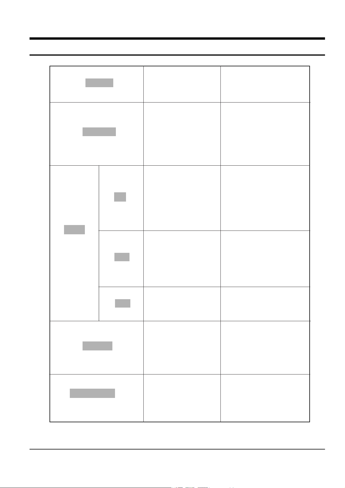
3. Disassembly and Reassembly
3-1 Cabinet-Top
1. Remove 11 screws holding the cabinet-top.
2. Lift the back of the cabinet-top and slide it to the rear to remove. (See arrow)
Samsung Electronics 3-1
Fig. 3-1
Page 8
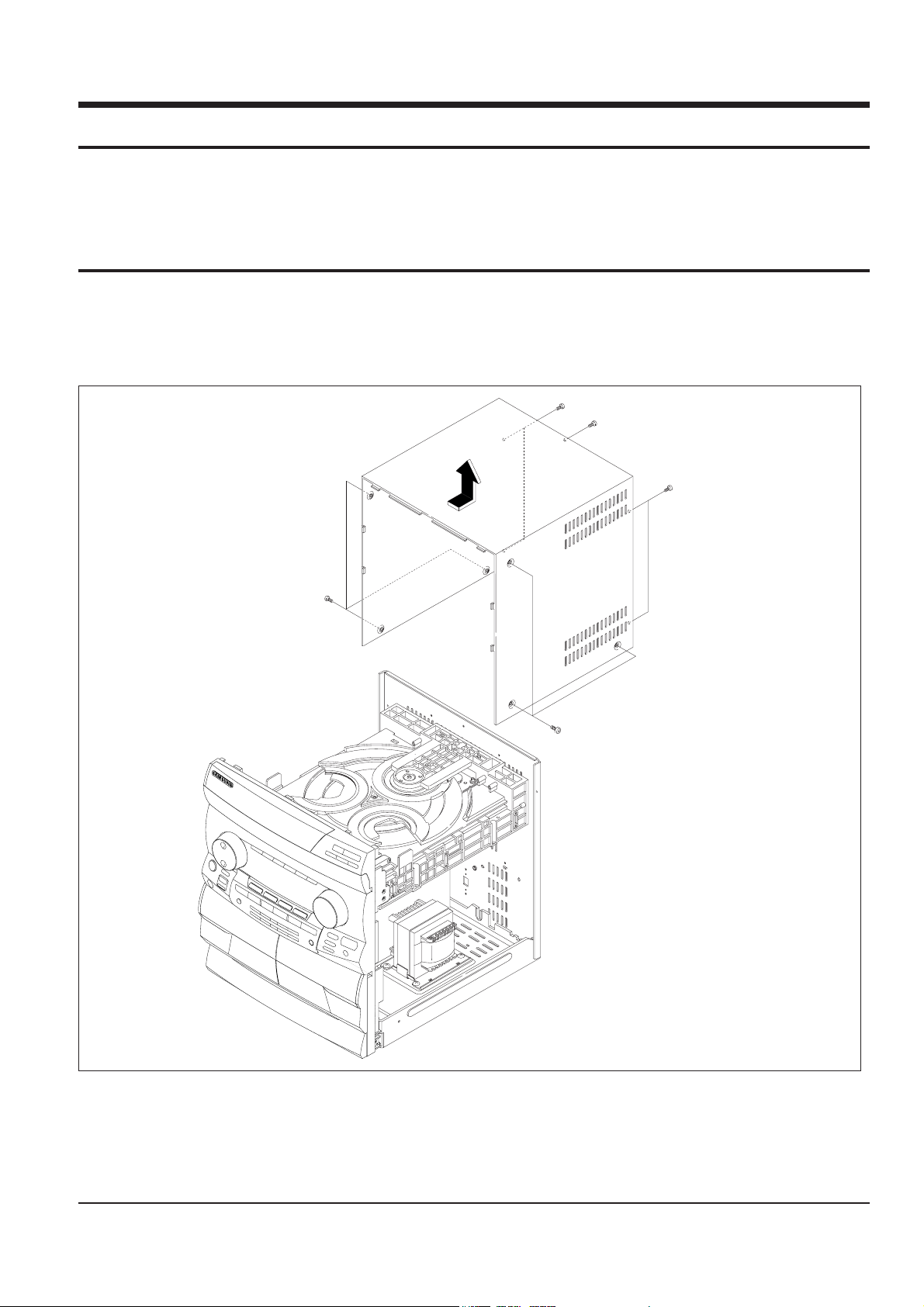
3-2 CD-Mecha, DOOR-CD
1. If power is connected :
- Turn power on
- Open the tray using the open/close key
- Remove the Door in the direction of arrow #.
2. If Power is not connected :
- Turn the gear clockwise using a screw driver as shown in Fig. 3-1- 1.
- Pull the Tray in the direction of arrow @ and then remove the Door in the direction of arrow # .
3. Remove 2 screws $ and lift the CD-Mecha.
1
2
3
4
4
3-2 Samsung Electronics
Fig. 3-2-1
Fig. 3-2
Page 9
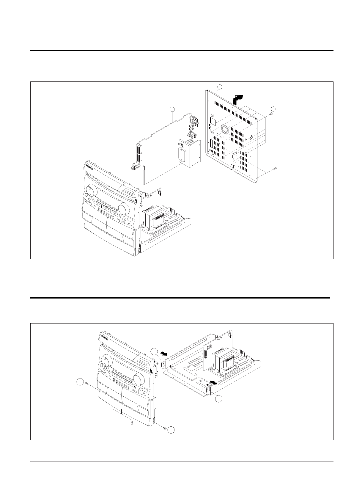
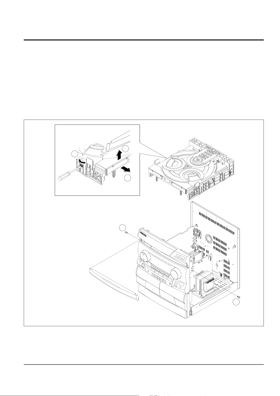
3-3 Cabinet-Rear and Main PCB
3-4 Cabinet-Front and Cabinet-Bottom
1. Remove 11 screws % and then lift the cabinet-rear ^ and slide it to rear to remove (see arrow).
2. Remove the Main-PCB & to rear.
7
6
5
1. Remove 5 screws *.
2. Remove the cabinet-rear by pushing the "A" and "B" as shown.
Samsung Electronics 3-3
Fig. 3-3
Fig. 3-4
A
8
8
B
Page 10
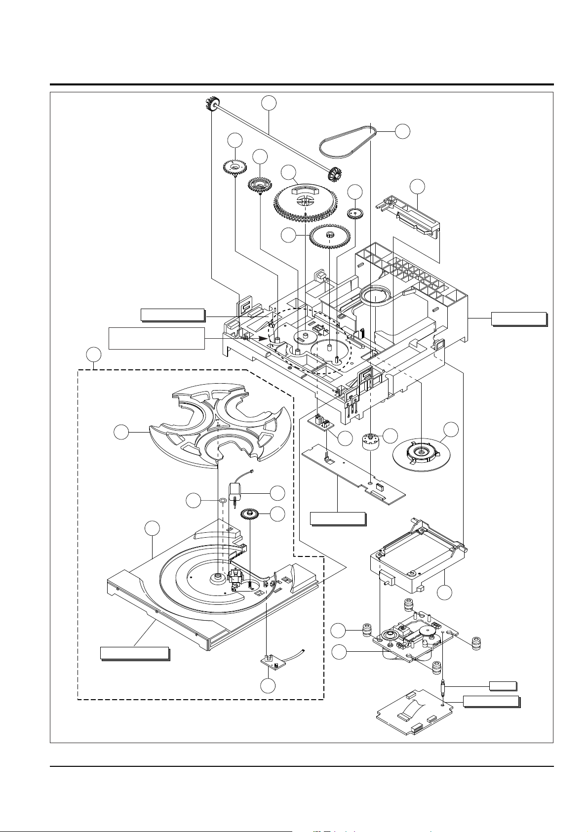
3-5 CD Mecha
3-4 Samsung Electronics
Fig. 3-5
1313
88
22
77
66
55
44
99
33
11
1010
1717
1616
1212
1111
2020
1515
2121
1414
1919
CD SUB PCB
TRAY DISC ASS'Y
TRAY STOPPER
CD MAIN PCB
HOOK
BASE MAIN
1818
Refer to the next page
for timming point
Page 11

3-5 CD Mecha Continued
Samsung Electronics 3-5
3-5-1 Tray Disassembly
3-5-2 Main Disassembly
3-5-3 CD Main PCB Disassembly
1. Remove the Tray-Roulette (3) from the Tray-Disc AssÕy (4) by releasing the hook.
2. Remove the PCB-Sensor AssÕy (5) from the tray by releasing the hook.
3. Remove the Worm-Motor AssÕy ()) from the Tray-Disc AssÕy (4).
4. Remove the Cushion-Motor (1) from the Tray.
5. Remove the Gear-Roulette (2) from the Tray-Disc AssÕy (4) by releasing the hook.
* When removing, take extreme care not to damage the hook.
1. Open the Tray Disc AssÕy by turning the Gear-Load (%) in the direction of open, then remove the
Wire-Tray (Q) .
2. Remove two Tray-Stopper and tray.
1. Remove the Table-Chuck AssÕy (6) from the Base-Main by turning it.
2. Push the Slider-Cam (!) towards right, then lift it up to remove.
3. Remove the Gear-Tray (^) from the Base-Main by releasing the fixed hook.
4. Remove the Gear-Converter (&) from the Base-Main by releasing the fixed hook.
5. Remove the Gear-Cam (%) from the Base-Main by releasing the fixed hook.
6. Remove the Belt (@) from the Pulley-Motor AssÕy (7) & the Gear-Pulley (#).
7. Remove the Gear-Pulley (#) from the Base-Main by releasing the fixed hook.
8. Remove the Gear-Load ($).
9. Remove the Gear-Synchro (*).
10. Desolder two soldering points of the CD SUB PCB, then remove it from the Base-Main by releasing
the hook.
11. Remove the Pully-Motor AssÕy (7) by releasing the hook.
12. Remove the PCB-SW AssÕy (8) by releasing the hook.
1. Remove the Lever-Lifter (9) from the Base-Main by releasing two hooks.
2. Remove four Rubber-CD (0) from the Lever-Lifter and then remove the Deck-CD (“).
3. Remove the Hook .
4. Remove the CD Main PCB with the soldering iron.
Page 12
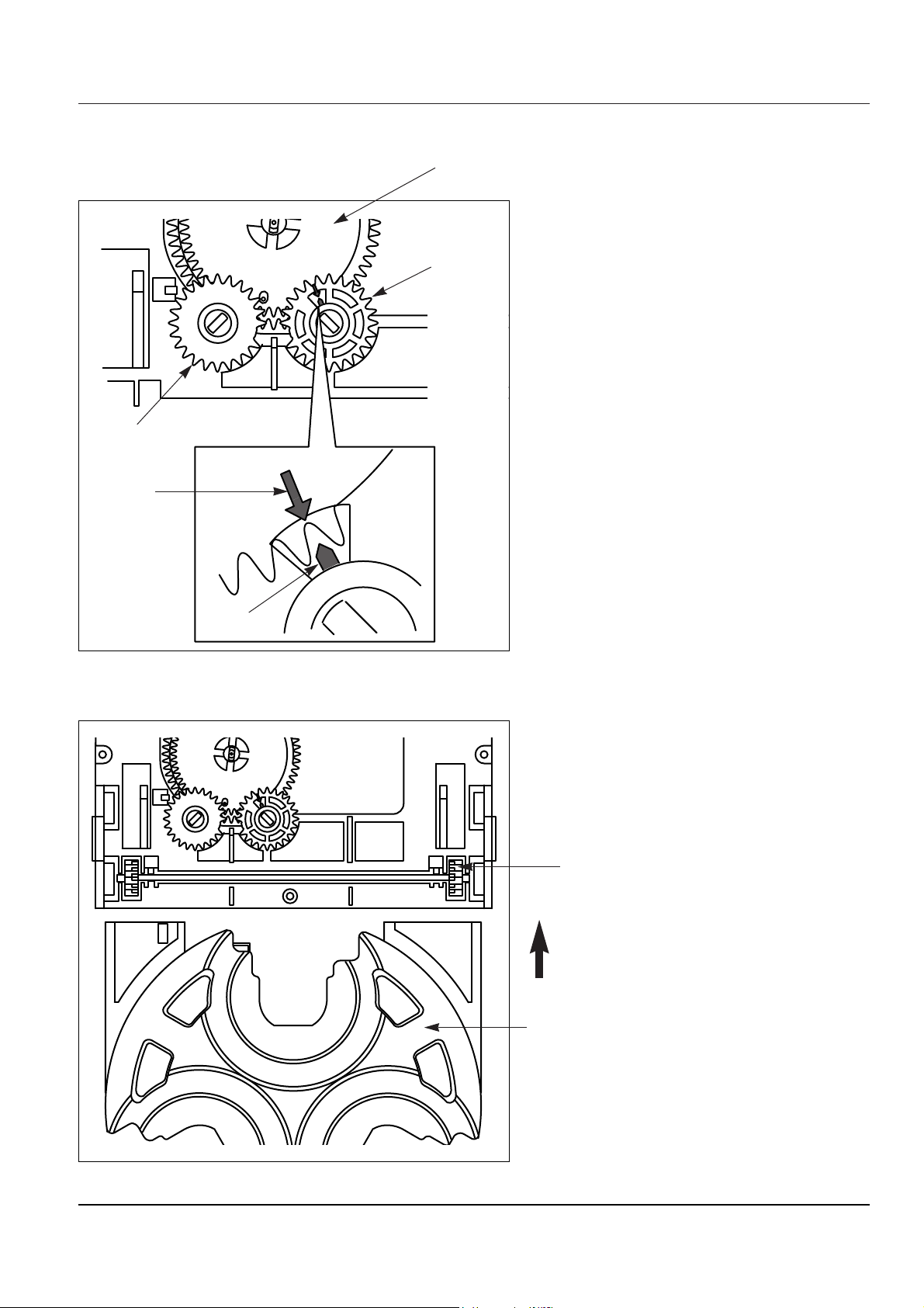
3-6 Samsung Electronics
Fig. 3-7
Fig. 3-6
Gear-Cam
Gear-Cover
Gear-Cam
Gear-Synchro
Gear-Disc
Insert
Gear-Tray
* Reinstall in reverse order.
* Align the Gear-cam with the gear-Tray as
shown in Fig.3-6, then mount the Tray-Disc.
* When assembling the Tray-Disc, take extreme
care not to engage with Gear-Synchro.
Gear-Cam
Timming Point
Disassembly and Reassembly
Page 13
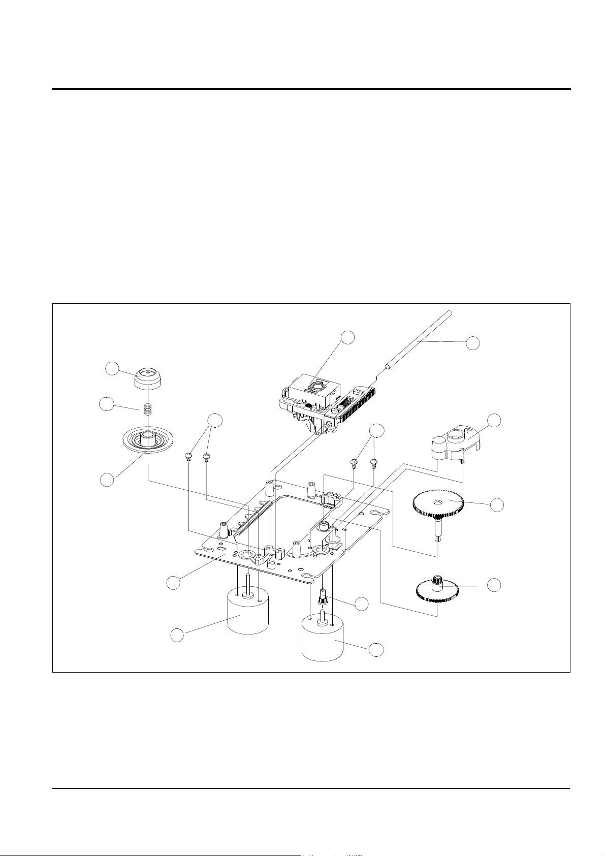
3-6 CD Deck
1. Remove the Shaft ! .
2. Lift the P/U @ .
Note : Take extreme care not to touch the surface of lens.
3. Lift the Center-ring # .
4. Remove the Spring-T/Table $ .
5. Remove the Turn-Table (M) % .
6. Remove 2 screw ^ and then remove the Spindle-Motor & .
7. Remove the Cover-Gear * by pushing the hook.
8. Remove the Gear(c) ( by pushing the hook.
9. Lift the Gear(b) ) .
10. Remove the Gear(a) 1 .
11. Remove 2 screws 2 and then remove the Feed-Motor 3 .
12. Remove the Chassis-Deck(M) 4.
3
4
5
6
12
2
1
8
9
10
11
13
14
7
Samsung Electronics 3-7
Fig. 3-8
Page 14
4-1Samsung Electronics
4. Alignment and Adjustments
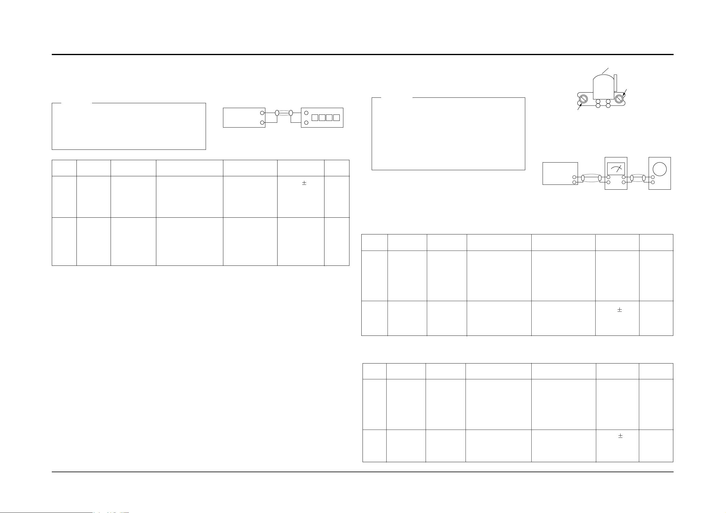
4-1 Tuner
FM T.H.D Adjustment
SSG FREQ. 98MHz
Adjustment
point FM DETECTOR COIL
(IFT6)
Minumum output(Fig.1)
FM Search Level Adjustment
SSG FREQ. 98MHz
Adjustment
point SEMI-VR(5KB)
(MSR1)
"TUNED" is shown on FLT(Fig.2)
FM
Antenna
Terminal
Speaker
Terminal
Input
Input
Fig.1 IF CENTER and T.H.D Adjustment
Fig. 2 FM Auto Search Level Adjustmet
Output
Distortion Meter
Oscilloscope
FM SSG
FM SSG
GND
30 dB
75½
Dummy
FM IN
FM Antenna
SET
5 k½
SET
Output
GND
DSR4L
1-PLAY
DSR3L
2-PLAY
DSR2L
REC
DSR5
SPEED
DSR1L
DSR1R
BIAS
BIAS OSC FREQ.
LL3
IFT6
FM T.H.D
MSR1
FM TUNED
Page 15
Samsung Electronics4-2
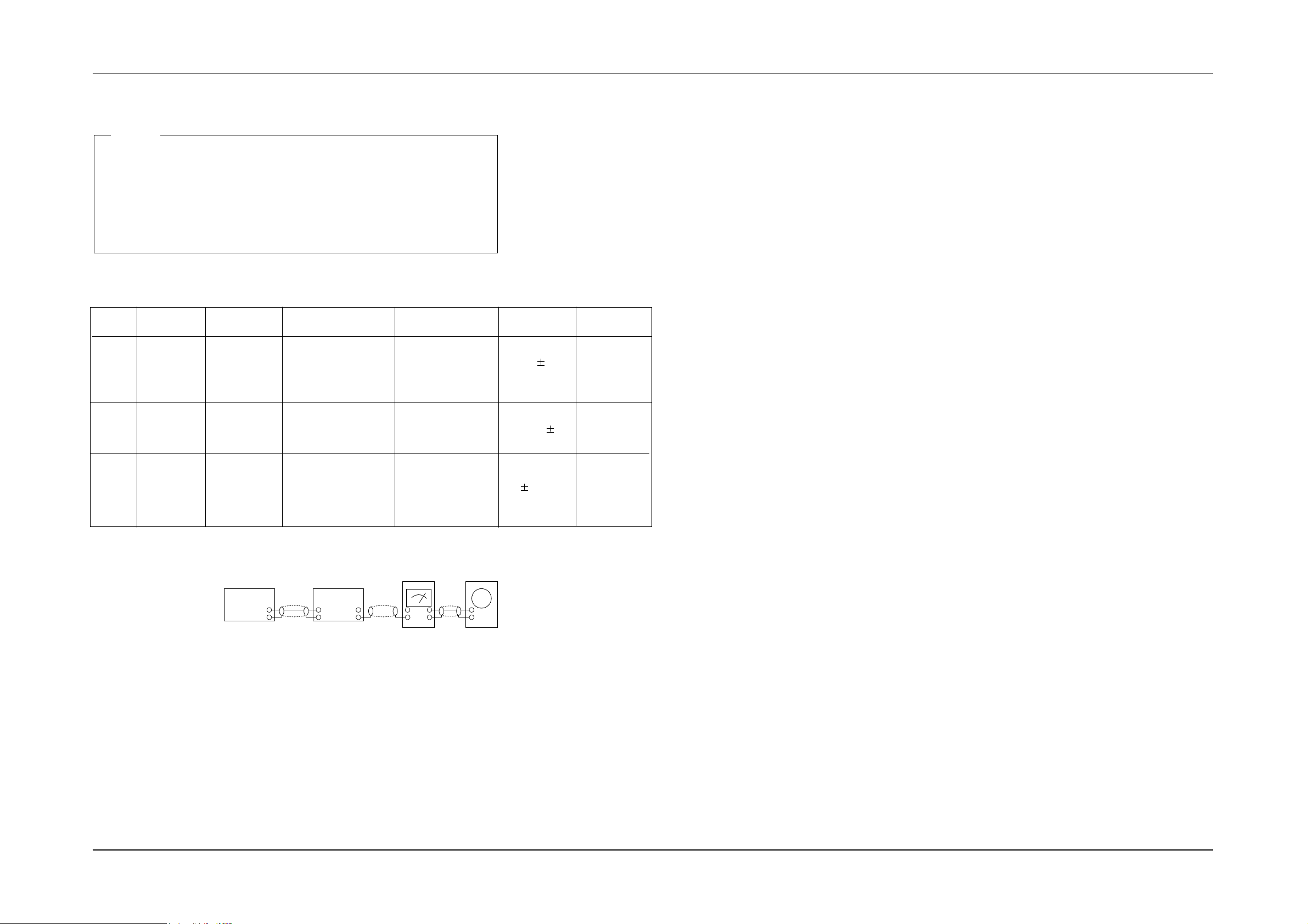
4-2 Cassette Deck
1) Measuring tape: i) MTT-111 (or equivalent)
(Tapes recorded with 3KHz)
ii) MTT-5512 (or equivalent)
2) Connect the cassette deck to the frequency counter
as in Fig. 1.
NOTES
4-2-1 To Adjust Tape Speed
1) Before the actual adjustment, clean the replay/recording
head.
2) Measuring tape :
i) MTT-114NA (or equivalent 12.5 kHz AZIMUTH
control).
ii) MTT-150 (or equivalent : Dolby level 200mwb/m)
3) Dolby NR SW OFF
4) The cassette deck is connections as shown in fig. 3.
NOTES
4-2-2 To Adjust Replay Head
NOR
SPEED
Control
counter
HI SPEED
Control
OUT
(connected
to the frequency
counter)
Same as above
1) A-Deck: MTT-111
2) Press PLAY SW button
3) B-Deck: Same as below
1) A-Deck: MTT-111
2) B-Deck: MTT-5512
3) Press Hi Speed
dubbing switch
Turn DSR5 to
left and right.
Fixed
3KHZ 1%
5700~6300KHz
Check
1
2
Step
Step
Step
To Adjust
To Adjust
To Adjust
Item
Item
Item
Standard
Standard
Standard
Remark
Remark
Remark
Pre-Setup
Condition
Pre-Setup
Condition
Pre-Setup
Condition
Pre-Setup
Pre-Setup
Pre-Setup
AZIMUTH
PlayBack out
Level
TP3 OUT
(VTVM is
connected
to the scope)
Same as
above
After putting MTT
-114NA into Deck 1.
1) Press FWD
PLAY button.
2) Press REV
PLAY button.
PLAY MTT-150
on Deck1.
1)Turn the control knob to
as shown in Fig.2.
2) Adjust the right
control screw to
playback Rev. Mode.
L-CH :Turn DSR3Lto
the right and left
R-CH : Fixed
Max output
and same
phase (both
channels).
100mV 0.5dB
After
adjustment
secure it
with
REGION
LOCK.
See the
diagram
for
adjustment
locations
After
adjustment
secure it
with
REGION
LOCK.
See the
diagram
for
adjustment
locations
1
2
AZIMUTH
PlayBack
out Level
TP3 OUT
(VTVM is
connected
to the scope)
Same as
above
After putting MTT
-114NA into Deck 2.
1) Press FWD
PLAY button.
2) Press REV
PLAY button.
PLAY MTT-150
on Deck2.
1)Turn the control knob
to left and right as shown
in the Fig.2.
2) Adjust the right
control screw to
playback Rev. Mode.
L-CH :Turn DSR4L to
the right and left
R-CH : Fixed
Max output
and same
phase both
channels.
100mV 0.5dB
1
2
¤ Adjust 1-Deck Replay Level
¤Ł Adjust 2-Deck Replay Level
Fig. 1
Fig.2
Fig. 3
Cassette Deck
Oscilloscope
Recording/Play head
REVERSE
PLAY
In Out
AZIMUTH control knob
Cassette Deck
Frequency Counter
LINE OUT
TP3
Output
LINE OUT
TP3
(GND)
VTVM
V H
Page 16
LINE OUT
IN
VTVM
AUDIO OSC
TP1 TP
VTVM
400mV 5%
105KHz 5%
VTVM
(7V 5%)
4-3Samsung Electronics
Alignment and Adjustments
1) Connect the measuring instruments as shown in Fig. 4.
2) Set the DOLBY NR Switch off.
3) Measuring tape :
MTT-5512 ( or equivalent : normal recording )
4) The input signals supply 400Hz 400mV into AUX IN of AMP (AUDIO OSC).
NOTES
Step
Item
Pre-Setup
Condition
Normal
electric
current for
recording
BIAS OSC.
FREQUENCY
BIAS electric
current
Connect to TP2
as in Fig. 4 and
read VTVM
Connect the
frequency
counter to TP
Connect to
TP1 as in Fig.4
and read the
VTVM
Insert MTT-5512 into
Deck 2, then press
REC button.
Insert MTT-5512 into
Deck 2, then press
REC button.
Insert MTT-5512 into
Deck 2, then press
REC button.
L-CH : DSR2L to
the right and left.
R-CH : Fixed
Turn BIAS oscillator frequency coil
(LL3) to the right
and left.
L-CH : DSR1L and
R-CH: DSR1R to
the right and left.
See diagram for
adjustment
locations.
See diagram for
adjustment
locations.
See diagram for
adjustment
locations.
1
2
3
4-2-3 To Adjust PlayBack
Fig. 4
In Out
Oscilloscope
Cassette Deck
AUX IN
Pre-Setup
To Adjust
Standard
Remark
Page 17
Samsung Electronics4-4
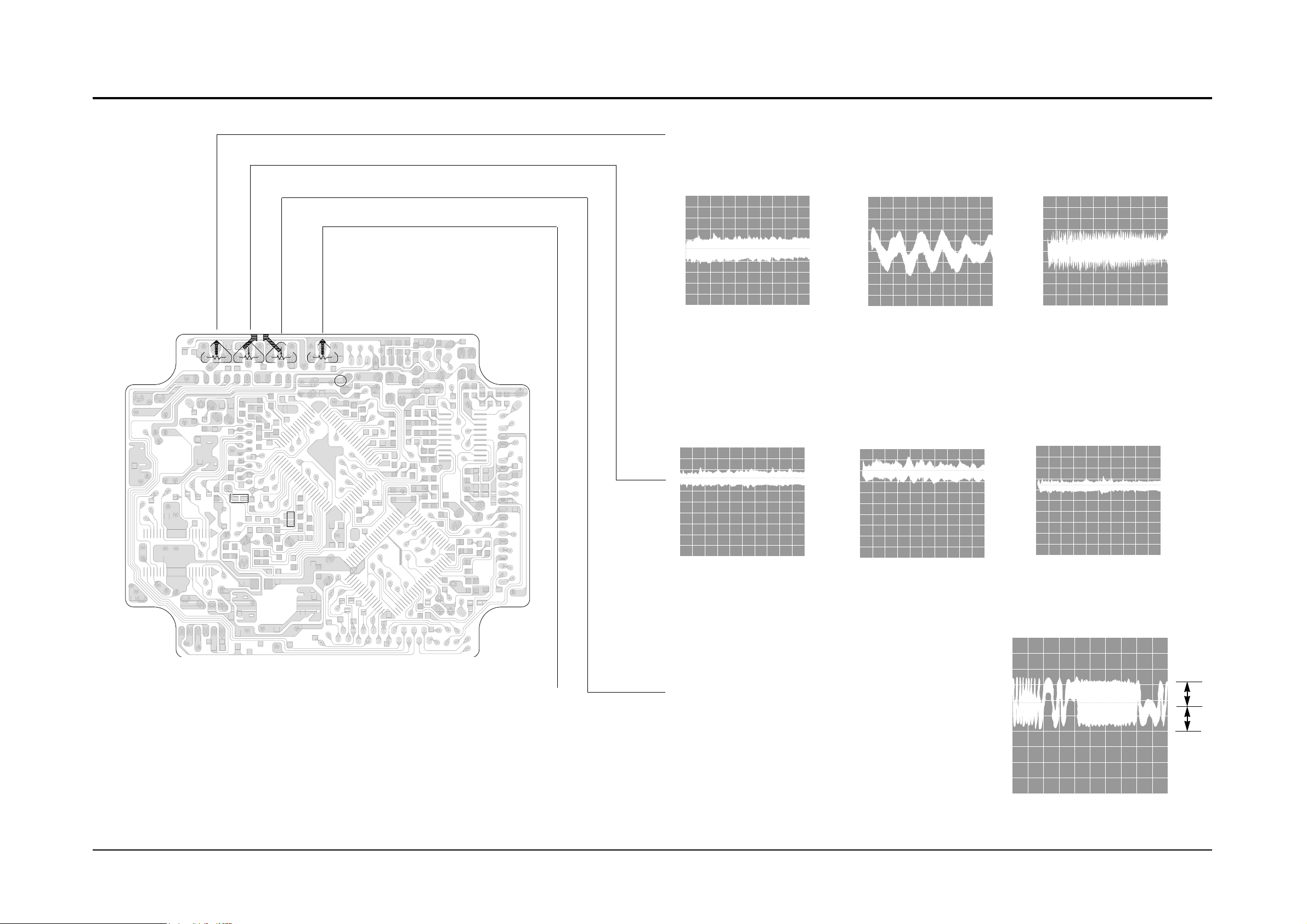
4-3 CD
TP2
TP1
Vref
NVR1703 NVR1702
NVR1701
TE CENTER
FE CENTER
E.F BAL
F.BIAS
NVR1704
0V
A
B
A=B
---100mV
---0V
---250mV
---0 V
---100mV
---0 V
---0 V
---0 V
---0 V
4-3-1 To Adjust FOCUS BIAS(STOP mode)
4-3-3 To Adjust Focus Gain (PLAY mode)
4-3-2 To Adjust Tracking Gain (PLAY mode)
4-3-4 To Adjust E/F Balance (PLAY mode)
1. Set Volt/Div of the oscilloscope to DC 100mV.
2. Ground the scope input and set the waveform to 0V, DC range.
3. Connect the GND terminal of the oscilloscope to
VR, and (+) terminal to center of TP1.
4. Set NVR1701 to 0mV.
1. Connect the GND terminal of the oscilloscope to VR and (+) terminal to TP2.
2. Load and play the disc
3. While the disc is running adjust the gain with NVR1704 as shown below.
1. Connect the GND terminal of the oscilloscope to VR and (+) terminal to TP1.
2. Load and play the disc.
3. While the disc is running adjust the gain with NVR1703 as shown in the following figure.
VOLT/DIV : 0.2V
TIME/DIV : 2mS
Normal frequency
Normal frequency
Low frequency
High frequency
Low frequency
High frequency
VOLT/DIV : 0.1V
TIME/DIV : 2mS
VOLT/DIV : 0.1V
TIME/DIV : 2mS
VOLT/DIV : 0.1V
TIME/DIV : 2mS
VOLT/DIV : 0.2V
TIME/DIV : 2mS
VOLT/DIV : 0.2V
TIME/DIV : 2mS
1. Set TIME/DIV of the oscilloscope to 2mS.
2. Set Volt/DIV of the oscilloscope to 0.5V.
3. Ground the scope input and set to DC.
and then set the DC range.
4. Connect the GND terminal of the oscilloscope to VR
and (+) terminal to center to TP2.
5. Load and play the disc.
6. Turn NVR1704 counterclockwise to the minimum value.
7. Raise NVR1702 and adjust the waveform so that its middle
comes to GND of the oscilloscope (or until the upper half
of waveform becomes symmetrical to the bottom half, A=B)
8. Adjust NVR1704 (arrow) for normal sound.
Page 18
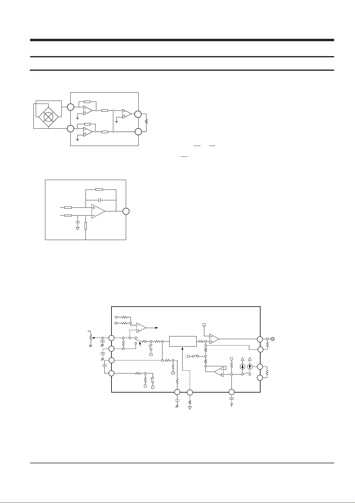
RF I-V Amp(1) and RF I-V Amp(2) are converted to voltage via
internal resistance of 58k½ from the current of PD1(A+C) and PD2(B+D):
This voltage is added to RF summing amplifier.
The signal (A+B+C+D) is applied to RFO (No. 2 terminal).
RF output voltage is calculated as follows :
VFE = (R2/R1) x (V2-V1) = 5.4(V2-V1)
This FOCUS ERROR voltage is sent to FOCUS SERVO .
VRF = -R3 x (iPD1 + iPD2)
VRF = -R3 x (V1/R1 + V2/R2)
VRF = -R3 x ( + )
VRF = - x (V1 + V2)
10K 10K
V 1 V 2
10K
R3
66
Photo Detector
B
CA
D
PD1
PD2
58K
RF I-V AMP(1)
58K
10K
R2
RF I-V AMP(2)
V2
R1
10K
RF SUMMING
V1 AMP
RFO
RF
66
R3
65
74
73
5-1-1 RF Amp (KA9220) : NIC9220
5-1-2 FOCUS ERROR Amp(KA9220) : NIC9220
59
R2
174K
C1 25P
FE
FOCUS
ERROR
AMP
164K
32K
C2 25P
-(A+C)
-(B+D)
R1
V1 32K
5-1-3 FOCUS SERVO SYSTEM (KA9220) : NIC9220
When FS3 is ON, high frequency gain decreases (time constant set by pin17, pin19, and capacitor connected
to internal resistance).
The capacitor between pin 18 and GND sets the time constant to pass the low frequency operated in PLAY mode.
The maximum frequency of focus phase compensation is inversely proportional to the resistance connected to
pin 7. Focus search peak is about 1.1 Vp-p, and is inversely proportional to the resistance connected to pins 22,23
(if this resistance changes, the peak of track jump and sled kick change).
The inversion input of FZC comparator is set to 5.7% of the difference between Vcc and VC(pin69) {{5.7% x (Vcc-Vc)}.
Note : If the resistance connected to pin7 changes, the phase compensation peak of focus, tracking, sled servo changes.
At the same time, 'op-amp' dynamic range and offset voltage also change.
3.6K
20
21
47
48
60K
FZC
0.0022
20K
0.1UF
0.1UF
FDFCT
HFGD
EFR
FE2
470K
DFCT
FS4
20K 48K
58
60
62
46K
580K FS3
FSW
470K
130K
0.1UF
27
40K
6
PFSET
FS2
PHASE
COMPENSATION
92K
40K
10K
3
4.7UF
FSCH
FS1
50K
5.5U 11U
VREG
180K
ISET
FCE
120K
FOCUS
COIL
FSEO
FE1
61
Samsung Electronics 5-1
5-1 CD
FOCUS ERROR Amp is the circuit which amplifies the difference
between RF I-V Amp(1) output (A+C) and RF I-V Amp(2)
output(B+D).
These two signals are supplied to (-) and (+) input terminals of
FOCUS ERROR Amp. The FOCUS ERROR signal resulting from this
difference voltage is applied to FE (Terminal No.57).
The FE output voltage of this low frequency component varies
according to {(A+C) - (B+D)}.
VFE is calculated as follows :
5. Special Circuit Descriptions
Page 19
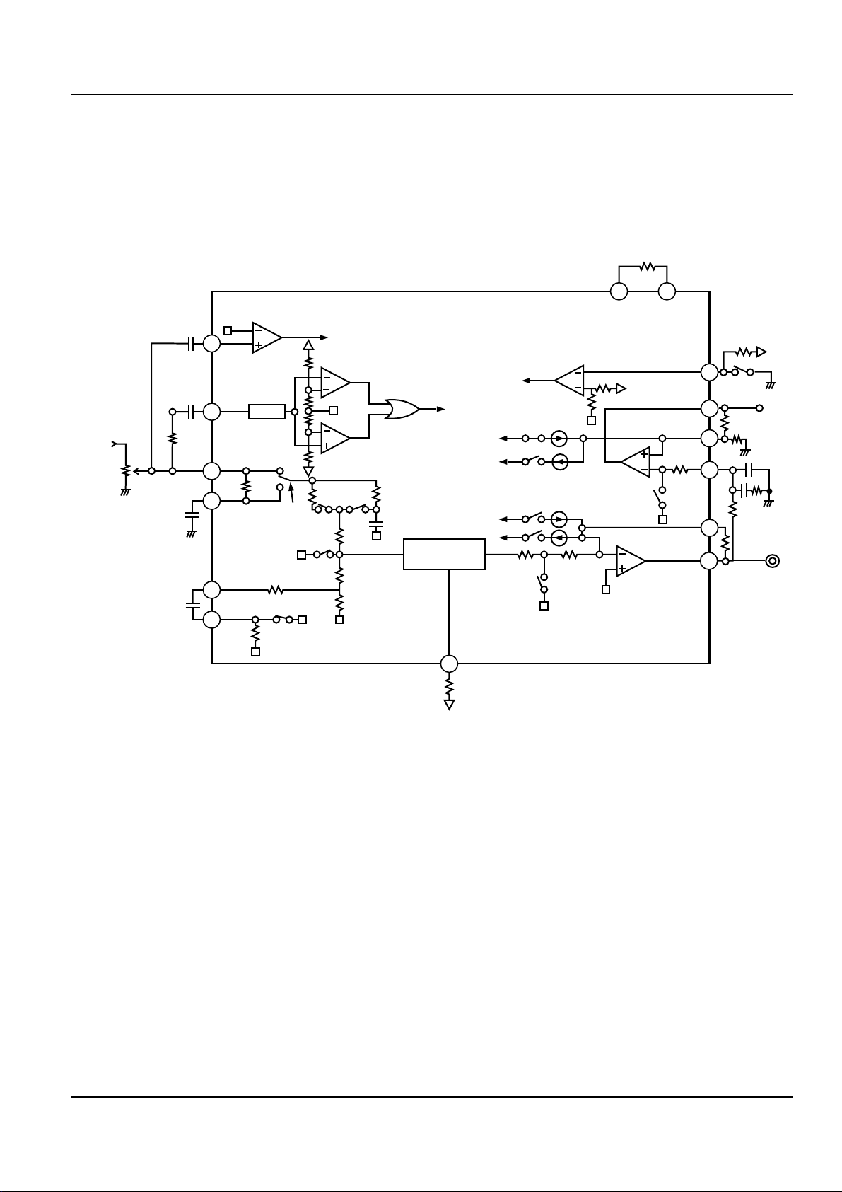
5-1-4 TRACKING SLED SERVO SYSTEM (KA9220) : NIC9220
The capactor between pin 15 and 16 attenuates the high frequency when TG2 is off. The maximum frequency of
tracking phase compensation is inversely proportional to the resistance connected to pin 7 (about 1.2kHz at 470k).
The tracking jump (FWD and REV) is decided when TM3 and TM4 are ON, and the peak voltage induced from
tracking coil is decided by the both TM3 and TM4 current values and feed back resistance of pin 47.
Track jump max voltage = TM3 (TM4) current x feedback resistance.
FWD or REV sled kick occnrs when TM5 or TM6 is ON, and the peak voltage added to sled motor is decided by
TM5 or TM6 current and the feedback resistance of pin 41.
Sled jump max. voltage = TM5(TM6) current x feedback resistance
Each SW current is decided by the resistance connected to pin 22 and 23.
When the resistance is about 150½,
TM3 or TM4 = 11µA,
TM5 or TM6 = 22µA,
This current is inversely proportional to the resistor, variable within a range of t 5 to 40 µA for TM3.
STOP is the ON/OFF detection signal for the limit SW (or the sled motor's innermost cirumference).
22 23
40
41
39
47
48
7
15
16
54
52
50
51
0.022UF
TZC
0.047UF
150K
BPF
1K
1K
TZC
100K
ATC
20K
TE 1
TE2
470K
100K
ATS
TDFC1
0.1UF
680K
66PF
10K
DFCT
0.1UF
RTG
20K
TGSW
470K
TG2
82K
110K
PHASE
COMPENSATION
S STOP
1K
100K
S STOP
SLED
SLEI
SLEN
10K
56K
100K
ISET VREG
180K
SLED
DRIVER
120K
100K
TKEO
TKEI
TM2
TM6
TM5
TM4
5.5U
TM3
5.5U
10K
90K
TM7
PFSET
470K
8
TRACK
COIL
5-2 Samsung Electronics
Special Circuit Descriptions
Page 20

6. Troubleshooting
6-1 Amplifier
6-1-1 Power Malfunction
Samsung Electronics 6-1
O
Check voltage of NIC05 : 5V
X
O
Check waveform of NIC9282
pin no. 19,20
X
Check NIC9282 soldering
O
Check waveform of NIC9270
pin no. 9,12
X
Replace NIC9270
Check NIC9270 soldering
O
Replace NIC05
Check Amp
Malfunction of Audio Output
Page 21

6-2 Samsung Electronics
Troubleshooting
O
AQ1L/1R Base B+ ?
O
Is Mute selected ?
O
Headphone Jack short ?
FIC3 (NJU3718) pin no.27
Check the "H" ?
Remove it with Remocon
Replace Headphone jack
soldering condition
Replace FIC3(NJU3718)
Main PCB AIC1(STK4191V)
pin no. 8,9,11,12,14
B+,B- circuits
Check the B+ power
source part in RD1(PBL403),
RC4 and RC5.
O
Confirm for TR short
replace it.
Check if the output line is
short.
O
X
X
X
X
X
6-1-2 No Output
Page 22

Samsung Electronics 6-3
Troubleshooting
MZD2 Voltage ok ?
O
Check TUNER IC(LA1836)
pin no.10 ; 8.6V
pin no.14 ; 7.2V
AM ; 0V ?
MZD1 (5.6V) Voltage ok?
MIC2 (LC72131) FM/AM BAND
Switching ok?
X
O
LC72131
CONTROL ok?
O
FM VT
LC72131 pin no.20
1.7V 7.5V ?
O
AM VT
LC72131 pin 20
Check the LC72131
CONTROL ok ?
O
O
Check MIC2
pin 20 ?
LPF(MLPF 1L/1R)
output ok?
Check TDA7318 function ok?
Check FEP interior
pattern, and any line
disconnections.
1) Power settion
defective ?
2) LC72131 Oscillator
(HX1 : 7.2MHz) ok ?
3) System line ok?
X
O
Check for µ-com IC
Replace LC72131
X
X
X
X
X
X
X
O
0.9V 7V
?
Check MZD2 (8.2V), MR29
6-1-3 Tuner Malfunction (FM/AM)
Page 23

6-4 Samsung Electronics
Troubleshooting
O
Connector inserted
correctly?
X
O
Check voltage : AC 4.8V
at FRONT-PCB FLT?
X
Check Main-PCB Front PCB
connection and the voltage of
CCW1, pins1,2(AC4.8V)
O
Check voltage at UIC1
pin no. 48(-33V)
X
Check the voltage of RZD1(-33V)
Reinsert the connector.
Replace UIC1
6-1-4 V.F.D Malfunction
Page 24

Samsung Electronics 6-5
6-2 Cassette Deck
Block Main Function Check Point
TAPE IC JIC1
(BA3442AKS)
Convert of P/B & R/P SIGNAL &
DECK OUTPUT OF IC
Check for voltage at PIN32
1 P/B Deck : L
2 R/P Deck : H
Check for pin24 of FIC3 when deck operate
Check for voltage at pin28
When between song : High (Normal)
When playing song : Low (Normal)
AMPS
DOLBY NR AMP
DIC1 (KA2271)
Convert P/B & SOURCE SIGNAL
Convert DOLBY NR ON/OFF
Oscillate RECORD BIAS (105KHZ)
Oscillate RECORD BIAS (105KHZ)
DQ1,1R, Gate check
Check for RESET
When power is turned ON.
Check VF DISPLAY
Drive VF DISPLAY
VF DISPLAY
µ-com UIC1
Control DECK MECHA
Control VF DISPLAY
Control MUTE circuit
Control each circuit
TP2 check
Osc Frequency : 105KHz
When inoperative : LQ4,LQ5 check
BIAS OSC
DIC1 pin13 check
Check for voltage at pin4
R/P mode : High
R/p mode : Low
Dubbing mode : High
When in operative FIC3 pin 26 check
Mode FIC3 pin12
P/B H
R/P L
DUBBIN H
Mode FIC3 pin25
OFF H
ON L
Mode DQ1L/1R
REC -10V
PLAY 1.4V
Page 25

6-6 Samsung Electronics
O
Check Deck down
X
O
Check CLOSE S/W voltage.
CLOSE condition: 0V
X
Check CLOSE MOTOR
and CLOSE S/W.
O
Does Roulette revolve ?
X
Check Roulette Motor.
O
Is Roulette Control ok ?
X
Check Roulette Control Sensor
O
Is Focus Search ok ?
X
Check oscillation of NXF100
(16.9344MHZ)
O
Does Laser function during
Focus Search ?
X
Replace PICK UP
Replace NIC9220 or NIC9258
O
POWER ON
Check UP/DOWN MOTOR
X
Replace NIC9282
O
Check NIC9282 pin73 voltage
during Focus Search
: 5V
6-3 CD
6-3-1 Disc Revolution Malfunction
Page 26

O
Check voltage of NIC05 : 5V
X
O
Check waveform of NIC9282
pin no. 19,20
X
Check NIC9282 soldering
O
Check waveform of NIC9270
pin no. 9,12
X
Replace NIC9270
Check NIC9270 soldering
O
Replace NIC05
Check Amp
Malfunction of Audio Output
Samsung Electronics 6-7
Troubleshooting
6-3-2 Audio Output Malfunction
Page 27

7-1Samsung Electronics
7. Exploded Views and Parts List
7-1 Cassette Deck Exploded View and Parts List
1
2
4
4
5
6
7
7
9
10
20
22
24
25
26
27
28
29
11
13
14
15
17
18
19
16
24
26
12
3
4
5
6
7
7
9
10
21
23
25
27
30
11
16
13
14
15-A
17
18
19
4
12
28-A
No. New Code No. Description Specification Old Code No.
1
2
3
4
5
6
7
8
9
10
11
12
13
14
AH59-20004J
AH81-10798A
AH81-10798C
AH81-10798D
AH81-10798E
AH81-10798F
AH81-10798G
AH81-10798H
AH81-10798J
AH81-10798K
AH81-10798M
AH81-10798N
AH81-10798P
AH81-10798S
AH81-10798U
CASSETTE DECK
MOTOR ASSÕY
HEAD ASSÕY(R/P)
HEAD ASSÕY(P/B)
SOLENOID ASSÕY
CNTR ASSÕY(R/P)
CNTR ASSÕY(P/B)
FLYWHEEL ASSÕY(F)
FLYWHEEL ASSÕY(R)
PINCH ARM(F)
PINCH ARM(R)
CLUTCH ASSÕY
MAIN BELT(R/P)
MAIN BELT(P/B)
SUB BELT
ADR2112TW
SHU2L-DOUBLE
YK56RBB4N3
YK50PBB4N3
ADR2100-01
ADR2100-02
ADR2100-03
ADR2100-04
ADR2100-05
ADR2100-06
ADR2100-07
ADR2100-08
ADR2112TW-01
ADR2112TW-02
ADR2100-09
Page 28

Samsung Electronics7-2
1
3
4
5
6
7
8
9
20
30
31
32
33
34
35
36
37
38
39
40
41
42
21
22
25
25
26
26
29
11
13
14
15
16
17
18
19
43
44
45
46
47
48
49
PCB - MAIN
POWER - CORD
PCB - CD
PCB - FRONT
PCB - POWER
a
Exploded Views and Parts List
Page 29

7-3Samsung Electronics
Exploded Views and Parts List
7-2 Main Parts List and Exploded View
1
2
3
4
5
6
7
8
9
11
13
14
15
16
17
18
19
20
21
22
25
26
29
30
31
32
33
34
35
36
37
38
39
40
41
42
43
44
45
46
47
48
49
50
AH64-30351A
G3A8-3N/C
AH64-50305B
AH64-30350B
AH69-10103A
AH64-11003A
AH64-11005A
AH64-11008A
AH67-10100C
AH64-11004A
AH61-20355A
AH64-10999A
AH67-10105A
AH61-20079A
AH61-20359A
AH64-11006A
AH67-10101A
AH64-11007A
AH67-10104A
AH67-10102A
AH95-50001A
AH61-80030A
AH61-20358B
AH64-11011A
AH64-11002A
AH64-40350C
AH61-20352E
AH64-40351C
AH64-70003B
AH61-60192A
AH64-50303B
AH64-50304B
AH61-60305A
AH61-60306A
AH64-40352C
AH64-40353C
AH59-20004D
AH64-30352A
AH64-80032A
AH31-10020A
AH61-10627A
AH62-30105A
AH64-30353C
AH59-10082E
13322-0145-00
12689-0009-00
16674-518-510
17159-0093-00
A3070-0112
PVC STEEL, T0.75 MAX630
G3A8 3N CKD
ABS 94HB, BLK, MQ-630
MIPS BLK, MAX-630
PMMA, TRP+TIO2, MAX630
ABS 94HB, BLK, MAX630
ABS 94HB, BLK, MAX630
ABS 94HB, BLK, MAX630
PMMA, +TIO2, MAX630
PMMA +TIO2 MAX630
ABS 94HB WHT MAX630
ABS 94HB, BLK, MAX630
PMMA +TIO2 MAX630
ABS 94HB BLK MAX-380
ABS 94HB WHT MAX630
ABS 94HB BLK MAX630
PMMA +TIO2 MAX630
ABS 94HB, BLK, MAX630
PMMA +TIO2 MAX630
PMMA BRN MAX630
MAX555
POM, N0.8, G130,BLK,MAX630
ABS 94HB BLK MAX-630
ABS 94HB BLK MAX630
ABS 94HB BLK MAX630
PMMA, VIO,MAX-630
ABS 94HB BLK MAX-630
PMMA VIO MAX-630
AL, L30
SUS, PI0.35, COM
ABS 94HB, BLK,MQ-630
ABS 94HB, BLK,MQ-630
TS, SUS27,PI1.0 MAX-630
TS, SUS27 PI1.0 MAX-630
PMMA VIO MAX-630
PMMA VIO MAX-630
CWA420R, LOGIC
SECC, T1.0 MAX630
HH-38C T2.0 BLK MAX-630
D0620B-12M, 12VDC 10.16A
SECC T1.0 NTR MAX-630
AL T6.0 WHT MAX-630
SECC T0.8 MAX-630
MAX-630
CABINET-TOP
ASSY-CD PACK
DOOR-TRAY
CABINET-FRONT
LENS-SKIP
KNOB-OPEN/CLOSE
KNOB-DIRECTION
KNOB-POWER
LENS-AI OFF
KNOB-FUNCTION
HOLDER-FUNCTION
KNOB-ENTER
LENS-JOG
HOLDER-VFD
HOLDER-DIRECTION
KNOB-DECK
LENS-KNOB
KNOB-SBS
LENS-SRS
LENS-REMOCON
LATCH-ASSY
DAMPER-ASSY
CAP-DUMMY
KNOB-VOLUME
KNOB-JOG
WINDOW-TUNER
CAP-FRONT
WINDOW-CD
BADGE-BRAND
SPRING TAPE
DOOR-CASS, A
DOOR-CASS,B
SPRING-DOOR, L
SPRING-DOOR, R
WINDOW-DOOR, A
WINDOW-DOOR, B
DECK-CASSETTE
CABINET-BOTTOM
FOOT-CUSHION
FAN-DC
BRKT-FAN
HEAT-SINK, M
CABINET-REAR
REMOCON-ASSY
No. New Code No. Description Specification Old Code No.
Page 30

Samsung Electronics7-4
No. New Code No. Description Specification Old Code No.
7-3 CD MECHA Parts List
1
2
3
4
5
6
7
8
9
10
11
12
13
14
15
16
17
19
20
21
AH66-80022A
AH66-60034A
AH66-20186A
AH66-20187A
AH66-20188A
AH66-20189A
AH66-20190A
AH66-20191A
AH59-10097A
AH59-10098A
AH69-20044A
AH66-20193A
AH66-90056A
AH66-90055A
AH59-10099A
AH59-10100A
AH59-10101A
AH66-30086A
AH73-10016A
AJ59-20003F
SLIDER-CAM
BELT-LOAD
GEAR-PULLEY
GEAR-LOAD
GEAR-CAM
GEAR-TRAY
GEAR-CONVERT
GEAR-SYNCRO
ASSY-TRAY DISC
ASSY-WORM -MOTOR
CUSHION-MOTOR
GEAR-ROULETTE
TRAY-ROULETTE
TRAY-DISC
ASSY-PCB SENSOR
ASSY-TABLE CHUCK
ASSY-PULLEY-MOTOR
LEVER-LIFTER
RUBBER-CD
DECK-CDP
ABS HF-380 NTR
CR
POM (M90-44) WHT
POM (M90-44) BLK
POM (M90-44) WHT
POM (M90-44) BLK
POM (M90-44) WHT
ABS HF-380 NTR
CMS-300,ASSÕY-TRAY
CMS-300,ASSÕY-WORM
NBR BLK
POM (M90-44) BLK
ABS XR-401 BLK
-,ABS,-,BLK
CMS-300,ASSÕY SENSOR
CMS-300,ASSÕY CHUCK
CMS-300,ASSÕY CHUCK
ABS HF-380 BLK
IRR
DECK-CD *CMS-A30NG6
1313
88
22
77
66
55
44
99
33
11
1010
1717
1616
1212
1111
2020
1515
2121
1414
1919
CD SUB PCB
TRAY DISC ASS'Y
TRAY STOPPER
CD MAIN PCB
HOOK
BASE MAIN
1818
7-3-1 CD MECHA Exploded View
Exploded Views and Parts List
Page 31

7-5Samsung Electronics
CMSP30NM6
AH61-10022C
AH63-30048A
AH66-20016A
AH66-20017A
AH66-20018A
AH71-50036A
15253-503-011
AH66-90018A
AJ30-200013B
AH61-60055A
AH31-10009A
AH31-10002B
AH60-10014A
12001-0052-02
13313-0057-00
11474-0017-00
11474-0018-00
11474-0019-00
11404-0041-00
15253-503-011
12223-0003-00
*SOH-AP
12724-0062-00
16829-0004-00
14769-057-250
17008-120-032
DECK -CD
CHASSIS-DECK(M)
COVER-GEAR
GEAR(A)
GEAR(B)
GEAR(C)
SHAFT-PU
CENTER-RING
TURN-TABLE(M)
PICK-UP CDP
SPRING-T/TABLE
MOTOR-SPINDLE
MOTOR-FEED
SCREW-PH(+M2*3)
BASIC
CMSA30 POM M90-44
CMS-V30 BLK ABS
CMS-V30 M0.3 Z13 SP POM
CMS-V30 M0.3 Z13 SP POM
CMS-V30 M0.3 Z16/Z90 SP POM
CMS-V30 D3 L79 SUS420J2
ABS+GS 20% CMS-V10N
ABS+GS 20% CMS-V10N
P/U SOH-A1 ROW V-P/J
CS STS-W PI0.4 D5.7 L9.3 CMS-V10N
RF-310T-11400 43L 25V 85mA
RF-310TA 30MM NDM4RA3ETL 11.0MM
+M2X3 FE FZY W700
1
2
3
4
5
6
7
8
9
10
11
12
13
No. New Code No. Description Specification Old Code No.
7-4 CD DECK ASS'Y Parts List
7-4-1 CD DECK Exploded View
Exploded Views and Parts List
Page 32

AH90-10638C ASSY-PCB MAIN;MAX630,CHN
LD1L,1R,2L,2R,3L,3R,4,5,6 0401-000101 DIODE-SWITCHING;1N4148,100V,200MA,5
AD3,4,CD1,2,3
MD1,2,3,4,5,6,KD1,3,AD1
JD1,2,5,RD10,14,15,17,18
AD2,JD6
JD3,4,RD3,5,13,16 0402-000125 DIODE-RECTIFIER;1N4001,50V,1A,DO-41 A4104-0001
RD6,7,11,12,20
RD4 0402-000151 DIODE-RECTIFIER;1N5392,100V,1.5A,DO 12169-201-140
RD9 0402-000157 DIODE-RECTIFIER;1N5402,200V,3A,DO-2 12169-209-260
RD1,2 0402-000450 DIODE-BRIDGE;PBL403,200V,4.0A,DIP-4 12169-219-330
DJZD2 0403-000342 DIODE-ZENER;UZ3.6BSA,3.6V,3.47-3.68 12169-404-770
FZD1 0403-000372 DIODE-ZENER;UZ9.1BM,9.1V,8.5-9.6V,5 12169-403-320
RZD3 0403-000380 DIODE-ZENER;UZP13B,13V,12.4-14.1V,1 12169-403-740
RZD1 0403-000382 DIODE-ZENER;UZP15B,15V,13.9-15.6V,1 12169-403-920
RZD4 0403-000384 DIODE-ZENER;UZP20B,20V,18.9-21.1V,1 12169-403-930
MZD1,RZD6 0403-000394 DIODE-ZENER;UZP5.6B,5.6V,5.2-6.0V,1 12169-404-110
RZD2,5 0403-000396 DIODE-ZENER;UZP6.8B,6.8V,6.4-7.2V,1 12169-404-100
MZD2,DJZD1 0403-000398 DIODE-ZENER;UZP8.2B,8.2V,7.7-8.7V,1 12169-403-600
SZD1,2 0403-000399 DIODE-ZENER;UZP9.1B,9.1V,8.5-9.6V,1 12169-403-340
RQ11,2,6 0501-000010 TR-SMALL SIGNAL;KSC1008-Y,NPN,80V,6 12149-301-050
HQ2,5,RQ13 0501-000294 TR-SMALL SIGNAL;KSA708-Y,PNP,-80V,- 12149-101-560
KQ1,3 0501-000296 TR-SMALL SIGNAL;KSA709,PNP,-160V,-1 12149-101-570
AQ2,3 0501-000331 TR-SMALL SIGNAL;KSC1009,NPN,160V,14 12139-301-310
LQ4,5,RQ7,10,DJQ3 0501-000369 TR-SMALL SIGNAL;KSC2331,NPN,80V,60V 12149-301-910
HQ1,3 0501-000392 TR-SMALL SIGNAL;KSC838,NPN,35V,30V, 12149-301-860
CQ7,KQ2,HQ4,6,7 0501-000398 TR-SMALL SIGNAL;KSC945,NPN,60V,50V, 12149-301-900
RQ12,14,LQ3,MQ1
FQ2
DQ2L,2R,AQ1L,1R 0501-000407 TR-SMALL SIGNAL;KSD471A,NPN,40V,30V 12149-401-150
CQ1,3,5 0501-000610 TR-SMALL SIGNAL;KSA928A,PNP,-30V,-3
RQ1,FQ1 0502-000241 TR-POWER;KSA614,PNP,-80V,-55V,-3A,2 12139-103-560
RQ4 0502-000424 TR-POWER;2SB1566-F,PNP,-60V,-50V,-3 B4052-0086
RQ3 0502-000425 TR-POWER;2SD2395-F,NPN,60V,50V,3A,2 B4052-0087
CQ2,4,6,8 0504-000118 TR-DIGITAL;KSR1003,NPN,300MW,22K-22 12159-301-780
LQ1L,1R,DQ3,4,OQ1L,1R 0504-000122 TR-DIGITAL;KSR1009,NPN,300MW,4.7K,T 12159-301-790
SQ1 0504-000146 TR-DIGITAL;KSR2004,PNP,300MW,47K-47 12159-301-760
DJQ1,2,SQ2,3 0504-000203 TR-DIGITAL;KSR1004,NPN,300MW,47K-47
LQ2,DQ5,KQ4,OQ2 0504-001003 TR-DIGITAL;KSR2003,PNP,300MW,22K-22
DQ1L,1R 0505-000197 FET-SILICON;2SK373Y,N,-,-,-,400MW,T B4054-0023
SIC2 1001-000111 IC-ANALOG SWITCH;GD4066B,BILATERAL
BIC3,FIC2,4,HIC1,QIC1 1201-000163 IC-OP AMP;4560,SOP,8P,150MIL,DUAL,1 12119-401-300
SIC3
AIC1 1201-000340 IC-POWER AMP;4191,SIP,18P,-,DUAL,-, 12119-205-050
JIC1 1201-000364 IC-PREAMP;3442A,QFP,56P,-,DUAL,-,PL B4012-0417
SIC1 1201-000463 IC-OP AMP;074,SOP,14P,196MIL,SINGLE
RIC2 1203-000110 IC-NEGA.FIXED REG.;7912,TO-220,3P,- 12109-401-700
RIC8 1203-000242 IC-POSI.FIXED REG.;7812,TO-220,3P,- 12109-401-690
RIC1 1203-000276 IC-POSI.FIXED REG.;7805,TO-220,3P,- 12119-601-770
RIC6 1203-000282 IC-POSI.FIXED REG.;7806,TO-220,3P,- 12119-601-830
RIC7 1203-000294 IC-POSI.FIXED REG.;7808,TO-220,3P,- 12109-401-730
Loc No. New Code No Description Specification Old Code No.
8. Electrical Parts List
Samsung Electronics 8-1
Page 33

DIC1 1204-000134 IC-DNR PROCESSOR;KA2271B,DIP,16P,-, 12109-323-990
FIC1 1204-000235 IC-VOLUME CONTROL;TDA7318,SOP,28P,- B4008-1199
FIC5 1204-001028 IC-VOLUME CONTROL;LC7536,DIP,30P,27
RR9-1,36-1 13954-100-310 CERAMIC-PIPE;PI1.4 15MM WHT
RR9-1,36-1 13954-500-210 CERAMIC-PIPE;PI1.4 7MM
THERMISTOR 1404-000172 THERMISTOR-NTC;100OHM,-,-,-,BK
DR57 2001-000005 R-CARBON;390OHM,5%,1/8W,AA,TP,1.8X3 11018-877-391
DR19 2001-000027 R-CARBON;100OHM,5%,1/4W,AA,TP,2.4X6 11018-277-101
AR12 2001-000028 R-CARBON(S);100OHM,5%,1/2W,AA,TP,2. 11018-377-101
RR31,11 2001-000066 R-CARBON(S);10KOHM,5%,1/2W,AA,TP,2. 11018-377-103
RR20 2001-000068 R-CARBON;12KOHM,5%,1/4W,AA,TP,2.4X6 11018-277-123
RR23,28 2001-000071 R-CARBON;22KOHM,5%,1/4W,AA,TP,2.4X6 11018-277-223
DR61 2001-000109 R-CARBON(S);470OHM,5%,1/2W,AA,TP,2. 11018-377-471
FR3 2001-000111 R-CARBON;150OHM,5%,1/4W,AA,TP,2.4X6 11018-277-151
RR3,4 2001-000117 R-CARBON(S);68OHM,5%,1/2W,AA,TP,2.4 11018-377-680
DR24L,24R 2001-000221 R-CARBON;1.2KOHM,5%,1/8W,AA,TP,1.8X 11018-877-122
AR8,10,DR35 2001-000281 R-CARBON;100OHM,5%,1/8W,AA,TP,1.8X3 11018-877-101
DR34,37,RR35 2001-000290 R-CARBON;10KOHM,5%,1/8W,AA,TP,1.8X3 11018-877-103
MR17 2001-000302 R-CARBON;10OHM,5%,1/8W,AA,TP,1.8X3. 11018-877-100
MR11,DR20 2001-000331 R-CARBON;12KOHM,5%,1/8W,AA,TP,1.8X3 11018-877-123
MR43L,43R,RR29 2001-000411 R-CARBON;18KOHM,5%,1/8W,AA,TP,1.8X3 11018-877-183
AR1L,1R,2R,BR8L,8R,MR25 2001-000429 R-CARBON;1KOHM,5%,1/8W,AA,TP,1.8X3. 11018-877-102
JR5L,5R,SR44R
MR15,RR7,8,32 2001-000449 R-CARBON;2.2KOHM,5%,1/8W,AA,TP,1.8X 11018-877-222
FR4
RR39 2001-000508 R-CARBON;220KOHM,5%,1/8W,AA,TP,1.8X 11018-877-224
AR3R 2001-000515 R-CARBON;220OHM,5%,1/8W,AA,TP,1.8X3 11018-877-221
RR21,24,30,37,DR40R 2001-000522 R-CARBON;22KOHM,5%,1/8W,AA,TP,1.8X3 11018-877-223
FR1
FR6 2001-000613 R-CARBON;3.9KOHM,5%,1/8W,AA,TP,1.8X 11018-877-392
DR12 2001-000734 R-CARBON;4.7KOHM,5%,1/8W,AA,TP,1.8X 11018-877-472
MR21 2001-000812 R-CARBON;5.6KOHM,5%,1/8W,AA,TP,1.8X 11018-877-562
QR5R 2001-000864 R-CARBON;56KOHM,5%,1/8W,AA,TP,1.8X3 11018-877-563
FR2 2001-000890 R-CARBON;6.8KOHM,5%,1/8W,AA,TP,1.8X 11018-877-682
SR16 2001-001000 R-CARBON;82KOHM,5%,1/8W,AA,TP,1.8X3 11018-877-823
AR5,6,RR19 2001-001088 R-CARBON(S);1KOHM,5%,1/2W,AA,TP,2.4 11018-377-102
RR14 2001-001093 R-CARBON(S);2.2KOHM,5%,1/2W,AA,TP,2 11018-377-222
DR56 2001-001096 R-CARBON(S);2.2OHM,5%,1/2W,AA,TP,2. 11018-377-229
JR11 2001-001140 R-CARBON(S);39OHM,5%,1/2W,AA,TP,2.4 11018-377-390
DR48 2001-001178 R-CARBON(S);680OHM,5%,1/2W,AA,TP,2. 11018-377-681
SR41,42 2001-001195 R-CARBON(S);82OHM,5%,1/2W,AA,TP,2.4 11018-377-820
RR36 2003-000471 R-METAL OXIDE(S);10OHM,5%,2W,AA,TP, 11048-577-100
MR33 2003-000522 R-METAL OXIDE(S);180OHM,5%,1W,AA,TP 11048-477-181
RR2,9 2003-000593 R-METAL OXIDE(S);22OHM,5%,3W,AA,TP, 11048-677-220
AR13L,13R 2003-000690 R-METAL OXIDE(S);4.7OHM,5%,2W,AA,TP 11048-577-479
RR1 2003-000701 R-METAL OXIDE(S);470OHM,5%,2W,AA,TP 11048-577-471
MR29 2003-000708 R-METAL OXIDE(S);47OHM,5%,1W,AA,TP, 11048-477-470
RR12,FR5 2003-000710 R-METAL OXIDE(S);47OHM,5%,2W,AA,TP, 11048-577-470
RR6 2003-000800 R-METAL OXIDE(S);820OHM,5%,2W,AA,TP 11048-577-821
SR7L,10 2007-000001 R-CHIP;68KOHM,5%,1/10W,DA,TP,2012 11119-101-683
J10,11,12,13,14,16,17,18,19 2007-000029 R-CHIP;0OHM,5%,1/10W,DA,TP,2012 11119-101-000
J20,21,22,23,24,25,26,27,28,29
J31,33,34,35,36,37,38,39
8-2 Samsung Electronics
Loc No. New Code No. Description Specification Old Code No.
Electrical Parts List
Page 34

J40,41,42,43,44,45,46
DR33L,33R,JR10
J47
SR13L,31L 2007-000030 R-CHIP;560OHM,5%,1/10W,DA,TP,2012 11119-101-561
SR14,RR34,DR32L,32R 2007-000241 R-CHIP;1.5KOHM,5%,1/10W,DA,TP,2012 11119-101-152
DR1L,1R,26,42,43,44,50 2007-000282 R-CHIP;100KOHM,5%,1/10W,DA,TP,2012 11119-101-104
DR36,51,52,DR71L,71R,MR32
SR17,22,40L,40R
DR18,BR6,JR9,AR14,MR4 2007-000290 R-CHIP;100OHM,5%,1/10W,DA,TP,2012 11119-101-101
BR7L,7R,DR13,27,45,54,55,59 2007-000300 R-CHIP;10KOHM,5%,1/10W,DA,TP,2012 11119-101-103
MR14,16,36,37,SR28,29,34,35
DR60,62,39
MR9 2007-000308 R-CHIP;10OHM,5%,1/10W,DA,TP,2012 11119-101-100
SR15,21 2007-000338 R-CHIP;120KOHM,5%,1/10W,DA,TP,2012 11119-101-124
DR9L,9R 2007-000355 R-CHIP;12KOHM,5%,1/10W,DA,TP,2012 11119-101-123
AR7,15,DR10L,10R,23 2007-000409 R-CHIP;15KOHM,5%,1/10W,DA,TP,2012 11119-101-153
XR2L,2R
MR48,SR12 2007-000457 R-CHIP;18KOHM,5%,1/10W,DA,TP,2012 11119-101-183
FR1L,1R,DR11L,11R,16, 2007-000468 R-CHIP;1KOHM,5%,1/10W,DA,TP,2012 11119-101-102
MR6,31
AR2L,DR58,KR1,QR1L
SR44L,RR41,42
DJR2,DR4L,4R,JR7L,7R 2007-000493 R-CHIP;2.2KOHM,5%,1/10W,DA,TP,2012 11119-101-222
MR50,RR43,22
BR9L,9R,SR5L,5R
DR7 2007-000498 R-CHIP;2.2MOHM,5%,1/10W,DA,TP,2012 11119-101-225
MR5,SR13R,31R 2007-000518 R-CHIP;2.7KOHM,5%,1/10W,DA,TP,2012 11119-101-272
BR10L,10R
MR10,46,SR32,33,AR3L 2007-000572 R-CHIP;220OHM,5%,1/10W,DA,TP,2012 11119-101-221
AR3R
DJR1,JR8L,8R,KR2,5,RR5 2007-000586 R-CHIP;22KOHM,5%,1/10W,DA,TP,2012 11119-101-223
MR12,13,20,47,SR3L,3R,18,23
SR27,30L,30R,DR40L,RR13,18
AR5L,5R
RR10,BR11
MR27 2007-000593 R-CHIP;22OHM,5%,1/10W,DA,TP,2012 11119-101-220
SR26,39L,39R,RR38 2007-000653 R-CHIP;27KOHM,5%,1/10W,DA,TP,2012 11119-101-273
DR70,MR45,28,SR2L,2R 2007-000686 R-CHIP;3.3KOHM,5%,1/10W,DA,TP,2012 11119-101-332
CR1L,1R,DR46,47,DSR6 2007-000710 R-CHIP;3.9KOHM,5%,1/10W,DA,TP,2012 11119-101-392
MR26,44L,44R,RR26,SR25
MR49 2007-000766 R-CHIP;330OHM,5%,1/10W,DA,TP,2012 11119-101-331
DR31L,31R,XR1L,1R,DR17 2007-000774 R-CHIP;33KOHM,5%,1/10W,DA,TP,2012 11119-101-333
SR6L,6R,7R,8,9,11
MR8 2007-000822 R-CHIP;390OHM,5%,1/10W,DA,TP,2012 11119-101-391
DR28 2007-000830 R-CHIP;39KOHM,5%,1/10W,DA,TP,2012 11119-101-393
MR1,2,19,23,24,38,39,40,41 2007-000872 R-CHIP;4.7KOHM,5%,1/10W,DA,TP,2012 11119-101-472
BR14,25,29,KR3,RR17,33 2007-000872 R-CHIP;4.7KOHM,5%,1/10W,DA,TP,2012 11119-101-472
FR4L,4R,QR3L,3R,4L,4R
QR2L,2R,JR11L,11R 2007-000941 R-CHIP;47KOHM,5%,1/10W,DA,TP,2012 11119-101-473
JR1L,1R,2L,2R,6L,6R
SR1L,1R,19,24,36,43
SR1L,1R,19,24,36,43
DR6L,6R,5L,5R,30L,30R,8,38 2007-000981 R-CHIP;5.6KOHM,5%,1/10W,DA,TP,2012 11119-101-562
Loc No. New Code No. Description Specification Old Code No.
Electrical Parts List
Samsung Electronics 8-3
Page 35

DR41L,41R,CR2L,2R,3L,3R
KR4,6,RR25,FR2L,2R,MR18
AR4L,4R,9L,9R,DR15,QR5L 2007-001039 R-CHIP;56KOHM,5%,1/10W,DA,TP,2012 11119-101-563
DR7L,7R,21,22 2007-001071 R-CHIP;6.8KOHM,5%,1/10W,DA,TP,2012 11119-101-682
RR16,27,MR34
AR11L,11R,DR49,53 2007-001118 R-CHIP;680OHM,5%,1/10W,DA,TP,2012 11119-101-681
MR30,SR31R
DR2L,2R 2007-001201 R-CHIP;820OHM,5%,1/10W,DA,TP,2012 11119-101-821
SR20 2007-001208 R-CHIP;82KOHM,5%,1/10W,DA,TP,2012 11119-101-823
DR3L,3R 2007-001213 R-CHIP;82OHM,1%,1/10W,DA,TP,2012 11119-102-820
MSR1 2103-000171 VR-SEMI;10KOHM,30%,1/10W,TOP 11249-102-034
DSR1L,1R 2103-000248 VR-SEMI;200KOHM,30%,1/10W,TOP 11249-102-094
DSR3L,4L 2103-000290 VR-SEMI;20KOHM,30%,1/10W,TOP 11249-102-044
DSR5 2103-000341 VR-SEMI;2KOHM,30%,1/10W,TOP 11249-102-104
DSR2L 2103-000461 VR-SEMI;50KOHM,30%,1/10W,TOP 11249-102-064
LC1L,1R,MC42 2201-000368 C-CERAMIC,DISC;220PF,10%,50V,SL,6.5 11407-018-221
RC1,3 2201-000520 C-CERAMIC,DISC;4.7NF,+80-20%,400VAC 11469-501-070
AC13L,13R 2201-000565 C-CERAMIC,DISC;47NF,20%,50V,Y5V,12. 11417-344-473
MC27 2202-000796 C-CERAMIC,MLC-AXIAL;1NF,10%,50V,Y5P 11449-518-102
MC6 2202-000807 C-CERAMIC,MLC-AXIAL;22NF,+80-20%,25 11448-010-223
MC11 2202-000819 C-CERAMIC,MLC-AXIAL;47NF,+80-20%,50 11449-010-473
FC2L,2R,3L,3R,JC11 2203-000199 C-CERAMIC,CHIP;100NF,+80-20%,50V,Z5
MC33,34,35,24,XC1L,1R 2203-000239 C-CERAMIC,CHIP;100PF,5%,50V,NPO,201 11129-009-101
SC2L,2R
DC39L,39R 2203-000323 C-CERAMIC,CHIP;12NF,10%,50V,X7R,201 11129-004-123
LC4 2203-000374 C-CERAMIC,CHIP;15NF,10%,50V,X7R,201 11129-004-153
MC30 2203-000391 C-CERAMIC,CHIP;15PF,5%,50V,NPO,3216 11129-008-150
MC26 2203-000408 C-CERAMIC,CHIP;180PF,5%,50V,NPO,201 11129-008-181
MC14 2203-000417 C-CERAMIC,CHIP;18NF,10%,50V,X7R,201 11129-004-183
MC3 2203-000429 C-CERAMIC,CHIP;18PF,5%,50V,NPO,2012 11129-008-180
LC5 2203-000495 C-CERAMIC,CHIP;2.2NF,10%,50V,X7R,20 11129-004-222
FC11,12 2203-000533 C-CERAMIC,CHIP;2.7NF,10%,50V,X7R,20 11129-004-272
DC7L,7R,23,19,MC1,5,6 2203-000609 C-CERAMIC,CHIP;22NF,10%,50V,X7R,201 11129-004-223
MC36
MC36
DC1L,1R 2203-000648 C-CERAMIC,CHIP;24PF,5%,50V,NPO,2012 11129-009-240
MC43 2203-000671 C-CERAMIC,CHIP;27NF,10%,50V,X7R,201 11129-001-273
DC46L,46R,MC47L,47R 2203-000716 C-CERAMIC,CHIP;3.3NF,10%,50V,X7R,20 11129-004-332
MC16L,16R 2203-000802 C-CERAMIC,CHIP;33NF,10%,50V,X7R,201 11129-001-333
LC6,SC6 2203-000892 C-CERAMIC,CHIP;4.7NF,10%,50V,X7R,20
AC3L,3R,DC45L,45R,2L,2R 2203-000953 C-CERAMIC,CHIP;470PF,5%,50V,NPO,201 11129-004-471
MC2,8,10,22,JC10L,10R, 2203-000979 C-CERAMIC,CHIP;47NF,10%,50V,X7R,201
MFC1
LC10L,10R 2203-001223 C-CERAMIC,CHIP;820PF,10%,50V,X7R,20 A1100-0023
DC15,40L,40R,41,43,44, 2203-001537 C-CERAMIC,CHIP;1NF,10%,50V,X7R,2012
MC32,CC4
MC15
DC47L,47R 2203-001550 C-CERAMIC,CHIP;1.2NF,10%,50V,X7R,20
DC18 2203-001551 C-CERAMIC,CHIP;1.5NF,10%,50V,X7R,20
MC29 2203-001619 C-CERAMIC,CHIP;27PF,5%,50V,NPO,2012
LC2 2301-000364 C-FILM,PEF;1.5NF,10%,50V,5.5X12X3,3 11505-714-152
AC12L,12R 2303-000312 C-FILM,PPF;100NF,1%,50V,7.5*12.5*3. A1102-0164
Loc No. New Code No. Description Specification Old Code No.
Electrical Parts List
8-4 Samsung Electronics
Page 36

RC7 2401-000230 C-AL;100UF,20%,100V,GP,10X20MM,5MM, 11608-108-104
DC33,JC9L,9R,MC31 2401-000240 C-AL;100UF,20%,10V,GP,6*11MM,5MM,TP 11608-102-104
RC12,CC1 2401-000303 C-AL;100UF,20%,25V,GP,6.3*11,2.5MM, 11608-104-104
DC20,22,34,MC7,9,23,LC9 2401-000415 C-AL;10UF,20%,16V,GP,5*11,2MM, 11608-103-103
QC1L,1R,FC4L,4R,MC12
LC8 2401-000438 C-AL;10UF,20%,25V,GP,5*11,2MM, 11608-104-103
AC7,8,9,RC29 2401-000475 C-AL;10UF,20%,50V,GP,5*11,2MM, 11608-106-100
MC40 2401-000795 C-AL;220UF,20%,16V,GP,8X11.5,3.5MM,
RC8 2401-000847 C-AL;220UF,20%,35V,GP,10X12MM,5MM,T 11608-105-221
RC13,FC1 2401-000871 C-AL;220UF,20%,50V,GP,10X16MM,5MM, 11609-402-300
FC14 2401-000907 C-AL;22UF,20%,16V,GP,5*11,2MM, 11608-103-223
RC28,16,AC2L,2R,MC28 2401-001022 C-AL;3.3UF,20%,50V,GP,5*11,2MM, 11608-106-332
JC12 2401-001164 C-AL;33UF,20%,16V,GP,5*11,2MM, 11608-103-333
JC13 2401-001364 C-AL;470UF,20%,16V,GP,10X12MM,5MM,T 11608-103-471
RC14
RC2 2401-001413 C-AL;470UF,20%,35V,GP,10X20,5MM, 11609-402-130
DC6L,6R,25,RC25,27 2401-001465 C-AL;47UF,20%,10V,GP,5*11,2MM, 11608-102-473
FC13 2401-001538 C-AL;47UF,20%,25V,GP,6.3X11,2.5MM,
AC4L,4R 2401-001572 C-AL;47UF,20%,50V,GP,6.3*11,2.5MM, 11608-106-470
DC36L,36R 2401-001645 C-AL;680NF,20%,50V,GP,5*11,2MM, 11608-106-688
SC5L,5R 2401-001889 C-AL;100NF,20%,50V,GP,5X11MM,2MM,BK
DC16,12,17 2401-001895 C-AL;100UF,20%,16V,GP,6.3X11MM,2.5M
DC13,RC24,MC18L,18R 2401-001912 C-AL;1UF,20%,50V,GP,5X11MM,2MM,BK
MC17,20,25,RC9 2401-001912 C-AL;1UF,20%,50V,GP,5X11MM,2MM,BK
JC8
RC11 2401-001928 C-AL;2200UF,20%,35V,GP,16X31MM,7.5M 11607-105-222
RC10 2401-001942 C-AL;3300UF,20%,35V,GP,18X37MM,7.5M 11607-105-332
MC19L,19R,JC2L,2R,RC23 2401-001954 C-AL;4.7UF,20%,50V,GP,6.3X11MM,2.5M
DC11L,11R,JC7L,7R,5L,5R,
JC4L,4R,SC3L,3R,8L,8R,RC17
OC1
KC1,SC7,MC21 2401-001968 C-AL;470NF,20%,50V,GP,5X11MM,2MM,BK
LC3,7,MC4,13,DC32 2401-001975 C-AL;47UF,20%,16V,GP,5X11MM,2MM,BK
RC15,SC9,10
AC6 2401-001994 C-AL;3.3UF,20%,50V,BP,5*11MM,5MM,TP 11608-206-339
RC6 2401-002168 C-AL;100UF,0.2,50V,GP,10X12.5,5MM,T
AC5
AC10
FC5L,5R,DC21L,21R,26L,26R 2401-002180 C-AL;2.2UF,0.2,50V,GP,5X11,5MM,TP
FC26R,6L,6R,7L,7R,8L,8R,
FC9L,9R,FC1L,1R
DC31L,31R,30L,30R,9L,9R,38R
DC10L,10R,14,35L,35R,38L
RC4,5 2401-002258 C-AL;4700UF,20%,50V,GP,22X40MM,5MM,
CL1,JL2L,2R,1 2701-000114 INDUCTOR-AXIAL;10UH,10%,2.5X3.4MM 12429-411-100
LL1 2701-000298 INDUCTOR-AXIAL;470UH,10%,4.2X9.8MM 12429-070-130
MX1 2801-000734 CRYSTAL-UNIT;7.2MHZ,50PPM,28-AAM,12 14539-501-140
HX1 2802-000215 RESONATOR-CERAMIC;19KHZ,+-38HZ,-,7. 14539-504-100
IFT1,3 2903-000105 FILTER-CERAMIC;BP,10.7MHZ+-25KHZ 14529-301-753
IFT5 2903-000148 FILTER-CERAMIC;BP,450KHZ+-1KHZ A1243-0049
DLPF2L,2R 2909-000210 FILTER-LC;LP,-,1DB,30DB/19KHZ,50DB/ 14529-414-050
P/B DECK 3708-000446 CONNECTOR-FPC/FC/PIC;11P,1.5MM,STRA B6010-1547
Loc No. New Code No. Description Specification Old Code No.
Electrical Parts List
Samsung Electronics 8-5
Page 37

R/P DECK 3708-000447 CONNECTOR-FPC/FC/PIC;13P,1.5MM,STRA B6010-0399
CCW1,2 3710-000541 CONNECTOR-SOCKET;20P,-,1.25MM,STRAI
FCW3 3711-000820 CONNECTOR-HEADER;BOX,2P,1R,2.5MM,ST 13349-512-561
TP1,2,3,P/B HEAD 3711-000903 CONNECTOR-HEADER;BOX,3P,1R,2.5MM,ST 13349-527-502
R/P HEAD 3711-001011 CONNECTOR-HEADER;BOX,5P,1R,2.5MM,ST 13349-103-053
MJ1 3716-000201 TERMINAL-BLOCK;NON SOLDER,4P,4MM,-, A3059-0006
AJ1 3716-000204 TERMINAL-BLOCK;NON SOLDER,4P,11MM,- A3059-0017
D/JACK1,2 3722-000342 JACK-DC POWER;2P,-,#16~22,NI 13333-501-410
HJK1 3722-000363 JACK-PHONE;9P,6.4MM,-,AG A3040-0115
AUX JACK 3722-000377 JACK-RCA;4P/2C,3.5MM,#16~22,SN A3040-0218
RIC6 BACK 3811-000130 WIRE-PVC CU;BCWA,300V,60MM,7/0.16MM 13049-011-106
AIC1 6003-000279 SCREW-TAPTITE;BH,+,B,M3,L20,ZPC(YEL 17448-130-201
RQ1,3,RIC1,2,6,7,8,AIC1 6003-000283 SCREW-TAPTITE;BH,+,B,M3,L8,ZPC(YEL) 117458-130-081
FIC9 AH14-10003E IC;KIA7812PI,-,TO-220
FIC3 AH14-10004L IC;NJU3718,SOP,BULK
FIC6 AH14-10006F IC;TC9173P,DIP,EXPANDER 16P
MIC2 AH14-10007G IC;LC72131,DIP,STICK PLL
MIC1 AH14-10007H IC;LA1836,DIP,STICK IF+MPX
MLPF1L,1R AH26-10001A TRANS-IF;FV-AD-BASE19K/38K,LOW PASS 12450-304-040
IFT4 AH26-10001E TRANS-IF;KS940228-09,-,-,7.6X12.0,- 12619-030-005
DLPF3L,3R,1L,1R AH26-10002X COIL-TRAP;KS940830-05,BIAS-TRAP,30D 12429-206-102
LL3 AH26-10003C COIL-TRAP;PCHNS-5371EQJ,BIAS-TRAP,- 12619-577-771
IFT6 AH26-10020A TRANS-DET;-,7KLL,DET,-,7.8mm,91pF,1
MC01 AH27-80060A COIL-OSC;RBW07VB,345UH,AM+RF
AL1L,1R AH27-90001A COIL-SPRING;,2.2UH,-,-,SPRING 12429-060-030
FCW2 AH39-20008M LEAD-CONNECTOR ASSÕY;5264,5395,2P,1 13078-472-115
R/P HEAD AH39-20019C LEAD-CONNECTOR ASSÕY;EHR,5264,5P,35 16439-0115-00
FCW5 AH39-20019M LEAD-CONNECTOR ASSÕY;5051,5395,3P,2 16439-0124-00
RCW1 AH39-20514A LEAD CONNECTOR-ASSY;-,5264,51088,10
P/B DECK AH39-20517A LEAD CONNECTOR-ASSY;-,5264,EHR-03,3
TO CHASSIS ANT AH39-50001H LEAD-FASTEN;RING,1007#24,100MM,BLK 13059-201-103
TO CHASSIS H/P AH39-50001N LEAD-FASTEN;RING,1007#24,250MM,BLK 13059-202-253
FEP AH40-10025A TUNER-FM;FTA4-551H,3G,75OHM
MAIN PCB AH41-10401A PCB-MAIN;MAX630,1L,PHENOL,330X247X1
RIC2,RQ1 AH62-30060A HEAT SINK-CD;AL,-,T1.0,-,-,-,SCM-70 15684-505-820
RIC1 AH62-30061B HEAT SINK;SCM6500,AL,-,ANODIZING,BL 15684-507-530
RQ3 AH62-30064D HEAT SINK;DAT7000,AL,-,ANODIZING,BL 15684-509-730
AIC1 AH62-30105A HEAT SINK-M;-,AL,-,T6.0,-,WHT,-,MAX
AH90-40329C ASSY-OPT PCB MAIN;MAX630TCE,-
CCDW2 3711-001137 CONNECTOR-HEADER;BOX,8P,1R,2MM,STRA 13349-119-080
AH90-10639C ASSY-PCB FRONT;MAX630,CHN
UD1,3,4,5,6,7,8,9,10 0401-000101 DIODE-SWITCHING;1N4148,100V,200MA,5
UD11,13
UD20,21
UD2,22 0402-000125 DIODE-RECTIFIER;1N4001,50V,1A,DO-41 A4104-0001
UD12 0402-000151 DIODE-RECTIFIER;1N5392,100V,1.5A,DO 12169-201-140
UQ5,7,10,8 0501-000398 TR-SMALL SIGNAL;KSC945,NPN,60V,50V, 12149-301-900
UQ1,2,3,4,6,11,12 0504-000122 TR-DIGITAL;KSR1009,NPN,300MW,4.7K,T 12159-301-790
ULD3,4,5,18,19,20,21,22 0601-000141 LED;ROUND,GRN,3.1MM,555NM A4150-0290
ULD23,24,30
ULD23,24,30
Loc No. New Code No. Description Specification Old Code No.
Electrical Parts List
8-6 Samsung Electronics
Page 38

ULD7,6,9,10,12,13,15,16 0601-000141 LED;ROUND,GRN,3.1MM,555NM A4150-0290
ULD1,2,8,11,14,17,29 0601-000180 LED;INVERTER,ORG,3MM,610NM 12309-001-210
ULD26,27
ULD25,28 0601-000245 LED;ROUND,RED,3.1MM,650NM 12309-001-450
UIC4 1204-000156 IC-EQUALIZER;BA3834S,DIP,18P,-,PLAS B4012-0447
UR53 2001-000241 R-CARBON;1.5KOHM,5%,1/8W,AA,TP,1.8X 11018-877-152
UR107,108,109,110,113,143 2001-000290 R-CARBON;10KOHM,5%,1/8W,AA,TP,1.8X3 11018-877-103
UR23 2001-000302 R-CARBON;10OHM,5%,1/8W,AA,TP,1.8X3. 11018-877-100
UR104,130,131,57 2001-000449 R-CARBON;2.2KOHM,5%,1/8W,AA,TP,1.8X 11018-877-222
UR17 2001-000591 R-CARBON;3.3KOHM,5%,1/8W,AA,TP,1.8X 11018-877-332
2001-000666 R-CARBON;33OHM,5%,1/8W,AA,TP,1.8X3. 11018-877-330
UR100,101,132 2001-000786 R-CARBON;47KOHM,5%,1/8W,AA,TP,1.8X3 11018-877-473
UR76 2001-000793 R-CARBON;47OHM,5%,1/8W,AA,TP,1.8X3. 11018-877-470
UR74 2001-001006 R-CARBON;82OHM,5%,1/8W,AA,TP,1.8X3. 11018-877-820
UR13,14,15,68 2007-000023 R-CHIP;120OHM,5%,1/10W,DA,TP,2012 11119-201-121
JW1,2,3,4,6,7,8,9,10 2007-000029 R-CHIP;0OHM,5%,1/10W,DA,TP,2012 11119-101-000
JW5,15,16,17,18
UR6,7,29,30,40,41,51,52 2007-000221 R-CHIP;1.2KOHM,5%,1/10W,DA,TP,2012 11119-101-122
UR8,31,42 2007-000241 R-CHIP;1.5KOHM,5%,1/10W,DA,TP,2012 11119-101-152
UR22,96,97,98 2007-000282 R-CHIP;100KOHM,5%,1/10W,DA,TP,2012 11119-101-104
UR69,71,72 2007-000290 R-CHIP;100OHM,5%,1/10W,DA,TP,2012 11119-101-101
UR55,56,95,129,135,136,137 2007-000300 R-CHIP;10KOHM,5%,1/10W,DA,TP,2012 11119-101-103
UR138,139,140,141,142,
UR114,115
UR4 2007-000355 R-CHIP;12KOHM,5%,1/10W,DA,TP,2012 11119-101-123
UR75,61,63,65,67,70 2007-000401 R-CHIP;150OHM,5%,1/10W,DA,TP,2012 11119-101-151
UR77,78
UR11,12 2007-000449 R-CHIP;180OHM,5%,1/10W,DA,TP,2012 11119-101-181
UR21 2007-000457 R-CHIP;18KOHM,5%,1/10W,DA,TP,2012 11119-101-183
UR24,26,28,37,39,48,50 2007-000468 R-CHIP;1KOHM,5%,1/10W,DA,TP,2012 11119-101-102
UR5,111,99
UR32,43,9,124,125,126 2007-000493 R-CHIP;2.2KOHM,5%,1/10W,DA,TP,2012 11119-101-222
UR127,128,20,JW5
UR127,128,20,JW5
UR10,16,33,44 2007-000518 R-CHIP;2.7KOHM,5%,1/10W,DA,TP,2012 11119-101-272
UR105 2007-000565 R-CHIP;220KOHM,5%,1/10W,DA,TP,2012 11119-101-224
UR106 2007-000572 R-CHIP;220OHM,5%,1/10W,DA,TP,2012 11119-101-221
UR121 2007-000586 R-CHIP;22KOHM,5%,1/10W,DA,TP,2012 11119-101-223
UR1,34,45 2007-000686 R-CHIP;3.3KOHM,5%,1/10W,DA,TP,2012 11119-101-332
UR62 2007-000781 R-CHIP;33OHM,5%,1/10W,DA,TP,2012 A1020-0083
UR2,18,35,46,79,80,81,82 2007-000872 R-CHIP;4.7KOHM,5%,1/10W,DA,TP,2012 11119-101-472
UR83,84,85,86,87,88,89
UR90,91,92,93,94
UR134,103,58
UR3,19,36,47 2007-001071 R-CHIP;6.8KOHM,5%,1/10W,DA,TP,2012 11119-101-682
UR25,27,38,49 2007-001201 R-CHIP;820OHM,5%,1/10W,DA,TP,2012 11119-101-821
UC25,26 2201-000223 C-CERAMIC,DISC;12PF,5%,50V,NPO,5.0* 11407-057-120
UC13,14 2201-000423 C-CERAMIC,DISC;27PF,5%,50V,NPO,5.0* 11407-057-270
UC1,2,3,4 2203-000199 C-CERAMIC,CHIP;100NF,+80-20%,50V,Z5
UC8 2203-000661 C-CERAMIC,CHIP;270PF,5%,50V,NPO,201 11129-015-271
UC6,7,9,10 2203-000953 C-CERAMIC,CHIP;470PF,5%,50V,NPO,201 11129-004-471
UC17,23,21 2203-000979 C-CERAMIC,CHIP;47NF,10%,50V,X7R,201
UC18 2401-000240 C-AL;100UF,20%,10V,GP,6*11MM,5MM,TP 11608-102-104
UC5,22 2401-000243 C-AL;100UF,20%,10V,GP,6.3*5,2.5MM,T 11608-152-101
Loc No. New Code No. Description Specification Old Code No.
Electrical Parts List
Samsung Electronics 8-7
Page 39

UC16,27,28,29 2401-000650 C-AL;2.2UF,20%,50V,GP,3*5,1MM,TP 11608-156-229
UC12 2401-000752 C-AL;220NF,20%,50V,GP,3*5,1MM,TP 11608-106-228
UC19 2409-000123 C-EDL;47000UF,4UA,5.5V,-,-,5MM,BK B1104-0540
UX1 2801-001382 CRYSTAL-UNIT;12MHZ,50PPM,28-AAM,10P A1280-0017
UX2 2801-001394 CRYSTAL-UNIT;32.768KHZ,20PPM,28-AAY 14539-502-350
USW1,2,3,4,5,6,7,8 3404-000165 SWITCH-TACT;12V,50MA,160GF+-50GF,6X 13559-901-100
USW9,10,11,12,13,14,15,16
USW17,18,19,20,21,22,23,24
USW25,26,27,28,29,30,31
USW32,33,34,35,36,37,38
USW39,40,41,42,43,44,45
USW46,47,48,49
MAIN VR,MAGIC JOG 3406-000162 SWITCH-ROTARY;5V,50MA,SPDT,20MM A3012-0018
CCD2 3708-000307 CONNECTOR-FPC/FC/PIC;7P,1.25MM,ANGL B6010-0810
CCD4 3708-000448 CONNECTOR-FPC/FC/PIC;6P,1.25MM,STRA B6010-1610
CCD1 3708-000449 CONNECTOR-FPC/FC/PIC;7P,1.25MM,STRA B6010-1104
CCD3 3708-000454 CONNECTOR-FPC/FC/PIC;22P,1.25MM,STR B6010-1500
CCD5 3708-001027 CONNECTOR-FPC/FC/PIC;6P,1.25MM,ANGL
CCDW1,2 3711-002581 CONNECTOR-HEADER;WALL,20P,1R,1.5MM,
CCW1-2 3809-000180 CABLE-FLAT;30V,80C,250MM,7P,1.25MM, 16489-0010-00
CCD4-5 3809-000199 CABLE-FLAT;30V,80C,300MM,6P,1.25MM, B6032-0072
AIC1 6003-000279 SCREW-TAPTITE;BH,+,B,M3,L20,ZPC(YEL 17448-130-201
VFD AH07-20002N V.F.DISPLAY;SVA-16MM04,-,-,NAX630 A4153-0114
UIC1 AH11-10002F IC-MASK ROM;LC86P6232,-,DIP B4000-0017
UIC2 AH14-10004L IC;NJU3718,SOP,BULK
UIC3 AH14-10007C IC;NJU3711M,SOP,STICK EXPANDER 8BIT
REAR AH31-10020A FAN-DC;D0620B-12M,12VDC/0.16A, A3070-0112
JW139UP AH39-50001M LEAD-FASTEN;RING,1007#24,350MM,BLK 13059-201-353
REMOCON EYE AH59-60001J MODULE-REMOCON;GP1U271R,38KHZ,-,MES B1294-0043
FLT AH61-20079A HOLDER-VFD;ABS,94HB,BLK,-,MAX-380, 13322-0145-00
AH90-40330C ASSY-OPT PCB FRONT;MAX630CHN,120E
UD15,17,18,21 0401-000101 DIODE-SWITCHING;1N4148,100V,200MA,5
UD15,17,18 0401-000101 DIODE-SWITCHING;1N4148,100V,200MA,5
AH90-10657B ASSY-PCB POWER;MAX630,CHN
AH90-40341B ASSY-OPT PCB POWER;MAX630,CHN
Loc No. New Code No. Description Specification Old Code No.
Electrical Parts List
8-8 Samsung Electronics
UD22
PC1,2
RF2-1
RF3-1,4-1
RF2,3,4
PW1
PCW1
FCW1
PL1,2
0402-000125
2201-000520
3601-000170
3601-000248
3602-000147
3711-000190
3711-000588
3711-000820
AH27-10001F
DIODE-RECTIFIER; 1N4001,50V,1A,DO-41
C-CERAMIC,DISC ; 4.7NF, +80-20%,400VAC
FUSE-FERRULE ; 250V, 1.6A,TIME LAG.GLA
FUSE-FERRULE; 250V,2A,TIME LAG,GLASS
FUSE-CLIP ; 250V,7.5A 30MOHM
CONNECTOR-HEADER ; 1WALL, 2P, 1R,7.932MM
CONNECTOR-HEADER ; BOX, 10P, 1R,2.5MM
CONNECTOR-HEADER ; BOX, 2P, 1R,2.5MM
COIL-CHOKE ; 27UH, K,Q30,-,-,DR
62169-201-050
11469-501-070
14709-241-070
14709-241-250
13164-101-913
13349-156-020
13349-103-103
63349-062-310
12429-010-330
Page 40

Loc No. New Code No. Description Specification Old Code No.
Electrical Parts List
Samsung Electronics 8-9
G3A8-3VI/C ASSY CD PACK;G3A8
AH90-10346M ASSY-PCB CD MAIN;G3A8,CKD
ND200,201,202,203 0401-000101 DIODE-SWITCHING;1N4148,100V,200MA,5
NZD101 0403-000361 DIODE-ZENER;UZ6.2BSB,6.2V,5.99-6.24 12169-404-800
NQ1502 0501-000323 TR-SMALL SIGNAL;KSB564Y,PNP,800MW,T 12149-202-050
NQ1501 0501-000610 TR-SMALL SIGNAL;KSA928A-Y,PNP,1W,TO
NIC9282 0904-000157 IC-DSP;9282,-,QFP,80P,-,16.9344MHZ, A4012-0291
NIC9258 1003-000179 IC-MOTOR DRIVER;KA9258D,SOP,28P,-,S
NIC9270 1204-000110 IC-AUDIO FILTER;KA9270,SOP,20P,-,PL A4012-0089
NIC9220 1204-001041 IC-ASP;KA9220B,QFP,80P,-,PLASTIC,6V
NR605 2007-000001 R-CHIP;68KOHM,5%,1/10W,DA,TP,2012 11119-101-683
NR606,611,608,609,610 2007-000029 R-CHIP;0OHM,5%,1/10W,DA,TP,2012 11119-101-000
NR47L,47R,104,203,NRD 2007-000282 R-CHIP;100KOHM,5%,1/10W,DA,TP,2012 11119-101-104
NR106,107 2007-000338 R-CHIP;120KOHM,5%,1/10W,DA,TP,2012 11119-101-124
NR41L,41R,204,191,100 2007-000355 R-CHIP;12KOHM,5%,1/10W,DA,TP,2012 11119-101-123
NR190
NR103,119 2007-000395 R-CHIP;150KOHM,5%,1/10W,DA,TP,2012 11119-101-154
NR110 2007-000409 R-CHIP;15KOHM,5%,1/10W,DA,TP,2012 11119-101-153
NR115 2007-000444 R-CHIP;180KOHM,5%,1/10W,DA,TP,2012 11119-101-184
NR102,109,205,45L,45R 2007-000468 R-CHIP;1KOHM,5%,1/10W,DA,TP,2012 11119-101-102
NR42L,42R,114 2007-000477 R-CHIP;1MOHM,5%,1/10W,DA,TP,2012 11119-101-105
NR40L,40R 2007-000586 R-CHIP;22KOHM,5%,1/10W,DA,TP,2012 11119-101-223
NR101 2007-000593 R-CHIP;22OHM,5%,1/10W,DA,TP,2012 11119-101-220
NR43L,43R,200 2007-000653 R-CHIP;27KOHM,5%,1/10W,DA,TP,2012 11119-101-273
NR201,202 2007-000686 R-CHIP;3.3KOHM,5%,1/10W,DA,TP,2012 11119-101-332
NR105 2007-000830 R-CHIP;39KOHM,5%,1/10W,DA,TP,2012 11119-101-393
NR44L,44R,46L,46R 2007-000872 R-CHIP;4.7KOHM,5%,1/10W,DA,TP,2012 11119-101-472
NR117 2007-000898 R-CHIP;430KOHM,5%,1/10W,DA,TP,2012 11119-101-434
NR111,108 2007-000941 R-CHIP;47KOHM,5%,1/10W,DA,TP,2012 11119-101-473
NR112 2007-001039 R-CHIP;56KOHM,5%,1/10W,DA,TP,2012 11119-101-563
NR113 2007-001177 R-CHIP;8.2KOHM,5%,1/10W,DA,TP,2012 11119-101-822
NR116 2007-001195 R-CHIP;820KOHM,5%,1/10W,DA,TP,2012 11119-101-824
NR118 2007-001213 R-CHIP;82OHM,1%,1/10W,DA,TP,2012 11119-102-820
NR555 2008-000141 R-FUSIBLE;2.2OHM,5%,1/4W,AA,TP,2.6X 11058-277-229
NVR1701 2103-000007 VR-SEMI;50KOHM,30%,1/10W,SIDE 11249-102-063
NVR1702,1703,1704 2103-000291 VR-SEMI;20KOHM,30%,1/10W,SIDE 11249-102-043
NC119,120,121,107,108 2203-000199 C-CERAMIC,CHIP;100NF,+80-20%,50V,Z5
NC603
NC205,110,116,102,103 2203-000260 C-CERAMIC,CHIP;10NF,10%,50V,X7R,201 11129-004-103
43R,44L,500,600,601,602
NC1000,1001 2203-000363 C-CERAMIC,CHIP;150PF,5%,50V,NPO,201
NC112 2203-000495 C-CERAMIC,CHIP;2.2NF,10%,50V,X7R,20 11129-004-222
NC118 2203-000787 C-CERAMIC,CHIP;330PF,5%,50V,NPO,201
NC113,125,101 2203-000802 C-CERAMIC,CHIP;33NF,10%,50V,X7R,201 11129-001-333
NC100 2203-000892 C-CERAMIC,CHIP;4.7NF,10%,50V,X7R,20
NC204,124 2203-000919 C-CERAMIC,CHIP;470NF,+80-20%,16V,Y5
NC200 2203-000979 C-CERAMIC,CHIP;47NF,10%,50V,X7R,201
Page 41

Loc No. New Code No. Description Specification Old Code No.
Electrical Parts List
8-10 Samsung Electronics
NC45R,46L 2203-001058 C-CERAMIC,CHIP;560PF,5%,50V,NPO,201 11129-019-561
NC111 2203-001105 C-CERAMIC,CHIP;6.8NF,10%,50V,X7R,20 11129-004-682
NC115 2203-001137 C-CERAMIC,CHIP;68NF,+80-20%,50V,Y5V 11129-004-683
NC190 2203-001256 C-CERAMIC,CHIP;8PF,0.25PF,50V,NPO,2
NC109,104,42R,43L 2203-001537 C-CERAMIC,CHIP;1NF,10%,50V,X7R,2012
NC41L,41R 2203-001550 C-CERAMIC,CHIP;1.2NF,10%,50V,X7R,20
NC201 2203-001551 C-CERAMIC,CHIP;1.5NF,10%,50V,X7R,20
NC202,203 2203-001619 C-CERAMIC,CHIP;27PF,5%,50V,NPO,2012
NC702,105 2401-000243 C-AL;100UF,20%,10V,GP,6.3*5,2.5MM,T 11608-152-101
NC114 2401-000419 C-AL;10UF,20%,16V,GP,5X11,5,-
NC703 2401-000778 C-AL;220UF,20%,10V,GP,6.3X11,2.5MM, 11608-102-224
NC700,701 2401-000868 C-AL;220UF,20%,4V,GP,6.3*5,2.5MM,TP 11608-171-221
NC44R,45L,40L,40R,122 2401-001238 C-AL;4.7UF,20%,25V,GP,3*5,1MM,TP 11608-154-479
NC42L 2401-001502 C-AL;47UF,20%,16V,GP,6.3*5,2.5MM,TP 11608-153-470
NC117 2401-001968 C-AL;470NF,20%,50V,GP,5X11MM,5,TP
NL100 2703-000002 INDUCTOR-SMD;100UH,10%,2.5X3.2X2MM 11176-600-040
NXF100 2802-000211 RESONATOR-CERAMIC;16.93MHZ,0.5%,TP, 14539-503-083
NS100 3409-000174 SWITCH-LEAF;16VDC,500MA,10GF,SPST 13564-601-100
NCW100 3708-000177 CONNECTOR-FPC/FC/PIC;16P,1.0MM,ANGL A6010-1523
NCW103 3708-000412 CONNECTOR-FPC/FC/PIC;12P,1.25MM,ANG A6010-1526
NCW101 3711-001136 CONNECTOR-HEADER;BOX,8P,1R,2MM,ANGL 13349-139-080
NIC05 AC14-12001G IC;KA78L05,T,-
AH62-30047A HEAT SINK;ETHD,-,T0.5,-,-,-,MAX-555 11124-0061-00
AH90-10719E ASSY-PCB;G3A8-3VI/C,NEW
SZD1 0403-000352 DIODE-ZENER;UZ4.7BM,4.7V,4.4-5.0V,5 12169-403-200
SZD2 0403-000361 DIODE-ZENER;UZ6.2BSB,6.2V,5.99-6.24 12169-404-800
SIC1,2 1003-000298 IC-MOTOR DRIVER;LB1641,SIP,10P,-,-,
SR4 2001-000028 R-CARBON(S);100OHM,5%,1/2W,AA,TP,2. 11018-377-101
SR1,2,5 2001-000429 R-CARBON;1KOHM,5%,1/8W,AA,TP,1.8X3. 11018-877-102
SR3 2001-000734 R-CARBON;4.7KOHM,5%,1/8W,AA,TP,1.8X 11018-877-472
SC5,6,7 2201-000163 C-CERAMIC,DISC;10NF,+80-20%,50V,Y5V 11417-344-103
SC1,2,3,4 2202-000797 C-CERAMIC,MLC-AXIAL;10NF,30%,16V,Y5
SC11 2401-000240 C-AL;100UF,20%,10V,GP,6*11MM,5MM,TP 11608-102-104
SC8,9 2401-000795 C-AL;220UF,20%,16V,GP,8X11.5,3.5MM,
SC10 2401-001912 C-AL;1UF,20%,50V,GP,5X11MM,2MM,BK
SL1 2701-000177 INDUCTOR-AXIAL;33UH,10%,2.5X3.4MM 12429-211-330
SCW2 3708-000507 CONNECTOR-FPC/FC/PIC;12P,1.25MM,ANG
3708-001131 CONNECTOR-FPC/FC/PIC;5P,1.25MM,STRA
SCW1 3711-002579 CONNECTOR-HEADER;WALL,22P,1R,2.5MM,
3711-003379 CONNECTOR-HEADER;NOWALL,3P,1R,2.5MM
SIC3 AC14-12001G IC;KA78L05,T,-
SCW4 AH39-20025S LEAD-CONNECTOR,ASSY;-,51004-08,3502 16439-0291-00
SCW3 AH39-20025T LEAD-CONNECTOR,ASSY;-,51004-08,3502 16439-0292-00
SCW5 3708-001131 CONNECTOR-FPC/FC/P/C;5P,1.25MM STRAIGHT
SCW6 3711-003379 CONNECTOR-HEADER; NOWALL,3P,1R,2.5MM
Page 42

Samsung Electronics 9-1
9. Block Diagrams
9-1 Main
(OPTION)
Page 43

SLED
MOTOR
SPINDLE
MOTOR
PICK - UP
TRACKING
ACTUATOR
FOCUSING
ACTUATOR
A.B.C.D.E.F
LD.PD
DISC
SP+
SP-
TRK+ TRK-
FCS-
17
18
11 12 26 27 1
2
+5V
19
10
25 3
40
44
48
46
68.69 P/U IN
LIMIT S/W
OPEN/CLOSE MOTOR
2
10
DM- DM+
MOTOR DRIVER
OPEN/CLOSE S/W
8
70.71
74.75
76.77
32.38
11.12.13
25.31
33
27.28.29
30
60
69
52.53 57.56
63
61.62
NVR1704
TE GAIN
NVR1703
FE GAIN
NVR1701
FE-BIAS
NVR1702
EF BAL
MOTOR CONTROL
S/W SENSOR
FOK
MAIN PCB MAIN PCB
MICOM CTRL LINE
POWER / AUDIO LINE
10
1
11
2 19
19
R
G
L
21
20
36.37.38
68
25.26.30
29
10.70.72
73.75.76
27
MCK. MDATA. MLT
ISTAT
SQDT. LKFS. SOS1
SQCK
A. GND
R-CH
L-CH
GND
B+
LD ON
RESET
LOCK.SMEF.WDCH.SMON.SMSD
SL IN
SP IN
TE IN
EF IN
VREF
SL-
SL+
MOTOR/ACTUATOR DRIVER
KA9258
6
NIC 9258
ASSP
KA9220
NIC 9220
SCW1
SCW4
KA9270
NIC9270
KS9282
NIC9282
SIC1,SIC2,SIC3
DIGITAL SIGNAL PROCESSOR
16.9344MHz
65.69
8
EFM.TRCNT
LB1641/BA6209
UP/DOWM S/W
ROULETTE SENSOR
UP/DOWN
ROULETTE
MOTOR
MOTOR
SIC1,2,3
9-2 CD
9-2 Samsung Electronics
Page 44

9-3 IC & TR Internal Diagrams
DATA
CLK
STB
CLK
P1
P2
P3
P4
P5
Controller Circuit
Shift Register
Latch Circuit
P6
P7
P8
DATA
CLK
STB
CLK
P1
P2
P3
P4
P5
P19
P20
SO
Controller Circuit
Shift Register
Latch Circuit
NJU3711 : UIC3
NJU3718 : UIC2,FIC3
Samsung Electronics 9-3
9-3-1 Main
Page 45

I II IV
REC EQ
III IV
REC EQ
SYSTEM CONTROL
COMP
BC1 (TYPE
II )
BC2 (TYPE
IV )
BC NF
BC OUT
REC R OUT
REC L OUT
METAL
A EQ (70/120)
B EQ (70/120)
SPEED (NS/HS)
A/B
ALC
REC Mute
PB Mute
AMS OUT
AMS T
AMS NF
AMSLPF
BIAS
Ucc
REC L
REC R
BR
BL
AR
AL
REF
GND
N.C
BPF L NF
NFL2
NFL1
REC L NF
REC L IN
BPF R NF
MFR2
MFR1
REC R NF
REC R IN
ALC T
ALC L OUT
ALC R OUT
DET
ALCRIN
ALCLIN
N.C
PBR OUT
PBL OUT
EOR
NFR
PREGND
EQL
NFL
AR
BR
AL
BL
1/3Ucc
70.120
NS.HS
TYPE I.II.IV
HS.NS
3 5 6 8 9 101314 4 15 16
1
2
TR4 TR5
TR6
C1
R2
TR1
TR2
TR3
D1
R1
7
R9
R8
TR12
TR13
R10
TR16
R12
17
18
TR14
TR15
R11
C2
TR19
TR18 TR17
TR21
R14
TR20
D3
TR23
R16
TR24
TR11
R7
TR10
D2
R6
TR8
R5
TR7R3
TR9
TR22
R15
12 11
BA3442AKS : JIC1
STK4191V : AIC1
9-4 Samsung Electronics
Block Diagrams
Page 46

S
CE
CL
DI
L V
M
VDD
Vcc
Vss
V
EE
L 5dB OUT
L 1dB IN
L 1dB OUT
R 1dB IN
R 5dB OUT
R 1dB OUT
L 5dB IN
L CT1
L CT2
R V M
R 5dB IN
R CT1
R CT2
CONTROL
LEVEL SHIFT
LATCH
SHIFT REGISTER
D
D
1 2 3 4 5 6 7 8 9 10 11 12 13 14 15
29 29 28 27 26 25 24 23 22 21 20 19 18 17 16
ALC
DUFF
AM
OSC
AM
MIX
AM
RF AMF
AGC
AM
DET
AM
IF
SMFT
LEVEL
DET
FM
IF
FM
DET
REG GND
TUNING
DRIVE
S-CURVE
AM/FM
IF
BUFF
COMP
VCC
AM/FM
SW
VCC
PHASE DET
PILOT
DET
FF FF FF
STEREO
DRIVE
TRIG MUTE
STERO
SW
DECODER
PM
AM
LA1836 : MIC1
LC7536 : FIC5
Samsung Electronics 9-5
Block Diagrams
Page 47

VOL BASS TREBLE
I C BUS DECODER LATCIIES
2
15
14
13
12
L1
L2
L3
L4
8
9
10
11
R4
R3
R2
R1
SUPPLY
VCC AGND
CREF
2 3 1 7 6
OUT(R)
IN(R)
OUT(L)
IN(L)
17 16 19 18
BOUT(L)
BIN(L)
TREBLE(L)
4
SPKR
ATT
MUTE
SPKR
ATT
MUTE
25
23
28
27
26
24
22
21 20 5
VOL BASS TREBLE
SPKR
ATT
MUTE
SPKR
ATT
MUTE
INPUT
SELECTOR
GAIN
R8
R8
B OUT(R)
B IN(R) TREBLE(R)
OUT
LEFT REAR
RIGHT REAR
OUT
RIGHT FRONT
OUT
SCL
SDA
DIGGND
LEFT FRONT
OUT
BUS
BUFFER
BUFFER
VCA & HPF
RMS
DETECTOR
GND
7
R/P SW
4
NR SW
13
R/R
12
Vcc
10
CONTROL
SWITCH
VOLTAGE
REGULATOR
8
REC IN1 PB 1N1
6
PB OUT1
3
GAIN
FACTOR
RMS
DETECTOR
VCA & HPF
1
16
15
5
2
9 11
REC IN2 PB IN2 REC OUT2
14
PB OUT2
RIPPLE
FILTER
R.CONST
RIPPLE
FILTER
REC OUT1
TDA7318 : FIC1
KA2271B : DIC1
9-6 Samsung Electronics
Block Diagrams
Page 48

3 2
OUT1 OUT2
VCC2
8 10 9 7
P1 P2 VCC1
4
V2
6
IN2IN1
GND
5
1
LB1641
Input logic circuit
Predriver
LB1641/BA6209
1 2 3 4 5
6 7
8
9
10
12 1113
14
15
16
17
1819
2 0
LPF
OUTPUT2
LPF28 V
REF
RIPPLE
DE-EMPHA
CTL
DE-EMPHA
OUT2
DE-EMPHA
IN2
BUFFER
OUT2
INPUT2
LPF2
LPF1
GND LPF
OUTPUT1
LPF1B MUTE
CONTROL
INPUT
DE-EMPHA
CONTROL
INPUT
DE-EMPHA
CTL
DE-EMPHA
OUT1
DE-EMPHA
IN1
BUFFER
OUT1
INPUT1
1/2Vcc-AMP
Vcc
DE-AMP2
DE-AMP1
BUFFER2
BUFFER1
MUTE
SW
DE-EM
SW
28 27 26 25 24 23 22 21 20 19 18 17 16 15
1 2 3 4 6 7 8 9 10 11 12 13 14
LEVEL
SHIFT
LEVEL
SHIFT
BUY
10K
10K
REGULATOR
10K
MUTE
50K
50K
10K
LEVEL
SHIFT
LEVEL
SHIFT
10K
BUY
T S D
10K
BUY
5
LB1641/BA6209(MOTOR DRIVER) : SIC1, SIC2,SIC3,
NIC1641
KA9270 : NIC9270
KA9258 : NIC9258
TR 1 2 3
KSR1003 E C B
A928
* NOTE : KSB564 ='EBC' TYPE
1
2
3
Samsung Electronics 9-7
Block Diagrams
9-3-2 CD
Page 49

22 35 28 38 37 84 27 28 20 30 9 32 34 6 33 7 3 2 5 8 41 40 39 42
24
21
23
36
14
31
12
13
25
55
43
44
11
59
4
60
65 66 67 78 70 71 75 74 69 73 74 76 62 61 68 79 80 1 33 57 56 19 18 17
10
54
47
48
72
15
16
50
51
52
53
49
20
58
45
46
– +
– +
– +
– +
– +
FVC
VREOI
VREO
FBM
N/C
LOCK
SMPD
SMON
SMEF
DVCC (S)
SPDI
SPDLO
WDCH
FOK
N/C
LDON
AVCC (S)
TDFCT
TKEI
TKEO
AVCC(RF)
TGSW
RTG
ATS
TZC
TE2
TE1
N/C
FSCH
FDFCT
FCE
FSEO
TEST2
SLEN
SLEO
SLEI
SLSTP
N/C
CPH
CBH
PFSET
ISTAT
N/C
AVEE (S)
TRCNT
DIRC
RESET
MDAT
MLT
MCK
DVEE (S)
AASC
EFMO
BPF
APDI
ISET
LFR
FSW
HF GO
FE2
FE1
FBIAS
AVEE (RF)
DCC1
DCC2
RV
EI
EO
F
E
N/C
CV
PD2
PD1
PD
LD
P/N
RF
RFO
RFI
LOQP
FILTER
EFM
COMPARATOR
VREO & VIC
VCO
1-TIME
VCO
2-TIMES
TTL TO COMS
COMS
TO
TTL
CLV
LPF
MICOM TO SERVO CONTROL
AUTO SEQUENCER
FS1 TG4
TG1 TG2
FM1 TG7
PS1 TG2
DEFECT AMP
& COMPARATOR
DEFECT AMP
& COMPARATOR
ARC AMP
RF AMP
FOCUS
ERROR AMP
FOCUS
PHASE
COMPENSATION
TRACKING
ERROR AMP
WINDOW
COMPARATOR
TRACKING
PHASE
COMPENSATION
MIROR
AMP
&
COMPA
-RATOR
KA9220(ASSP) : NIC9220
9-8 Samsung Electronics
Block Diagrams
Page 50

68
69
37
36
9
8
70
76
75
73
72
2
4
3
5
80
78
67
66
26 32 33
7 19 206564636261
16
17
22
23
31
30
EFMI
APDO
VCOI1
VCOI2
CNTVOL
DPFIN
DPF OUT
DPDO
SMEF
SMON
SMDP
SMSD
LOCK
XIN
XOUT
MLT
MDAT
MCK
38
TRCNT
/ISTAT
SQDT
SQOK
VREFH2
VREFH1
VREFL1
VREFL1
LCHOUT
RCHOUT
DATX
TEST
SEL4
SEL3
SEL2
SEL1
SOS1
SBCK
SDAT
SUBCODE
SYNC
DETECTOR
SUBCODE
OUTPUT
SUBCODE Q
REGISTER
EFM
MODULATOR
23 BITS
SHIFT
REGISTER
EFM
PHASE
DETECTOR
DPLL
C L V
SERVO
E C C
10K SRAM
3RAM
ADDRESS
GENERATOR
DIGITAL
FILTER (BFS)
D A C
DIGITAL
OUTPUT
X' TAL
TIMING
GENERATOR
X' TAL
TIMING
GENERATOR
MODE
SELECTOR
C P U
INTERFACE
28 29
SQCK
SQEN
FRAME
SYNC
DETECTOR
PROTECTOR
INSERTOR
INTERPOLATE
KS9282(DSP) : NIC9282
Samsung Electronics 9-9
Block Diagrams
Page 51

No.
Port
Name
I/O
Description
1
2
3
4
5
6
7
8
9
10
11
12
13
14
15
16
17
18
19
20
21
22
23
24
25
26
27
28
29
30
31
32
33
34
35
36
37
38
39
40
41
42
43
44
45
46
47
48
49
P5 2
PWM 1
P2 0
DI2 1
2
3
4
5
6
7
TEST
RES
XT 1
XT 2
VSS
CF 1
CF 2
VDD
P8 0
1
2
3
4
5
6
7
P7 0
1
2
3
S 0
1
2
3
4
5
6
7
8
9
10
11
12
13
14
15
VDVP
VP
S 16
P ON/OFF
CE 22
AMPSIN
INPUT EXP.DI
POWER
CLK 4
DO 1
CLK1
DIO1
CE11
KEY 1
KEY 2
KEY3
KEY4
JOG 21
JOG 22
NAR
EQ IN
SCOR
T SENS
P SENS
REMO
O
O
I
I
O
I
O
I
I
I
I
I
I
I
I
I
I
I
I
M65846 (DSP+ECHO) LATCH
LC7536 (VOLUME IC) CE
AMPS SIGNAL IN
MAIN AUDIO MUTE (TUNER)
TUNED
MSM6654 (RELAX) CLOCK
LC72321, TDA7318, LC7536
LC72321, TDA7318, LC7536
LC72321 DATA INPUT
LC72321 (PLL) CE
A/D KEY INPUT 1
A/D KEY INPUT 2
A/D KEY INPUT 3
A/D KEY INPUT 4
MULTI JOG IN
MULTI JOG IN
BGNS NAR
EQUALIZER INPUT
SCOR INTERRUPT
CD TRAY SENSE
POWER SENSE
REMOCON INPUT
9-10 Samsung Electronics
Block Diagrams
9-3-3 µ-COM : UIC1
Page 52

No.
Port
Name
I/O
Description
50
51
52
53
54
55
56
57
58
59
60
61
62
63
64
65
66
67
68
69
70
71
72
73
74
75
76
77
78
79
80
81
82
83
84
85
86
87
88
89
90
91
92
93
94
95
96
97
98
99
100
17
18
19
20
21
22
23
24
25
26
27
28
29
30
31
P0 0
1
2
3
4
5
6
7
P1 0
1
2
3
4
5
6
7
P3 0
1
2
3
4
5
6
7
VSS
VDD
P4 0
1
2
3
4
5
6
7
P5 0
1
OPTION
UD S/W
FOX
LKFS
MLT
MDATA
MCK
V10M -
V10M +
SUBQ
SQCK
DSP MT
OPEN M
CLOS M
ROUL -
ROUL +
ISTAT
LD _XRS
JOG 11
JOG 12
SLATCH
SDATA
VCLK
CE 32
DO -3
CLK -3
CE 31
CE 23
SOL 1
SOL 2
MICSNS
CE 21
DO 2
CLK2
I
I
I
I
O
O
O
O
O
I
O
O
O
O
O
O
I
O
I
I
O
O
I
O
O
O
O
O
O
O
I
O
O
O
TUNER, CD/VIDEO-CD
V10 UP/DOWN S/W
FOCUS OK
GFS
DSP/SSP CONTROL LATCH
DSP/SSP CONTROL DATA
DSP/SSP CONTROL CLOCK
V10 DOWN MOTOR
V10 UP MOTOR
SUB Q DATA INPUT
SUBQ DATA INPUT CLOCK
DSP MUTE
CD OPEN MOTOR
CD CLOSE MOTOR
ROULETTE MOTOR ROULETTE MOTOR +
SENSE
LD ON + XRST
JOG VOLUME 1
JOG VOLUME 2
LATCH (VIDEO CD MAIN)
DATA (VIDEO CD MAIN)
CLOCK (VIDEO CD MAIN)
NJU3718 (OUTPUT EXPAND) CE
NJU3718 DATA OUTPUT
NJU3718 CLOCK
NJU3718 (OUTPUT) CE
TC9173 (INPUT EXPAND) CE
1 DECK SOLENOID
2 DECK SOLENOID
MIC INPUT SENSE
M65840 (KEY CON) LATCH/ST
M65840, 65846,MSM6654,TC9173
M65840,M65846,TC9173
Samsung Electronics
9-11
Block Diagrams
Page 53

10 Ð 1Samsung Electronics
10. PCB Diagrams
10-1 Main
Page 54

Samsung Electronics10-2
PCB Diagrams
Page 55

10 Ð 3Samsung Electronics
10-2 Front
REV
1
Page 56

Samsung Electronics10-4
10-3 Power
Page 57

10-5Samsung Electronics
10-4 CD
10-4-1 Top View
10-4-2 Bottom View
Page 58

Samsung Electronics10-6
10-4-3 SUB
PCB Diagrams
Page 59

11Ð1Samsung Electronics
11. Wiring Diagram
FRONT PCB
KEY CON PCB
CD KEY PCB
CD SUB PCB
CD MAIN PCB
MAIN PCB
POWER PCB
FAN SUB PCB
POWER PLUG
CCDW1
CCDW2
CCD3
CCD4
CCD1
CCD2
SCW1
SCW3
SCW4
SCW2
NCW101
NCW103
PCW1
PW1
FCW1
FCW3
FCW2
CCD5
P/B HEAD
R/P HEAD
P/B DECK
R/P DECK
CCDW2
RCW1
CCW1
CCW2
V-CUT
V-CUT
Page 60

JIC1
DIC1
FIC1
FIC4
HIC1
FIC5
FIC2
FIC6
FIC3
MIC1
MIC2
QIC1
AIC1
AIC1
12 Ð 1Samsung Electronics
12. Schematic Diagrams
12-1 Main
Page 61

UIC2
UIC3
Samsung Electronics12-2
12-2 Front
Page 62

12 Ð 3Samsung Electronics
12-3 Option
OPTION
OPTION
OPTION
OPTION
Page 63

FIC01
NIC9282
NIC9220
NIC9258
NIC1641/SIC2
SIC1 LB1641
NIC9270
Samsung Electronics12-4
12-4 CD
1
2
1
3
3
2
 Loading...