

Page 1

LCD-TV
Chassis Model
VN32EO LW32A23W
VN40EO LW40A23W
SERVICE
Manual
LCD-TV CONTENTS
Block Diagram
Wiring Diagram
Schematic Diagrams
Page 2

Block Diagram
❈ This Document can not be used without Samsung’s authorization.
Worldwide Full Multi-System Block diagram
LTN325W/LTN406W
Page 3

Block Diagrams
LW32A23W/LW40A23W
Sound Block diagram
Page 4

Block Diagrams
LW32A23W/LW40A23W
Video Block diagram
Page 5
Block Diagrams
LW32A23W/LW40A23W
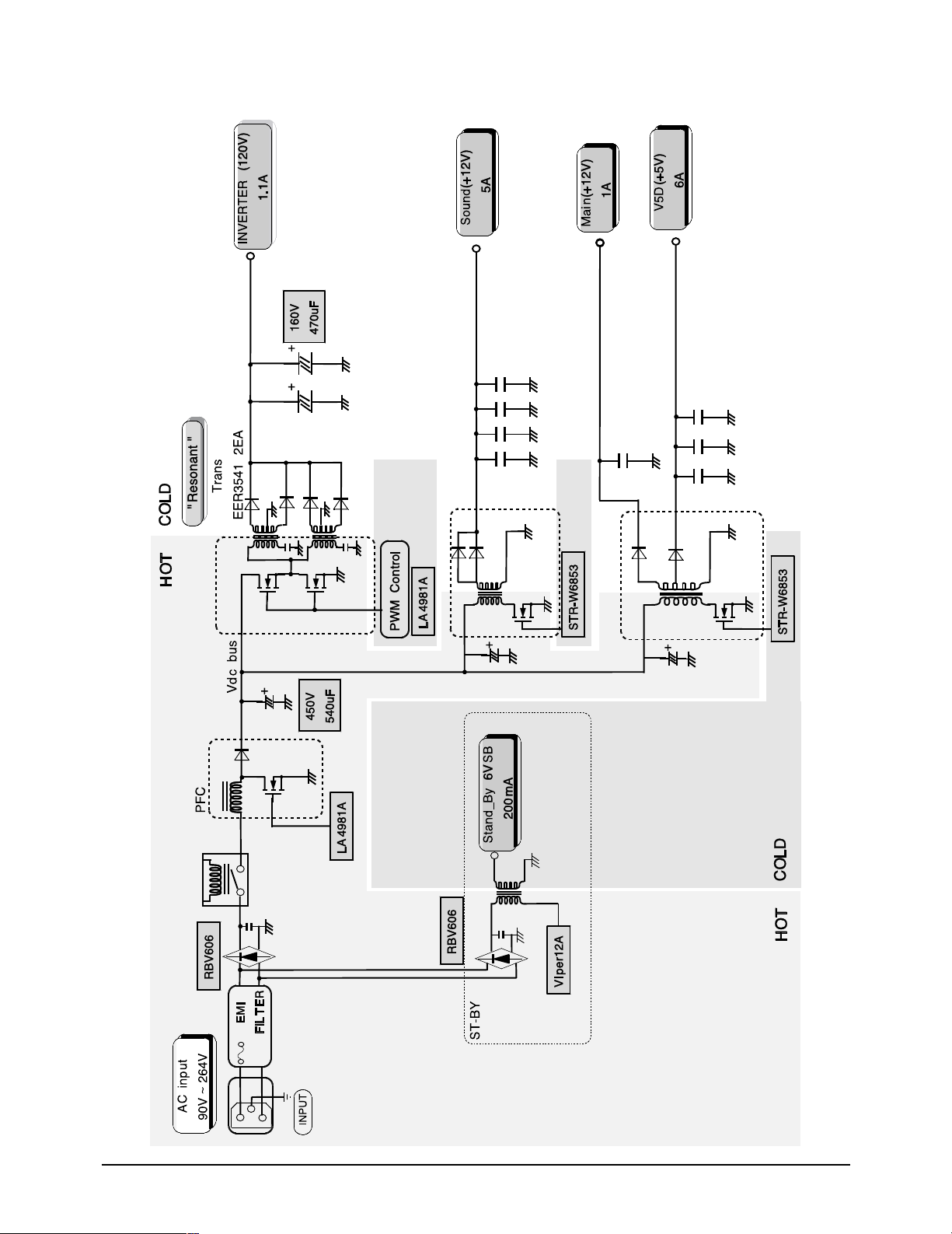
Power Block diagram
Page 6
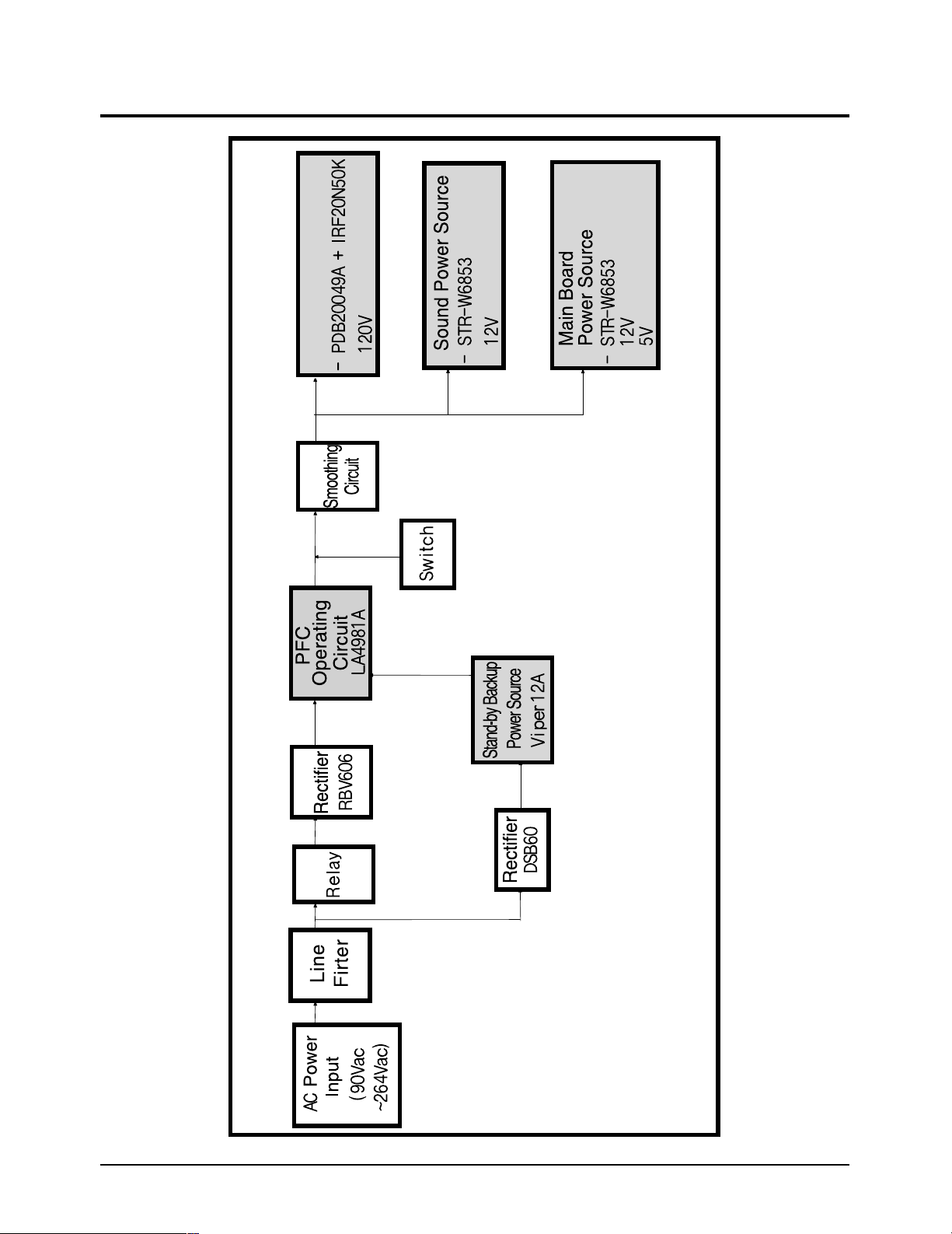
LCD-TV 32”, 40” Power Block diagram
Block Diagrams
LW32A23W/LW40A23W
Inverter Power Source
Page 7
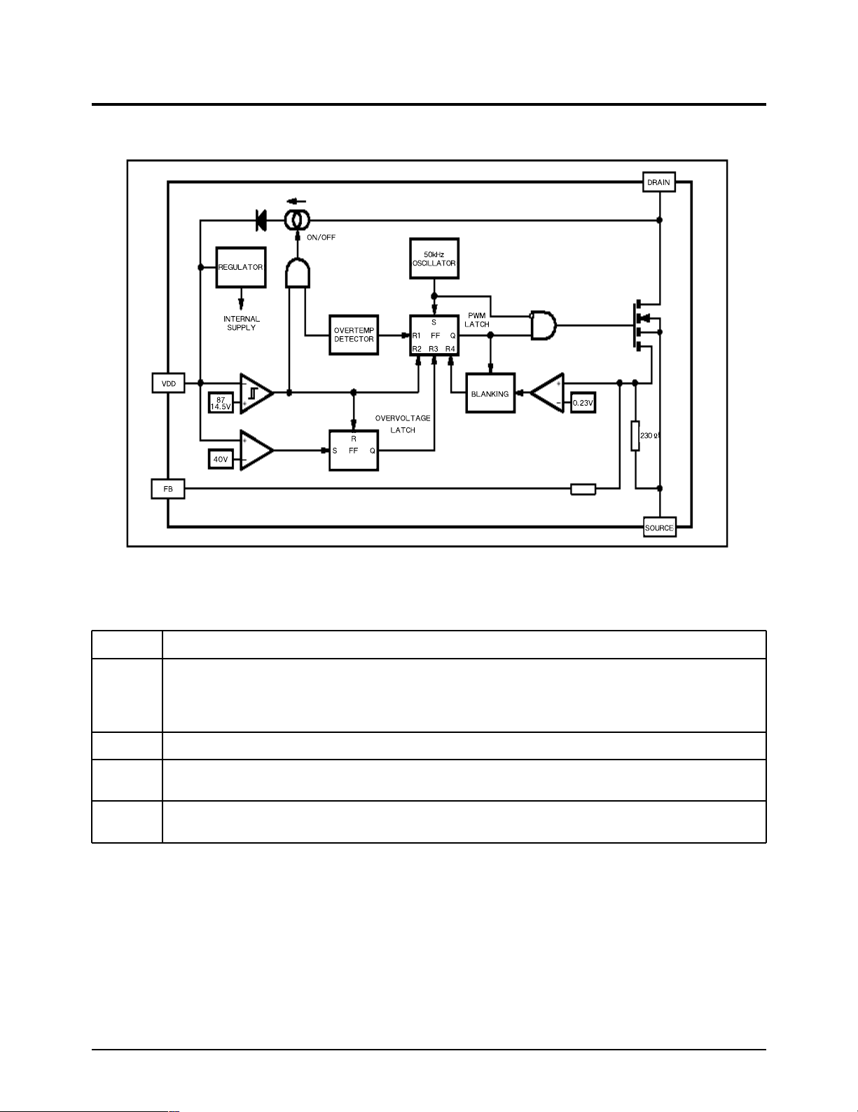
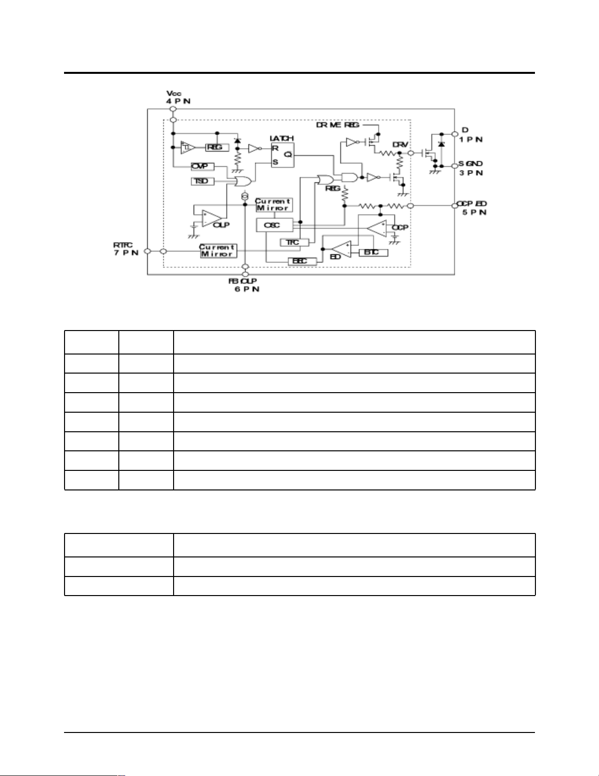
function
For supplying power to the control circuit,dividing the charged current of the high-voltage current source connected to the drain
during startup,and comparing VDD voltage hysteresis.
Divided into two threshold voltages VDDon to start switching and to disconnect the startup current source (normally 14.5V), and
VDDoff to stop switching and to operate the startup current source (normally 8V)
Power MOSFET source and the circuit reference ground (GND)
Power MOSFET drain.Also used during startup as the internal high-voltage current source
until the external VDD capacitor is charged.
Feedback input.Operating voltage range of 0V ~1V.Determined by the maximum MOSFET current value.
The current limit in due consideration of the maximum drain current is included in the FB pin that is connected to the source pin.
Block Diagrams
LW32A23W/LW40A23W
Backup Power Source
Viper 12A Block Diagram
Pin Functions
Name
VDD
SOURCE
DRAIN
FB
Page 8

Block Diagrams
LW32A23W/LW40A23W
PFC Circuit
Operating Principles
As the stand-by power circuit starts oscillating,the control IC of the PFC circuit (L4981) is applied with Vcc
and starts oscillating. The oscillation frequency is determined by the resistance (RP824) connected to 17Pin
and the condenser (CP816) connected to 18Pin. For regulation,the output voltage is divided by resistors and
monitored by 14Pin. The 4Pin voltage, which is entered after dividing this voltage and the AC voltage by
resistors, is calculated in the IC and the command value of the main FET is prepared. Therefore, the output
voltage is controlled by the voltage determined by the dividing resistors, and the input current has the
same waveform (sine wave) as the AC voltage, producing a power factor of almost 100%.
Protections
1. Overvoltage
The circuit has an overvoltage protection function of the voltage limit type. In the event of a sudden
interruption of the input, of overshooting [overload?] during a sudden change of load,or non-control
status, this function protects the circuit by narrowing the ON width of the FET and preventing the
voltage from rising above the overvoltage setting. The overvoltage can be set with RP834, RP835, RP836
and RP840. (The power source is set to approximately 385V)
2. Overcurrent
The current is converted into the voltage value through RP831 and RP832,and monitored by 2 Pin and 8
Pin of the control IC. If the voltage of the detecting resistor rises above the set value due to an increase in
current, the pulse width is narrowed to limit the output.
3. Thermal Shutdown
Although the IC has a thermal shutdown function, a thermistor (TH) is installed on the heat-radiating fin
of the main FET and the circuit is stopped if overheated by overload, etc.
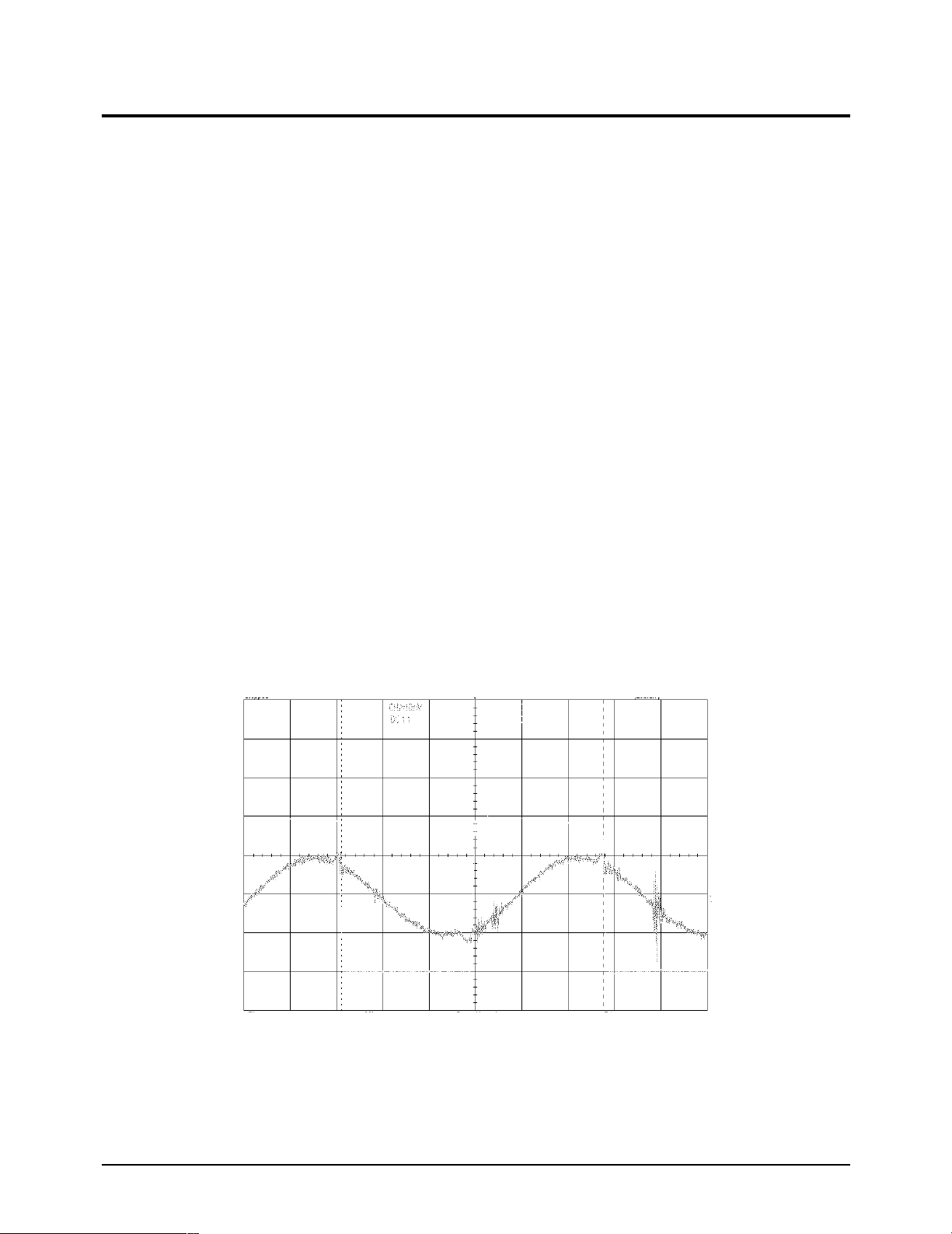
FET VDS Waveform (Input of 100V) FET VDS Waveform (Input of 230V)
Page 9
Block Diagrams
LW32A23W/LW40A23W
Resonance Circuit (Power Source for Inverter)
Operating Principles
Explains the circuit of the power source for the inverter. With the operation of the MULTI block, a voltage is
generated in the ancillary windings (4-5Pin) of T804S and is applied to 1 Pin (Vcc terminal) of the resonance
circuit to start oscillation. High side FET (Q4) and low side FET (Q5) are turned on alternately, delivering
energy to the secondary circuit. For voltage regulation, the output voltage is divided along resistors and
monitored by the transistor (QI809), and the photo coupler (PC801S) is turned on or off. If the output ,
voltage rises, PC801S is turned on and draws current from 13 Pin of the resonance circuit. The switching
frequency then increases, reducing the charge period of the resonance condenser (CI811) and thereby
limiting the output voltage. On the other hand , if the output voltage decreases, no current is drawn from
13 Pin of the resonance circuit and the switching frequency decreases, extending the charge period of the
resonance condenser and thereby raising the output voltage.
Protections
1. Overvoltage
The output voltage is divided along the resistors and monitored by QI810. If the output voltage rises, the
QI810 voltage also rises, which triggers QO810 to turn PC802S on. This will increase the voltage at 5 Pin
of the resonance IC, which stops oscillation in the latch mode.
2. Overcurrent
The current flowing in the resonance condenser (CI811) is divided through CI808, converted into voltage
at the resistors (RI809, RI816) and is monitored by 3 Pin of theresonance IC. If the output current rises,
the current in the primary winding wire also rises, which triggers the voltage at 3 Pin of the IC to rise as
well. If the voltage exceeds the set value, the pulse width is narrowed to limit the current.
3. Thermal Shutdown
The resonance IC has a built-in thermal shutdown function and stops oscillation at over 125 ˚C
FET VDS Waveform of the resonance circuit
Page 10

Block Diagrams
LW32A23W/LW40A23W
Main Board Supply &Sound Exclusive IC of STR-W6853
Outlines
1. A new 7 Pin package has been developed from the existing 5 Pin package. High-power MOSFET is
embedded in a small package to save space.
2. The distance between the pins of MOSFET drain & source has been widened to 1.8mm where high
voltage is applied,allowing the loading of high anti-pressure MOSFET.
3. The operation mode changes in 3 stages according to the load applied, and saves power consumption.
TFC, MBS, and pseudo-oscillation are available.
Features
1. Improvement of power efficiency through automatic conversion of operation modes the controlling MIC
part saves power consumption through a BCD processor. W6800 series changes the operation mode in 3
stages according to the load applied and saves power consumption.
1) Pseudo-oscillation under load
2) If MBS (Multi, Bottom, Skip) frequency exceeds 70 kHz under medium or small loads, the bottom is
skipped while bottom, ON is maintained.
3) If TFC (Time, Fix, Control)operation extends the ON time forcibly under St-By load, the OFF time is
controlled to lower the oscillating frequency. In the event of compulsory ON, control by external
resistors is possible.
2. Major Features
1) Embedded overcurrent protection (OCP) of pulse by pulse
2) Embedded overload protection (OLP) of latch shut down.
3) Embedded thermal shutdown function.
4) Embedded overvoltage protection for input voltage
5) Adjustable frequency for TFC operation
Page 11
Block Diagrams
LW32A23W/LW40A23W
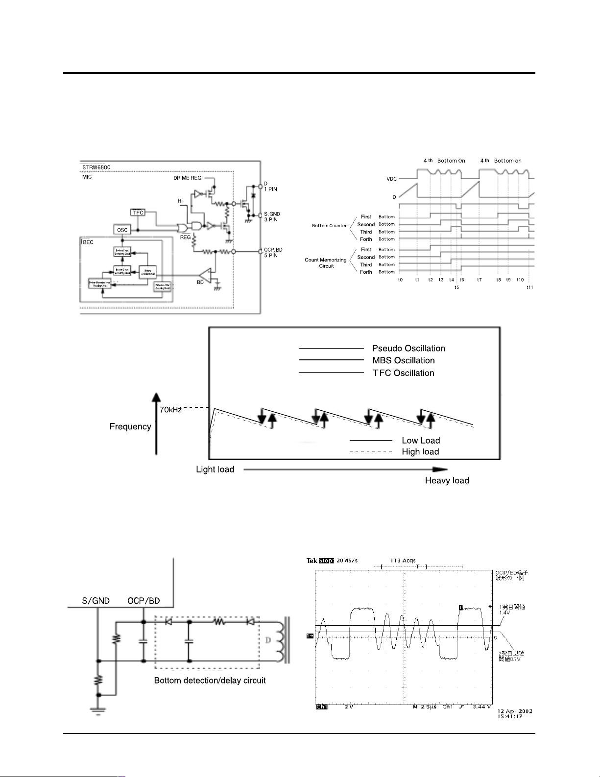
Block Diagram
Terminal Functions
Other Functions
Terminal
Number
Symbol Name and Functions
1
2
3
4
5
6
7
D
NC
S/GND
Vcc
OCD/BD
FB/OLP
RTFC
MOSFET Drain terminal
Not Connect
MOSFET Source / Ground terminal
Control circuit power input terminal
Overcurrent detection signal input terminal / Bottom detection signal input terminal
Voltage control signal input terminal / Overload protection detection terminal
Fixed ON time adjustment terminal
Symbol Functions
TSD
OVP
Thermal Shutdown Circuit
Overvoltage circuit
Page 12
Block Diagrams
LW32A23W/LW40A23W
Operation of W6853
Outlines
1. MBS : Multi bottom skip (medium load area)
The circuit has the PWM reference time T=14uS, 70 kHz internally and is designed to turn on at a bottom
less than 14uS.
Note : MBS operations should not be counted in the overload, overcurrent area. (Bottom is not extended)
If the overload condition continues, OLP will be triggered to shut down the operation. Normally ,it
is not counted during startup, and if the down edge is detected only once after a count of 2, it is
considered abnormal and the oscillation is stopped.
Sub circuit
MIC internal reference time
On at a Bottom after the Reference Time that starts with ON.
On with the Bottom Count same as memorizing circuit.
Circuit
Page 13

Block Diagrams
LW32A23W/LW40A23W
2. TFC : Time fix controller (Lighter load area during stand-by) TFC operation forcibly outputs to DRV an
ON time (T2) that is longer than the fixed Ton (T1) inside the MIC to control the OFF time for stabilizing
the output voltage. If MBS operation under light load moves toward the light load area again, the MBS
operation is released at Ton=350 us and shifted to the TFS operation.
3. OLP
Page 14

Block Diagrams
LW32A23W/LW40A23W
4. Vcc Terminal,Startup Circuit
Startup is performed by the startup resistor and the condenser between Vcc and S/GND.
The startup voltage, Vcc is 18.2V (typ)and starts the circuit by charging C2 from the startup resistor.
After startup, operation continues with power supplied from the transistor drive winding wire .
(Near the drive winding wire and stand-by power source;Startup of Vcc)
Startup resistor
Peck charge
prevention resistor
5. OCP / OLP
From the transistor design, under medium load with only one bottom left,it is possible for Id to exceed
50%of the normal pseudo oscillation duty.In particular,if there is still a bottom under the maximum load at
VinAC (Min), confirming the condition is required. The following is an explanation of the pseudo
oscillation signal input of the OCP/BD terminal.
Page 15

Block Diagrams
LW32A23W/LW40A23W
6. RTFC Terminal
Adjustment should be performed while checking the actual operation in the range of 100k to 1 M.During
an IC examination, you may sometimes find minimum oscillating frequency at the RTFC resistor, but as
the secondary circuit performs feedback control, Id determined by ton at RTFC shows changes in the
peak value due to the primary inductance lp of the transistor and the winding ratio. If the load
consumed by the secondary circuit is constant, the peak value of Id increases and the frequency
decreases as lp becomes smaller and the ton setting becomes larger.
7. Phase Correction
When you have an unusual type of secondary feedback circuit and
load specifications, if the phase correction of the error amp on the
secondary circuit is not sufficient, due to the capacity of the
smoothing input condenser being too small and the ripple voltage
being too high, you can get a good result by adding a condenser
between the FB/OLP terminal of W6800 and S/GND. The FB/OLP
terminal is fitted with latch delay CR.If R is small, it may improve
the shift start during startup,but may also cause extreme delay.
Therefore ,care should be taken to avoid excessive response in
changing the loads.
Page 16

LW32A23W/LW40A23W
SW_SMPS
GND
STD_VCCGA
AGND
CH+_OUT
VOL+_OUT
BUZER_IN
AGND
CH-_OUT
VOL-_OUT
SOURCE_OUT
AGND
STD_VCC3B
VCC5B
AGNDIRLED_GRN
LED_RED
AGND
AV_CVBS
AGND
SVHS_Y
MENU_OUT
AGND
STD_VCC5B
VCC5DDC
AGND
SVHS_C
AGND
SC1_RGB_FB
CN800
GND_AMP
HP_IDENT
GND_AMP
HP_OUT_L
GND_AMP
HP_OUT_R
GND_AMP
WOOFER_OUT
GND_AMP
MAIN_L_OUT1
MAIN_L_OUT2
MAIN_R_OUT1
MAIN_R_OUT2
GND_AMP
SUR_L_OUT1
SUR_L_OUT2
GND_AMP
SUR_R_OUT1
SUR_R_OUT2
GND_AMP
CENTER_OUT1
CENTER_OUT2
GND_AMP
GND_AMP
CN510
VCC5I
VCC5P
VCC5P
VCC5P
VCC5P
GND_PANEL
GND_PANEL
GND_PANEL
PANEL_Y_DEC
PANEL_Y_INC
SW_ACCE
GND_PANEL
TXOUT 3+
TXOUT 3-
GND_PANEL
TXCLKOUT+
TXCLKOUT-
GND_PANEL
TXOUT 2+
TXOUT 2-
VCC12A
GND
VCC5A
VCC5A
VCC5A
GND
GND
GND
VCC12BS
VCC12BS
VCC12BS
GND_AMP
GND_AMP
GND_AMP
GND_PANEL
TXOUT 1+
TXOUT 1-
GND_PANEL
TXOUT 0+
TXOUT 0-
GND_PANEL
SW_INVERTER
ANA_DIMMING
PWM_DIMMING
CN505
SC1_R_SC1_SVHS_CI
SC1_G
SC1_B_SC1_SVHS_C0
AGND
SC1_CVBS_IN
AGND
SC1_CVBS_OUT
AGND
SC2_CVBS_IN
AGND
SC2_SVHS_CI
AGND
Y_D1
AGND
PB_D1
PR_D1
AGND
Y_D2
AGND
PB_D2
PR_D2
AGND
AGND
SC2_CVBS_OUT
ANGD
SC2_SVHS_CO
Y_COMP1
AGND
PB_COMP1
PR_COMP1
CN506
Y_COMP2
AGND
PB_COMP2
PR_COMP2
D4_1_CON1
D4_1_CONT2(SC1_S)
D4_1_CONT3
D4_2_CONT1
D4_2_CONT2(SC2_S)
D4_2_CONT3
AV_L
AGND
SC1_L_OUT
SC1_R_OUT
AGND
SC2_L_IN
SC2_R_IN
AGND
SC2_L_OUT
SC2_R_OUT
AGND
COMP1_L
AV_R
GND
SC1_L_IN
SC1_R_IN
COMP1_R
AGND
COMP2_L
COMP2_R
CN509
PC_L
PC_R
AGND
COAXIAL_IN
AGND
OPTICAL_IN
AGND
PC_RED
PC_GREEN
PC_BLUE
AGND
DDC_DVI_SDAS
IDENT_PC
RX0-
RX0+
DGND
RX1-
RX1+
DGND
RX2-
RX2+
DGND
PC_DDC_HSYNC
PC_DDC_VSYNC
AGND
DDC_DVI_SCLS
RXC-
RXC+
DGND
DDC_VCC5D
CN507 CN508
Wiring Diagram
Page 17

LW32A23W/LW40A23W
AGND
AGND AGND
GND
OUT8
VCCOUT1
OUT2
OUT3
OUT4
OUT7
OUT6
OUT5
IN6
VCCP
IN1
SDA
IN2
GND
OUT8
VCC
OUT1
OUT2
OUT3
OUT4
OUT7
OUT6
OUT5
IN6
VCCP
IN1
SDA
IN2
SCL
IN3
IN5
SUB
IN4
COMP_9883_PR
COMP_9883_PB
COMP_99883_Y
COMP_9883_PB
COMP_99883_Y
COMP_9883_PR
PRY
PB
SCL1
SDA1
3230_DCLK
OUT1
OUT2
OUT3
OUT4
OUT7
OUT6
OUT5
IN6
VCCP
IN1
SDA
IN2
SCL
IN3
IN5
SUB
IN4
GND
OUT8
VCC
PIN
PIN
PIN
PIN
PIN
23
66
94
110
140
3.3V
PIN
PIN
PIN
SCL
IN3
IN5
SUB
IN4
9883A_VSYNC
9883A_HSYNC
9883A_COAST
SC2_CVBS_IN
SC1_CVBS_IN
DPTV_CVBS
3230C(0:7)
3230Y(0:7)
3230C(0:7)
3230Y(0:7)
3230C(0:7)
3230C(0:7)
OPTION
10uF
3230Y(0:7)
DPTV_SVHS_C
DPTV_SVHS_C
DPTV_CVBS
DPTV_CVBS
DPTV_SVHS_Y
DPTV_SVHS_Y
3230_SVHS_C
3230_SVHS_Y
3230_VS
3230_HS
3230_VS
3230_HS
DPTV_CR
DPTV_Y
DPTV_CB
V_SYNC
H_SYNC
PIN
PIN
52
80
125
156
174
2.5V
10uF
C740
C738
10uF
C736
10uF
10uF
C737
C735
C733
10uF
MO
1/16W
10K
R9484
R9483
16V
100nF
C8304
R9482
75
R9481
75
R9471
75
R9475
180
4.7K
1/16W
1/16W
1K
B
Q907
E
C
B
KSA1182
GND_9883
R9474
VCC3D_DPTV
FT940
C
3
2
1
A
LFB30-3A1E223M
75
75
R279
C2187
220nFC2181
10pF
R281
R2827575
C2185
10pF
R280
10pF
C2184
220nF
10pF
C2183
220nF
C2180
R271
C2182
R9451
75
R288
75
75
R286
7575R275
75R276
3
21
D718
D715
3
21
D717
D714
3
21
D716
1
MMBD4148SE
D713
3
21
MMBD4148SE
3
21
MMBD4148SE
D712
3
2
3
21
MMBD4148SE
D711
3
21
MMBD4148SE
D710
3
21
MMBD4148SE
R9450
100
1/16W
R284
5.1K
5.1K
R283
R265
22
4.7K
22
R237
R239
VCC5C
C2167
R238
22
100nF
3.3K
R260
470
C2170
10uF
16V
R261
50V
1uF
C2169
3.3K
R263
R264
470
3.3K
FT210
3
R258
R259
470
C2168
C
B
2
1
A
LFB30-3A1E223M
R262
IC205
100nF
GS1881-CKA
680K
1.5nF
8
7
6
5
4
3
2
1
C229
C204
C233
1.5nF
1.5nF
1.5nF
C220
C224
1.5nF
1
T230
C253
100nF
RA204
8765432
1
3
2
1
SUPLECODE
SUPLECODE
RA205
876
87654
432
1
SUPLECODE
RA206
RA207
87654352
1
SUPLECODE
L200
B
2
3.3UH
FT205
3
C
B
21
A
LFB30-3A1E223M
FT206
3
C
220nF
A
1
LFB30-3A1E223M
100nF
C741
R255
C722
220nF
10K
C721
10
100
R746
R207
100R745
20K
R743
1/16W
10K
R744
R741
R742 4.7K
4.7K
4.7K
R739
R740
4.7K
4.7KR737
VCC8B
R738 4.7K
LFB30-3A1E223M
C
3
2
B
A
1
FT712
16V
47uF
C732
C739
C742
220nF
TEA6425D
100nF
19
S
R
18
Q
17
P
16
O
15
14
N
12
L
11
K10J
9
I
8
H
7
G
6
20
T
R726
F
5
E
4
D
3
C
2
B
1
A
IC702
VCC3A_DPTV
13
M
7
6
4.7K
1
RA209
88
7
6
5
4
35
4
3
2
1
RA208
8765432
1
RA211
2
8
100nF
765
432
1
RA210
C265
100nF
C261
100nF
C263C262 C264
100nF
C2160
1uF
50V
100nF
C2157
1uF
50V
50V
1uF
C2156
3.3UH
L201
47R253
R254
16V
100uF
22
22
16V
100uF
R256
10nF
C2149
33pF
C2152
100nF
C2148
C2138C2133
C2144
C2139
C2143
100nF
33pF
C2137
33pF33pF
100nF100nF
C2136C2135
C2142
100nF
C2141
33pF33pF
100nF
C2134
C2145
100nF
100nF
C2140
C2151
C2162
100nF
100nF
C2153
C2165
C2154
100nF
16V
100nF
C2132
100
C2163
100nF
R251
100
100uF
R252
1nF
C2155
C2161
100nF
C2159
100nF
100nF
C2158
R250
10K
C2146
R248
3.3K
39nF
C2147
10K
3.9nF
100nF
C2150
R249
23
22
VDD2
11
100nF
C2164
VD10
62
26
VD1
65
MST9883A-110
31
VSYNC
64
VSOUT
VDD6
79
78
VDD5
69
VDD4
VDD3
74
RED3
75
RED2
VDD1
59
VD9
52
VD851VD746VD6
VD5
45
42
VD4
39
VD3
27
VD2
2
3
GREEN6
4
SOGOUT
49
SOGIN57SDA56SCL58REF_BYPASS
70
RED7
71
RED6
72
RED5
RED4
73
GND6
25
24
GND5
21
76
RED1
77
RED0
54
RAIN
35
PVD2
34
PVD1
MIDSCV
37
30
HSYNC
66
HSOUT
GREEN7
50
GND1447GND13
GREEN55GREEN46GREEN37GREEN28GREEN1
GREEN0
9
36
GND9
32
GND8
28
GND7
CLAMP
38
12
BLUE7
GND4
20
GND3
80
GND20
10
GND2
68
GND19
63
GND18
61
GND17
60
GND16
GND15
53
BLUE317BLUE2
BLUE1
18
44
GND1241GND11
40
GND10
1
GND1
48
GAIN
FILT
33
67
DATACK
29
COAST
A0
IC202
R708
4.7K
13
BLUE614BLUE515BLUE4
16
16V
10uF
19
BLUE0
43
BAIN
55
C709
R725 4.7K
4.7KR724
4.7KR723
R722 4.7K
16V
10uF
C720
C717
10uF
16V
16V
10uF
C716
C715
10uF
16V
16V
10uF
C719
C718
10uF
16V
4.7KR721
R719
R720 100
100
2
B
A
1
FT711
VCC8B
C723
47uF
16V
N
IC701
C
3
T
20
S
19
18
R
17
Q
16
P
15
O
14
M
13
L
12
K11J
10
I
9
H
8
G
7
C205_OP
F
6
E
5
D
4
C
3
B
2
A
1
TEA6425D
10pF
1/16W
100
10pF
R202
R201
C206_OP
R220
100
100
1/16W
R701
R700
47
100
C240
33pF33pF
C239C238
33pF
33pF
C256 C260
33pF33pF
C259C257
C231
33pF
100
33pF
C258
R236
R235
100nF
100
75
R230
R229
75
75
R228
R227
75
75
R226
R225
75
3
C
B
2
1
A
C2120
10uF
16V
3
C
B
2
A
1
C235
FT201
16V
FT200
100nF
1
SUPLECODE
RA202
8
C234
10uF
876
57
65432
1
SUPLECODE
RA203
8
7
6
5
4
3
2
432
1
RA201
SUPLECODE
SUPLECODE
C207
8
7
6
5
4
3
2
1
RA200
680NF
4.7K
680NF
C214
R706
4.7K
R705
R715
R707
4.7K
R716
R714
22
22
22K
R710
22K
12K
22uF
R711
12K
R709
16V
16V
47uF
C711
C710
22uF
16V
VCC5C
75
C700
R718
Q701
3
C
B
2
1
A
FT710
E
C
B
2SC2412K-Q
C712
100pF
1K
R717
R702
4.7K
C706
10uF
16V
2SC2412K-Q
VCC5C
R712
Q700
VCC8B
75
C705
C704
10uF
16V
E
C
B
16V
10uF
16V
10uF
C703
C702
10uF
16V
R704
4.7K
TEA6425D
20
T
19
S
16V
10uF
C701
O
15
14
N
13
M
12
L
11
K
H
7
G
6
F
5
E
4
D
3
CR
18
Q
17
P
16
IC700
100pF
10
J
9
I
8
C714
R713
2
B
1
A
1K
4.7K
R703
C754
220nF
220nF
C707
22
R200
C226
0.39nF
C223
47nF
C227
10uF
16V
220nF
680NF
C222
C225
C221
220nF
C219
0.39nF
47nF
C217
C210
16V
10uF
C218
4.7pF
C213
10uF
16V
C211
VCC5C
C203
47nF
4.7pF
68nF
C202
C200
68nF
VCC3D_DPTV
68nF
C201
R206
47nF
C232
R204
0.39nF
C228
100
R205
C230
100
220nF
100
IC201
18
YCOEQ
31
Y7
Y633Y5
Y4
34
37
Y3
Y2
38
39
Y1
Y0
40
XTAL2
63 62
XTAL1
VSUPY
36
52
VSUPSY
26
29
VSUPLLC
69
VSUPF
10
VSUPD
9
VSUPCAP
VSUPC
45
VSUPAI
76
VSTBY
59
VS
57
VRT
66
VREF
32
27
LLC2
LLC1
78
VOUT
70
75
VIN4
VIN3
74
73
VIN2
VIN1
72
17
VGAV
16
TEST
14
SDA
13
VSUPPA
GNDPA
GNDLLC
30
65
GNDF
11
GNDD
12
SCL
15
RESQ
6
R2
3
R1
NC_2
61
8
NC_1
56
MSY
G2
2
G1
FSY
5558
FPDAT
20
FFWE
28
ISGND
68
INTLC
53
67
I2CSEL
35
GNDY
GNDSY
51
25
B2
21
FFRSTW
22
FFRE
23
FFOE
19
FFIE
79
FB1IN
60
CLK5
24
CLK20
GNDCAP
46
GNDC
77
GNDAI
5
71
CIN
C7
4142
C6
C5
4344
C4
C3
4748
C2
C1
4950
C0
41
B1
54
AVO
64
ASGF_2
7
ASGF_1
AISGND
80
VPC3230D-C5
HC-49/SM5H(20.25MHz)
Q1
Q0
X201
1
C212
100nF
10K
1
T204
R224
T203
1
T202
T201
C286
22uF
1
16V
100nF
VCC3D_DPTV
C280
C281
100nF
100nF
C284
C282
C283
100nF100nF
100nF
C
3
2
B
A
1
FT207
C285
100nF
100nF
C275
C274
C276
100nF
100nF
C277
R247
C278
100nF
100nF
C279
K4S643232E-TC60
33
84
VSSQ8
78
VSSQ7
VSSQ6
52
46
VSSQ5
VSSQ4
38
32
VSSQ3
12
VSSQ2
VSSQ1
6
86
VSS4
VSS3
72
58
VSS1
44
81
VDDQ8
75
VDDQ7
VDDQ6
55
49
VDDQ5
VDDQ4
41
35
VDDQ3
VDDQ2
9
3
VDDQ1
VDD4
17
WE_
DQM1
71
DQ9
76
43
29
VDD3
VDD2
15
VDD1
1
RAS_
19
N_C7
73
N_C6
70
N_C5
69
N_C4
VSS2
7
DQ3
53
DQ29
DQ28
51
50
DQ27
57
N_C3
30
N_C2
21
14
N_C1
16
DQMO
DQM3
5928
DQM2
37
DQ2
5
36
DQ19
DQ18
34
33
DQ8
7413
DQ7
11
DQ6
10
DQ5
DQ4
8
DQ31
56
DQ30
54
DQ10
77
DQ1
4
DQ0
2
CS_
20
48
DQ26
DQ25
47
DQ24
45
DQ23
42
DQ22
40
DQ21
39
DQ20
A7
64
63
A6
62
A5
61
A4
DQ17
31
DQ16
DQ15
85
83
DQ14
82
DQ13
80
DQ12
79
DQ11
22uF
16V
68
CLK
67
CKE
18
CAS_
BA1
23
BA0
22
66
A9
65
A8
C273
60
A3A2
27
A10
24
A1
26
A0
25
IC204
C271
100nF
C270
100nF
C269C268
100nF100nF 100nF100nF
C267C266
17
WE_
84
VSSQ8
78
VSSQ7
VSSQ6
52
46
VSSQ5
VSSQ2
VSSQ1
6
86
VSS4
VSS3
72
VSS2
58
44
VSS1
81
VDDQ8
VDDQ7
75
K4S643232E-TC60
35
VDDQ3
VDDQ2
9
3
VDDQ1
43
VDD4
29
VDD3
VDD2
15
VDD1
1
RAS_
19
VSSQ4
38
32
VSSQ3
12
10
DQ5
DQ4
8
N_C7
73
N_C6
70
N_C5
69
N_C4
5730
N_C3
N_C2
21
VDDQ6
55
49
VDDQ5
VDDQ4
41
DQ24
42
DQ23
DQ22
14
N_C1
DQMO
16
DQM3
5928
DQM2
71
DQM1
DQ9
76
74
DQ8
13
DQ7
11
DQ6
83
DQ14
82
DQ13
56
DQ31
DQ30
54
DQ3
7
DQ29
53
DQ28
51
50
DQ27
DQ26
48
47
DQ25
45
23
BA1
BA0
22
40
DQ21
39
DQ20
37
DQ2
5
36
DQ19
34
DQ18
33
DQ17
DQ16
31
DQ15
85
24
A1
26
25
80
DQ12
79
DQ11
DQ10
77
DQ1
4
2
DQ0
CS_
20
CLK
68
CKE
67
18
CAS_
A9
66
65
A8
64
A7
63
A6
62
A5
61
A4
60
A3A2
27
A10
100nF
A0
IC203
VCC3D_DPTV
3
C
B
2
A
1
FT204
R215 100
C272
100
1
T200
R214
3.3UHL204
47pF
C2126
47pF
C2125
C2129
47uF
16V
33pF
C2118
33pF
1/16W
4.7K
33pF
C237
C236
R223
C251
R241
22
100nF
VCC3A_DPTV
LFB30-3A1E223M
22
C
3
2
B
A
1
FT203
R240
16V
47uF
C
3
2
BA
1
FT202
C2166
47uF
16V
R245
C241
3333R246
R244
16V
22uF
33
C296
C2119
100nF
R221 100
C250 100nF
16V
22uF
C2116
16V
22uF
C2105
C297
22uF
16V
3.3UH
3.3UHL202
L207
3.3UH
100nF
L205
C287
C2117
100nF100nF
HC-49/S-SMD(14.31818MHZ)
Q1
Q0
X200
3.3UH
C288
L208
C289
22uF
16V
VCC2.5D_DPTV
C292
3.3UH
L209
16V
1nF
C290
22uF
C291
16V
100uF
C2123
100nF
1nF
C2124
C2101
22uF
16V
22uF
C2110
C299
22uF
16V
C29522uF 16V
16V
100pF
C249
C2115
100nF
VCC5C
1uF
C252
22uF
1uF
C2113
C2112
C2114
22uF
C2109
100nF
C2108
100uF
3.3UH
L206
100nF
C2111
C2107
100pF
C2106
100nF
100nF
100nF
C2103
100nF
C2104
VCC3A_DPTV
C2102
L203
VCC2.5D_DPTV
R210
10K
3.3UH
C2100
100nF
100nF
C298
100nF
C255
100
R234
R218
22
100
R290
100
C293
R233
20pF
20pF
VCC3D_DPTV
VCC2.5D_DPTV
C294
C242
100nF
100nF
C243
C244
100nF
C245
100nF
33
C247
R243
C246
C248
100nF
100nF
100nF
R231
33
75
R232
R242
VSYNC
35
VSS9
155
VSS8
141
126
DPTV-3D-6830-C
390
VSS10
173
24
VSS1
VPROT
37
26
VM
VLF
XTLO
164
XTLI
163
WR
176
WE
101
40
VSYNCPIP
43
VSYNCMP
140
VDD5
110
VDD4
94
VDD3
66
VDD2
VSS7
VSS6
111
95
VSS5
VSS4
81
67
VSS3
VSS2
53
193
VSS11
RT2
RT1
202
RESET
5
RD
177
RB2
204
161
192
VDD_ADC
174
VDDC5
156
VDDC4
VDDC3
125
80
VDDC2
52
VDDC1
MD9
MD8
79
82
MD7
154
MD63
MD62
153
152
VDD1
23
V5SF
1
2
TEST
SD
178
SC
179
203
147
146
MD55
MD54
145
144
MD53
MD52
143
142
201
RB1
99
RAS
R
27
6
PS
MLF
158
78
MD46
135
134
MD45
MD44
133
132
MD43
MD42
131
MD61
151
MD60
MD6
83
150
MD59
MD58
149
148
MD57
MD56
MD37
MD36
123
122
MD35
MD34
121
120
MD33
MD32
MD51
139
MD50
84
MD5
138
MD49
137
MD48
136
MD47
MD27
MD26
59
60
MD25
MD24
61
62
MD23
MD22
130
MD41
MD40
129
MD4
85
128
MD39
127
MD38
124
70
MD17
MD16
71
72
MD15
MD14
73
74
MD13
119
54
MD31
MD30
55
86
MD3
56
MD29
MD28
57
58
MCLK
MA9
113
112
MA8
MA7
109
108
MA6
MA5
63
MD21
64
MD20
65
MD2
87
MD19
68
MD18
69
31
INT2
3
180
INT
HSYNCPIP
39
HSYNCMP
42
34
MD12
75
76
MD11
MD10
77
88
MD1
89
MD0
96
DQM4
115
DQM3
93
92
DQM2
DQM1
91
90
DQM0
107
MA4
106
MA3
105
104
MA2
MA1
103
102
MA0
IRSET
185
CVBS3
CVBS2
184
183
CVBS1
98
CS1
CS0
HSYNC
36
HFLB
28
G
118
DQM7
117
DQM6
116
DQM5
CLKPIP
41
CLKMP
CCLP3
208
198
CCLP2
187
CCLP1
207
CB
100
CAS
CAPD9
21
CVBS_OUT2
189
188
CVBS_OUT1
CVBS4
186
CAPD6
45
46
CAPD5
CAPD4
47
48
CAPD3
CAPD23
7
8
CAPD22
CAPD21
9
10
CAPD20
CAPD2
49
97
197
CR
38
CAPD18
CAPD17
13
14
CAPD16
CAPD1515CAPD1416CAPD13
17
18
CAPD12
CAPD11
19
20
CAPD10
50
22
CAPD8
44
CAPD7
C
196
114
BA
B
29
AVSS_1
25
AVSSA5
206
200
AVSSA4
195
AVSSA3
191
AVSSA2
AVSSA1
182
CAPD19
11
12
AVSS2
AVSS1
159
AVSS
30
AVDDA5
205
199
AVDDA4
AVDDA3
194
AVDDA2
190
AVDDA1
181
162
AVDD2
AVDD1
CAPD1
CAPD0
51
175
ALE
4
ADDRSEL
AD7
165
166
AD6
AD5
167
168
AD4
AD3
169
170
AD2
AD1
AVSS3
33
160
PPMM_VS_PIP
PPMM_HS_PIP
PPMM_DFCLK
AGND
AGND
AGND
DG_DPTV GND_9883
DG_DPTVGND_3230 AG_DPTVAGND
AG_DPTV
GND_9883
171
172
AD0
IC200
SC1_RGB_FB
GND_3230
SC1_G
SC1_B_SC1_SVHS_CO
SC1_R_SC1_SVHS_CI
157
32
AVDD
3230C(1)
COMP1_PB
COMP1_Y
COMP_PPMM_Y
COMP_PPMM_PB
AGND
COMP2_PR
COMP2_PB
COMP2_Y
COMP1_PR
CSYNC_DTV
SCL3
SDA3
AGND
AGND
AGND
AGND
GND_DPTV
GND_9883
AGND
AGND
AGND
AGND
3230Y(5)
3230Y(4)
3230C(3)
3230Y(3)
3230Y(2)
3230Y(1)
3230Y(0)
3230C(6)
3230C(7)
GND_9883
GND_9883
3230C(2)
3230C(3)
3230C(4)
3230C(5)
COMP_PPMM_PR
AGND
3230C(0)
SC2_SVHS_CI
GND_9883
GND_9883
GND_9883
GND_9883
GND_9883
GND_9883
DG_DPTV
GND_9883
3230C(6)
3230C(5)
3230C(4)
3230C(2)
3230C(1)
3230C(0)
3230C(7)
3230Y(7)
3230Y(6)
3230C(7)
3230C(5)
3230C(3)
AGND
3230_DCLK
SCL3
SDA3
DG_DPTVDGND
GND_3230
AGND
AGND
SC1_R_SC1_SVHS_CI
SVHS_C
SVHS_Y
GND_9883
SCL2
SDA2
CVBS_OUT
AG_DPTV
GND_3230
DPTV_FLD
DG_DPTV
GND_3230
3230Y(7)
AG_DPTV
DG_DPTVDG_PPMMDG_DPTV
3230C(6)
3230C(4)
DG_DPTV GND_DPTV
AG_DPTV
3230C(2)
3230C(1)
3230C(0)
GND_3230
DPTV_DCLK
GND_3230
GND_3230
GND_3230
GND_3230
GND_3230
GND_3230
GND_3230
GND_3230
SC1_CVBS_OUT
AGND
AGND
PIP_CVBS
SC1_CVBS_IN
TUNER_CVBS
SCL3
SDA3
AGND
SC2_CVBS_OUT
SC2_CVBS_IN
AV_CVBS
AGND
DPTV_DE
AGND
AGND
DG_DPTV
AG_DPTV
DG_DPTV
AG_DPTV
DG_DPTV
DG_DPTV
DG_DPTV
DG_DPTV
DG_DPTV
DG_DPTV
DG_DPTV
SCL1
SDA1
DG_DPTV
DG_DPTVGND_DPTV
DG_DPTV
DG_DPTV
DG_DPTV
GND_DPTV
GND_3230
RST_3230
3230Y(4)
AG_DPTV
GND_DPTV
AG_DPTV
AG_DPTV
AG_DPTV
DPTV#31
DG_DPTV
AG_DPTV
DG_DPTV
AG_DPTV
DG_DPTV
DG_DPTV
DG_DPTV
DG_DPTV
DG_DPTV
DG_DPTV
DG_DPTV
DG_DPTV
RST_DPTV
DPTV_VS
DPTV_HS
AG_DPTV
MD(62)
MD(61)
MD(60)
MD(59)
3230Y(1)
3230Y(2)
3230Y(3)
3230Y(7)
3230Y(4)
3230Y(5)
3230Y(6)
3230Y(0)
3230Y(3)
3230Y(2)
3230Y(1)
3230Y(0)
GND_DPTV
AG_DPTV
3230Y(6)
3230Y(5)
MA(1)
MA(0)
MA(8)
MA(9)
MD(45)
MD(44)
MD(43)
MD(42)
MD(41)
MD(40)
MD(58)
MD(57)
MD(56)
MD(47)
MD(46)
MD(63)
MD(26)
MD(27)
MD(28)
MD(29)
MD(30)
MD(24)
MA(2)
MA(1)
MA(0)
MA(8)
MD(15)
MD(25)
MA(7)
MA(6)
MA(5)
MA(4)
MA(3)
MA(2)
DQMA(2)
DQMA(3)
MD(7)
MD(6)
MD(5)
MD(4)
MD(13)
MD(14)
MD(8)
DQMA(0)
DQMA(1)
MD(31)
MD(9)
MD(10)
MD(11)
MD(12)
MD(22)
MD(23)
MD(31)
MD(30)
MD(29)
MD(28)
MD(17)
MD(18)
MD(19)
MD(20)
MD(21)
MD(3)
MD(2)
MD(1)
MD(0)
MD(16)
MA(0)
MA(7)
MA(5)
MA(4)
MA(3)
MA(2)
MA(1)
MD(0:63)
MA(6)
MA(9)
MA(8)
MD(32)
MD(0:63)
MD(35)
MD(34)
MD(33)
DQMA(7)
DQMA(6)
DQMA(5)
DQMA(4)
MD(41)
MD(40)
MD(39)
MD(38)
MD(37)
MD(36)
MD(48)
MD(47)
MD(46)
MD(45)
MD(44)
MD(43)
MD(42)
MD(54)
MD(53)
MD(52)
MD(51)
MD(50)
MD(49)
MD(60)
MD(59)
MD(58)
MD(57)
MD(56)
MD(55)
DPTV_D_C
MD(63)
MD(62)
MD(61)
PAR(6)
PAR(1)
PAR(2)
PAR(3)
PAR(0)
DPTV_D_Y
PAR(7)
PAR(4)
PAR(5)
PAG(4)
PAG(5)
PAG(0)
PAG(1)
PAG(2)
MD(33)
MD(32)
PAG(6)
PAG(7)
PAG(3)
MD(39)
MD(38)
MD(37)
MD(36)
MD(35)
MD(34)
MD(52)
MD(51)
MD(50)
MD(49)
MD(48)
DQMA(0:3)
MD(55)
MD(54)
MD(53)
DQMA(5)
DQMA(3)
DQMA(2)
DQMA(1)
DQMA(7)
DQMA(6)
DQMA(4)
MA(7)
MA(6)
MA(5)
MA(4)
MA(3)
DQMA(0)
MD(4)
MD(3)
MD(2)
MD(1)
MD(0)
MA(9)
MD(11)
MD(10)
MD(9)
MD(8)
MD(7)
MD(6)
MD(5)
MD(17)
MD(16)
MD(15)
MD(14)
MD(13)
MD(12)
MD(23)
MD(22)
MD(21)
MD(20)
MD(19)
MD(18)
MD(27)
MD(26)
MD(25)
MD(24)
6
7
15
23
24
4
25
5
19
20
22
21
Schematic Diagrams
❈ This Document can not be used without Samsung’s authorization.
DPTV, VPC3230, MST 9883 Block Schematic Diagram
Page 18

Schematic Diagrams
4
CVBS Signal
20
IC202,#64,H-Sync Output Signal21IC202,#56 Communichion Data Signal22IC202,#57 Communichion Clock Signal23IC202,#30 H-Sync intput Signal24IC202,#31 V-Sync Intput Signal25IC202,#71~78, 2~10 Data Puls Signal
5
IC200,#3 Clock Signal
6
IC200,#178 Communichion Data Signal7IC200,#179 Communichion Clock Signal
19
IC202,#66,H-Sync Output Signal
15
S-Video signal,CN505,#26(Y),28(C),
IC701,#18(Y),19(C)
Page 19

DVI INTERFACE
R9240_M,R9241_M,R9242_M,R9243_M
FT916_M,FT918_M
Y_D2
Y_COMP2
PR_COMP2
R313_SIL161B
(VCC_14V)
EO MTTX OPTION
C8130_M,C8131_M,C8132_M,C8133_M,C8150_M,C8152_M
B TYPE (RECIEV)
OR SIL169
R316_SIL169
PB_COMP2
NO USE IN ASIA,USA
R305_SIL169
PR_D1
PB_D1
DDC_DVI_SCLS
DDC_DVI_SDAS
DDC_DVI_SCLS
DDC_DVI_SDAS
32bit
RF Input
PB_COMP1
PB_D2
Y_COMP1
PR_D2
PR_COMP1
RF Ant
Y_D1
DVI
Q906_M,Q907_M,Q908_M
DELETE THE PARTS IN BOX.
R304_SIL169
D805
BAT54A
12
3
R141
33K
7
6
D2
D2_1
5
2
G1
4
G2
S1
1
S2
3
20
21
GND3
GND4
22
SI9933ADY-T1
IC804
8
D1
D1_1
D
4
E
5
F
6
G
7
H
8
9
I
J
10
19
GND1
GND2
L
12
M
13
N
14
O
15
P
16
Q
17
18
R
C
3
VO2
4
CN126
SUPLVAL
A
1
B
2
K
11
GND_1
3
6
GND_2
5
N_F
2
VCC
VO1
1
100nF
C886
VCC5I
IC815
BA33B00FP
B
3
C
L913
1.5uH
STD_VCC6A
FT830
1
A
2
C320
100nF
T131
1
R816
10
T105
1
C801
100nF
1
A
2
B
3
C
1uF
C8122C8121
FT831
16V
100uF
C800
1uF
100uF
C881
100uF
16V
1
T259
1
C8127
R9472
4.7K
1/16W
T265
2N7002L
Q909
D
G
S
T106
1
T107
1
KSC1623-Y
Q100
B
C
E
220pF
C107
47nF
C108
L801
0.12nF
C846
16V
100uF
C326
100nF
C824
100nF
C823
1
T260
1
2N7002L
Q908
D
G
S
T261
33K
C119
1uF
T271
1
R140
C109
2.2nF
R101
22K
L802
N
R823
13K
1/10W
1
23
4
C8128
47uF
16V
1
23
4
L917
INSTPAR
T119
1
L916
INSTPAR
1
2
3
4
5
6
7
8
C179
100nF
4
5
6
7
8
RA310
22
22
1
2
3
ACM2012-361-2P
FT304
I1
1
I22O1
3
O2
4
RA311
ACM2012-361-2P
FT303
I1
1
I22O1
3
O2
4
R8304
1/16W
6.2K
R8303
1/16W
12K
R136
33K
FT100
A
1
B
2
C
3
1
100nF
C827
56K
T274
33K
R9357
1
T122
1
R142
MO
25V
39nF
C8188
T121
C170
D111
12
3
100nF
T264
1
1
A
2
B
3
C
680uH
L111
T272
1
VCC2.5T
FT101
2K
1/16W
R319
VCC5A
100nF
C313
E
10V
1uF
C872
VCC2.5D_DPTV
2SC2412K-Q
Q807
B
C
R809
1W
0.33
3
390R318
1
D115
12
Q820
B
C
E
T142
5
GND
SD
14
SENSE
2
VIN VOUT
3
KSC1623-Y
T110
1
IC814
LP3961EMP-2.5
R121 100
R9358
56K
8
C8101
16V
100uF
22
1
2
3
4
5
6
7
RA303
R9276
0
1/16W
C114
22uF
16V
1
T143
1
1
T268
1
T267
T269
1
T284
1
2
3
4
5
6
7
8
VCC5C
RA309
22
R814
C305
10pF
12
3
33K
12
3
D109
T243
1
D110
1
TP35
1
R9480
TP34
47K
R9479
47K
R135
33K
1
T109
1
100nF
C806
T290
C807
100uF
STD_VCC5A
R122
33K
C818
100nF
VCC12AS
100uF
C858
STD_VCC3B
T108
1
47pF
C184_OP
L107
N
100nF
C327 C328
100nF
0R311
100uF
C873
4.7nF
C125
A2B
220pF
C123
FT847
1
C325
100nF
R818
33K
1/16W
3
4
5
6
7
8
C874
100nF
1
RA302
22
1
2
T287
1
T288
C8292 1nF
1/16W
100
R9478
1/16W
100
R9477
R9473
4.7K
1/16W
VCC3DuP
T277
1
100nF
C310
3
STD_VCC6A
VCC12B
100nF
C324
2
3
D103
MMBD4148SE
12
D108
1
R126
33K
I1
1
I22O1
3
O2
4
1.5uHL912
TP33
1
ACM2012-361-2P
FT305
TP32
1
1
C8105
100uF
33K
T257
100nF
C8152M
R129
T115
1
R110
100K
C8133M
16V
100uF
10uF
16V
C167
100pF
C126
IC807
GND
2
IN1OUT
3
16V
22uF
C118
1A2
B
C
3
BA178M08FP
FT301
A
1
B
2
C
3
FT300
1/16W
3.6K
R811
C826
100uF
16V
1/16W
316
R8305
T283
1
C8192
33nF
16V
MO
MO
16V
100nF
C112
T117
1
T118
1
16V
10uF
C164
C833
100uF
16V
16V
C165
10uF
1
33K
R802
C8102
100nF
T285
C885
VCC3D_PPMM
100uF
16V
10K
R800
10uF
C168
C169
10uF
16V
R113
75
16V
1
2
3
4
5
6
7
8
RA301
22
N
L112
33K
10nF
C102
0
R317
R125
D114
12
3
T255
1
T262
1
T256
1
R312
4.7K
R9241M
10pF
C304
4
C_2
9
GND
8
6
INH
VCC
16
VEE
7
33K
AX
12
AY
13
A_1
11
A_2
14
BX
2
BY
1
B_1
10
B_2
15
CX
5
CY
3
C_1
T116
1
74VHC4053MX
IC101
R132
33K
T232
1
T231
1
4.7K
R820
16V
47uF
C8129
ACM2012-361-2P
FT302
I1
1
I22O1
3
O2
4
C302
15pF
1/16W
1.2K
R810
C803
100uF
STD_VCC5B
N
L100
C103
22uF
16V
Q803
2SC2412K-Q
B
C
E
T258
1
VCC5DDC
C333
100nF
1
S1
3
S2
C100
100nF
IC809
SI9933ADY-T1
D1
8
7
D1_1
D2
6
5
D2_1
G1
2
G2
4
C8132M
100uF
16V
33K
R9240M
T278
1
R138
33K
12
3
R137
33K
1
A
B
2
3
C
MMBD4148SE
D101
FT104
1
T250
1
R117 100
T103
1
T104
T102
1
100nF
C312
C319
100nF
MBRM130LT3
D803
T140
1
VCC12BS
VCC5C
T112
1
C8108
100uF
15pF
C303
C111
100uF
Q908M
D1
8
7
D1_1
D2
6
5
D2_1
G1
2
G2
4
1
S1
3
S2
T240
1
SI9933ADY-T1
C810
100uF
16V
T245
1
T291
1
C847
100uF
16V
T125
1
T292
1
T124
1
23
24
25
26
C897
100uF
13
14
15
16
17
18
19
20
21
22
1
2
3
4
5
6
7
8
9
10
11
12
CN509
dcon30p_j
27
28
29
30
100nF
C866
OUT
4
D116
12
3
MC33269DTRK-5.0
IC800
GND
1
IN
3
VCC1.8_DNI
VCC12A
100nF
C331
10K
R803
2.2nF
C124
22K
R109
1
C841
1uF
10V
FT103
A
1
B
2
C
3
VCC5C
T279
1
C817
100uF
16V
VCC3_DNI
T111
10nF
C121
100nF
C329
16V
100uF
C330
C845
100nF
T236
1
R301
22
C321
100nF
TP40
1
TP41
1
TP39
1
BZX84C33
D102
VCC3DuP
C861
100uF
C316
16V
100uF
100nF
C802
R825
100K
1/16W
L803
T266
1
MO
16V
100nF
C8193
1nF
50V
MO
C8189
T282
1
C865
100uF
C
E
75R106
2SC2412K-Q
Q802
B
1/16W
56K
R807
B
C
E
C830
1uF
10V
STD_VCC5B
2SC2412K-Q
Q906M
1
A
2
B
3
C
C8123
1uF
VCC5DDC
FT832
20
GND2
GND3
21
22
GND4
100nF
C811
C
4
D
5
E
6
F
G
7
8
H
I
9
10
J
GND1
19
K
12
L
13
M
14
N
15
O
16
P
17
Q
R
18
3
SUPLVAL
CN125
1
A
2
B
11
0
1/16WR313_1
R316_9
680
1/16W
0
R305_9
0
1/16W
R304_9
100nF
C840
22
R300
T286
1
C868
100uF
56K
R808
100uF
C8106
R805
TP38
1
33K
C311
100nF
C854
100nF
VCC3D_DPTV
VCC3A_DPTV
16V
100uF
C853
R139
33K
R824
30K
1/16W
100nF
C862
18
19
20
21
22
23
24
25
26
8
9
10
11
12
13
14
15
16
17
27
28
29
30
1
2
3
4
5
6
7
CN505
dcon30p_j
2.2uHL911
L910 2.2uH
C
3
D4E
5
F
6
G
7
H
8
IC806
MC34063ACD
A
1
B
2
T247
1
3
4
5
6
7
8
NL110
VCC3B
RA308
22
1
2
16V
47uF
C171
1
BA033FP
IC803
GND
2
IN1OUT
3
T281
1
T101
15
16
17
18
19
20
21
22
23
24
5
6
7
8
9
10
11
12
13
14
1
CN508
dcon24p_j
1
2
3
4
T280
1
T126
R308
4.7K
1nFC8293
R128
33K
2.2uHL908
1.5uH
L915
6
5
D2_1
G1
2
G2
4
1
S1
3
S2
C8120
22uF
16V
IC810
SI9933ADY-T1
D1
8
7
D1_1
D2
10V
1uF
C860
C332
100uF
16V
100nF
C898
47pF
C180_OP
C181_OP
47pF
22
R302
L909 2.2uH
R303 22
100uF
C8107
100uF
C116
C821
100uF
GND
5
1
SD SENSE
4
VIN
23
VOUT
D800
UZ15BSA
100nF
C314
LP3961EMP-2.5
IC812
16V
100uF
C839
50V
1uF
C104
T246
1
C105
100nF
MC33269DTRK-12
IC805
GND
1
IN3OUT
4
TP37
1
C183_OP
47pF
8
C8190
6.3V
MO
1000nF
22
1
2
3
4
5
6
7
B
C
E
RA304
KSC1623-Y
Q101
33K
1/16W
C814
100uF
16V
R817
T289
1
100nF
C848
R819
100K
1/16W
VCC8B
C117
10nF
C
E
C306
100nF
B
C
E
2SC2412K-Q
Q801
B
1K
Q804
2SC2412K-Q
100
SDA
IN
3
STAG_OUT
IN
7
6
IN
VCC
38
IN
VCC1
67
IN
VCC2
VSYNC
IN
47
R321
RESET
IN
1
RX0+
IN
90 91
IN
RX0-
85
IN
RX1+
RX1-
IN
86
RX2+
IN
80 81
IN
RX2-
93
IN
RXC+
RXC-
IN
94
8
IN
SCDT
SCL
IN
IN
74
75
IN
QO22
77
IN
QO23
QO3
IN
52
53
IN
QO4
QO5
IN
54
55
IN
QO6
QO7
IN
56
59
IN
QO8
QO9
IN
60
99
IN
RESERVED
62
63
IN
QO12
QO13
IN
64
65
IN
QO14
QO15
IN
66
69
IN
QO16
QO17
IN
70
71
IN
QO18
QO19
IN
72
51
IN
QO2
73
IN
QO20
QO21
36
IN
QE22
QE23
IN
37
QE3
IN
13
14
IN
QE4
QE5
IN
15
16
IN
QE6
QE7
IN
17
20
IN
QE8
QE9
IN
21
61
IN
QO10
QO11
IN
IN
QE12
QE13
IN
25
26
IN
QE14
QE15
IN
2730
IN
QE16
QE17
IN
3132
IN
QE18
QE19
IN
33
12
IN
QE2
34
IN
QE20
QE21
IN
35
PD
PD0
IN
9
PGND
IN
98
4
IN
PIXS
97
IN
PVCC
Q00
IN
4950
IN
Q01
10
IN
QE0
QE1
IN
11
22
IN
QE10
QE11
IN
23
24
OGND
IN
19
28
IN
OGND2
OGND3
IN
45
OGND4
IN
58
OGND5
IN
76
18
IN
OVCC
OVCC2
IN
29
OVCC3
IN
43
57
IN
OVCC4
OVCC5
IN
78
2
IN
IN
AVCC3
42
IN
CTL3
46
IN
DE
EXT_RES
IN
96
GND
IN
5
GND1
IN
39
GND2
IN
68
48
IN
HSYNC
40
IN
HS_DJTR
OCK_INV
IN
4144
IN
ODCK
79
IN
AGND
83
IN
AGND1
87
IN
AGND2
89
IN
AGND3
AGND4
IN
92
AVCC
IN
82
AVCC1
IN
84
AVCC2
IN
88 95
MO
6.3V
C8191
IC300
SII169CT100
FT846
1A2
B
1000nF
R115
1/16W
120
TP36
1
T113
1
VCC3DuP
1
100nF
C115
R822
T141
R821
20K
D113
12
3
4.7K
D112
MMBD4148SE
12
3
MTZ7.5C
D801
D100
BZX84C33
330
R100
33K
R145
33K
R120
R144
CX
3
CY
4
C_1
9
C_2
8
GND
6
INH
16
VCC
7
VEE
100
12
AX
13
AY
11
A_1
14
A_2
2
BX
1
BY
10
B_1
15
B_2
5
10K
IC102
74VHC4053MX
R320
R812
D300
A
1
B
2
3
C
220
C318
10nF
1
2
3
4
5
6
7
8
VCC3A_PPMM
1
RA305
22
1
A2B
3
C
T252
3
4
5
6
7
8
FT806
LFB30-3A1E223M
RA300
22
1
2
R130
33K
VCC2.5DuP
C106
10nF
VCC5B
4.7K
D107
12
3
R306
18
1/16W
VCC5P
6
FB
GND
3
LGATE
4
PHASE
8
UGATE
2
5
VCC
R8307
1B2
C
3
IC822
ISL6520IB
BOOT
1
7
COMP_OCSET
VCC3T
SGM32F1E104-2A
FT816
A
DRAIN2_2
6
2
GATE1
4
GATE2
1
SOURCE1
3
SOURCE2
T270
1
IC823
ITF86110DK8T
DRAIN1_1
7
DRAIN1_2
8
DRAIN2_1
5
VCC1.8B
C8186
82uF
6.3V
2
C
3
C110
4.7nF
FT823
A
1
B
1
R131
33K
MO
16V
100nF
C832
T254
NL104
T233
1
C882
100nF
L108
N
N
L106
L109 N
B
C
E
C178
47uF
16V
Q907M
2SC2412K-Q
FAN1117AD-1.8
IC824
GND
1
IN3OUT
4
16V
10uF
C175
2
3
T100
1
VCC5C
MMBD4148SE
D106
1
1
75R114
C177
10uF
16V
T296
1A2
B
C
3
FT860
1
R9242M
100K
T293
1
T234
R143
33K
VCC8B
T123
1
16V
16V
10uF
C174
C172
10uF
16V
10uF
C173
STD_VCC3B
C166
10uF
16V
B
C
E
100
R804
T239
1
2SC2412K-Q
Q800
1uF
C8131M
MO
10V
FT821
SGM32F1E104-2A
1A2
B
C
3
C869
100nF
T114
1
R133
33K
T244
1
C831
100uF
1
T242
1
T295
1
T294
C315
100nF
B
C
3
10uF
C317
SGM32F1E104-2A
FT839
A
12
12
13
14
N
L102
1
2
3
4
5
6
7
8
9
10
11
22
23
24
25
26
slcon14p
CN800
12
13
14
15
16
17
18
19
20
21
1
2
3
4
5
6
7
8
9
10
11
26
dcon30p_j
CN507
27
28
29
30
16
17
18
19
20
21
22
23
24
25
4
5
6
7
8
9
10
11
12
13
14
15
CN506
27
28
29
30
1
2
3
1
T241
1
dcon30p_j
100nF
C834
T237
STD_VCC5B
MO
16V
C113
100pF
75R105
47nF
C122
1
MO
10V
1uF
C8130M
T276
1
T238
1
C323
100nF
T299
100nF
C804
R813
100K
C101
100uF
10V
1uF
C857
16V
10uF
C176
VCC3DuP
16V
47uF
C805
100
R116
VCC5B
100K
R801
16V
22uF
C127
C867
100nF
33K
R806
33K
R124
33K
100
R123
100
R103
1uF
R104
R127
33K
C8124
16V
100uF
C844
C8150M
100nF
100nF
C308
1
C309
100nF
T297
1
T298
R107
C8151
100nF
120
VCC2.5D_PPMM
100nF
C120
1
Q806
2SC2412K-Q
B
C
E
5
GND
1
SD SENSE
4
VIN
23
VOUT
T235
1
LP3961EMP-2.5
IC802
T248
T253
1
100nF
C322
16V
100uF
C825
1
A
2
B
3
C
L105 N
1
A
2
B
3
C
FT833
T251
1
FT834
1
T275
1
T273
R108
1/16W
330
16V
10uF
C301
1
A
2
B
3
C
C300
100nF
VCC2.5AuP
FT102
C8302
100nF
16V
MO
100uF
C8297 C8301
100nF
16VMO16V
IC301
1AB2C3
C8300
47uF
16V
2
3
4
5
6
7
8
KIA7029F
6
7
8
RA312
22
1
22
1
2
3
4
5
T249
1
VCC5C
RA313
100
R111
100
R112
100K
R102
B
C
E
L103
680uH
2SC2412K-Q
Q805
R9243M
R815
100K
100K
2
GND
1IN3
OUT
L914
1.5uH
IC801
BA033FP
1
T120
1
100nF
C307
R8306
T263
1/16W
1K
12
3
R134
33K
D117
Y_D2
Y_COMP2
DDC_DVI_SCLS
DDC_DVI_SDAS
GND_AMP
10V
1uF
C871
TUNER_GND_2 TUNER_33_2
TUNER_GND_1 TUNER_33_1
GND_AMP
PR_D2
PR_COMP2
PB_COMP2
PB_D2
DGND
AGND
TUNER_GND_2
AGND SGND
AGND
AGND
TUNER_GND_1
SUR_L_OUT2
SUR_R_OUT1
SUR_R_OUT2
HP_IDENT
AGND
GND_AMP
AGND
AGND
AFT_MASTER
AFT_SLAVE
TUNER_GND_2
MAIN_L_OUT2
CENTER_OUT2
CENTER_OUT1
MAIN_R_OUT2
WOOFER_OUT
MAIN_L_OUT1
SUR_L_OUT1
HP_OUT_L
HP_OUT_R
MAIN_R_OUT1
DGND
SW_POWER
SC1_B_SC1_SVHS_CO
COMP1_Y
COMP1_PB
COMP1_PR
AGND
AGND
SW_DVD
AGND
COMP2_Y
COMP2_PB
COMP2_PR
AGND
AGND
SW_DTV
AGND
PRO_SMPS
MUTE_HW
RX1_
D4_1_CONT1
D4_1_CONT2(SC1_SW)
D4_1_CONT3
D4_2_CONT3
D4_2_CONT1
D4_2_CONT2(SC2_SW)
SC2_SVHS_CO
SC1_CVBS_IN
SC1_CVBS_OUT
SC2_CVBS_IN
SC2_SVHS_CI
SC2_CVBS_OUT
Y_COMP1
PB_COMP1
PR_COMP1
Y_D1
PB_D1
PR_D1
SC1_R_SC1_SVHS_CI
SC1_G
SC2_R_IN
SC2_L_IN
SC2_R_OUT
SC2_L_OUT
PC_R
PC_RED
PC_BLUE
PC_DDC_HSYNC
RX0_
PC_DDC_VSYNC
IDENT_PC
RX0+
PC_GREEN
DDC_VCC5D
RXC_
RXC+
RX2_
RX2+
RX1+
AGND
VOL+_OUT
BUZER_IN
CH+_OUT
COMP1_L
COMP1_R
COMP2_L
COMP2_R
SC1_R_IN
COAXIAL_IN
OPTICAL_IN
AV_R
PC_L
AV_L
SC1_L_IN
SC1_R_OUT
SC1_L_OUT
TUNER_GND_1
TUNER_GND_1
TUNER_33_1
TUNER_33_1
TUNER_33_1
AGND
TUNER_GND_1
TUNER_GND_1
SDA3
SCL3
TUNER_GND_1
SIF1
TUNER_CVBS
TUNER_GND_2
SW_SMPS
CH-_OUT
VOL-_OUT
SOURCE_OUT
MENU_OUT
IR
LED_GRN
LED_RED
AV_CVBS
SVHS_Y
SVHS_C
SC1_RGB_FB
SW_SMPS
GND_AMP
SW_PVCC
SIF2
PIP_CVBS
TUNER_GND_2
TUNER_33_2
TUNER_33_2
TUNER_33_2
TUNER_33_2TUNER_33_2
TUNER_33_2
AGND
GND_AMP
SDA3
SCL3
TUNER_GND_2TUNER_GND_2
P1R2
P1R3
P1R4
P1R5
P1R6
P1R7
P1G6
P1G7
P1G0
P1G1
P1G2
P1G3
P1G(0:7)
P1R(0:7)
P1R1
P1R0
DGND
P1B(0:7)
P1B1
P1B0
P1B2
P1B3
P1B4
P1B5
P1B6
P1B7
P1G4
P1G5
RXC_
DGND
PD_CLK
DGND
DGND
PC_DVI_HSYNC
PC_DVI_VSYNC
DGND
DGND
DGND
DGND
DGND
PD_DE
DGND DGND DGND DGND
DGND
POR1
POR0
DGND
DGND
DGND
DGND
RX0+
RX0_
RX1+
RX1_
RX2+
RX2_
RXC+
GND_AMPSGND
POB(0:7)
POB6
POB7
POB5
POB4
POB3
POB2
POB1
POB0
POG(0:7)
POG6
POG7
POG5
POG4
POG3
POG2
POG1
POG0
POR(0:7)
POR6
POR7
POR5
POR4
POR3
POR2
SW_POWER
3
1
2
15
26
27
28
29
17
16
18
LW32A23W/LW40A23W
Schematic Diagrams
❈ This Document can not be used without Samsung’s authorization.
Power, DVI, Tuner Block Schematic Diagram
Page 20

Schematic Diagrams
15
S-Video signal,CN505,#26(Y),28(C),
IC701,#18(Y),19(C)
16
DTV,DVD,Y Signal
IC101,IC102,#14,IC702,#18
17
DTV,DVD,Pb(Cb) Signal
IC101,IC102,#15,IC702,#17
29
PC Digtal Input Signal
#18,19,21,22,24,25,27,28
18
DTV,DVD,Pr(Cr) Signal
IC101,IC102,#4,IC702,#16
1
DC 6V
2
DC 5V
26
CN507 PC RGB Signal #8,9,1027PC H-Sync Input Signal
28
PC V-Sync Input Signal
3
DC 3V
Page 21

PANEL_Y_INC
PPMM
REV_D ADD
FOR PLL
2.5V
TO DPTV 3D PRO
FOR PLL
ANALOG
BL ON/OFF
PANEL_Y_DEC
DIMMING
POWER
DIGITAL
GND_PANEL
CHI MEI OPTION
PLL
POWER
PPMM
VCC5P
FROM SNI_OUTPUT_RGB
TO TORISAN RTA
TO TORISAN RTA
PPMM
BLUE
PPMM
POWER
GREEN
RED
FOR
TO SNI_INPUT
FROM SNI_OUTPUT
100nF 100nF
C473C475
C426
C476
100nF
22uF
C428
0.56NF
C403 100nF
R501 47
10pF
C410
10pF
C409
100nF
C431
VCC2.5D_PPMM_1 PGA3V_1
22uF
C534
16V
C4109
47uF
16V
C
3
FT500
1
A
B
2
C
3
FT502
1
A
B
2
T521
1
R410
100
R457
1
100
C510
10pF
T534
R429 47
R428 47
100nF
VCC3D_PPMM_2
C469C472
R9330
100nF
21
22
23
24
25
26
1/16W
100
9
10
11
12
13
14
15
16
17
18
19
20
29
30
1
2
3
4
5
6
7
8
2I23
O1
4
O2
CN511C
slcon30p
27
28
O1
4
O2
FT523
ACM2012-361-2P
1
I1
FT521
ACM2012-361-2P
1
I1
2I23
C418 1uF
1uFC419
C4104 C4103
22uF22uF
T538
1
C456
22uF
T519
1
10pF
C509
R451 1M
C423
10uF
B
2
3
C
10pF
C411
B
3
C
FT407
1
A
FT410
1
A
2
100nF
C4108
1/16W
51K
R418
1/16W
2.4K
R419
R462 75
5
6
7
8
75R463
RA457D
10
1
2
3
4
R406
100nF
C434
R405
100
FT413
1A2
B
3
C
VCC3D_PPMM
100
1
A
2
B
3
C
FT405
FT409
A
1
B
2
3
C
C437
100nF
C449
100nF
C440
C439
100nF
100nF
DLL_AV
VCC3D_PPMM_2
100nF
C4101
100nF
C4102
1uFC413
0
R411
R464
47
AE1
AF15
WR
XTLI
H1
XTLO
H2
YCbCr_HS
B18
YCbCr_VS
A18
C424
33pF
SCL
B20
SDA
SMODE
AD14
TELX_FAST
W2
AC14
UP_CKO
VBOT
AF1
A4
VCLK1
F23
VCLK2
E23
VCLK3
VLF
B2
VREF
AF2
VTOP
P_SW
M24
AB2
Pb
Pr
AA2
Py
AE2
RBOT
AF5
AE15
RD
RED
Y3
RMID
AE4
C19
RST
RTOP
AD4
A20
G2
PORT0
AD21
AC22
PORT1
AD22
PORT2
PORT3
AE22
PORT4
AF22
PORT5
AC23
PORT6
AD23
PORT7
AE23
AD15
PSEN
P_BL
M23
MD61
B8
MD62
C8
MD63
D8
W23
MD7
MD8
V26
MD9
V25
A1
MLF
MRAS
E25
E24
MWE
G1
PFCLK0
PFCLK1
B11
MD51
C11
MD52
D11
MD53
MD54
A10
B10
MD55
C10
MD56
A9
MD57
B9
MD58
C9
MD59
MD6
W24
MD60
A8
D15
MD41
MD42
B14
C14
MD43
D14
MD44
MD45
B13
MD46
C13
D13
MD47
C12
MD48
D12
MD49
MD5
W25
A11
MD50
MD32
C17
MD33
D17
MD34
A16
B16
MD35
C16
MD36
D16
MD37
A15
MD38
B15
MD39
MD4
W26
C15
MD40
MD22
J26
J25
MD23
MD24
J24
MD25
J23
H26
MD26
H25
MD27
MD28
H24
MD29
H23
Y23
MD3
MD30
G24
MD31
G23
U26
MD13
U25
MD14
U24
MD15
U23
MD16
L26
MD17
L25
MD18
L24
MD19
K26
Y24
MD2
MD20
K25
MD21
K24
MA6
B22
MA7
B21
MA8
A24
MA9
F24
MCAS
MCLKI
F26
MCLKO
G26
Y26
MD0
Y25
MD1
MD10
V24
MD11
V23
MD12
INT
AC16
MA0
D21
C24
MA1
A23
MA10
MA11
A22
MA12
A21
MA2
C23
MA3
C22
C21
MA4
B24
MA5
B23
GPIO0
B6
GPIO1
C6
A5
GPIO2
GPIO3
B5
C5
GPIO4
D5
GPIO5
C4
GPIO6
D4
GPIO7
GREEN
AD2
GTOP
AD5
I2C_SEL
C20
AVGA_VS
BBOT
AF7
BIST_TEN
W1
BLUE
AA1
BMID
AE7
BTOP
AD7
Cb
AB1
Cr
AA3
Cy
AD1
AE6
GBOT
AE5
GMID
PANELPRO PMM F VERSION
IC400-1
AC15
ALE
AVGA_HS
B19
A19
VCC3A_PPMM_1
VCC3D_PPMM_1
1
A
2
B
C
3
100nF
C445
FT501
1nF
C501
22uF
C502
100nF
C464
100nF
1
A
2
B
3
C
C494
A
1
B
2
3
C
FT406
100nF
C436
FT404
C435
100nF
PLLBPLLC
1uFC412
0
DLL_AV
0
R417
R409
FT411
A
1
B
2
3
C
VCC3D_PPMM
16V
22uF
C453
100nF
C506
C447
100nF
22uF
VCC3D_PPMM
22pF
C513
C446
100nF
C4107
VSSQ5
46
52
VSSQ6
VSSQ7
78
VSSQ8
84
WE_
17
VCC2.5D_PPMM
55
75
VDDQ7
VDDQ8
81
VSS1
44
58
VSS2
72
VSS3
VSS4
86
6
VSSQ1
VSSQ2
12
VSSQ3
32
38
VSSQ4
N_C7
19
RAS_
1
VDD1
VDD2
15
VDD3
29
43
VDD4
3
VDDQ1
9
VDDQ2
35
VDDQ3
41
VDDQ4
VDDQ5
49
VDDQ6
DQM1
71
DQM2
28 59
DQM3
DQMO
16
N_C1
14
21
N_C2
N_C3
30 57
N_C4
69
N_C5
70
N_C6
73
51
53
DQ29
7
DQ3
54
DQ30
56
DQ31
8
DQ4
DQ5
10
DQ6
11
DQ7
13 74
DQ8
76
DQ9
DQ19
36
DQ2
5
37
DQ20
39
DQ21
40
DQ22
42
DQ2345DQ24
DQ25
47
DQ26
48
DQ27
50
DQ28
DQ0
2
4
DQ1
77
DQ10
DQ11
79
DQ12
80
DQ13
82
DQ14
83
DQ15
85
DQ16
31
DQ17
33
DQ18
34
62
A6
63
A7
64
A8
65
A9
66
22
BA0
23
BA1
CAS_
18
CKE
67
CLK
68
20
CS_
K4S643232E-TC60
IC401
25
A0
26
A1
24
A10
27
A2 A3
60
A4
61
A5
100nF
C433
C507
1nF
C465
100nF100nF
C466
52
VSSQ7
78
VSSQ8
84
17
WE_
100nF
C429
VDDQ7
VDDQ8
81
VSS1
44
58
VSS2
72
VSS3
VSS4
86
6
VSSQ1
12
VSSQ2
VSSQ3
32
38
VSSQ4
VSSQ5
46
VSSQ6
1
VDD1
15
VDD2
VDD3
29
43
VDD4
VDDQ1
3
9
VDDQ2
VDDQ3
35
VDDQ4
41
VDDQ5
49
VDDQ6
55
75
DQM259DQM3
16
DQMO
N_C1
14
21
N_C2
N_C3
30 57
N_C4
69
N_C5
N_C6
70
73
N_C7
19
RAS_
DQ29
DQ3
7
54
DQ30
DQ31
56
8
DQ4
DQ5
10
DQ6
11
DQ7
13 74
DQ8
76
DQ9
DQM1
71
28
DQ2
5
37
DQ20
39
DQ21
DQ22
40
DQ2342DQ24
45
DQ25
47
DQ26
48
DQ27
50
51
DQ28
53
4
77
DQ10
DQ11
79
DQ12
80
DQ13
82
DQ14
83
85
DQ15
31
DQ16
DQ17
33
DQ18
34
DQ19
36
63
A7
64
A8
65
66
A9
22
BA0
BA1
23
CAS_
18
67
CKE
CLK
68
20
CS_
DQ0
2
DQ1
IC402
K4S643232E-TC60
25
A0
26
A1
24
A10
27
A2
60
A3
A4
61
A5
62
A6
C535
33pF
C536
C477
22uF
16V
100nF
100nF
PLL2_2V5
VCC2.5D_PPMM
100nF
C450
C4100
C451
100nF
1uFC417
C416 1uF
C414 1uF
47
1uFC415
PLL2_2V5
ADCDV
R422
T15
VSS52
T16
VSS53
VSS6
D22
VSS7
F25
VSS8
K23
VSS9
L4
AE14
V_5VSF
PLLB PLLC
VSS42
R12
VSS43
R13
VSS44
R14
VSS45
R15
VSS46
R16
VSS47
T11
VSS48
T12
VSS49
VSS5
D20
T13
VSS50
T14
VSS51
N14
VSS33
N15
VSS34
N16
VSS35
P11
VSS36
P12
VSS37
P13
VSS38
P14
VSS39
VSS4
D10
P15
VSS40
VSS41
P16
R11
L16
VSS23
M11
VSS24
M12
VSS25
M13
VSS26
M14
VSS27
M15
VSS28
M16
VSS29
C26
VSS3
N11
VSS30
N12
VSS31
N13
VSS32
VSS13
VSS14
AC26
VSS15
AE17
VSS16
AE20
VSS17
AE21
VSS18
L11
VSS19
L12
A13
VSS2
VSS20
L13
VSS21
L14
L15
VSS22
VDDC1D6VDDC2
D19
D23
VDDC3K4VDDC4
L23
VDDC5
AC21
VDDC6
D7
VSS1
T25
VSS10W3VSS11
VSS12
AC13
AC20
A12
VDD3310
AF17
VDD3311
AF21
VDD332
B26
VDD333D9VDD334
E26
VDD335
G25
VDD336
T26
VDD337W4VDD338
AC12
VDD339
AD26
C2
PLL1_AVDDB
E2
PLL1_AVDDC
PLL1_AVSSB
D3
PLL1_AVSSC
D2
G3
PLL1_VDD33
PLL1_VSS33
F2
A3
PLL2_AVDD1
B3
PLL2_AVDD2
PLL2_AVSS1A2PLL2_AVSS2
B1
VDD331
AF3
AVDD3
F4
DLL_AVDD
E4
DLL_AVSS
G4
DLL_VDD33
E3
DLL_VSS33
C1
PLL0_AVDDB
E1
PLL0_AVDDC
PLL0_AVSSB
C3
PLL0_AVSSC
D1
PLL0_VDD33
F3
PLL0_VSS33
F1
AC4
ADC_VCCG1
AF6
ADC_VCCG2
AF4
ADC_VCCR1
AB4
ADC_VCCR2
AGND0Y4AGND1Y2AGND2
AC2
AGND3
AE3
AA4
AVDD0
Y1
AVDD1
AC1
AVDD2
AD6
ACD_GNDB1
AC7
ACD_GNDB2
AD3
ACD_GNDG1
AC5
ACD_GNDG2
AB3
ACD_GNDR1
AC3
ACD_GNDR2
AC8
ADC_GND33
AC9
ADC_VCC33
AC6
ADC_VCCB1
AF8
ADC_VCCB2
IC400-3
PANELPRO PMM F VERSION
0
R416
0
0
R460
R421
R458
3
4
5
6
7
8
75
RA401
1
2
100nF
C500
C441
100nF
C442
100nF
100nF
C443
120
C444
100nF
FT408
1
A
2
B
3
C
R450
PLL2_2V5
C504
1nF 22uF
C508
T527
1
45
TXOUT1+
46
TXOUT1-
41
TXOUT2+
TXOUT2-
42
TXOUT3+
37
38
TXOUT3-
VCC
1
VCC1
9
26
VCC2
VCC3A_PPMM
30
TXIN27
50
TXIN3
55
TXIN4
56
2
TXIN5
3
TXIN6
TXIN7
4
TXIN8
6
TXIN9
7
TXOUT0+
47
48
TXOUT0-
16
18
TXIN17
TXIN18
19
20
TXIN19
54
TXIN2
22
TXIN20
TXIN21
23
TXIN22
24
25
TXIN23
27
TXIN24
TXIN25
28
TXIN26
39
TXCLKOUT+
40
TXCLKOUT-
TXIN0
51
52
TXIN1
TXIN10
8
TXIN11
10
TXIN12
11
12
TXIN13
TXIN14
14
TXIN15
15
TXIN16
GND5
49
LVDSGND
43
LVDSGND1
36
LVDSGND2
44
LVDSVCC
PLLGND
35
PLLGND1
33
34
PLLVCC
32
PWRDWN
R_FB
17
TXCLKIN
31
DS90C385MTD
IC500
GND1
5
GND2
13
GND3
21
GND4
29
53
T524
1
T526
1
LFB30-3A1E223M
FT400
1
AB
2
C
3
VCC3D_PPMM
C422 1uF
1uFC421
A
1
2
B
100nF
C438
Q0 Q1
FT452
A
1
B
2
3
C
PLL_VDD
X400
HC-49/SM5H(10MHz,30ppm)
R420
FT403
100nF
47
1uF
C400
C455
C4105
22uF
22uF
C4106
R408
100
16V
100uF
C537
100R404
0R407
1
2
3
4
5
6
7
8
7
8
10
RA456D
RA455D
10
1
2
3
4
5
6
0
R414
R413
0
33pF
C425
VCC3D_PPMM
C406
1uF
330K
R402
C448
100nF
C503
100nF
47
R503
VCC5I
100nF
C496
C538
100nF
150
T520
1
100nF
C4110
R455
16V
100nFC404
C4111
22uF
FT412
1
AB
2
3
C
100nF
C474
DLL_AV
100nF
C430
VCC3A_PPMM
PGA3V_1
VCC5C
T522
1
RA400
1
2
3
4
5
6
7
8
VCC2.5D_PPMM_1
VIDEO14
C7
VIDEO15
A6
VS_P
AF23
AE13
VS_S
VIDEO04
M1
VIDEO05
M2
VIDEO06
M3
VIDEO07
M4
VIDEO08
D24
VIDEO09
D25
VIDEO10
C25
VIDEO11
D26
VIDEO12
A7
VIDEO13
B7
ROUT02
R26
ROUT03
R25
ROUT04
R24
ROUT05
R23
ROUT06
P26
ROUT07
P25
B4
VCLK0
VIDEO00
K3
VIDEO01
L1
VIDEO02
L2
VIDEO03
L3
AF12
ROUT00
T24
ROUT01
T23
ROUT010
AC18
AD18
ROUT011
AE18
ROUT012
AF18
ROUT013
AC19
ROUT014
AD19
ROUT015
ROUT016
AE19
AF19
ROUT017
RIN04
T2
RIN05T3RIN06T4RIN07
AF10
RIN10
AC11
RIN11
RIN12
AD11
RIN13
AE11
RIN14
AF11
RIN15
AD12
RIN16
AE12
RIN17
AE16
GOUT14
GOUT15
AF16
GOUT16
AC17
GOUT17
AD17
HS_P
AF24
AD13
HS_SR1RIN00R2RIN01R3RIN02
RIN03
R4
T1
AB24
GOUT01
AB25
GOUT02
AB26
GOUT03
AA23
GOUT04
AA24
GOUT05
AA25
GOUT06
AA26
GOUT07
B25
GOUT10
GOUT11
A26
A25
GOUT12
GOUT13
AD16
GIN07P4GIN10
AD8
AE8
GIN11
AD9
GIN12
AE9
GIN13
AF9
GIN14
AC10
GIN15
AD10
GIN16
AE10
GIN17
AB23
GOUT00
DE_P
AE24
AF13
DE_S
DFCLK
AF20
FASTBLANK
B12
GIN00N1GIN01N2GIN02N3GIN03
N4
P1
GIN04
GIN05P2GIN06
P3
BOUT14
N23
BOUT15
BOUT16
M26
M25
BOUT17
A14
CCIR_CLK
A17
CCIR_DE
CCIR_FLD
B17
D18
CCIR_HS
C18
CCIR_VS
AF14
CS_S
DCLK
AD20
BOUT02
AE25
AE26
BOUT03
BOUT04
AD24
BOUT05
AD25
BOUT06
AC24
BOUT07
AC25
BOUT10
P24
P23
BOUT11
N26
BOUT12
BOUT13
N25
N24
K2
BIN07U1BIN10
BIN11
U2
U3
BIN12
BIN13U4BIN14V1BIN15V2BIN16V3BIN17
V4
BOUT00
AF25
BOUT01
AF26
H3
BIN00H4BIN01J1BIN02J2BIN03J3BIN04J4BIN05
BIN06
K1
100nF
C452
IC400-2
PANELPRO PMM F VERSION
FT401
1
A
B
2
C
3
22uF
C459
T540
1
C460
100nF
T539
1
R403 100
1
T523
1
75
T525
T529
1
R423
100R465
7
8
R466
100
RA454D
1
2
3
4
5
6
PLL_VDD
10
VCC3A_PPMM
VCC5P
C408
1uF
C402 1uF
C401 1uF
R454 150
R456
150
C405 100nF
C463
100nF
R430 1K
100nF
R427 47
C481 C480
PLLB PLLC
100nF
C482
22uF
C483
100nF
C530
1uF
C468
100nF
PLL_VDD
0
0.56NF
C427
R459
1
T530
1
C497
T528
R467
100nF
20
21
22
23
24
25
26
100
10
11
12
13
14
15
16
17
18
19
29
30
1
2
3
4
5
6
7
8
9
slcon30p
CN510
27
28
100nF
C484
0
100nF
C485
R415 0
R412
C511
22pF
100nF
C489
330K
R400
22uF
C505
C493
100nF
22uF
C495
1M
R452 1M
R453
100nF
C478C479
100nF
C432
FT402
A
1
B
2
3
C
100nF
10
1
2
3
4
5
6
7
8
RA453D
1uFC420
100nF
MO
C454
FT519
ACM2012-361-2P
1
23
4
C467
T541
1
22uF
1
C470
100nF
100nF
T537
100nF
C492 C488
100nF100nF
C499 C498
1
2345678
22
RA555R
O1
4
O2
1uF
C407
O1
4
O2
FT522
ACM2012-361-2P
1
I1
I2
23
FT520
ACM2012-361-2P
1
I1
2I23
47
R431
MO
10V
1uF
C540
75R461
3
4
5
6
7
8
10
RA452D
1
2
47R433
7
8
R432 47
1
234562345678
22
RA554R
VCC3D_PPMM_1
VCC3A_PPMM_1
22
RA553R
11
2345678
22
RA550R
slcon3p
CN512C
1
2
3
100nF
C471
C486
100nF
C487
100nF
C490
100nF100nF
C491
R541R
100
1
R540R
100
TP30
1
TP31
T542
1
MO
10V
1uF
C541
330K
R401
MO
10V
1uF
C542
R543R
100
C512
22pF
R542R
100
45678
RA552R
1
2
3
1
2345678
22122
RA551R
TP28
1
TP29
100nF
C461
ACCE_HSIN
ACCE_VSIN
ACCE_PDEIN
AG_PPMM
DG_PPMMAG_PPMM
C462
100nF
ACCE_GINA(3)
ACCE_GINA(2)
ACCE_GINA(1)
ACCE_GINA(0)
ACCE_RINA(7)
ACCE_RINA(6)
ACCE_RINA(5)
ACCE_RINA(4)
ACCE_RINA(3)
ACCE_RINA(2)
ACCE_RINA(1)
ACCE_RINA(0)
ACCE_RINA(0:7)
ACCE_GINA(0:7)
ACCE_BINA(0:7)
SNI_INDCLK
ACCE_CLKIN
SNI_INDVS
SNI_INDHS
SNI_OUTDVS
ACCE_RINB(3)
ACCE_RINB(0:7)
ACCE_GINB(0:7)
ACCE_BINB(0:7)
ACCE_BINA(7)
ACCE_BINA(6)
ACCE_BINA(5)
ACCE_BINA(4)
ACCE_BINA(3)
ACCE_BINA(2)
ACCE_BINA(1)
ACCE_BINA(0)
ACCE_GINA(7)
ACCE_GINA(6)
ACCE_GINA(5)
ACCE_GINA(4)
SNI_IGREEN(1)
SNI_IGREEN(0)
SNI_IRED(0:7)
SNI_IRED(7)
SNI_IRED(6)
SNI_IRED(5)
SNI_IRED(4)
SNI_IRED(3)
SNI_IRED(2)
SNI_IRED(1)
SNI_IRED(0)
SNI_OUTDPEN
SNI_OUTDHS
SNI_OUTDCLK
GND_LVDS
DGND
PMM_DB(0:7)
PMM_DG(0:7)
PMM_DR(0:7)
AG_PPMM
AGND
SNI_IBLUE(0:7)
SNI_IBLUE(7)
SNI_IBLUE(6)
SNI_IBLUE(5)
SNI_IBLUE(4)
SNI_IBLUE(3)
SNI_IBLUE(2)
SNI_IBLUE(1)
SNI_IBLUE(0)
SNI_IGREEN(0:7)
SNI_IGREEN(7)
SNI_IGREEN(6)
SNI_IGREEN(5)
SNI_IGREEN(4)
SNI_IGREEN(3)
SNI_IGREEN(2)
ANA_DIMMING
SW_INVERTER
GND_LVDS
COMP_PPMM_PR
COMP_PPMM_PB
SW_HSYNC
GND_LVDS GND_PANEL
PPMM_TTX_FB
AG_PPMM
AG_PPMM
GND_PANEL
GND_PANEL
GND_LVDS
DG_PPMM
INT_PPMM
PPMM_DFCLK
PPMM_HS_PIP
PPMM_VS_PIP
DG_PPMM
DGND
DG_PPMM
PPMM_TTX_R
PPMM_TTX_B
PPMM_TTX_G
PC_RED
PC_BLUE
PC_GREEN
DQM(3)
DMQ(2)
DMQ(1)
DQM(0)
DMQ(7)
DQM(6)
DQM(5)
DQM(4)
GND_PANEL
AG_PPMM
COMP_PPMM_Y
PWM_DIMMING
P1G4
P1G3
P1G2
P1G1
P1G0
P1B(0:7)
P1R6
P1R7
P1R5
P1R4
P1R3
P1R2
P1R1
P1R0
POB(0:7)
POR6
POR7
POR5
POR4
POR3
POR2
POR1
POR0
PD_CLK
PD_HS
PD_VS
PD_DE
AG_PPMM DG_PPMM
DG_PPMM
DG_PPMM
DPTV_FLD
PPMM_PSEN
POB(0:7)
POB6
POB7
POB5
POB4
POB3
POB2
POB1
POB0
P1B(0:7)
P1B6
P1B7
P1B5
P1B4
P1B3
P1B2
P1B1
P1B0
POG(0:7)
POG6
POG7
POG5
POG4
POG3
POG2
POG1
POG0
P1G(0:7)
P1G6
P1G7
P1G5
DG_PPMM
DG_PPMM
DG_PPMM DG_PPMM DG_PPMM
DPTV_VS
DPTV_HS
AG_PPMM AG_PPMM
DG_PPMM
DG_PPMM
AG_PPMM
DG_PPMM
AG_PPMM AG_PPMM AG_PPMM DG_PPMM DG_PPMM
DG_PPMM
PPMM_ALE
PPMM_WR
PPMM_RD
SDA1
SCL1
RST_PPMM
AG_PPMM
DG_PPMM
DG_PPMM
AG_PPMM
PC_HS
PC_VS
DG_PPMM
DG_PPMM
DG_PPMM
DG_PPMMAG_PPMM
DG_PPMM
AG_PPMMAG_PPMM DG_PPMM
DG_PPMM
SW_LVDS
GND_LVDS
GND_LVDS
GND_LVDS
GND_LVDS
GND_LVDS
NA(12)
NA(10)
NA(11)
NA(12)
DPTV_DCLK
DPTV_DE
DPTV_HS
DPTV_VS
AG_PPMM DG_PPMM
DG_PPMM AG_PPMM
AG_PPMM
DG_PPMM
DG_PPMM AG_PPMM AG_PPMM AG_PPMM
ND(45)
ND(46)
ND(47)
NA(0)
NA(1)
NA(2)
NA(3)
NA(4)
NA(5)
NA(6)
NA(7)
NA(8)
NA(9)
NA(8)
NA(8)
NA(11)
NA(12)
NA(11)
ND(37)
ND(38)
ND(39)
ND(56)
ND(57)
ND(58)
ND(59)
ND(60)
ND(61)
ND(62)
ND(63)
ND(40)
ND(41)
ND(42)
ND(43)
ND(44)
ND(57)
ND(58)
ND(59)
ND(60)
ND(61)
ND(62)
ND(63)
ND(48)
ND(49)
ND(50)
ND(51)
ND(52)
ND(53)
ND(54)
ND(55)
ND(32)
ND(33)
ND(34)
ND(35)
ND(36)
ND(29)
ND(30)
ND(31)
ND(32)
ND(33)
ND(34)
ND(35)
ND(36)
ND(37)
ND(38)
ND(39)
ND(40)
ND(41)
ND(42)
ND(43)
ND(44)
ND(45)
ND(46)
ND(47)
ND(48)
ND(49)
ND(50)
ND(51)
ND(52)
ND(53)
ND(54)
ND(55)
ND(56)
ND(13)
ND(14)
ND(15)
ND(16)
ND(17)
ND(18)
ND(19)
ND(20)
ND(21)
ND(22)
ND(23)
ND(24)
ND(25)
ND(26)
ND(27)
ND(28)
NA(6)
NA(7)
NA(9)
NA(10)
NA(0)
NA(1)
NA(2)
ND(0)
ND(1)
ND(2)
ND(3)
ND(4)
ND(5)
ND(6)
ND(7)
ND(8)
ND(9)
ND(10)
ND(11)
ND(12)
ND(16)
ND(0)
ND(1)
ND(2)
ND(3)
ND(4)
ND(5)
ND(6)
ND(7) ND(8)
ND(14)
ND(13)
ND(12)
ND(11)
ND(10)
ND(9)
ND(31)
ND(24)
ND(30)
ND(29)
ND(28)
ND(27)
ND(26)
ND(25)
ND(15)
NA(10)
NA(0)
NA(1)
NA(2) NA(3)
NA(4)
NA(5)
PMM_DB(6)
PMM_DB(7)
PMM_DG(0)
PMM_DG(1)
PMM_DG(2)
PMM_DG(3)
PMM_DG(4)
PMM_DG(5)
PMM_DG(6)
PMM_DG(7)
DQM(6)
DMQ(7)
DMQ(1)
DQM(0)
DMQ(2)
DQM(3)
DQM(5)
DQM(4)
NA(3)
NA(4)
NA(5)
NA(6)
NA(7)
NA(9)
ND(0:63)
ND(23)
ND(22)
ND(21)
ND(20)
ND(19)
ND(18)
ND(17)
DPTV_D_Y
PAG(0)
PAG(1)
PAG(2)
PAG(3)
PAG(4)
PAG(5)
PAG(6)
PAG(7)
PMM_DR(0)
PMM_DR(1)
PMM_DR(2)
PMM_DR(3)
PMM_DR(4)
PMM_DR(5)
PMM_DR(6)
PMM_DR(7)
M_AD(0:7)
M_AD(0)
M_AD(1)
M_AD(2)
M_AD(3)
M_AD(4)
M_AD(5)
M_AD(6)
M_AD(7)
PMM_DB(0)
PMM_DB(1)
PMM_DB(2)
PMM_DB(3)
PMM_DB(4)
PMM_DB(5)
ACCE_BINB(7)
ACCE_BINB(6)
ACCE_BINB(5)
ACCE_BINB(4)
ACCE_BINB(3)
ACCE_BINB(2)
ACCE_BINB(1)
ACCE_BINB(0)
ACCE_GINB(7)
ACCE_GINB(6)
ACCE_GINB(5)
ACCE_GINB(4)
ACCE_GINB(3)
ACCE_GINB(2)
ACCE_GINB(1)
ACCE_GINB(0)
ACCE_RINB(7)
ACCE_RINB(6)
ACCE_RINB(5)
ACCE_RINB(4)
ACCE_RINB(2)
ACCE_RINB(1)
ACCE_RINB(0)
DPTV_D_C
PAR(0)
PAR(1)
PAR(2)
PAR(3)
PAR(4)
PAR(5)
PAR(6)
PAR(7)
12
11
14
13
LW32A23W/LW40A23W
Schematic Diagrams
❈ This Document can not be used without Samsung’s authorization.
PPMM (Sub Scaler) Block Schematic Diagram
Page 22

Schematic Diagrams
11
IC500,#31 Clock Signal
12
IC500,#27 H-Sync
13
IC500,#28 V-Sync
14
IC500,#37,39,40 Clock Output Signal
Page 23

RESET
VCC_3V
GND
TO_5V
RESET
VCC_5V
RST_DSP
CVBS_OUT
TTX_FB
TTX_R
TTX_G
TTX_B
TTX_R
FACTORY DATA IN
OPTION
kO MTTX OPTION
Must be inserted.
If you use the emulator
IR
UART
SDA0
SDA0
SCL0
SCL0
DDC_SDA
DDC_SCL
PC_SCL
PC_SDA
PC_DDC_SCL
PC_DDC_SDA
SCL0
SDA0
PD_VSYNC
Low:DDC(Analog)
RESET
RESET_DNIRTA
PC_DDC_SDA
PC_DDC_SCL
R9309_A,R9310_A,R9311_A,R9312_A
DELETE THE PARTS IN BOX.
NO USE IN EUROPE
R9308_M,R9313_M,R9314_M,R9315_M
DELETE THE PARTS IN BOX.
NO USE IN ASIA,USA
NO USE IN ASIA,USA
EO MTTX OPTION
KO MTTX OPTION
EO MTTX OPTION
MD
TO_3V
SDA
UART
IR
MCA(0) (96)
OPEN (95)
MCA(1) (94)
MCA(2) (93)
MCA(10) (90)
GND (92)
GND (91)
TTX_G
TTX_B
TTX_FB
TTX_R
TTX_G
TTX_B
TTX_FB
TTX_R
TTX_G
TTX_B
TTX_FB
SCL0
SDA0
SCL0
SDA0
10K
1/16W
R9476
DGND
High:DVI
SW_DVI_PC
SCL0
SDA0
SDA0_SUB
SCL0_SUB
FOR EMULATOR
#RESET IC OUTPUT
#50 RESET
#17 to GND
#87 ALE
SCL
16V
10uF
C89_OP
DGND
10uF
16V
C8303
1
TP_EP5V
KDS184
3
21
D934
33K
R9469
1K
R9470
2SC2412K-Q
1
TP_RESET
E
C
B
Q906
SW_SMPS
DGND
1
TP_SCL0
1
TP_SDA0
VCC3DuP
2K
1/16W
R9461
MMBD4148SE
1
TP_GND
3
21
D932
DGND
MO
VCC5A
10V
1uF
C8296
MO
DGND
R9460
10V
1uF
C8295
0
1/16W
R9459
MR_L
MR_L
1/16W
0
10
1/16W
MR_L
R9457
MR_L
4
GND
IC926
DGND
TPS3305-33DGN
R9458
1/16W
0
3
WDI
VDD
8
2
SENSE2
1
SENSE1
RESET_L
5
RESET
6
MR_L
7
C8294
10uF
16V
100nF
R9452 4.7K
100
C8196
100
R9456
R9454 100
R9455
1/16W
100
R9453 100
slcon5p
1
T906
3
2
1
CN601
R9438
R9437
100
5
4
R9436_OP
100
10K
R9435_OP
50V
KDS184
3
21
D931
R9409
KDS184
3
21
D930
C8214
1nF
10K
MO
1/16W
10K
10
R9361
R9359
R9363
DS1834AS/T.R
8
H
7
G
6
F
5
E
10K
1/16W
4
D
3
C
2
B
1
A
IC925
4.7K
R9329
R9332
10K
14
N
13
M
12
L
11
K
10
J
I
8
H
7
IN
G
6
IN
F
5
IN
E
4
IN
D
3
IN
C
2
IN
B
1
IN
A
MC74HC126ADR2
IC924
R9327M
R9328M0
9
0
R9325M
R9326M0
0
R9323M
R9324M0
0
0
R9321M
R9322M
R9320M
0
R9318M0R9319M0R9317M0R9316M
0
8
7
0
6
54321
RA919M
8
7
6
5
4
3
2
3
2
1
RA918M
8
7
6
5
46
5
4
3
2
1
RA916M
1
RA917M
876
8
7
354321
RA915M
876
5
4
4
3
2
1
RA913M
2
1
RA914M
8
7
8
7
6
5
6
5
4
3
2
1
RA912M
8765432
1
RA911M
0R9315M
R9314M
0
0
0R9313M
R9312A
R9310A
0
0
0
R9311A
R9308M 0
100
R9309A
R9294
3
C
B
2
1
A
FT929
STD_VCC3B
10K
R9289
10K
100nF
R9288
10K
R9287
IC921M
C8181
C8180
10uF
16V
VSS_2
13
VSS_1
1
24
VCC
Q9
18
Q8
16
31
Q7
29
Q6
27
Q525Q4Q3Q2
19
32
Q15A_1
Q14
30
28
Q1326Q12
Q1122Q10
20
Q1
17
Q0
15
23
33
VSS_3
G_
14
12
E_ BYTE_VPP
34
42
A943A8
A74A65A5
6
7
A4
8
A3
21
A2
44
A19
A182A17
3
A16
35
A15
36
A14
37
A13
38
A12
39
40
A11
41
A10
NC
M27W401-80K6TR
VSS
16
VPP
1
10
A1
11
A0
M27V160-100K1
9
VCC
32
21
Q7
20
Q6
19
Q5
18
Q4
17
Q3
Q2
15
Q1
14
Q0
13
24
G_
22
E_
A9
26
A8
27
5
A7
A6
6
A5
7
A4
8
A3
9
A2
10
31
A18
30
A17
2
A16
3
A15
29
A14
A13
28
A12
4
A11
25
A10
23
A1
11
A0
12
IC901
100nF
R9179
0
C8178MC8179M
100nF
100nF
100nF
C8176M
C8177M
100nF
C8174M
C8175M
C8173M
100nF
R9268M
100nF
1K
R9267M
1K
R9266M
1K
C8172M
R9272M
220pF
R9270M
R9271M
10K
R9269M
75
C8171M
0
C8170M
100
33pF
100
33pF
R9246M
R9245M 100
100nF
C8168M
16V
22uF
C8158M
C8157M
22uF
16V
10nF
16V
47uF
C8135M
C8160M
C8163M
C8134M
47uF
100nF
VCC3T
VCC2.5T
16V
C8154M
C8153M
10nF
C8149M
10nF
100nF 100nF
C8148MC8147M
100nF100nF100nF
C8146MC8145M
100nF100nF
C8142M C8144MC8143M
100nF
100nF
100nF
C8140M C8141MC8139M
100nF100nF
C8138MC8136M C8137M
100nF
2
B1A
LFB30-3A1E223M
100nF
C
3
B
2A1
FT914M
VCC3T
FT915M
3
C
C
3
B2A
1
FT913M
LFB30-3A1E223M
FT912M
3
C
2
B
LFB30-3A1E223M
33pF
VCC3T
C8156M
33pF
1
A
LFB30-3A1E223M
C8155M
X903M
Q1Q0
HC-49/SM5H 6MHz
R9253M
R9254M 100
100
100
R9248M
R9252M
100
100
R9244M
100
R9247M
4.7K
R9235M
R9236M
R9234M 4.7K
4.7K
4.7K
R9251M
R9233M75R9232M
4.7K
IC920M
WE_
16
52
46
VSSQ2
12
VSSQ1
6
VSS3
54
VSS2
41
VSS1
28
VDDQ4
49
VDDQ3
43
VDDQ2
9
VDDQ1
3
VDD3
27
VDD2
14
VDD1
1
UDQM
39
RAS_
18
N_C2
40
N_C1
VSSQ4
VSSQ3
CLK
36
LDQM
15
DQ9
44
DQ842DQ7
13
DQ6
11
DQ5
10
DQ4
8
DQ3
7
DQ2
5
DQ15
53
51
DQ14
DQ13
50
DQ12
48
DQ11
47
DQ10
45
DQ1
4
DQ0
2
CS
19
K4S641632C-TC80
38
CKE
37
CAS_
17
BA1
21
BA0
20
A9
34
A8
33
A7
32
A6
31
A5
VSSA_2
IC918M
30
A429A3
26
A2
25
A11
35
A10
22
A1
24
A0
23
86
VSS25_1
XTAL2
109
XTAL1
108
WR_
50
VSYNC
102
VSSA_4
122
VSSA_3
118
42
115
VSSA_1
110
VSS33_8
107
VSS33_7
84
VSS33_6
68
VSS33_5
60
VSS33_4
52
VSS33_3
41
VSS33_2
31
VSS33_1
13
VSS25_2
RSTIN_
20
VDDA_4
123
VDDA_3
119
VDDA_2
116
VDDA_1
111
VDD33_8
106
VDD33_7
85
VDD33_6
69
VDD33_5
61
VDD33_4
53
VDD33_3
P6_3
VDD33_2
32
VDD33_1
14
VDD25_2
87
VDD25_1
21
UDQM
48
TMS
2
TMODE
128
TDI
3
TDD
4
TCK
1
127
P5_2
126
P5_15
94
P5_1
125
73
RD_
47
R
112
P_14
93
P8_2
5
P6_6
101
P6_5
100
P6_4
99
15
P4_416P4_317P4_218P4_119P4_0
22
P3_9
83
98
P6_2
97
P6_196P6_0
95
P5_3
6
P2_1512P2_1411P2_13
P3_882P3_781P3_680P3_579P3_478P3_3
77
P5_0
124
P4_5
P2_118P2_10
7
MEMCLK
43
LDQM
49
HSYNC
103
G
113
D9
63
D8
P3_276P3_175P3_0
74
P2_9
54
D6
58
D5
64
D470D3
71
D2
65
D15
51
D14
56
D13
62
D12
66
10
P2_12
9
72
D10
67
D1
59
D0
55
CVBS2
117
CVBS1B
120
CVBS1A
121
CSSDRAM_
44
CSROM_
46
COR
104 57
D7
45
BLANK
105
B
114
A925A823A724A626A5
27
A4
33
A3
34
A2
D11
35
A15
40
A14
39
A13
38
A1230A1129A10
28
A1
36
A0
37
3_15
92
CLKEN
10K
3_13913_12903_11893_10
88
SDA6001-B11
R912
330
R9123 100
R929
S3P863A(PLCC TYPE)
XOUT
14
XIN
15 31
VSYNC_O
32
VSYNC_I
VSS2
35
VSS1
VDD2
36
12
VDD1
TEST
16
10
SDAT_P1_0_SDA1
17
SDA0
11
SCLK_P1_1_SCL1
SCL018RESET
19
44
P3_743P3_641P3_4
40
P3_3_AD3
P3_2_AD2
39
P3_1_AD1
38
P3_0_AD0
37
P2_7_CSYNC_I
34
28
P2_6_PWM627P2_5_PWM526P2_4_PWM425P2_3_PWM313P2_2_PWM2
P2_1_PWM122P2_0_PWM021P1_2
20
9
P0_7
8
P0_6
7
P0_5
P0_4_TM0CAP
6
P0_3
5
P0_2_INT2
4
P0_1_INT1
42
P3_5
33K
3
P0_0_INT0
1
N_C_1
2
24
N_C1
30
HSYNC_O
33
HSYNC_I
29
CLAMP_O
IC902
23
R987
R9200
R9202
100
4.7K
STD_VCC5B
100
C
3
2
B
A
1
FT905
R9118
IN
D
3
IN
C
IC914
14
N
13
15K
M
12
L
11
K
10
J
9
I
8
H
7
IN
G
6
IN
F
5
IN
E
4
IN
B
2
1
IN
A
FST3125MX
R9147R9148
100
15K
100
100
R9116 R9115
100
100
R9151
R9109
VCC5DDC
1K
R994
R9181
100nF
C939
C938
10uF
16V
E
C
B
10K
3
C
B
21
A
R9182
KSC1623-Y
FST3125MX
Q902
N
14M13L12K11J10
I
9H8
G
IN
7
F
IN
6
E
IN
5
D
FT907
IN
4
C
IN
3
B
IN
2
A
IN
1
IC909
1K R9103
2.4K
100
R9108
R9110
2.4K
R9106
100
R9140 100
R9141
100
100
R9139
R9142
R9119 100
R9122 100
R9120 100
R9121 100
R9124 100
10K
R9117
R9126
100R9125
100
100
3.3UH
L904
R9127
100
R9102
R9101
100
R9100
100
100
100
R999
R997
100
R998
R996
100
100
R995
R993
100
100
R992
100
R991
100
R990
100 R989
STD_VCC5B
R9112
100
C946
R9111
330nF
100
C947
1K
10uF
16V
R9113
R9114
47K
KIA7042AF-RTF
OUT
GND
IC904
100
R9105
VCC
100
R9104
20pF
C949
20pF
2
Q1 Q0
HC-49/S-SMD(12MHz,30ppm)C948
X902
19
P2_7_AD7_SCLK
18
P2_6_AD6_SDAT
15
S3C9428X35-S0T8
XOUT
3
XIN
23
P1_0_T0_ZCD
26
P0_7_AD11_PWM0
P0_6_AD10
VSS
132
VDD
TEST_VPP
4
RESET
7
P3_3
24
P3_2
9
P3_1
25
P3_0
8
AVSS17AVREF
IC917
P2_5_AD5
P2_4_AD4
14
13
P2_3_AD3
P2_2_AD2
12
P2_1_AD1
11
10
P2_0_AD0
20
P1_3_INT1_PWM1
21
P1_2_INT0
P1_1_BUZ
22
27
P0_5_AD9
28
P0_4_AD8
29
P0_3_CLO
30
P0_2_SI
31
P0_1_SO
5
P0_0_SCK
6
16
3
C
2
B
1
A
FT910
16V
10uF
C951
C950
100nF
STD_VCC5B
IC905
H
8
G
7
6
F
5
E4D
C
3
B
2
A
1
NM24C17FM8X
R9131
100R9129
R9130 100
100
100
100
R9132
R9134
100
R9133
R9135
100
100
100
R9137
R9176
R9136
10
R9177 10
FT908
C
3
2
B1A
LFB30-3A1E223M
10
R9174 10
R9175
16V
10uF
C963
100nF
C962
B
1
IN
A
74LCX14MX
IC903
14
N
13
M
L
12
11
K
J
10
9
I
8
HING
7
F
6
IN
5
IN
E
IN
D
4
3
IN
C
2
IN
R9171
R917010
R9172
10
10
10
16V
10uF
C961
R9173
C960
100nF
R9167
LFB30-3A1E223M
3
C
B
21
A
FT909
VCC5DDC
10
VCC5DDC
R9169
E
C
B
1K
R9168
R916610
10K
KSC1623-Y
10
Q903
E
4
IN
D
3
IC907
N
R9165
14
M
13
12
L
11
K
J
10
9
I
8
HG
7
IN
F
6
IN
5
IN
IN
C
2
IN
B
A
1
IN
MC74HC126ADR2
R9164 100
100R9138
2.4K
R9154
4.7K
R9178
R9155
2SC2412K-Q
E
C
1.2K
4.7KR9144
C959
B
Q904
R9157
100nF
C956
R9156
10nF
15K
R9159
15K
100
C944
R9158
100
VCC5DDC
100nF
IC916
8
7
16V
10uF
C945
6
5
432
1
AT24C02N-10SC
R9161
15K
R9162
R9160
15K
100
R9163
100
16V
C942
100nF
876
5
432
1
C943
10uF
C955
AT24C02N-10SC
22pF
C954
IC908
C952
STD_VCC5B
Q1Q0
X901
22pF
100nF
L905
3.3UH
16V
10uF
C953
100
R9152
R9153
100R9150
100
100
R915_OP
R9149
R914_OP 10K
10K
C
3
2
BA
1
FT904
R961
100
R963
100
R962
R964
STD_VCC5B
10K
100
100
10K
R969
100nF
C940
C941
R970
M
13
L
12
K
11
J
10uF
16V
IN
4
C
IN
3
B
IN
2
A
IN
1
IC915
FST3125MX
N
14
10
I
9
H8G
IN
7
F
IN
6
5
E
IN
D
4
3
2
1
TEST_PIN
R930
0
R939
10K
slcon4p
10K
VCC3D_DPTV
R938
R975 100
KSC1623-Y
R988
10K
Q901
E
C
B
R944
R945
10
100
10
C
3
B
2
A
1
FT901
R974
100nF
C901A
8.2uH
L901
VCC8B
R906
C900
150pF
R905
10K
330
R903
R904
470
E
C
B
Q900
100
22K
KSC1623-Y
47K
R902
R900
4.7K
R901
100
R936
100
R937
R986
100nF
C915
R910
R977
100
100
4.7K
R911
100
100
R918
100R919
VCC2.5DuP
C
3
2
B
1
A
FT902
VCC3DuP
C916
LFB30-3A1E223M
C
3
B
2
A
1
FT911
C922
16V
10uF
L902
16V
10uF
R978
R979
3.3UH
680
R980
4.7K
680
R985
680
R984R983
4.7K47K 4.7K
100
R982
R981
15K
2.4K
R913
R947
VCC5C
220
R946
R908
R909
15K
220
3
2
B
1
A
FT900
L907
1
T904
C
1
T905
3.3UH
100
R925
432
1
RA905
1
T900
876565432
1
RA904
VCC3D_PPMM
16V
10uF
C904
8
7
6
16V
10uF
C913
10K
8
75
4
3
2
1
RA906
100nF
R907
C902
C906
22uF
16V
C903
100nF
VCC2.5AuP
R928
100
100R973
R916 100
R924
4
3
2
100
8
765654321
RA900
1
RA901
8
7
8
7 5
4
6
54321
RA902
8
7
6
4
3
2
1
321
RA903
8
7
6
5
8
7
6
5
4
3
2
1
RA910
RA909
8
7
6
55
4
3
4
3
2
1
RA908
8
7
6
Q1Q0
2
1
RA907
C923
100
100nF
R942
X900
R943
100
10
R940 10
R941
6
F
E
IN
5
D
IN
4
IN
3
FST3125MX
N
14
C
B
IN
2
A
IN
1
IC912
M
13
12
L
K
11
10
J
I
9
H
8
IN
7
G
IN
23
VSSA
VSS4
91
74
VSS3
39
VSS2
7
VSS1
SDA5550M
75
VDD3_3_2
40
8
VDD3_3_1
VDD2_5_2
73
6
VDD2_5
18
STOP
52
XTAL2
XTAL1
53
5
XROM_
64
WR
VSSA1
55
P_646P_545P_444P_343P_242P_141P_0
VS
30
56
VDDA2_5_2
22
VDDA2_5
92
VDD3_3_4
VDD3_3_3
38
37
P3_636P3_5
P3_4
35
34
P3_3
P3_2
33
32
P3_1
P3_0
RST_
50
65
RD
57
R
47
P2_0
62
P1_7
16
P0_7
P0_6
15
14
P0_5
P0_4
13
12
P0_3
11
88
PSEN
49
P4_348P4_2
P3_7
P0_2
10
P0_1
9
P0_0
19
OCF
28
NC_1
66
NC6
61
NC5
63
31
27
P2_3
26
P2_2
P2_1
25
24
D2
D1
1
99
D0
21
NC4
54
NC3
NC2
51
29
HS
58
G
80
FL_RST
72
FL_PGM
95
FL_CE
A586A489A3
93
20
EXTIF_
ENE
17
D7
96
98
D6
D5
100
2
D4
4
D3
3
77
A12
85
A11
A10
90
CVBS
BLANK
60
59
B
ALE
87
83
A9
A8
81
79
A7
82A684
A2
A19
67
68
A18
A17
70
A16
69
71
A15
76
A14
78
A13
R921
94A197
A0
IC900
R920 100
100
R926
R922
10
R927
VCC3DuP
4.7K
R935
10
4.7K
100
R934
VCC5DDC
C909
100pF
R917
4.7K
R931 100
100
R923
C914
100nF
100nF
100nF
C907
100nF
C912
C905
100nF
R976
75
C908
C910
20pF
C911
3
2
B
1
A
D902
20pF
10nF
C
680
C918
DGND
RST_DSP
DGND
DGND
PWM_DIMMING
DGND
MTTXD(12)
DGND
ANA_DIMMING
DGND
DDC_VCC5D
R932
MCA(1)
MCA(0)
DGND
MTTXD(9)
MTTXD(2)
MCA(16)
MCA(15)
MCA(14)
MCA(13)
MCA(12)
MCA(11)
MCA(5)
MCA(4)
MCA(3)
MCA(2)
MCA(18)
MCA(17)
MCAD(2)
MCAD(1)
MCAD(0)
MCA(9)
MCA(8)
MCA(7)
MCA(6)
DGND
MCAD(7)
MCAD(6)
MCAD(5)
MCAD(4)
MCAD(3)
MTTXD(2)
MTTXA(0)
MTTXA(1)
MTTXA(2)
MTTXA(17)
MTTXA(7)
MTTXA(6)
MTTXA(5)
MTTXD(1)
MTTXA(12)
MTTXA(11)
MTTXA(10)
MTTXA(9)
MTTXA(8)
MTTXA(19)
MTTXA(18)
MTTXA(16)
MTTXA(15)
MTTXA(14)
MTTXA(13)
MTTXD(13)
MTTXD(15)
MTTXD(7)
MTTXD(14)
MTTXD(6)
MTTXD(10)
MTTXD(3)
MTTXD(11)
MTTXD(4)
MTTXD(12)
MTTXD(5)
MCA(10)
DGND
CLKSDRAM_6001
CSSDRAM_6001
CLKEN_6001
DGND
RESET_SDA6001
CSROM_6001
nRD_6001
DGND
DGND
DPTV_HS
DPTV_VS
DGND
DGND
DGND
DGND
SDA2
SCL2
MTTXA(3)
MTTXA(4)
DGND
MTTXD(8)
MTTXD(0)
MTTXA(0:19)
MTTXD(10)
MTTXD(4)
MTTXD(3)
MTTXD(11)
MTTXA(19)
MTTXA(0:19)
MTTXA(0:19)
MTTXA(6)
MTTXA(9)
MTTXA(7)
MTTXA(8)
MTTXA(16)
MTTXA(17)
MTTXA(18)
MTTXA(3)
MTTXA(4)
MTTXA(12)
MTTXA(11)
MTTXA(10)
MTTXA(5)
nWR_6001
MTTXA(15)
MTTXA(14)
MTTXA(13)
MTTXA(0)
MTTXA(1)
MTTXA(2)
CSROM_6001
nRD_6001
UDQM_6001
LDQM_6001
MCAD(0:7)
MCAD(1)
MCAD(0)
MCAD(0:7)
MCA(0:19)
MCAD(7)
MCAD(6)
MCAD(5)
MCAD(4)
MCAD(3)
MCAD(2)
MCA(2)
MCA(1)
MCA(8)
MCA(6)
MCA(5)
MCA(4)
MCA(3)
MCA(13)
MCA(12)
MCA(11)
MCA(10)
MCA(9)
M_AD(0:7)
MCA(16)
MCA(17)
MCA(15)
MCA(14)
DGND
MCA(19)
MCA(0)
MCA(18)
ex2
DGND
DGND
RST_PPMM
HP_IDENT
DGND
MAIN_RST
MAIN_RST
MAIN_RST_L
DGND
SDA2
DGND
DGND
MAIN_RST_L
DGND
DGND
INT_PPMM
SCL2
DGND
PPMM_PSEN
SCL1
SDA1
PPMM_RD
DGND
SW_LVDS
PPMM_ALE
RST_MSP
PPMM_WR
M_AD(4)
ex1
MCA(7)
M_AD(7)
M_AD(6)
M_AD(5)
M_AD(3)
M_AD(2)
M_AD(1)
M_AD(0)
SCL3
DGND
D4_1_CONT2(SC1_SW)
D4_2_CONT2(SC2_SW)
DGND
SDA3
RST_DPTV
DGND
DPTV_VS
DPTV_HS
AGNDAGNDAGND
CVBS_OUT
DGND
DGND
DGND
DGND
AGND
RST_3230
DGND
DGND
DGND
DGND
DGND
DGND
MUX_SEL
CSB2
DGND
DGND
DGND
DGND
DGND
DGND
DGND
DGND
PD_HSYNC
DGND
BUZER_IN
DGND
PC_DVI_HSYNC
DGND
PD_HSYNC
PC_DVI_VSYNC
DGND
PC_DDC_HSYNC
DGND
PC_DDC_VSYNC
PD_VSYNC
PD_VSYNC
DGND
PD_VS
PC_VS
DGND
CSYNC_DTV
SW_PVCC
MUTE_AMP
MUTE_HP
PD_HS
PC_HS
DGND
MAIN_RST_L
RESET_SDA6001
SW_INVERTER
DGND
DGND
DGND
DGND
DGND
DGND
AFT_MASTER
AFT_SLAVE
DGNDDGND
SOURCE_OUT
MENU_OUT
SW_HSYNC
D4_2_CONT3
D4_2_CONT1
D4_1_CONT3
CH+_OUT
CH-_OUT
CDTO
MISO
VOL+_OUT
VOL-_OUT
IDENT_PC
DDC_DVI_SDAS
LED_RED
SW_DVD
SW_SMPS
CCLK
SW_POWER
CDTI
DDC_DVI_SCLS
DDC_VCC5D
DGND
DGND
DGND
DGND
PRO_SMPS
D4_1_CONT1
CSB1
LED_GRN
RESET_DNIRTA
PPMM_TTX_G
PPMM_TTX_R
DGND
IR
DGND
SW_DTV
PPMM_TTX_FB
PPMM_TTX_B
MTTXA(10)
MTTXA(1)
MTTXA(0)
MTTXA(6)
MTTXA(5)
MTTXA(4)
MTTXA(3)
MTTXA(2)
MTTXA(11)
MTTXA(13)
MTTXA(12)
MTTXA(9)
MTTXA(8)
MTTXA(7)
MTTXD(1)
MTTXD(0)
CSSDRAM_6001
CLKSDRAM_6001
CLKEN_6001
MTTXA(15)
MTTXD(15)
MTTXD(14)
MTTXD(13)
MTTXD(12)
MTTXD(11)
MTTXD(10)
MTTXD(6)
MTTXD(5)
MTTXD(4)
MTTXD(3)
MTTXD(2)
MTTXA(14)
LDQM_6001
MTTXD(9)
MTTXD(8)MTTXD(7)
DGND
UDQM_6001
MTTXD(6)
MTTXD(1)
MTTXD(13)
MTTXD(9)
MTTXD(5)
nWR_6001
MTTXD(0:15)
MTTXD(15)
MTTXD(7)
MTTXD(0)
MTTXD(14)
MTTXD(8)
LW32A23W/LW40A23W
Schematic Diagrams
❈ This Document can not be used without Samsung’s authorization.
MICIOM Block Schematic Diagram
Page 24

Schematic Diagrams
CSB2
4586_BCLK
C_W
DSP56367-D
CO
SLO
MUX_SEL
MUX_SEL
FRONT_L
REAR_R
MCLK<-
BCLK
FLO_1
ROUT
LOUT
SROUT
SLOUT
COUT
FRONT_R
4586_LRCK
LRCK->
REAR_L
WOOFER
CENTER
ROUT
LR_FRONT
LR_REAR
MCLK
MUX_SEL
MUX_SEL
4586_SDT0
4586_BCLK->
MSP_BCLK->
MSP_LRCK->
MSP_SDT0->
MSP_BCLK<-
CCLK
4586_SDT0->
SDT0<-
HP_L_OUT
MSP_MCLK
CDT1
CCLK
MSP_MCLK
HP_R_OUT
RESET_B
LRCK
LOUT
4586_MCLK
4586_MCLK->
SROUT
SLOUT
COUT
WO
LRCK->
4586_LRCK->
CDT1
CDT0
FRO_1
RIGHT
SRO
CSB2
BCLK<-
VCC6B
MSP_LRCK<-
LRCK<-
LEFT
CSB1
1
RESET_B RST_DSP
MUX_SEL
MIS0
MIS0
MSP_SDT0<-
SDT0
LRCK<-
MUX_SEL
LRCK<-
BCLK<-
BCLK->
T616
1
T617
10uF
C6107
16V
C6106
10uF
16V
35V
2.2uF
C6159
35V
2.2uF
C6181
33K 33K
R6430R6429
100uF
16V
C6300
100uF
16V
R6104
10K
C6302
C6203
100nF
VCC8B
L631
4.7K
R6127
18K
R610
R9464
10uF
C612
1/16W
10
C6151
2.2uF
35V
C6158
2.2uF
35V
16V
100uF
C6190 C6191
100uF
16V
C652
10uF
C653
100nF
100nF
C693C692
100nF
1K
R6297
100nF
C6307
33K
VCC1.8B
L630
N
R6425 R6426
100uF
33K
C667
100uF
C668
R678100
100 R677
R6431
33K
R680
33K
R6432
R682
100
1K
R608
100
R617
100
R629
1K
2
3
R628
100
1/16W
BAT54A
D933
1
2N7002L
Q905
D
G
S
R9465
10K
C617
10uF
100R620
C618
100nF
1M
1/16W
VCC3B
10
R675
R6290
R676
10
R632 100
R633 100
4.7uF
4.7uF C630
A
2
C1
6
C2
4
C33C4
1
NC
5
C629
QZX363C5V6
D600 C669
100uF
16V
1nF
C6405
10K
R623
C6406
1nF
100nF
C6209
R9466
10K
1/16W
10K
VCC5B
VCC3B
VCC12BS
10K
R622
1/16W
1M
R6291
R630
L632
N
100nF
C6303
C6116 4.7uF
4.7uFC6117
47uF
C6205
100nF
C6214
18
VCCQL_1
56
VCCQL_2
VCCQL_3
91
VCCQL_4
126
8
VCCS_1
VCCS_2
25
WR
67
VCCC_2
65
VCCD_1
103
111
VCCD_2
119
VCCD_3
129
VCCD_4
VCCH
38
VCCP
45
20
VCCQH_1
VCCQH_2
49
VCCQH_3
95
2
SS_HA2
62
TA
141
TCK
TDI
140
139
TDO
TIO0
29
TMS
142
74
VCCA_1
80
VCCA_2
86
VCCA_3
VCCC_1
57
SCKT
SCKT_1
53
SCK_SCL
1
4
SD0_SDO0_1
SDO1_SDO1_1
5
6
SDO2_SDI3
SDO3_SDI2
7
SDO4_1
138
10
SDO4_SDI1
48
SDO5_1
SDO5_SDI0
11
MODA_IRQA
MODB_IRQB
136
MODCIRQC
135
MODD_IRQD
134
143
MOSI_HA0
46
PCAP
PINIT
61
68
RD
44
RESET
SCKR
15
60
SCKR_1
14
34
HAD7
HAS_HA0
33
HCKR
17
16
HCKT
30
HCS_HA10
HDS_HWR
21
24
HOREQ_HTRQ
HREQ
3
22
HRW_HRD
MISO_SDA
144
137
26
GNDS_2
32
HA8_HA1
HA9_HA2
31
HACK_HRRQ
23
HAD0
43
42
HAD1
HAD2
41
40
HAD3
HAD4
37
36
HAD5
HAD6
35
GNDD_1
GNDD_2
112
GNDD_3
120
GNDD_4
130
GNDH
39
GNDP_1
47
GNDQ_1
19
54
GNDQ_2
90
GNDQ_3
127
GNDQ_4
GNDS_1
9
FSR
13
FSR_1
59
FST
12
50
FST_1
GNDA_1
75
GNDA_2
81
GNDA_3
87
96
GNDA_4
58
GNDC_166GNDC_2
104
131
D21
D22
132
133
D23
D3
105
106
D4
D5
107
108
D6
109
D7
D8
110
113
D9
EXTAL
55
D11
D12
116
117
D13
D14
118
D15
121
D16
122
123
D17
D18
124
125
D19
102
D2
D20
128
AA2
51
28
ACI
ADO
27
64
BB
BG
71
BR
63
52
CAS
100
D0
D1
101
D10
114
115
99
76
A2
A3
77
78
A4
A5
79
82
A6
A7
83
84
A8
A9
85
70
AA0
AA1
69
72
A0
A1
73
88
A10
A11
89
92
A12
A13
93
94
A14
97
A15
98
A16
A17
DSP56367
IC600
33K
C6311
10uF
16V
C6120
10uF
R6433
10uF
C6122
10uF
C620
100nF
C619
150nF
L611
2N7002L
Q601
D
G
S
C6142
100
100
R618
C6149
R619
R6149
100nF
SLEEP
18
9
V5A
V5D
4
30
VDD1_1
VDD1_2
29
26
VDD2_1
VDD2_2
25
33
VDDA
VP1
10
VP2
14
20K
23
32
NC_4
34
NC_5
28
OUTM1
OUTM2
27
OUTP1
31
24
OUTP2
7
OVERLOADB
PGND1
35
20
PGND2
6
REF
16
36
CPUMP
3
DCAP1
DCAP2
2
22
DGND
19
FAULT
11
IN1
15
IN2
12
MUTE
13
NC_1
NC_2
21
NC_3
IC607
TA2024
1
5VGEN
5
AGND1
8
AGND2
17
AGND3
BIASCAP
100
100
R661
R662
470R607
A
1
B
2
C614
100nF
VCC5B
FT631
0.056nFC6137
VCC5B
C6132
100nF
1K
R655
150nF
C6196
L603
100
C643
10nF
R631
4.7uFC638
4.7uF
680NF
C628
C639
10uF
C634
10K
R6109
10K
R6110
4.7uFC640
4
O_2
6
O_3
8
O_4
10
O_5
12
O_O
2
VCC
14
C641 4.7uF
DM74LS14M
IC927
GND
7
I1
3
I2
5
I3
9
I4
11
I5
13
IO
1
O_1
C687
1nF
C686
1nF
1K
R650
1K
R651
C631
100uF
C6147
100uF
C627
11K
100nF
25V
4.7uF
C610
R6146
C611
4.7uF
25V
C6118 4.7uF
4.7uFC6119
100nF
C697C696
100nF
1K
C6180
2.2uF
35V
R666
R6298
100K
10uF
C6129
R665100K
C6130
100nF
R606
100
R609
75
C6108
100nF
C683
22uF
C682
22uF
100nF
C623
10uF
100R6153
C622
R6152 100
1nF
C6136
C6134
20pF
C684
1.5nF
R611
1.5nF
C685
R612
100
R613
100
100
R614
100
R6123
5.1K
5.1K
R6121
VCC5B
10uF
C6131
C632
10uF
100nF
C626
C6213
47uF
33K
R6120
C6210
100nF
R6117
33K
C6400
1nF
1nF
C6407
C635
680NF
C642
10uF
C621
100R621
1K
1nF
R645
R644
1uF
C6791KC678
1uF
C6211
100nF
10K
R624
R605 220
100nF
R600
220
4.7uF
C6126C6125
C6112 4.7uF
VCC5B
4.7uFC6113
C615
100nF
R639 100
R638 100
25V
4.7uF
C609
C6124
C607
4.7uF
25V
C6127
4.7uF
5
F
IN
6
G
IN
7
H
8I9
J
10K11L12
13
M
N
14
100nF
MC74HC126ADR2
IC615
A
IN
1
B
IN
2
3
CIND
IN
4
E
IN
8
I
9
10
J
K
11
L
12
M
13
N
14
15
O
16
P
A
1
2
B
C
3
D
4
E
5
F
6
G
7
H
IC614
74VHC157MX
16V
10uF
C6105
R668
C6104
10uF
16V
100K
100K
C625
2.2uF
50V
R667
100nF
C624
FT612
A
12
B
C
3
100R657
100R656
C681
22uF
10K
C680
22uF
10K
R627 R625
47uF
20pF
C6135
C658
X601
HC-49/SM5H(18.432MHz)
Q0 Q1
R660100
2
B
C
3
R659
100
LFB30-3A1E223M
FT600
A
1
5.1K
R6119
100nF
R6118
5.1K
C6206
C6208
100nF
10K
10KR670
33K
R6115
R669
C6401
1nF
VCC12B
1nF
C6402
4.7uFC636
C637 4.7uF
10K
100pF
C671
R6111
R646
C616
470pF
R647
1K
1K
10nF
C633
C605
3.3nF
VCC12B
3.3nF
C604
3.3nF
C603
3.3nF
C602
C6115
C6114 4.7uF
C656
4.7uF
100nF
C657
10uF
100R637
100R636
25V
4.7uF
C608
C606
4.7uF
25V
VCC5B
100nF
C613
VCC5B
16V
100uF
C6109
16V
10uF
C6103
16V
10uF
C6102
1nF1nF
C688
20K
C689
R6132 20K
R6134
1.2K
2SC2412K-Q
Q602
B
C
E
R653
100
R664
R663
100
N
L613
C655
L600
N
47uF
47uF
C651
47uF
C654
47uF
C650
0.056nFC6138
0.056nF
C6133
5.1K
R6116
33K
R6125
100
R626
100nF
C6217
C6200
220nF
L605
L602
1A2
B
10K
R6106
C6403
1nF
1
C6404
1nF
T613
1
A
B
2
3
C
L608
R601
220
FT615
220R602
R648
1K
1K
R649
R6114
11K
R6113
N
L601
330
A_IN
3
2
A_IN_
1
A_OUT
B_IN
5
B_IN_
6
B_OUT
7
V
8
4
V_B_IN
5
B_IN_
6
7
B_OUT
V
8
4
V_
IC606
NJM4580E
IC605
NJM4580E
3
A_IN
2
A_IN_
1
A_OUT
C601
3.3nF
100nF
3.3nF
C600
C6162
R635 100
100R634
11K
VCC8B
100nF
C6121
R6128
R6129
R658
11K
R615
100
1K
100
R616
R6148
2.7Kohm
2
3
R6147
5.6K
C670
MMBD4148SE
D601
1
16V
100uF
R652
36Kohm
VCC12BS
56K
R654
C6194
100nF
LFB30-3A1E223M
FT604
A
12
B
C
3
C676
47uF
R6126
C649
47uF
FT602
1
AB
2
C
3
5.1K
C6195
220nF
100nF
C6197
R674 10K
10KR673
C6175
100uF
16V
T615
1
16V
100uF
C6174
L606
GND
8
Vcc
C666
100uF
1
A
B
2
C
3
4
D
E
6
F
7
5
10K
R6107
IC613
TDA7050T/N3
R6108
10K
13
M
14
N
16V
100uF
C6204
IN
B
3
IN
C
D
4
IN
5
IN
E
6
IN
F
7
IN
G8H
9
I
10
J
11
K
12
L
IC616
FST3125MX
1
IN
A
2
R6131
2.7Kohm
220
R6130
5.6K
R603
220nF
220R604
C6169
C6167
4
11K
R6112
100nF
A_IN
3
A_IN_
2
A_OUT
1
5
B_IN
6
B_IN_
7
B_OUT
8
V
V_
100nF
NJM4580E
IC603
3
A_IN
2
A_IN_
1
A_OUT
B_IN
5
B_IN_
6
B_OUT
7
V
8
4
V_
C677
VCC12BS
IC604
NJM4580E
C6155
100nF 100nF
C6156
10uF
C646
10uF
C6123
C6141
220nF
100R6133
100nF
C6143
R640
100
100
R641
R681100
100 R679
K
11
L
12
M
13
N
14
15
O
16
P
C
3
D
4
E
5
F
6
G
7
H
8
I
9
J
10
IC611
MM74HC4052MTC
A
1
B
2
11K
R6142
100nF
C6193
C6192
100nF
A
12
B
C
3
VCC3B
C6128
330nF
10K
LFB30-3A1E223M
FT613
R690
R6124
VCC12BS
R692
10K
33K
33K
R699
R6122
100 R697
100
1uF
C6164
L607
C6199
C6201
150nF
A
12
B
C
3
220nF
FT616
220nF
C6170
C6219
1uF
L609
C6185
100nF
C
FT606
A
12
B
C
3
FT605
LFB30-3A1E223M
1
A
B
2
3
25
33
VDDA
VP1
10
VP2
14
100R6150
7
OVERLOADB
PGND1
35
20
PGND2
6
REF
18
SLEEP
9
V5A
V5D
4
30
VDD1_1
VDD1_2
29
26
VDD2_1
VDD2_2
IN2
12
MUTE
13
NC_1
NC_2
21
NC_3
23
32
NC_4
34
NC_5
28
OUTM1
OUTM2
27
OUTP1
31
24
OUTP2
5VGEN
5
AGND1
8
AGND2
17
AGND3
BIASCAP
16
CPUMP
36
3
DCAP1
DCAP2
2
22
DGND
19
FAULT
11
IN1
15
IC609
TA2024
1
R6141
C6218
100nF
20K
20K
2.7Kohm
R6138
R6139
100nF
C695C694
100nF
C6154
100uF
16V
100uF
C6153
16V
100nF
C6188
10K
R672
1
R671
10K
T611
1
T610
C673
10uF
16V
FT610
A
1B2
C
3
C6309
10uF
C6150
1uF
100nF
C6146
B
C
E
18K
R6105
9
J
10
K
11
L
12
M
13
N
14
Q600
KSC1623-Y
A
IN
1
B
IN
2
C
IN
3
IN
4
D
E
IN
5
F
IN
6
G
IN
7
H
8
I
FST3125MX
IC612
VDD1_1
30
29
VDD1_2
VDD2_1
26
25
VDD2_2
VDDA
33
10
VP1
14
VP2
R6140 100
28
27
OUTM2
31
OUTP1
OUTP2
24
OVERLOADB
7
35
PGND1
PGND2
20
REF
6
SLEEP
18
9
V5A
4
V5D
DCAP2
DGND
22
FAULT
19
11
IN1
IN2
15
MUTE
12
NC_1
13
21
NC_2
23
NC_3
NC_4
32
NC_5
34
OUTM1
1
5VGEN
AGND1
5
AGND2
8
AGND3
17
16
BIASCAP
36
CPUMP
DCAP1
3
2
C6189
100uF
TA2024
IC608
16V
33K
C6187
1uF
10K
1/16W
R6422
10
R6136
R6419
R6151
10
100nF
C6179
C6178
100nF
A
1B2
C
3
C647
100nF
FT609
A
12
B
C
3
VCC5B
FT614
100
100
R696
C6172
150nF
R6100
220nF
C6171
C6202
100nF100nF
C6186
2N7002L
Q612
D
G
S
R6392
4.7K
1/16W
R6292
1M
1/16W
C6308
100nF
1
C6166
220nF
T612
1K
C648
47uF
R6295
A
12
B
C
3
C6183
100nF
5.6K
FT603
1uF
C6163
R6137
VCC5B
16V
10uF
C6310
100nF
C6304
47nF
C6305
C6152
100uF
16V
C6145
1uF
MMBD4148SE
D604
12
3
R6299
10K
1/16W
R687
10K
10K
L612
R688
C6140
220nF
33K
R6423
VCC5DDC
XTI
1
XTO
4.7K
R6264
11
SDTI1
12
SDTI2
SDTI3
13
10
SDTO
SLAVE
38
TST
40
5
TVDD
6
TX
VCOM
24
23
VREFH
2
R
33
RIN
31
ROUT129ROUT227ROUT3
43
RX1
41
RX2
39
RX3
37
RX4
18
SCL_CCLK
SDA_CDTI
17
INT0
INT1
15
LIN
32
LOUT130LOUT228LOUT3
26
8
LRCK
7
MCKO
PDN
44
PVDD
34
PVSS
36
35
22
AVDD
AVSS
21
9
BICK
CAD0_CSN
19
16
CAD1_CDTO
3
DVDD
4
DVSS
25
DZF1
20
DZF2L_OVF
I2C
42
14
100nF
AK4586VQ
IC602
C6161
C6165
FT601
A
12
B
C
3
100nF
LFB30-3A1E223M
FT640
A
12
B
C
3
2
GND
1
NC
3
OUT
4
VDC
VCC3B
X600
K3750HC12.288MHz
33K
R6428
100nF
C6101
33K
R6427
100
C6100
100nF
100
R698
R693
L604
D
G
S
220nF
C6198
2N7002L
Q603
16V
100uF
C6176
100nF
C6177
R9462
16V
10uF
C8299
1/16W
1K
1/16W
1K
R9468
10K
R6102
10K
R6103
1
C6173
100nF
R684
10K
T614
10K
R685
C6160
100nF
11K
R6143
100nF
C6144
C6148
100nF
C6168
L610
150nF
R6135
10
R6144
10
FT608
A
12
B
C
3
10K
R689
100nF
C699
100nF
C698
C6157
100nF
10K
100nF
C6212
C6182
100nF
R686
55
100nF
C6184
SC3_IN_R
39
SC4_IN_L
35
SC4_IN_R
36
STANDBYQ
63
TESTEN
53
56
TP
27
VREF119VREF2
VREFTOP
46
54
XTAL_IN
XTAL_OUT
NC_6
16
RESETQ
SC1_IN_L
44
SC1_IN_R
45
29
SC1_OUT_L
SC1_OUT_R
28
SC2_IN_L
41
SC2_IN_R
42
SC2_OUT_L
26
25
SC2_OUT_R
SC3_IN_L
38
DACM_SUB
DVSS
11
10
DVSUP
D_CTR_I_O_0
61
60
D_CTR_I_O_1
MONO_IN
47
NC_1
13
NC_222NC_3
24
58
NC_4
NC_5
59
64
ASG_3
43
AUD_CL_OUT
57
AVSS
48
AVSUP
49
CAPL_A
30
CAPL_M
32
DACA_L
18
17
DACA_R21DACM_L
DACM_R
20
23
7
62
ADR_SEL
8
ADR_WS
AGNDC
34
AHVSS
33
31
AHVSUP
50
ANA_IN152ANA_IN2
ANA_IN_
51
ASG_1
37
ASG_2
40
12C_CL
1
2
12C_DA
12S_CL
3
14
12S_CL3
6
12S_DA_IN1
12
12S_DA_IN2_3
12S_DA_OUT
5
4
12S_WS
12S_WS3
15
ADR_CL
9
ADR_DA
0
1/16W
MSP4450G-B8
IC610
R691
R6210
R694
10K
LFB30-3A1E223M
FT939
A
12
B
C
3
100
FT607
A
12
B
C
3
C6306
22uF
16V
100nF
C6301
R695100
R6101
10K
10
1/16W
1/16W
1K
R6302
R683
VCC5B
R9463
LFB30-3A1E223M
FT630
A
12
B
C
3
10K
10uF
C6139
C691
3.3nF
R6145
10
13
SLOUT
20
SRIN
14
SROUT
19
SWIN
15
18
SWOUT
V
2
VREF
1
VREFC
3
28
RBC1
7
RBC2
8
RBC3
9
RIN
11
ROUT
22
RTC
6
RTIN
4
RTOUT
5
SCL
16
SDA
17
SLIN
CIN
12
COUT
21
GND
30
LBC1
26
LBC2
25
LBC3
24
LIN
10
23
LOUT
LTC
27
LTIN
29
LTOUT
NJW1151M
IC601
100nF
C674
R9467
C675
100uF
16V
BZX84C5V1LT1
1
2
3
1/16W
10K
R6154
D603
R6424
33K
10K
3.3nF
C690
VCC12BS
WOOFER_MUTE
SGND
DGND
MAIN_RST_L
GND_AMP
DGND
WOOFER_MUTE
MUTE_AMP
MUTE_AMP
SGND
SGND
SGND
SGND
CDTI
CSB2
CCLK
CSB1
SGND
SGND
MUX_SEL
MISO
CDTO
SGND
SGND
SGND
DSP56366_B+
GND_AMP
SGND
SGND
WOOFER_OUT
SGND
MUTE_HW
SGND
GND_AMP
GND_AMP
GND_AMP
GND_AMP
GND_AMP
CENTER_OUT2
CENTER_OUT1
GND_AMP
GND_AMP
GND_AMP
MAIN_L_OUT1
GND_AMP
GND_AMPGND_AMP
SUR_L_OUT1
SUR_L_OUT2
SUR_R_OUT1
SUR_R_OUT2
GND_AMP
GND_AMP
GND_AMP
GND_AMPGND_AMP
RST_MSP
SGND
SGND
SGND
GND_AMP
MAIN_R_OUT2
MAIN_R_OUT1
GND_AMP
GND_AMP
MAIN_L_OUT2
GND_AMP
GND_AMP
HP_OUT_L
HP_OUT_R
SGND
SGND
SGND
SGND
SGND
SGNDSGND
SGND
GND_AMP
MUTE_HP
GND_AMP
PC_R
PC_L
COMP1_R
COMP1_L
COMP2_R
COMP2_L
SGND
SGND SGND SGND
SGND
SGND
SGND
SC2_L_IN
SGND
SIF1
SIF2
SGND
SCL3
SDA3
SGND
SGND
SGND
SC2_R_OUT
SC2_L_OUT
SC1_R_OUT
SC1_L_OUT
SGND
SGND
AV_R
AV_L
SC1_R_IN
SC1_L_IN
SC2_R_IN
SGND
SGND
OPTICAL_IN
COAXIAL_IN
SGND
SGND
SCL3
SDA3
SGND
SGND
DSP56366_B+
SGND
SGND
SGND
SGND
SGND
RST_DSP
SGND
SGND
SGND
❈ This Document can not be used without Samsung’s authorization.
Sound Block Schematic Diagram
Page 25

LW32A23W/LW40A23W
Schematic Diagrams
From DNIe To LVDS INPUT
DNIe MEMORY
From PPMM To DNI INPUT
From DNIe To LVDS INPUT
From PPMM To DNI INPUT
C4206
100nF
10nF
C4220
7
8
22R471
RA421D
47
1
2
3
4
5
6
R487 0
R474
100nF
C4205
22
C4260
100nF
C4241
10nF
C4232
16V
10uF
47
R489
10nF
C4223C4215
100nF
FT464
SGM32F1E104-2A
A
1B2
3
C
VCC1.8_DNI
R482
10nF
C4210
22R473
100
R484 0
C4237
100nF
SNI_3.3V
SNI_3.3V
C4222
10nF
10nF
C4208
0R486
SNI_3.3V
100nF
C4216
10nF
C4219
C4204
100nF
R483 0
10nF
C4221
22R470
12
VSSQ2
32
VSSQ3
VSSQ4
38
46
VSSQ5
VSSQ6
52
78
VSSQ7
84
VSSQ8
17
WE_
35
VDDQ3
VDDQ4
41
49
VDDQ5
VDDQ6
55
VDDQ7
75
81
VDDQ8
44
VSS1
VSS2
58
VSS3
72
86
VSS4
VSSQ1
6
57
N_C5
69
N_C6
70
N_C7
73
RAS_
19
VDD1
1
15
VDD2
29
VDD3
VDD4
43
VDDQ1
3
VDDQ2
9
13
DQ7 DQ8
74
DQ9
76
DQM1
71
28
DQM2 DQM3
59
16
DQMO
14
N_C1
N_C2
21
30
N_C3 N_C4
47
DQ25
48
DQ26
50
DQ27
DQ28
51
DQ29
53
DQ3
7
DQ30
54
DQ31
56
DQ4
8
10
DQ5
11
DQ6
DQ15
31
DQ16
33
DQ17
34
DQ18
36
DQ19
DQ2
5
DQ20
37
DQ21
39
DQ22
40
DQ23
42 45
DQ24
67
CKE
68
CLK
CS_
20
DQ0
2
DQ1
4
DQ10
77
79
DQ11
80
DQ12
82
DQ13
83
DQ14
85
A2
27 60
A3
61
A4
62
A5
63
A6
64
A7
65
A8
66
A9
BA0
22
BA1
23
18
CAS_
K4S643232E-TC60
IC429
A0
25
A1
26
A10
24
100nF
C4218 C4224
10nF
22R472
C4213
10uF
16V
100nF
C4214
47
R488
C4202
100nF
47
R490
SNI_1.8V
C4226
15pF
10nF
C4252
C4211
10nF
1
2345678
RA424D
47
1B2
3
C
16V
10uF
C4201
FT462
LFB30-3A1E223M
A
C4209
10nF
100nF
C4236
0R485
C4225
22
22pF
R479
C4217
100nF
22R478
22R480
R476 100
C4234
100nF
R475
100nF
C4246
22
VSS4
86
6
VSSQ1
VSSQ2
12
VSSQ3
32
38
VSSQ4
VSSQ5
46
52
VSSQ6
VSSQ7
78
VSSQ8
84
WE_
17
VDDQ1
9
VDDQ2
VDDQ3
35
41
VDDQ4
VDDQ5
49
55
VDDQ6
75
VDDQ7
VDDQ8
81
VSS1
44
58
VSS2
72
VSS3
N_C3
30 57
N_C4
69
N_C5
70
N_C6
73
N_C7
19
RAS_
1
VDD1
VDD2
15
VDD3
29
43
VDD4
3
DQ5
10
DQ6
11
DQ7
13 74
DQ8
76
DQ9
71
DQM1
DQM2
28 59
DQM3
DQMO
16
N_C1
14
21
N_C2
DQ23 DQ24
45
DQ25
47
DQ26
48
DQ27
50
51
DQ28
53
DQ29
7
DQ3
54
DQ30
56
DQ31
8
DQ4
DQ14
83
DQ15
85
DQ16
31
DQ17
33
DQ18
34
DQ19
36
5
DQ2
37
DQ20
39
DQ21
40
DQ22
42
23
BA1
CAS_
18
CKE
67
CLK
68
20
CS_
2
DQ0
4
DQ1
77
DQ10
DQ11
79
DQ12
80
DQ13
82
A1
24
A10
27
A2 A3
60
A4
61
A5
62
A6
63
A7
64
A8
65
A9
66
22
BA0
IC430
K4S643232E-TC60
25
A0
26
47
1
2
3
4
5
6
7
8
100nF
RA420D
C4227
C4248
SNI_3.3V
15pF
100nF
C4203
SNI_1.8V
100
R481
C4233
100nF
VCC3_DNI
C4207
10nF
C4239
100nF
10nF
C4212
SGM32F1E104-2A
FT463
1A2
B
C
3
C4242
10nF
137
VSS_3V3_7
157
VSS_3V3_8
178
VSS_3V3_9
100nF
C4235
VSS_2V5_5
171
VSS_2V5_6
196
VSS_2V5_7
13
VSS_3V3_0
34
VSS_3V3_1
206
VSS_3V3_10
53
VSS_3V3_2
65
VSS_3V3_3
VSS_3V3_4
84
105
VSS_3V3_5
117
VSS_3V3_6
103
VDD_3V3_5
115
VDD_3V3_6
135
VDD_3V3_7
155
VDD_3V3_8
176
VDD_3V3_9
23
VSS_2V5_0
43
VSS_2V5_1
75
VSS_2V5_2
95
VSS_2V5_3
125
VSS_2V5_4
146
93
VDD_2V5_3
123
VDD_2V5_4
144
VDD_2V5_5
169
VDD_2V5_6
194
VDD_2V5_7
VDD_3V3_0
11
32
VDD_3V3_1
204
VDD_3V3_10
51
VDD_3V3_2
63
VDD_3V3_3
82
VDD_3V3_4
SDRAM_DQ63
166
SDRAM_DQ7
165
SDRAM_DQ8
164
SDRAM_DQ9
134
SDRAM_DQM
SDRAM_NCAS
132
131
SDRAM_NRAS
SDRAM_NWE
133
VDD_2V5_0
21
41
VDD_2V5_1
73
VDD_2V5_2
87
SDRAM_DQ54
86
SDRAM_DQ55
85
SDRAM_DQ56
83
SDRAM_DQ57
81
SDRAM_DQ58
80
SDRAM_DQ59
167
SDRAM_DQ6
79
SDRAM_DQ60
78
SDRAM_DQ61
77
SDRAM_DQ62
76
99
SDRAM_DQ44
98
SDRAM_DQ45
97
SDRAM_DQ46
96
SDRAM_DQ47
94
SDRAM_DQ48
SDRAM_DQ49
92
168
SDRAM_DQ5
91
SDRAM_DQ50
90
SDRAM_DQ51
89
SDRAM_DQ52
88
SDRAM_DQ53
SDRAM_DQ34
110
SDRAM_DQ35
109
SDRAM_DQ36
108
SDRAM_DQ37
107
SDRAM_DQ38
SDRAM_DQ39
106
170
SDRAM_DQ4
104
SDRAM_DQ40
SDRAM_DQ41
102
101
SDRAM_DQ42
100
SDRAM_DQ43
145
SDRAM_DQ25
143
SDRAM_DQ26
142
SDRAM_DQ27
141
SDRAM_DQ28
140
SDRAM_DQ29
172
SDRAM_DQ3
139
SDRAM_DQ30
SDRAM_DQ31
138
113
SDRAM_DQ32
112
SDRAM_DQ33
111
SDRAM_DQ15
156
SDRAM_DQ16
154
SDRAM_DQ17
153
SDRAM_DQ18
152
SDRAM_DQ19
SDRAM_DQ2
173
151
SDRAM_DQ20
150
SDRAM_DQ21
149
SDRAM_DQ22
148
SDRAM_DQ23
147
SDRAM_DQ24
SDRAM_ADDR8
119
SDRAM_ADDR9
SDRAM_BANK
114
136
SDRAM_CLK
175
SDRAM_DQ0
SDRAM_DQ1
174
163
SDRAM_DQ10
162
SDRAM_DQ11
SDRAM_DQ12
161
160
SDRAM_DQ13
159
SDRAM_DQ14
158
130
SDRAM_ADDR0
129
SDRAM_ADDR1
118
SDRAM_ADDR10
116
SDRAM_ADDR11
128
SDRAM_ADDR2
127
SDRAM_ADDR3
126
SDRAM_ADDR4
SDRAM_ADDR5
124
122
SDRAM_ADDR6
121
SDRAM_ADDR7
120
OUTD_R6
62
OUTD_R7
61
OUTD_R8
60
OUTD_R9
12
OUT_CLK
OUT_DENAB
8
5
OUT_DIVCLK
10
OUT_HSYNC
9
OUT_VSYNC
7
SCAN_ENABLE
6
SCAN_MODE
OUTD_R1
OUTD_R10
59
58
OUTD_R11
57
OUTD_R12
56
OUTD_R13
55
OUTD_R14
54
OUTD_R15
69
OUTD_R2
OUTD_R3
68
67
OUTD_R4
66
OUTD_R5
64
33
OUTD_G15
49
OUTD_G248OUTD_G347OUTD_G4
OUTD_G5
46
45
OUTD_G644OUTD_G742OUTD_G840OUTD_G9
71
OUTD_R0
70
OUTD_B624OUTD_B722OUTD_B820OUTD_B9
52
OUTD_G0
50
OUTD_G1
OUTD_G10
39
38
OUTD_G1137OUTD_G1236OUTD_G1335OUTD_G14
OUTD_B1
OUTD_B10
19
18
OUTD_B1117OUTD_B1216OUTD_B1315OUTD_B1414OUTD_B15
29
OUTD_B228OUTD_B327OUTD_B4
OUTD_B5
26
25
180
IND_RCR2
181
IND_RCR3
IND_RCR4
182
183
IND_RCR5
184
IND_RCR6
185
IND_RCR7
207
IN_HSYNC
208
IN_VSYNC
74
NRESET
31
OUTD_B0
30
IND_BCB7
186
IND_GYY0
IND_GYY1
187
188
IND_GYY2
189
IND_GYY3
190
IND_GYY4
191
IND_GYY5
192
IND_GYY6
193
IND_GYY7
177
IND_RCR0
179
IND_RCR1
3
I2C_ADDR1
2
I2C_SCL
1
I2C_SDA
195
IND_BCB0
197
IND_BCB1
198
IND_BCB2
199
IND_BCB3
200
IND_BCB4
201
IND_BCB5
202
IND_BCB6
203
SDP31
IC434
72
BIST_MODE
205
CLK
I2C_ADDR0
4
1
23456785678
RA423D
47
47
1
234
10nF
C4251
RA422D
LFB30-3A1E223M
FT461
1A2
B
C
3
100nF
C4238
16V
100uF
C4245
R477 22
10nF10nF
C4240
7
8
C4250
47
1
23456
100nF
C4247
RA425D
C4231
100uF
16V
100nF
C4228
15pF
DGND
DGND
DGND
DGND
DGND DGND
DGND
PMM_DR(0:7)
C4249
SNI_ADDR(0:11)
SNI_DAT(31)
SNI_DAT(0:63)
SNI_DAT(30)
SNI_DAT(29)
SNI_DAT(26)
SNI_DAT(24)
SNI_DAT(22)
SNI_DAT(20)
SNI_DAT(19)
SNI_DAT(17)
SNI_DAT(16)
SNI_DAT(18)
SNI_DAT(21)
SNI_DAT(23)
SNI_DAT(25)
SNI_DAT(27)
SNI_DAT(28)
SNI_DAT(32)
SNI_DAT(34)
SNI_DAT(37)
SNI_DAT(39)
SNI_MBA0
SNI_MRASn
SNI_MCASn
SNI_MWEn
SNI_MDQM
SNI_MCLK
DGND DGND
DGND
SNI_DAT(44)
SNI_DAT(45)
SNI_DAT(46)
SNI_DAT(47)
SNI_DAT(48)
SNI_DAT(49)
SNI_DAT(50)
SNI_DAT(51)
SNI_DAT(34)
SNI_DAT(52)
SNI_DAT(53)
SNI_DAT(54)
SNI_DAT(55) SNI_DAT(56)
SNI_DAT(57)
SNI_DAT(58)
SNI_DAT(59)
SNI_DAT(60)
SNI_DAT(61)
SNI_DAT(35)
SNI_DAT(62)
SNI_DAT(63)
SNI_DAT(36)
SNI_DAT(37)
SNI_DAT(38)
SNI_DAT(39) SNI_DAT(40)
SNI_DAT(41)
SNI_MDQMSNI_MDQM
SNI_MRASn
SNI_MWEn
SNI_DAT(30)
SNI_DAT(31)
SNI_DAT(4)
SNI_DAT(5)
SNI_DAT(6)
SNI_DAT(7) SNI_DAT(8)
SNI_DAT(9)
SNI_MDQMSNI_MDQM
SNI_MRASn
SNI_MWEn
SNI_ADDR(0)
SNI_ADDR(1)
SNI_ADDR(10)
SNI_ADDR(2) SNI_ADDR(3)
SNI_ADDR(4)
SNI_ADDR(5)
SNI_ADDR(6)
SNI_ADDR(7)
SNI_ADDR(8)
SNI_ADDR(9)
SNI_MBA0
SNI_ADDR(11)
SNI_MCASn
SNI_MCLK
SNI_DAT(32)
SNI_DAT(33)
SNI_DAT(42)
SNI_DAT(43)
SNI_ADDR(7)
SNI_ADDR(8)
SNI_ADDR(9)
SNI_MBA0
SNI_ADDR(11)
SNI_MCASn
SNI_MCLK
SNI_DAT(0)
SNI_DAT(1)
SNI_DAT(10)
SNI_DAT(11)
SNI_DAT(12)
SNI_DAT(13)
SNI_DAT(14)
SNI_DAT(15)
SNI_DAT(16)
SNI_DAT(17)
SNI_DAT(18)
SNI_DAT(19)
SNI_DAT(2)
SNI_DAT(20)
SNI_DAT(21)
SNI_DAT(22)
SNI_DAT(23) SNI_DAT(24)
SNI_DAT(25)
SNI_DAT(26)
SNI_DAT(27)
SNI_DAT(28)
SNI_DAT(29)
SNI_DAT(3)
PMM_DB(3)
PMM_DB(2)
PMM_DB(1)
PMM_DB(0)
PMM_DB(7)
PMM_DB(6)
PMM_DB(5)
PMM_DB(4)
SNI_OUTDVS
SNI_OUTDHS
SNI_OUTDPEN
SNI_OUTDCLK
PMM_DR(3)
PMM_DR(2)
PMM_DR(1)
PMM_DR(0)
PMM_DR(7)
PMM_DR(6)
PMM_DR(5)
PMM_DR(4)
SNI_IRED(0:7)
SNI_IGREEN(0:7)
SNI_IBLUE(0:7)
SNI_ADDR(0)
SNI_ADDR(1)
SNI_ADDR(10)
SNI_ADDR(2) SNI_ADDR(3)
SNI_ADDR(4)
SNI_ADDR(5)
SNI_ADDR(6)
SNI_DAT(5)
SNI_DAT(50)
SNI_DAT(51)
SNI_DAT(52)
SNI_DAT(53)
SNI_DAT(54)
SNI_DAT(55)
SNI_DAT(56)
SNI_DAT(57)
SNI_DAT(58)
SNI_DAT(59)
SNI_DAT(6)
SNI_DAT(60)
SNI_DAT(61)
SNI_DAT(62)
SNI_DAT(63)
SNI_DAT(7)
SNI_DAT(8)
SNI_DAT(9)
SCL2
RESET_DNIRTA
SDA2
PMM_DG(3)
PMM_DG(2)
PMM_DG(1)
PMM_DG(0)
PMM_DG(7)
PMM_DG(6)
PMM_DG(5)
PMM_DG(4)
PMM_DG(0:7)
PMM_DB(0:7)
SNI_ADDR(3)
SNI_ADDR(4)
SNI_ADDR(5)
SNI_ADDR(6)
SNI_ADDR(7)
SNI_ADDR(8)
SNI_ADDR(9)
SNI_DAT(0)
SNI_DAT(1)
SNI_DAT(10)
SNI_DAT(11)
SNI_DAT(12)
SNI_DAT(13)
SNI_DAT(14)
SNI_DAT(15)
SNI_DAT(2)
SNI_DAT(3)
SNI_DAT(33)
SNI_DAT(35)
SNI_DAT(36)
SNI_DAT(38)
SNI_DAT(4)
SNI_DAT(40)
SNI_DAT(41)
SNI_DAT(42)
SNI_DAT(43)
SNI_DAT(44)
SNI_DAT(45)
SNI_DAT(46)
SNI_DAT(47)
SNI_DAT(48)
SNI_DAT(49)
SNI_INDCLK
SNI_IBLUE(0)
SNI_IBLUE(1)
SNI_IBLUE(2)
SNI_IBLUE(3)
SNI_IBLUE(4)
SNI_IBLUE(5)
SNI_IBLUE(6)
SNI_IBLUE(7)
SNI_IGREEN(0)
SNI_IGREEN(1)
SNI_IGREEN(2)
SNI_IGREEN(3)
SNI_IGREEN(4)
SNI_IGREEN(5)
SNI_IGREEN(6)
SNI_IGREEN(7)
SNI_IRED(0)
SNI_IRED(1)
SNI_IRED(2)
SNI_IRED(3)
SNI_IRED(4)
SNI_IRED(5)
SNI_IRED(6)
SNI_IRED(7)
SNI_INDHS
SNI_INDVS
SNI_ADDR(0)
SNI_ADDR(1)
SNI_ADDR(10)
SNI_ADDR(11)
SNI_ADDR(2)
8
9
1010
❈ This Document can not be used without Samsung’s authorization.
DNIe Block Schematic Diagram
Page 26

Schematic Diagrams
8
IC434,#205 Clock Signal
9
IC400,IC434 Communichion Data Signal10IC400,IC434 Communichion Clock Signal
Page 27

LW32A23W/LW40A23W
Schematic Diagrams
MEMORY
From PPMM Channel B
From PPMM Channel A
A1B
2
3
C
VCC3_DNI
FT536R
100uF
C519R
1
GND
3IN4
OUT
25V
SGM32F1E104-2A
FT537R
A
12
B
C
3
VCC3_RTA
IC517R
FAN1117AD-1.8
SGM32F1E104-2A
FT532R
1A2
B
C
3
SGM32F1E104-2A
FT531R
A
1
2
B
C
3
FT542R
1
A
2
B
C
3
C
3
FT543R
1
AB
2
C
3
FT541R
1
AB
2
16V
22uF
C556R
22uF
16V
C554R
16V
22uF
C561R
TP19
11
TP18
1
TP16
1
TP17
1
TP15
1
41
42
TXOUT2-
37
TXOUT3+
TXOUT3-
38
1
VCC
9
VCC1
VCC2
26
TP14
TXIN3
56
TXIN4
TXIN5
2
TXIN6
3
4
TXIN7
6
TXIN8
7
TXIN9
47
TXOUT0+
TXOUT0-
48
45
TXOUT1+
TXOUT1-
46
TXOUT2+
TXIN19
20
TXIN2
54
TXIN20
22
23
TXIN21
24
TXIN22
TXIN23
25
TXIN24
27
TXIN25
28
TXIN26
30
TXIN27
50
55
TXIN0
TXIN1
52
8
TXIN10
10
TXIN11
11
TXIN12
TXIN13
12
14
TXIN14
TXIN15
15
16
TXIN16
TXIN17
18
19
TXIN18
LVDSGND2
36
LVDSVCC
44
35
PLLGND
33
PLLGND1
PLLVCC
34
PWRDWN
32
17
R_FB
31
TXCLKIN
39
TXCLKOUT+
TXCLKOUT-
40
51
IC515R
DS90C385MTD
5
GND1
13
GND2
21
GND3
29
GND4
53
GND5
49
LVDSGND
LVDSGND1
43
TP7
1
TP5
1
TP6
1
TP4
1
100nF
C557R C558R
100nF
VCC3D_PPMM
100nF
C559R
1nF
C553R
C555R
1nF
C560R
1nF
C565R
22uF
16V
C563R
16V
22uF
C570R
22uF
16V
1nF
C564R C569R
C562R
1nF
34567
8
1nF
8
RA532R
22
1
2
22
1234567
2345678
RA533R
7
8
RA528R
22
122123
456
1
2
3
4
5
6
7
8
RA529R
7
8
RA523R
22
RA522R
22
1
2
3
4
5
6
C523R
100nF 100nF
C524R C532R
100nF100nF
C530R C531R
100nF
VCC1.8_RTA
VCC3_RTASC
R519R 0
CIM10J121NC
BD53R
B
C521R
0.33nF
C513R
10nF
VCC3_RTA
BD52R
CIM10J121NC
B
100nF
C549R
100nF
C548RC547R
100nF
C545R
100nF
C546R
100nF100nF
C544R
R520R 3.3K
7
8
R521R 3.3K
RA525R
22
1
2
3
4
5
6
2
3
4
5
6
7
8
7
8
RA524R
22
1
RA540R
22
1
2
3
4
5
6
1
2
3
4
5
6
7
8 6
7
8
RA541R
22
RA538R
22
1
2
3
4
51
2
3
4
5
6
7
8
A
12
B
C
3
RA539R
22
FT534R
A
1
2
B
C
3
FT535R
FT533R
A
12
B
C
3
100R513R
R514R 100
8
R515R 100
22
123
45672345678
RA526R
203
XNRAS
205
XNWE
RA527R
22
1
49
44
XDQ_R2
XDQ_R3
43
42
XDQ_R4
XDQ_R5
41
40
XDQ_R6
XDQ_R7
39
56
XDQ_R8
XDQ_R9
55
XNCAS
204
XNCS
202
XDQ_G7
21
36
XDQ_G8
XDQ_G9
35
46
XDQ_R0
XDQ_R1
45
54
XDQ_R10
XDQ_R11
53
52
XDQ_R12
XDQ_R13
51
50
XDQ_R14
XDQ_R15
34
XDQ_G10
XDQ_G1133XDQ_G1232XDQ_G13
31
30
XDQ_G14
XDQ_G15
29
26
XDQ_G2
XDQ_G3
25
24
XDQ_G4
XDQ_G5
23
22
XDQ_G6
11
6
XDQ_B2
XDQ_B3
5
4
XDQ_B4
XDQ_B5
3
2
XDQ_B6
XDQ_B7
1
18
XDQ_B8
XDQ_B9
17
28
XDQ_G0
XDQ_G1
27
XBA
XCKE
208
207
XCK_SDRAM
XDQM
206
8
XDQ_B0
XDQ_B1
7
16
XDQ_B10
XDQ_B11
15
14
XDQ_B12
XDQ_B13
13
12
XDQ_B14
XDQ_B15
XADDR9
59
XADDR_10
69
XADDR_2
68
XADDR_3
67
66
XADDR_4
XADDR_5
65
64
XADDR_6
XADDR_7
63
62
XADDR_8
XADDR_9
61
201
VSSO_1
38
VSSO_2
58
VSSO_3
81
VSSO_4
VSSO_5
101
VSSO_6
119
VSSO_7
165
VSS_A
198
VS_I
192
VS_O
129
60
XADDR8
VDDO_5
118
VDDO_6
164
VDDO_7
VDD_A
196
20
VSSI_1
48
VSSI_2
VSSI_3
71
VSSI_4
99
VSSI_5
133
VSSI_6
175
VSSI_7
200
10
VDDI_2
47
70
VDDI_3
98
VDDI_4
VDDI_5
132
174
VDDI_6
199
VDDI_7
VDDO_1
9
VDDO_2
37
VDDO_3
57
80
VDDO_4
100
ROB4
ROB5
107
108
ROB6
ROB7
109
ROB_0
102
ROB_1
103
104
ROB_2
136
SCK
SDA
135
TEST
137
VDDI_1
19
157
156
RIB_7
72
ROA_0
ROA_1
73
74
ROA_2
ROA_3
75
76
ROA_4
ROA_5
77
78
ROA_6
ROA_7
79
ROB3
105
106
187
RIA_4
RIA_5
186
185
RIA_6
RIA_7
184
163
RIB_0
162
RIB_1
RIB_2
161
160
RIB_3
RIB_4
159
158
RIB_5
RIB_6
115
116
GOB6
GOB7
117
193
HS_I
130
HS_O
134
NRST
197
PLL_CAP
191
RIA_0
RIA_1
190
189
RIA_2
RIA_3
188
GOA_2
GOA_3
85
86
GOA_4
GOA_5
87
88
GOA_6
GOA_7
89
GOB0
110
GOB1
111
112
GOB2
GOB3
113
114
GOB4
GOB5
GIB_0
155
154
GIB_1
GIB_2
153
152
GIB_3
GIB_4
151
GIB_5
150
GIB_6
149
148
GIB_7
82
GOA_0
GOA_1
83
84
CK_O
DEN_I
194
DEN_O
131
183
GIA_0
GIA_1
182
GIA_2
181
180
GIA_3
GIA_4
179
178
GIA_5
GIA_6
177
176
GIA_7
BOA6
BOA7
97
120
BOB_0
BOB_1
121
122
BOB_2
BOB_3
123
BOB_4
124
BOB_5
125
126
BOB_6
BOB_7
127
195
CK_I
128
BIB_4
143
142
BIB_5
BIB_6
141
140
BIB_7
90
BOA0
91
BOA1
92
BOA2
BOA3
93
94
BOA4
BOA5
95
96
BIA_1
BIA_2
171
170
BIA_3
BIA_4
169
168
BIA_5
BIA_6
167
166
BIA_7
BIB_0
147
146
BIB_1
BIB_2
145
144
BIB_3
S5D2542X
IC511R
138
12C_ID0
12C_ID1
139
BI1_0
173
172
R524R 100
100uF
25V
C537R
100nF
C551R C552R
100nF100nF
C550R
100nF
C543RC542R
100nF100nF
C541RC540R
100nF
C539R
100nF
VSSO
4
VSSO110VSSO2
41
VSSO3
47
WE
15
100nF
C538R
33
17
RAS
36
UDQM
1
VDD
VDD1
25
VDDO
7
VDDO1
13
44
VDDO2
38
VDDO3
50
VSS
26
VSS1
49
DQ2
5
6
DQ3
8
DQ4
9
DQ5
11
DQ6
DQ712DQ8
39
40
DQ9
14
LDQM NC
37
NC1
34
CKE
CLK
35
CS
18
DQ0
2
3
DQ1
42
DQ10
DQ11
43
DQ12
45
46
DQ13
48
DQ14
DQ15
20
A2
23
24
A3 A4
27
28
A5
A6
29
30
A7
A8
31
32A919
BA
16
CAS
VSSO2
47
VSSO3
15
WE
IC514R
KM416S1020BT-G/F10
A0
21
22
A1
A10
VDD
1
25
VDD1
7
VDDO
13
VDDO1
VDDO2
44
VDDO3
38
VSS
50
VSS1
26
4
VSSO
10
VSSO1
41
8
DQ5
9
DQ6
11
12
DQ739DQ8
DQ9
40
LDQM
14 37
NC
33
NC1
RAS
17
UDQM
36
CS
2
DQ0
DQ1
3
DQ10
42
43
DQ11
45
DQ12
DQ13
46
DQ14
48
49
DQ15
5
DQ2
DQ3
6
DQ4
27
A4
A5
28
29
A6
A7
30
31
A8
A932BA
19
CAS
16
CKE
34
35
CLK
18
KM416S1020BT-G/F10
IC513R
21
A0
A1
22
20
A10
23
A2
A3
24
7
VDDO1
13
44
VDDO2
38
VDDO3
50
VSS
26
VSS1
VSSO
4
VSSO110VSSO2
41
VSSO3
47
WE
15
DQ712DQ8
39
40
DQ9
14
LDQM NC
37
NC1
33
17
RAS
36
UDQM
1
VDD
VDD1
25
VDDO
DQ10
DQ11
43
DQ12
45
46
DQ13
48
DQ14
DQ15
49
DQ2
5
6
DQ3
8
DQ4
9
DQ5
11
DQ6
29
30
A7
A8
31
32A919
BA
16
CAS
34
CKE
CLK
35
CS
18
DQ0
2
3
DQ1
42
A0
21
22
A1
A10
20
A2
23
24
A3 A4
27
28
A5
A6
4.7K
R512R
IC512R
KM416S1020BT-G/F10
41
TXOUT2+
TXOUT2-
42
TXOUT3+
37
38
TXOUT3-
VCC
1
VCC1
9
26
VCC2
55
TXIN4
56
2
TXIN5
3
TXIN6
TXIN7
4
TXIN8
6
TXIN9
7
TXOUT0+
47
48
TXOUT0-
45
TXOUT1+
46
TXOUT1-
19
20
TXIN19
54
TXIN2
22
TXIN20
TXIN21
23
TXIN22
24
25
TXIN23
27
TXIN24
TXIN25
28
TXIN26
30
TXIN27
50
TXIN3
TXIN0
51
52
TXIN1
TXIN10
8
TXIN11
10
TXIN12
11
12
TXIN13
TXIN14
14
TXIN15
15
TXIN16
16
18
TXIN17
TXIN18
43
LVDSGND1
36
LVDSGND2
44
LVDSVCC
PLLGND
35
PLLGND1
33
34
PLLVCC
32
PWRDWN
R_FB
17
TXCLKIN
31
39
TXCLKOUT+
40
TXCLKOUT-
GND1
5
GND2
13
GND3
21
GND4
29
53
GND5
49
LVDSGND
18
19
20
21
22
23
24
25
26
DS90C385MTD
IC516R
8
9
10
11
12
13
14
15
16
17
27
28
29
30
1
2
3
4
5
6
7
VCC1.8_RTAPLL
VCC1.8_RTASCVCC1.8_RTA
VCC3_RTASC
slcon30p
CN530R
R522R 3.3K
3.3K
R525R
C566R
100nF 100nF
C567R
1
AB
2
3
C
VCC3D_PPMM
C568R
100nF
A
12
B
3
C
FT539R FT538R
A
1
2
B
3
C
FT540R
100R510R
0.33nF
C516R
6
7
8
CIM10J121NC
BD51R
B
RA521R
22
1
2
3
4
51
2
3
4
5
6
7
8
5
6
7
8
RA520R
22
RA519R
22
1
2
3
4
22
1
2
3
4
5
6
7
8
5
6
7
8
RA518R
RA517R
22
1
2
3
4
22
1
2
3
4
5
6
7
8
VCC1.8_RTADVCC1.8_RTA
VCC3_RTADVCC3_RTA
RA516R
27
VSS1_1
56
VSS1_2
87
VSS1_3
VSS1_4
120
15
VSS3_1
44
VSS3_2
73
VSS3_3
VSS3_4
106
VSSA
4
VCC1.8_RTAA
VBBA
6
VDD1_1
26
VDD1_2
55
VDD1_3
86
119
VDD1_4
VDD3_1
14
VDD3_2
43
VDD3_3
72
105
VDD3_4
VDDA
3
125
VS
67
ROUTB0
ROUTB1
68
ROUTB2
69
ROUTB3
70
ROUTB4
71
ROUTB5
74
75
ROUTB6
ROUTB7
76
SCL
128
127
SDA
TEST_ON
2
96
RINB6
RINB7
95
ROUTA0
35
36
ROUTA1
ROUTA2
37
38
ROUTA3
ROUTA4
39
40
ROUTA5
ROUTA6
41
42
ROUTA7
11
RINA3
RINA4
10
9
RINA5
RINA6
8
7
RINA7
RINB0
102
101
RINB1
RINB2
100
99
RINB3
RINB4
98
97
RINB5
82
83
GOUTB6
GOUTB7
84
HS
126
62
OCK
ODE
63
65
OHS
64
OVS
RINA0
16
13
RINA1
RINA2
12
GOUTA248GOUTA3
GOUTA4
49
50
GOUTA5
GOUTA6
51
52
GOUTA7
77
GOUTB0
GOUTB1
78
79
GOUTB2
GOUTB3
80
81
GOUTB4
GOUTB5
GINB0
112
111
GINB1
GINB2
110
109
GINB3
GINB4
108
107
GINB5
GINB6
104
103
GINB7
GOUTA045GOUTA1
46
47
123
CK
DE
124
FILTER
5
GINA0
24
23
GINA1
GINA2
22
21
GINA3
GINA4
20
19
GINA5
18
GINA6
17
GINA7
BOUTA6
61
BOUTA7
66
85
BOUTB0
88
BOUTB1
BOUTB2
89
90
BOUTB3
BOUTB4
91
BOUTB5
92
BOUTB6
93
94
BOUTB7
117
BINB3
BINB4
116
115
BINB5
BINB6
114
113
BINB7
BOUTA0
53
54
BOUTA1
BOUTA2
57
58
BOUTA3
BOUTA4
59
60
BOUTA5
34
BINA0
BINA1
33
BINA2
32
31
BINA3
BINA4
30
29
BINA5
BINA6
28
25
BINA7
BINB0
122
121
BINB1
BINB2
118
S5D2540X
IC510R
1
ACCE_EN
TP3
1
R523R 100
TP1
1
1
23
4
1
23
4
FT554R
ACM2012-361-2P
1
23
4
FT552R
ACM2012-361-2P
1
23
4
FT553R
ACM2012-361-2P
1
23
4
FT551R
ACM2012-361-2P
R529R
47
FT550R
ACM2012-361-2P
R527R
47
R528R
47
VCC5P
TP2
1
47
R531R
47
R530R
MO
50V
100nF
C518R
TP13
1
C517R
100uF
25V
C520R
100nF
50V
MO
ACM2012-361-2P
FT559R
1
23
4
ACM2012-361-2P
FT557R
1
23
4
ACM2012-361-2P
FT558R
1
23
4
ACM2012-361-2P
FT556R
1
23
4
ACM2012-361-2P
FT555R
1
23
4
1
TP27
1
TP25
1
TP26
TP23
1
TP24
1
TP21
1
TP22
1
TP20
1
C536R
100nF100nF
C535RC534RC533R
100nF100nF
C529R
100nF100nF
C528R
1
2
3
4
5
6
7
8
1
RA536R
22
1
TP11
1
TP12
TP9
1
TP10
TP8
1
VCC1.8_RTA
VCC3_RTA
2345678678
RA514R
22
1
RA515R
22
1
234
5
1
2345678678
RA512R
22
22
1
234
5
1
2345678
RA513R
5
6
7
8
RA510R
22
RA537R
22
1
2
3
4
12345678567
8
RA530R
22
RA531R
22
123
4
22
123456784567
8
RA534R
RA535R
22
123
22
1
2345678
VCC1.8_RTAD
RA511R
100R511R
100
1K
R516R
C510R
VCC3D_PPMM
R526R
10nF
100nF
C527R
100nF100nF
C525R
VCC3_RTASCVCC1.8_RTASC
C526R
R518R
0
R517R
0
C
3
C522R
100nF
SGM32F1E104-2A
FT530R
1A2
B
DGND
DGND
DGND
GND_LVDS
GND_LVDS
SW_LVDS
DGND
DGND
DGND
DGND
DGNDDGND DGND
GND_PANEL
RTA_ROUTA(0:7)
RTA_ROUTA(0:7)
RTA_ROUTA(0)
RTA_ROUTA(1)
RTA_ROUTA(2)
RTA_ROUTA(3)
RTA_ROUTA(4)
RTA_ROUTA(5)
RTA_ROUTA(6)
RTA_ROUTA(7)
RTA_BOUTA(0:7)
RTA_BOUTA(0:7)
RTA_BOUTA(0)
RTA_BOUTA(1)
RTA_BOUTA(2)
RTA_BOUTA(3)
RTA_BOUTA(4)
RTA_BOUTA(5)
RTA_BOUTA(6)
RTA_BOUTA(7)
RTA_GOUTA(0:7)
RTA_GOUTA(0:7)
RTA_GOUTA(0)
RTA_GOUTA(1)
RTA_GOUTA(2)
RTA_GOUTA(3)
RTA_GOUTA(4)
RTA_GOUTA(5)
RTA_GOUTA(6)
RTA_GOUTA(7)
GND_LVDS
RTA_BOUTB(0:7)
RTA_BOUTB(0:7)
RTA_BOUTB(0)
RTA_BOUTB(6)
RTA_BOUTB(7)
RTA_BOUTB(1)
RTA_BOUTB(2)
RTA_BOUTB(3)
RTA_BOUTB(4)
RTA_BOUTB(5)
GND_LVDS
GND_LVDS
GND_LVDS
RTA_MLDQL
RTA_MBA
RTA_MCAS
RTA_MCS
RTA_MLDQL
RTA_MRAS
RTA_MWE
RTA_MCLKE
RTA_MCLK
RTA_MLDQL
RTA_ROUTB(0:7)
RTA_ROUTB(0:7)
RTA_ROUTB(0)
RTA_ROUTB(1)
RTA_ROUTB(2)
RTA_ROUTB(3)
RTA_ROUTB(4)
RTA_ROUTB(6)
RTA_ROUTB(5)
RTA_ROUTB(7)
RTA_GOUTB(0:7)
RTA_GOUTB(0:7)
RTA_GOUTB(0)
RTA_GOUTB(1)
RTA_GOUTB(2)
RTA_GOUTB(6)
RTA_GOUTB(7)
RTA_GOUTB(3)
RTA_GOUTB(4)
RTA_GOUTB(5)
RTA_ADDR(8)
RTA_ADDR(7)
RTA_ADDR(2)
RTA_ADDR(1)
RTA_ADDR(0)
RTA_ADDR(10)
RTA_ADDR(6)
RTA_ADDR(5)
RTA_ADDR(4)
RTA_ADDR(3)
RTA_DATAA(0:15) RTA_DATAB(0:15) RTA_DATAC(0:15)
RTA_ADDR(0:10)
RTA_MBA
RTA_MCAS
RTA_MCS
RTA_MLDQL
RTA_MRAS
RTA_MWE
RTA_MCLKE
RTA_MCLK
RTA_MRAS
RTA_MCS
RTA_MBA
RTA_MCLKE
RTA_MCLK
RTA_MLDQL
RTA_MWE
DGND
DGND
RTA_ADDR(9)
RTA_GOUTA(1)
RTA_GOUTA(0)
RTA_GOUTA(7)
RTA_GOUTA(6)
RTA_GOUTA(5)
RTA_GOUTA(4)
RTA_ROUTA(3)
RTA_ROUTA(2)
RTA_ROUTA(1)
RTA_ROUTA(0)
RTA_ROUTA(7)
RTA_ROUTA(6)
RTA_ROUTA(5)
RTA_ROUTA(4)
RTA_MCAS
RTA_BOUTB(1)
RTA_BOUTB(0)
RTA_BOUTB(7)
RTA_BOUTB(6)
RTA_BOUTB(5)
RTA_BOUTB(4)
RTA_BOUTA(3)
RTA_BOUTA(2)
RTA_BOUTA(1)
RTA_BOUTA(0)
RTA_BOUTA(7)
RTA_BOUTA(6)
RTA_BOUTA(5)
RTA_BOUTA(4)
RTA_GOUTA(3)
RTA_GOUTA(2)
RTA_GOUTB(1)
RTA_GOUTB(0)
RTA_GOUTB(7)
RTA_GOUTB(6)
RTA_GOUTB(5)
RTA_GOUTB(4)
RTA_ROUTB(3)
RTA_ROUTB(2)
RTA_ROUTB(1)
RTA_ROUTB(0)
RTA_ROUTB(7)
RTA_ROUTB(6)
RTA_ROUTB(5)
RTA_ROUTB(4)
RTA_BOUTB(3)
RTA_BOUTB(2)
ACCE_ROUTA(6)
ACCE_ROUTA(7)
ACCE_ROUTA(0)
ACCE_ROUTA(1)
ACCE_ROUTA(2)
ACCE_ROUTA(3)
ACCE_BOUTB(4)
ACCE_BOUTB(5)
ACCE_BOUTB(6)
ACCE_BOUTB(7)
ACCE_BOUTB(0)
ACCE_BOUTB(1)
ACCE_BOUTB(2)
ACCE_BOUTB(3)
RTA_GOUTB(3)
RTA_GOUTB(2)
ACCE_BOUTA(6)
ACCE_BOUTA(7)
ACCE_BOUTA(0)
ACCE_BOUTA(1)
ACCE_BOUTA(2)
ACCE_BOUTA(3)
ACCE_GOUTA(4)
ACCE_GOUTA(5)
ACCE_GOUTA(6)
ACCE_GOUTA(7)
ACCE_GOUTA(0)
ACCE_GOUTA(1)
ACCE_GOUTA(2)
ACCE_GOUTA(3)
ACCE_ROUTA(4)
ACCE_ROUTA(5)
ACCE_GOUTB(6)
ACCE_GOUTB(7)
ACCE_GOUTB(0)
ACCE_GOUTB(1)
ACCE_GOUTB(2)
ACCE_GOUTB(3)
ACCE_ROUTB(4)
ACCE_ROUTB(5)
ACCE_ROUTB(6)
ACCE_ROUTB(7)
ACCE_ROUTB(0)
ACCE_ROUTB(1)
ACCE_ROUTB(2)
ACCE_ROUTB(3)
ACCE_BOUTA(4)
ACCE_BOUTA(5)
RTA_DATAB(2)
RTA_DATAB(3)
RTA_DATAB(4)
RTA_DATAB(5)
RTA_DATAB(6)
RTA_DATAB(7)
RTA_DATAB(8)
RTA_DATAB(9)
RTA_DATAC(0)
RTA_DATAC(1)
RTA_DATAC(10)
RTA_DATAC(11)
RTA_DATAC(12)
RTA_DATAC(13)
RTA_DATAC(14)
RTA_DATAC(15)
RTA_DATAC(2)
RTA_DATAC(3)
RTA_DATAC(4)
RTA_DATAC(5)
RTA_DATAC(6)
RTA_DATAC(7)
RTA_DATAC(8)
RTA_DATAC(9)
ACCE_GOUTB(4)
ACCE_GOUTB(5)
RTA_DATAA(12)
RTA_DATAA(13)
RTA_DATAA(14)
RTA_DATAA(15)
RTA_DATAA(2)
RTA_DATAA(3)
RTA_DATAA(4)
RTA_DATAA(5)
RTA_DATAA(6)
RTA_DATAA(7)
RTA_DATAA(8)
RTA_DATAA(9)
RTA_DATAB(0)
RTA_DATAB(1)
RTA_DATAB(10)
RTA_DATAB(11)
RTA_DATAB(12)
RTA_DATAB(13)
RTA_DATAB(14)
RTA_DATAB(15)
DGND
RTA_VSOUT
RTA_DATAA(0)
RTA_DATAA(1)
RTA_DATAA(10)
RTA_DATAA(11)
RTA_HSOUT
RESET_DNIRTA
RTA_CLKOUT
ACCE_PODE
RTA_DEOUT
ACCE_PVSYNC
ACCE_PHSYNC
RTA_DATAC(10)
RTA_DATAC(11)
RTA_DATAC(12)
RTA_DATAC(13)
RTA_DATAC(14)
RTA_DATAC(15)
RTA_DATAC(2)
RTA_DATAC(3)
RTA_DATAC(4)
RTA_DATAC(5)
RTA_DATAC(6)
RTA_DATAC(7) RTA_DATAC(8)
RTA_DATAC(9)
DGND
DGND
RTA_MLDQL
DGNDDGND
SCL2
SDA2
ACCE_PSHFCLK
RTA_DATAB(0)
RTA_DATAB(1)
RTA_DATAB(10)
RTA_DATAB(11)
RTA_DATAB(12)
RTA_DATAB(13)
RTA_DATAB(14)
RTA_DATAB(15)
RTA_DATAB(2)
RTA_DATAB(3)
RTA_DATAB(4)
RTA_DATAB(5)
RTA_DATAB(6)
RTA_DATAB(7) RTA_DATAB(8)
RTA_DATAB(9)
DGND
RTA_ADDR(0)
RTA_ADDR(1)
RTA_ADDR(10)
RTA_ADDR(2)
RTA_ADDR(3) RTA_ADDR(4)
RTA_ADDR(5)
RTA_ADDR(6)
RTA_ADDR(7)
RTA_ADDR(8)
RTA_ADDR(9)
RTA_DATAC(0)
RTA_DATAC(1)
RTA_DATAA(11)
RTA_DATAA(12)
RTA_DATAA(13)
RTA_DATAA(14)
RTA_DATAA(15)
RTA_DATAA(2)
RTA_DATAA(3)
RTA_DATAA(4)
RTA_DATAA(5)
RTA_DATAA(6)
RTA_DATAA(7) RTA_DATAA(8)
RTA_DATAA(9)
RTA_MLDQL
RTA_MRAS
DGND
RTA_MWE
RTA_ADDR(0)
RTA_ADDR(1)
RTA_ADDR(10)
RTA_ADDR(2)
RTA_ADDR(3) RTA_ADDR(4)
RTA_ADDR(5)
RTA_ADDR(6)
RTA_ADDR(7)
RTA_ADDR(8)
RTA_ADDR(9)
ACCE_RINB(5)
ACCE_RINB(6)
ACCE_RINB(7)
ACCE_RINB(0)
ACCE_RINB(1)
ACCE_RINB(2)
ACCE_RINB(3)
ACCE_RINA(0:7)
ACCE_GINA(0:7)
ACCE_BINA(0:7)
ACCE_BINB(0:7)
ACCE_GINB(0:7)
ACCE_RINB(0:7)
RTA_ADDR(0)
RTA_ADDR(1)
RTA_ADDR(10)
RTA_ADDR(2)
RTA_ADDR(3) RTA_ADDR(4)
RTA_ADDR(5)
RTA_ADDR(6)
RTA_ADDR(7)
RTA_ADDR(8)
RTA_ADDR(9)
RTA_MBA
RTA_MCAS
RTA_MCLKE
RTA_MCLK
RTA_MCS
RTA_DATAA(0)
RTA_DATAA(1)
RTA_DATAA(10)
ACCE_VSIN
DGND
ACCE_ROUTA(0:7)
ACCE_GOUTA(0:7)
ACCE_BOUTA(0:7)
ACCE_ROUTB(0:7)
ACCE_GOUTB(0:7)
ACCE_BOUTB(0:7)
DGND
SCL2
SDA2
ACCE_BINB(4)
ACCE_BINB(5)
ACCE_BINB(6)
ACCE_BINB(7)
ACCE_BINB(0)
ACCE_BINB(1)
ACCE_BINB(2)
ACCE_BINB(3)
ACCE_GINB(4)
ACCE_GINB(5)
ACCE_GINB(6)
ACCE_GINB(7)
ACCE_GINB(0)
ACCE_GINB(1)
ACCE_GINB(2)
ACCE_GINB(3)
ACCE_RINB(4)
ACCE_RINA(0)
ACCE_RINA(1)
ACCE_RINA(2)
ACCE_RINA(3)
ACCE_RINA(4)
ACCE_RINA(5)
ACCE_RINA(6)
ACCE_RINA(7)
ACCE_ROUTA(0)
ACCE_ROUTA(1)
ACCE_ROUTA(2)
ACCE_ROUTA(3)
ACCE_ROUTA(4)
ACCE_ROUTA(5)
ACCE_ROUTA(6)
ACCE_ROUTA(7)
ACCE_ROUTB(0)
ACCE_ROUTB(1)
ACCE_ROUTB(2)
ACCE_ROUTB(3)
ACCE_ROUTB(4)
ACCE_ROUTB(5)
ACCE_ROUTB(6)
ACCE_ROUTB(7)
ACCE_GINA(2)
ACCE_GINA(3)
ACCE_GINA(4)
ACCE_GINA(5)
ACCE_GINA(6)
ACCE_GINA(7)
ACCE_GOUTA(0)
ACCE_GOUTA(1)
ACCE_GOUTA(2)
ACCE_GOUTA(3)
ACCE_GOUTA(4)
ACCE_GOUTA(5)
ACCE_GOUTA(6)
ACCE_GOUTA(7)
ACCE_GOUTB(0)
ACCE_GOUTB(1)
ACCE_GOUTB(2)
ACCE_GOUTB(3)
ACCE_GOUTB(4)
ACCE_GOUTB(5)
ACCE_GOUTB(6)
ACCE_GOUTB(7)
ACCE_HSIN
ACCE_BINA(0)
ACCE_BINA(1)
ACCE_BINA(2)
ACCE_BINA(3)
ACCE_BINA(4)
ACCE_BINA(5)
ACCE_BINA(6)
ACCE_BINA(7)
ACCE_BOUTA(0)
ACCE_BOUTA(1)
ACCE_BOUTA(2)
ACCE_BOUTA(3)
ACCE_BOUTA(4)
ACCE_BOUTA(5)
ACCE_BOUTA(6)
ACCE_BOUTA(7)
ACCE_BOUTB(0)
ACCE_BOUTB(1)
ACCE_BOUTB(2)
ACCE_BOUTB(3)
ACCE_BOUTB(4)
ACCE_BOUTB(5)
ACCE_BOUTB(6)
ACCE_BOUTB(7)
ACCE_CLKIN
ACCE_PDEIN
ACCE_GINA(0)
ACCE_GINA(1)
❈ This Document can not be used without Samsung’s authorization.
RTA ACCE Option Block Schematic Diagram
Page 28

Schematic Diagrams
MAIN_L/R_OUT
CENTER_OUT
Component1 Audio Input
D4_1 INPUT
OPTICAL_IN
SUR_L/R_OUT
AV Input_1
DVI Input
HOT_PLUG_DETCTION
AV Output
Component2 Audio Input
Component1 Input
Component2 Input
S_Video Input
(480i/480P/720P/1080i)
D4_2 INPUT
PC Audio Input
HP OUTPUT
AV Input_2
TUNER_JACK
WOOFER_OUT
TP333
1
(Y / C)
COAXIAL_IN
1
2
3
TP338
1
1
2
3
D111
RLZ8.2
4
O2
D104
RLZ8.2
FT926
ACM2012-361-2P
1
I1
2I23
O1
TP377
1
R132
75
L102 N
GND_2
SIG_1
2
SIG_2
3
5
SIG_3
6
SIG_4
SK11
jack6p_b
GND_1
1
4
1/16W
150
R143
RLZ8.2
D122
1
2
3
C118
100pF
C114
100pF
TP368
1
2
3
TP367
1
D124
A
1
B
2
C
3
D152
RLZ8.2
1
1
2
3
BZX84C5V1
1
2
RLZ8.2
D105
TP309
1
slcon2p
CN114
1
75
R113
1
2
3
TP340
A1B
2
RLZ8.2
D136
1K
FT108
2
B
TP310
1
R103
FT106
1
A
1
1KR125
16V
22uF
C137
TP311
FT121
1A2
B
1/16W
22
R148
L114
N
1
2
3
TP331
1
NL110
D140
RLZ8.2
TP373
1
3
SIG_3
5
SIG_4
6
MMBD4148SE
D175
12
jack6p_b
SK10
1
GND_1
GND_2
4
2
SIG_1
3
SIG_2
3
MMBD4148SE
D168
12
3
1B2
D167
MMBD4148SE
12
FT136
A
100pF
C119
1
2
3
L106 N
1
RLZ8.2
D138
R107
75
1/16W
TP346
TP412
1
TP399
1
R104
75
D137
RLZ8.2
1
2
3
1
TP335
1
MMBD4148SE
12
3
TP312
1
2
3
4
5
6
D170
1
2
3
4
CN142
slcon6p
1
GND
2
SIG_1
3
SIG_2
slcon4p
CN103
1
23
4
jack3p_b
SK6
1
23
4
INSTPAR
L122
TP423
1
L121
INSTPAR
3
TP305
1
1
D106
RLZ8.2
1
2
RLZ8.2
D119
1
2
3
TP422
75
1/16W
75
R140
R105
T120
1
TP351
1
FT114
A
1
B
2
C
3
B
D107
RLZ8.2
1
2
3
FT111
1A2
1
R108
1K
25
26
TP307
1
TP306
15
16
17
18
19
20
21
22
23
24
3
4
5
6
7
8
9
10
11
12
13
14
CN136
dcon30p_j
27
28
29
30
1
2
NL104
R134
C113
100pF
D169
12
3
1/16W
2.2K
VCC5B
MMBD4148SE
4
5
6
7
8
9
10
100pF
C115
NL109
CN112
dcjhp_10p
100pF
C124
1
2
3
100pF
C112
D116
RLZ8.2
23
24
27
30
31
32
15
16
26
29
17
18
19
20
21
22
6
7
8
25
28
9
10
11
12
13
14
tpcon32p_1
1
2
3
4
5
C128
100pF
CN124
CN135
TUNER_JACK
1
2
3
4
12
3
TP341
1
R133
MMBD4148SE
D173
1/16W
3.3K
12
3
R129 1K
21
22
23
24
25
26
D171
MMBD4148SE
11
12
13
14
15
16
17
18
19
20
30
1
2
3
4
5
6
7
8
9
10
3
dcon30p_j
CN137
27
28
29
2
3
D186
BZX84C5V1
1
2
BZX84C5V1
D185
1
STD_VCC5B
C110
22uF
16V
1
TP424
1
TP407
1
TP348
TP381
1
5
6
7
8
9
10
11
12
13
14
1
CN141
d_sub14p
1
2
3
4
A
1
B
2
C
3
TP409
R116
FT100
TP358
1
1/16W
75
3
16V
22uF
C136
D180
RLZ8.2
1
2
R126 1K
TP361
1
NL103
VCC5DDC
TP360
1
3
1KR112
TP353
1
D113
RLZ8.2
1
2
75
1/16W
R141
1KR110
FT135
A1B
2
BZX84C5V1
D183
1
2
3
1
2
3
L101 N
R149
BZX84C5V1
D151
1
2
3
1/16W
330
12
3
D121
RLZ8.2
12
3
D176
MMBD4148SE
C125
100nF
50V
MO
MMBD4148SE
D177
TP390
1
D157
BZX84C5V1
1
A
2
B
3
C
75
R115
10
11
12
13
14
TP339
1
CN140
d_sub14p
1
2
3
4
5
6
7
8
9
1
2
3
VCC5B
1
RLZ8.2
D145
1
TP318
1
TP382
1
TP319
1
TP328
1
TP378
C106
100pF
TP376
FT928
A
1
B
2
C
3
1
1KR111
A
1
B
2
C
3
TP370
2
3
BZX84C5V1
D125
75
RLZ8.2
D108
1
1
R130
TP303
1
TP384
1
1KR118
TP387
1
TP308
1
RLZ8.2
D150
1
2
3
NL112
TP362
A
1
B
2
C
3
FT102
C138
22uF
16V
R147
22
1/16W
R144
150
1/16W
1
FT110
A1B
2
TP365
1
TP366
R150
330
1/16W
RLZ8.2
D101
1
2
3
D182
BZX84C5V1
1
2
3
1
RLZ8.2
D112
1
2
3
TP343
1
TP344
TP379
1
C103
100pF
B
2
R100 1K
1
FT113
A
1
D172
MMBD4148SE
12
3
TP396
D160
RLZ8.2
1
2
3
2
B
TP342
1
FT921
1
A
D134
RLZ8.2
1
2
3
NL100
T110
1
VCC5B
FT123
1A2
B
B
2
C
3
R135
22
1/16W
1
2
3
BZX84C5V1
D158
A
1
100pF
C101
RLZ8.2
D141
TP401
1
TP395
1
TP400
1 1
TP337
1
TP322
1
TP324
1
2
3
TP405
1
RLZ8.2
D155
1
2
3
RLZ8.2
D131
TP345
1
6
SIG_4
SIG_5
8
SIG_6
9
TP357
1
GND_1
1
4
GND_2
GND_3
7
SIG_1
2
SIG_2
3
5
SIG_3
1
TP380
1
SK4
jack9p_b
TP410
1
TP411
TP302
1
TP408
1
100pF
C102
FT107
1A2
B
CN108
slcon4p
1
2
3
4
100pF
C127
1
TP386
1
RLZ8.2
D103
1
2
3
TP350
1
2
3
VCC5DDC
C120
100pF
D114
RLZ8.2
1KR101
75
R122
100pF
C121
1
TP347
1
TP359
1
TP421
1
L107 N
TP420
R121
16V
22uF
C107
FT929
A
1
B
2
C
3
75
RLZ8.2
1
2
3
STD_VCC3B
NL111
VCC5DDC
D130
TP321
1
TP415
1
TP320
1
TP326
1
O2
L119
INSTPAR
1
23
4
4
FT920
ACM2012-361-2P
1
I1
2I23
O1
4
3
ACM2012-361-2P
FT925
I1
1
I22O1
3
O2
1
2
3
RLZ8.2
D117
1
2
TP369
1
D144
RLZ8.2
20
21
22
23
24
25
26
10
11
12
13
14
15
16
17
18
19
28
29
30
1
2
3
4
5
6
7
8
9
TP349
1
dcon30p_j
CN139
27
TP414
1
D123
RLZ8.2
1
2
3
TP375
1
1
2
3
R102 1K
10K
1/16W
RLZ8.2
D133
5
6
7
8
9
10
R145
TP315
1
CN116
dcjhp_10p
4
2
3
TP313
1
RLZ8.2
D148
1
1
2
3
R106
75
19
20
21
22
23
24
RLZ8.2
D154
9
10
11
12
13
14
15
16
17
18
CN143
dcon24p_j
1
2
3
4
5
6
7
8
RLZ8.2
D115
1
2
3
TP356
1
D184
BZX84C5V1
1
2
3
GND_3
2
SIG_1
3
SIG_2
SIG_3
5
SIG_4
6
8
SIG_5
9
SIG_6
SIG_5
9
SIG_6
jack9p_b
SK8
1
GND_1
GND_2
4
7
1
GND_1
GND_2
4
7
GND_3
2
SIG_1
3
SIG_2
SIG_3
5
SIG_4
6
8
1
jack9p_b
SK9
TP355
1
TP330
TP354
1
FT109
A1B
2
STD_VCC6A
GND_2
4
7
GND_3
2
SIG_1
3
SIG_2
SIG_3
5
SIG_4
6
8
SIG_5
9
SIG_6
1
jack9p_b
SK7
1
GND_1
1
TP397
1
TP398
A1B
2
TP402
TP301
1
FT122
100pF
C116
1
2
3
TP371
1
1K
D147
RLZ8.2
R117
R128
TP336
1
1K
D109
RLZ8.2
1
2
3
3
VOUT
1
1K
R109
26
CDRL1131
OP1
GND_1
2
VCC
15
16
17
18
19
20
21
22
23
24
25
5
6
7
8
9
10
11
12
13
14
CN138
dcon30p_j
27
28
29
30
1
2
3
4
22 1/16W
1
A
2
B
3
C
R136
D156
BZX84C5V1
SIG_2
SIG_3
5
SIG_4
6
8
SIG_5
9
SIG_6
C100
100pF
jack9p_b
SK3
1
GND_1
GND_2
4
7
GND_3
2
SIG_1
3
TP374
1
1
23
4
INSTPAR
L120
1
23
4
L123
INSTPAR
I1
1
I22O1
3
O2
4
TP394
1
ACM2012-361-2P
FT919
1
TP393
1
TP406
1
TP334
1
TP403
1
D102
RLZ8.2
1
2
3
TP364
RLZ8.2
D110
1
2
3
R142
150
1/16W
1
D126
BZX84C5V1
1
A
2
B
3
C
GND
1
SIG_1
2
SIG_2
3
TP388
21
22
SK5
jack3p_b
11
12
13
14
15
16
17
18
19
20
1
2
3
4
5
6
7
8
9
10
A1B
2
slcon22p_1
CN144
FT119
1A2
B
FT120
2
3
TP316
1
1
RLZ8.2
D118
1
R123
TP304
TESTPOINT
2
3
TP392
1
75
1
D143
RLZ8.2
1
TP391
1
TP404
75
R114
TP385
1
1
2
3
TP389
1
D181
RLZ8.2
FT927
A
1
B
2
C
3
STD_VCC6A
TP325
1
1
TP317
1
1
TP417
1
TP418
TP416
16V
C109
22uF
16V
1
2
3
C126
10uF
TP329
1
RLZ8.2
D100
R124 1K
2
3
C122
100pF
2
3
D174
MMBD4148SE
1
RLZ8.2
D120
1
1
2
3
C123
100pF
TP327
1
D139
RLZ8.2
3
D187
BZX84C5V1
1
2
3
1
BZX84C5V1
D166
1
2
TP332
1
TP323
STD_VCC5B
FT115
A
1
B
2
C
3
VCC5B
TP352
1
1/16W
22
R146
16V
22uF
C108
1
2
3
100pF
C105
L113 N
D132
RLZ8.2
1
2
3
TP363
11
RLZ8.2
D142
D149
RLZ8.2
1
2
3
TP372
1A2
B
FT118
A1B
2
1
2
3
FT117
1A2
B
BZX84C5V1
D178
FT923
A1B
2
FT112
16V
22uF
C131
NL108
R131
75
RLZ8.2
D146
1
2
3
T130
1
RLZ8.2
D135
1
2
3
100pF
C104
TP419
1
TP413
1
3
TP383
1
STD_VCC3B
D179
BZX84C5V1
1
2
1
C117
100pF
TP314
FT116
A
1
B
2
C
3
NL105
AGND AGND AGND AGND
AGND
AGND AGND AGND
AGND
AGND
AGND
SC1_R_OUT
SC1_L_OUT
AV_CVBS
SC1_CVBS_IN
AGND
CENTER_OUT1
CENTER_OUT2
MAIN_L_OUT1
MAIN_L_OUT2
SUR_L_OUT1
MAIN_R_OUT1
MAIN_R_OUT2
SUR_L_OUT2
SUR_R_OUT1
SUR_R_OUT2
AGND
AGND
SC1_CVBS_OUT
DDC_VCC5D
RXC_
RXC+
RX2_
RX2+
RX1+
RX1_
PC_DDC_HSYNC
AGND
AGND
RX0+
RX0_
CH-_OUT
BUZER_IN
VOL+_OUT
CH+_OUT
AGND
SW_SMPS
DDC_VCC5D
PC_DDC_VSYNC
PC_DDC_SCL
PC_DDC_SDA
IDENT_PC
AGND
PR_D1
PB_D1
Y_D1
SVHS_C
PC_RED
PC_GREEN
PC_BLUE
SW_SMPS
AGND
IR
LED_GRN
LED_RED
SC1_RGB_FB
SVHS_C
SVHS_Y
AV_CVBS
LED_RED
LED_GRN
IR
MENU_OUT
SOURCE_OUT
VOL-_OUT
COAXIAL_IN
TUNER_GND
CH+_OUT
VOL+_OUT
BUZER_IN
CH-_OUT
VOL-_OUT
SOURCE_OUT
MENU_OUT
AGND
Y_COMP1
PB_COMP1
PR_COMP1
PB_D2
SVHS_Y
D4_2_CONT1
D4_2_CONT2(SC2_SW)
D4_2_CONT3
AGND
AGND
AGND
AGND
AGND
AGND
GND_AMP
AGND
AGND
SC1_L_IN
SC1_R_IN
AGND AGND AGNDAGND AGND
AGND AGNDAGND AGND
AGND
D4_1_CONT1
D4_1_CONT2(SC1_SW)
D4_1_CONT3
Y_D2
AGND
PR_D2
RXC+
RXC_
RX2_
RX1_
RX2+
RX1+
AGND
GND_AMP
AGND
AGNDAGNDAGNDAGND AGND AGND
AGNDAGNDAGNDAGND AGND
AGND
AGND
AGND
GND_AMP
TUNER_GNDAGND
AGND
OPTICAL_IN
RX0_
RX0+
AGND
SC2_SVHS_CO
SC1_CVBS_IN
SC1_CVBS_OUT
SC2_CVBS_IN
SC2_SVHS_CI
SC2_CVBS_OUT
Y_COMP1
PB_COMP1
PR_COMP1
Y_D2
PB_D2
PR_D2
Y_D1
PB_D1
PR_D1
SC1_R_SC1_SVHS_CI
SC1_G
SC1_B_SC1_SVHS_CO
PC_DDC_SCL
PC_DDC_VSYNC
PC_DDC_SDA
IDENT_PC
PC_GREEN
PC_L
PC_R
D4_1_CONT1
D4_1_CONT2(SC1_SW)
D4_1_CONT3
D4_2_CONT3
D4_2_CONT1
D4_2_CONT2(SC2_SW)
Y_COMP2
PB_COMP2
PR_COMP2
COMP2_R
SC1_R_IN
COAXIAL_IN
OPTICAL_IN
AV_R
AV_L
SC1_L_IN
SC1_R_OUT
SC1_L_OUT
SC2_R_IN
SC2_L_IN
SC2_R_OUT
SC2_L_OUT
PC_RED
PC_BLUE
PC_DDC_HSYNC
AGNDAGNDAGND AGND AGND AGND
CENTER_OUT1
CENTER_OUT2
GND_AMP GND_AMP
AGND
Y_COMP2
PR_COMP2
AGND
HP_OUT_R
HP_OUT_L
WOOFER_OUT
HP_IDENT
COMP1_L
COMP1_R
COMP2_L
AGND
HP_IDENT
GND_AMP
SUR_R_OUT2
SUR_R_OUT1
SUR_L_OUT1
SUR_L_OUT2
MAIN_R_OUT2
MAIN_R_OUT1
MAIN_L_OUT1
GND_AMP GND_AMP GND_AMP GND_AMP
GND_AMP GND_AMP GND_AMP GND_AMP
WOOFER_OUT
MAIN_L_OUT2
PB_COMP2
COMP2_L
COMP2_R
AGNDAGND
HP_OUT_L
HP_OUT_R
AGNDAGND
AGND AGND AGND
AGND AGND
AGND AGND
AGND AGND
AGND AGND
AGND
AGNDAGNDAGND
COMP1_L
COMP1_R
AGNDAGND
AV_L
AV_R
AGND AGND
AGND
AGNDAGND
PC_R
PC_L
AGND
1
❈ This Document can not be used without Samsung’s authorization.
Input Board Schematic Diagram
Page 29

LW32A23W/LW40A23W
Schematic Diagrams
1
DC 6V
Page 30

Schematic Diagrams
FUNCTION BOARD
STANDBY POWER
REMOCON IR
FT105
1A2
B
C133
22uF
16V
16V
22uF
C131
2SC2412K-Q
Q102
B
C
E
FT114
A
1
B
2
C
3
STD_VCC3B
slcon3p
CN130
1
2
3
1
TP2
1
1
TP1
1
TP15
1
T702
TP3
1
TP14
R167
330
1/16W
STD_VCC5B
C135
100nF
50V
1234
MO
3
GND_1
GND_2
45
GND_3
2
VCC
1
VOUT
LED1
ICL-105B2
R172
OP1
836HF
R169
1/16W
4.7K
1A2
B
T701
1
1/16W
4.7K
FT135
1
STD_VCC6A
1/16W
4.3K
R171
TP12
1
TP13
12
13
14
15
16
17
18
19
20
2
3
4
5
6
7
8
9
10
11
1
SUP LVAL
CN129
1
1
TP8
1
TP9
TP6
1
TP7
A
1B2
STD_VCC3B
TP4
1
FT133
C134
100uF
FT134
A
12
B
3
C
2
B
16V
22uF
C132
STD_VCC5B
1
B
2
C
3
FT118
1
A
1
B
2
C
3
STD_VCC5B
FT115
A
TP16
1
FT116
A
C
E
TP5
1
R168
Q103
2SC2412K-Q
B
1
1/16W
330
10
TP10
1
TP11
CN131
1
2
3
4
5
6
7
8
9
1/16W
22
slcon10p
BUZER_IN
CH-_OUT
VOL-_OUT
SOURCE_OUT
MENU_OUT
IR
LED_GRN
LED_RED
IR
R170
AGND
AGND
LED_RED
LED_GRN
AGND
STD_VCC6A
SW_SMPS
AGND
AGND
AGND
AGND
SW_SMPS
AGND
CH+_OUT
VOL+_OUT
AGNDAGND
CH+_OUT
VOL+_OUT
BUZER_IN
CH-_OUT
VOL-_OUT
SOURCE_OUT
MENU_OUT
1
❈ This Document can not be used without Samsung’s authorization.
Power Switch Schematic Diagram
Page 31

LW32A23W/LW40A23W
Schematic Diagrams
1
DC 6V
Page 32

Schematic Diagrams
D009
D014
D012
D010
❈ This Document can not be used without Samsung’s authorization.
Inverter Block Schematic Diagram
Page 33

LW32A23W/LW40A23W
Schematic Diagrams
D009 D010 D012 D014
Page 34

Schematic Diagrams
D013
D014
D021
D015
D016
❈ This Document can not be used without Samsung’s authorization.
Multi Block Schematic Diagram
Page 35

LW32A23W/LW40A23W
Schematic Diagrams
D013 D014 D015 D016 D021
Page 36

Schematic Diagrams
D018
D017
❈ This Document can not be used without Samsung’s authorization.
PFC Block Schematic Diagram
Page 37

LW32A23W/LW40A23W
Schematic Diagrams
D017 D018
Page 38

Schematic Diagrams
D019
D020
❈ This Document can not be used without Samsung’s authorization.
SUB Block Schematic Diagram
Page 39

LW32A23W/LW40A23W
Schematic Diagrams
D019 D020
 Loading...