

Page 1
Contents
Revision History -------------------------------------------------------------------------------------------- (3)
General Description --------------------------------------------------------------------------------------- (4)
General Information --------------------------------------------------------------------------------------- (4)
1. Absolute Maximum Ratings -------------------------------------------------------------------------- (5)
2. Optical Characteristics --------------------------------------------------------------------------------- (6)
3. Electrical Characteristics ------------------------------------------------------------------------------- (9)
3.1 TFT LCD Module
3.2 Back Light Unit
4. Block Diagram ------------------------------------------------------------------------------------------- (11)
5. Input Terminal Pin Assignment --------------------------------------------------------------------- (12)
5.1 Input Signal & Power
5.2 Input Pin Configuration
5.3 LVDS Interface
5.4 Input Signals, Basic Display Colors and Gray Scale of Each Color
6. EDID Information --------------------------------------------------------------------------------------- (19)
6.1 EEPROM Data
6.2 EEPROM Data Map
7. Interface Timing ---------------------------------------------------------------------------------------- (21)
7.1 Timing Parameters
7.2 Timing Diagrams of interface Signal
7.3 Power ON/OFF Sequence
8. Outline Dimension -------------------------------------------------------------------------------------- (25)
9. EMI Specification --------------------------------------------------------------------------------------- (27)
10. UL Approval
11. Reliability Test ----------------------------------------------------------------------------------------- (28)
12. Packing ------------------------------------------------------------------------------------------------ (29)
13. Marking & Others ------------------------------------------------------------------------------------- (30)
14. General Precaution ---------------------------------------------------------------------------------- (31)
14.1 Handling
14.2 Storage
14.3 Operation
14.4 Operation Condition Guide
14.5 Others
2/ 33Page05-001-S-100511Doc. NoLTY[Z]460HJ02MODEL
Page 2
* Revision History
Date
Feb.
26,
2010
May.
11,
2010
Rev.
No
• LED Vendor multiplication
- AS IS : S-LED
-001
- TO BE : S-LED + SSC (Seoul Semiconductor)
Model Code Added : LTY[Z]460HJ02-102 (SSC)
SummaryPage
First Issued-000
3/ 33Page05-001-S-100511Doc. NoLTY[Z]460HJ02MODEL
Page 3
General Description
Description
LTY[Z]460HJ02 is a color active matrix liquid crystal display (LCD) that uses amorphous
silicon TFT(Thin Film Transistor) as switching components. This model is composed of a
TFT LCD panel, a driver circuit and a back light unit. The resolution of a 46.0“ is 1920 x
1080 and this model can display up to 1.07Giga colors with wide viewing angle of 89° or
higher in all directions. This panel is intended to support applications to provide a excellent
performance for Flat Panel Display such as Home-alone Multimedia TFT-LCD TV, Display
terminals for AV application products, and High Definition TV (HDTV).
Features
RoHS compliance (Pb-free)
High contrast ratio, high aperture ratio, fast response time
SPVA (Super Patterned Vertical Align) mode
Wide viewing angle (±89°)
Full HD (1920 x 1080 pixels) resolution (16:9)
Low Power consumption
WLED (White Light Emitting Diode) Backlight
miniLVDS (Low Voltage Differential Signaling) Interface
General Information
Module Size
Haze 4.5%, Hard-coating (3H)Surface Treatment
1093(H
RGB vertical stripePixel Arrangement
Normally BlackDisplay Mode
) x 664(V
TYP
29.3(D
400Luminance of White
MAX
UnitSpecificationItems
)
TYP
)
mm
g11300(Max)Weight
mm0.17675(H) * 3 x 0.53025(V)Pixel Pitch
mm1018.08(H) x 572.67(V)Active Display Area
colors8bit + 2bit FRC – 1.07GDisplay Colors
pixel1920 x 1080Number of Pixels
cd/m
2
Note
±1.0mm
Typ.
4/ 33Page05-001-S-100511Doc. NoLTY[Z]460HJ02MODEL
Page 4
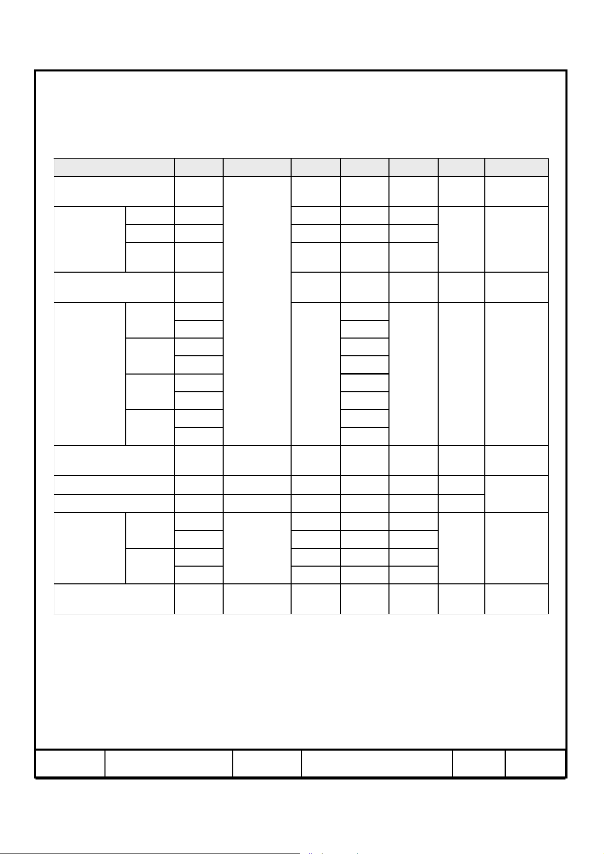
1. Absolute Maximum Ratings
If the condition exceeds maximum ratings, it can cause malfunction or unrecoverable
damage to the device.
NoteUnitMax.Min.SymbolItem
Power Supply Voltage
Storage temperature
Operating Temperature
Panel surface temperature
Shock ( non - operating )
Vibration ( non - operating )
Note (1) Ta= 25 ± 2 °C
(2) Temperature and relative humidity range are shown in the figure below.
a. 93.8 % RH Max. (Ta ≤ 40 °C)
b. Maximum wet-bulb temperature at 40 °C or less. (Ta ≤ 40 °C)
c. No condensation
(3) Polarizer will not be damaged in this range, even though abnormal visual problems occur
T
in
(4) 11ms, sine wave, one time for ±X, ±Y, ±Z axis
(5) 10-300 Hz, Sweep rate 10min, 30min for X,Y,Z axis
SUR
range.
DD
STG
OPR
SUR
NOP
NOP
65-20T
500T
650T
50
℃
℃
℃
(1)V13GND-0.5V
(2)
(2)
(3)
(4)G-S
(5)G1.5-V
(40, 93.8)
(50, 50.4)
Fig. Temperature and Relative humidity range
(65, 27.7)
5/ 33Page05-001-S-100511Doc. NoLTY[Z]460HJ02MODEL
Page 5
2. Optical Characteristics
The optical characteristics should be measured in a dark room or equivalent.
Measuring equipment : TOPCON BM-7,SPECTRORADIOMETER SR-3
(Ta = 25 ± 2°C, VDD=12V, fv= 60Hz, f
=148.5MHz, Dim = 100%)
DCLK
NoteUnitMax.Typ.Min.ConditionSymbolItem
Contrast Ratio
(Center of screen)
Response
Time
Luminance of White
(Center of screen)
Color
Chromaticity
(CIE 1931)
Rising
Falling
G-to-G
[AVE]
Red
Green
Blue
White
Tg
Rx
-5000*2500C/R
(3)
SR-3
138-Tr
86-Tf
msec
(5)
BM-7
-6.5-
L
L,R=0
U,D=0
Viewing
Angle
TYP.
-0.03
0.618
0.333Ry
0.315Gx
0.628Gy
0.155Bx
Normal
-400320Y
TYP.
+0.03
cd/m
2
(6)
SR-3
(7),(8)
SR-3
0.050By
0.280Wx
0.290Wy
%-72--Color Gamut
(7)
SR-3
Gamma
Hor.
Viewing
Angle
Ver.
Brightness Uniformity
(9 Points)
K-10000--Color Temperature
γ
L
R
U
D
uni
C/R≥10
-2.2-
-8979
-8979
Degree
-8979
-8979
%30--B
(7)
SR-3
(8)
SR-3
(4)
SR-3
* marked Items Value does not Specification above when “White stain” occurs at Center Point [Point ⑤ of Note 2.]
Note (1) Test Equipment Setup
The measurement should be executed in a stable, windless and dark room between
40min and 60min after lighting the back light at the given temperature for stabilization
of the back light. This should be measured in the center of screen.
Single lamp current @ Vdim = 100%
Environment condition : Ta = 25 ± 2 °C
6/ 33Page05-001-S-100511Doc. NoLTY[Z]460HJ02MODEL
Page 6
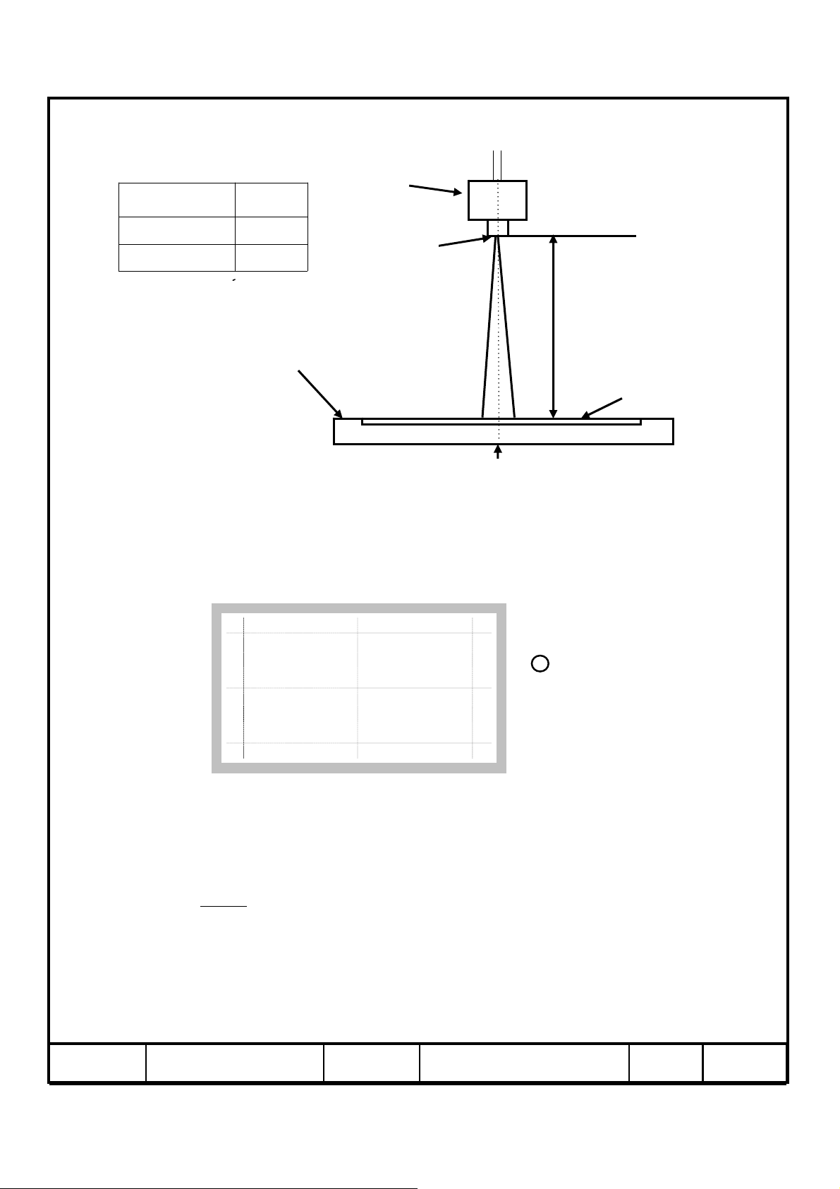
Field Photo detector
1°SR-3
2°BM-7
TFT - LCD Module
Note (2) Definition of test point
320 960 1600
Photo detector
Field
SR-3 : 50㎝
BM-7 : 50㎝
LCD Panel
The center of the screen
180
540
900
Note (3) Definition of Contrast Ratio (C/R)
: Ratio of gray max (Gmax) & gray min (Gmin) at the center point ⑤ of the panel
CR
/
⑨
⑥
G
max
G
min
Gmax : Luminance with all pixels white
Gmin : Luminance with all pixels black
⑧
⑤④
⑦
①②③
Active Area
Test Point
7/ 33Page05-001-S-100511Doc. NoLTY[Z]460HJ02MODEL
Page 7
Note (4) Definition of 9 points brightness uniformity
Buni
BB
(max min)
100
B
max
Bmax : Maximum brightness
Bmin : Minimum brightness
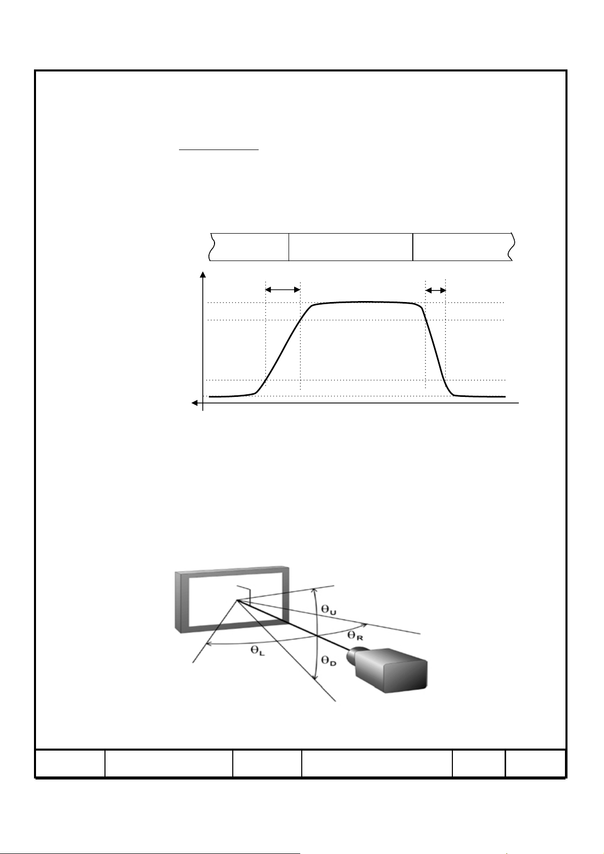
Note (5) Definition of Response time : Sum of Tr, Tf
Display data
Optical Instruments
Response
100%
Black (data off)
T
R
White (data on)
90%
10%
0%
White (data off)
T
F
TIME
Note (6) Definition of Luminance of White : Luminance of white at center point ⑤
Note (7) Definition of Color Chromaticity (CIE 1931)
Color coordinate of Red, Green, Blue & White at center point ⑤
Note (8) Definition of Viewing Angle
: Viewing angle range (C/R ≥10)
8/ 33Page05-001-S-100511Doc. NoLTY[Z]460HJ02MODEL
Page 8
3. Electrical Characteristics
3.1 TFT LCD Module
The connector for display data & timing signal should be connected.
Ta = 25°C ± 2 °C
NoteUnitMax.Typ.Min.SymbolItem
Voltage of Power Supply
(a) Black
Current
of Power
Supply
DD
1200100012001000-(b) White
I
DD
12001000-(c) Mosaic
18001600-(4) Max Pattern
Vsync Frequency
Hsync Frequency
Main Frequency
Rush Current
V
H
DCLK
RUSH
kHz-67.5-f
MHz-148.5-f
Note (1) The ripple voltage should be controlled under 10% of VDD.
(2) f
V=60Hz, fDCLK = 148.5MHz, V
= 12.0V, DC Current.
DD
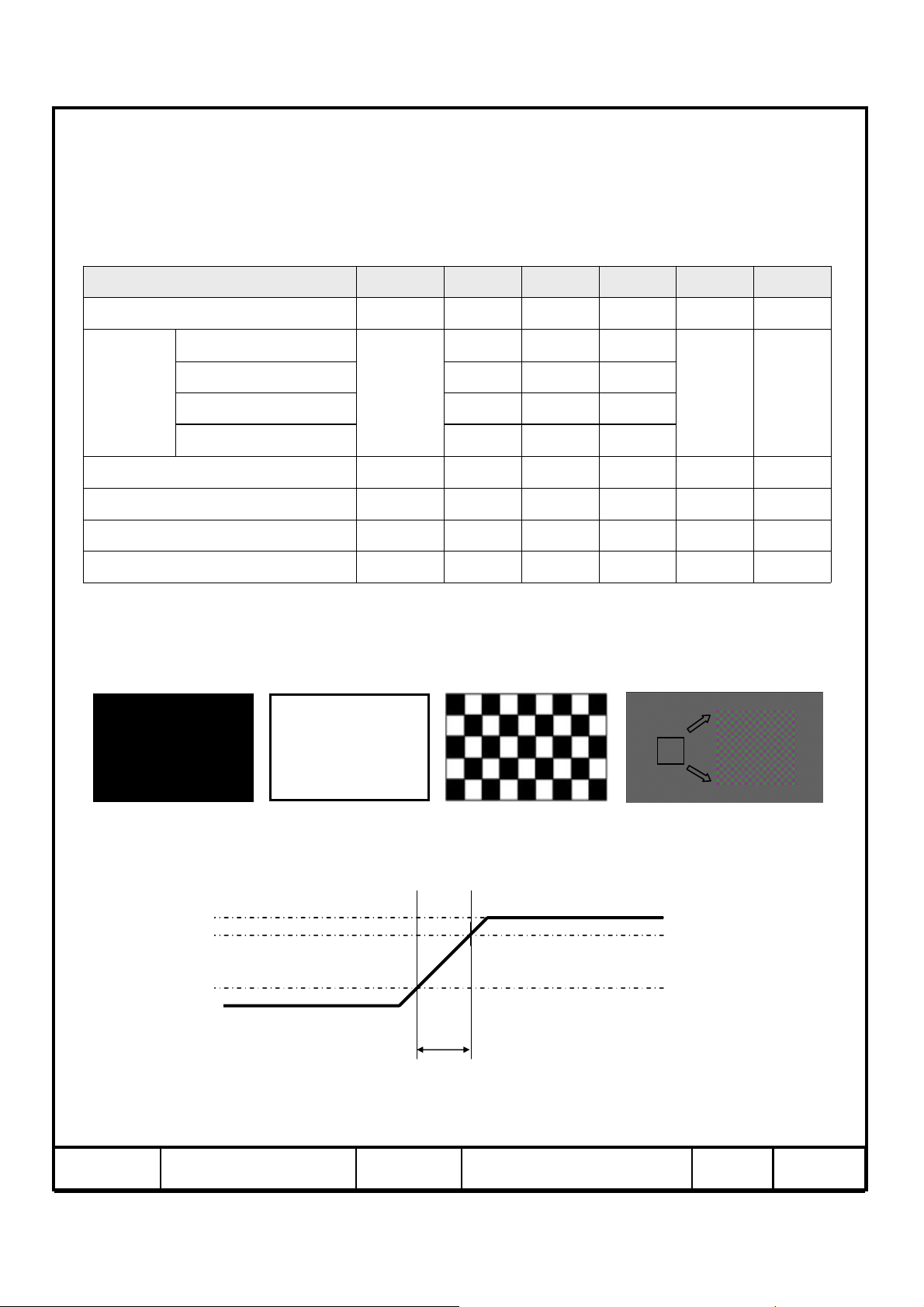
(3) Power dissipation check pattern (LCD Module only)
a) Black Pattern b) White Pattern c) Mosaic d)Max. Pattern
(1)V131211V
(2),(3)mA
Hz-60-f
(4)A5--I
(4) Measurement Conditions
100%
90%
10%
GND
Rush Current I
can be measured when T
RUSH
T
RUSH
=1ms
RUSH
. is1ms
V
DD
9/ 33Page05-001-S-100511Doc. NoLTY[Z]460HJ02MODEL
Page 9
3.2 Back Light Unit
The back light contains 216 LEDs.
The characteristics of lamps are shown in the following tables.
Ta=25 ± 2°C
NoteUnitMax.Typ.Min.SymbolItem
(1)Hour--30,000HrOperating Life Time
Operating
Current
Operating
Voltage
Continuous
Impulsive
(120Hz/Duty50%)
Continuous
Impulsive
(120Hz/Duty50%)
op
op
op
op
mA185--I
V190--V
/StringmA160--I
@110mA
/Duty100%
54LEDs
/110mA@Tj 25℃
Tj 25℃V205--V
Note (1) It is defined as the time to take until the brightness reduces to 50% of its original value.
[Definition of Operating Voltage : At each Strings, I
= 110.0 mArms (typ.)]
op
10 / 33Page05-001-S-100511Doc. NoLTY[Z]460HJ02MODEL
Page 10
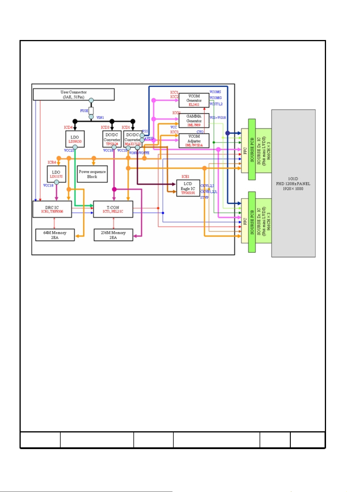
4. Block Diagram
11 / 33Page05-001-S-100511Doc. NoLTY[Z]460HJ02MODEL
Page 11

5. Input Terminal Pin Assignment
5.1. Input Signal & Power (Stand Alone Mode)
5.1.1 Pin Connector : JAE(FI-RE51S)
SignalPIN No.
Power1
Description
VDD
VDD
VDD
VDD
V
DD
N.C.
GND
GND
GND
Odd LVDS Signal -
Odd LVDS Signal +
Odd LVDS Signal -
Odd LVDS Signal +
Odd LVDS Signal -
Odd LVDS Signal +
PIN
No.
Signal
RE[0]P26
RE[1]N27Power2
RE[1]P28Power3
RE[2]N29Power4
RE[2]P30Power5
GND31N.C.6
RECLK-32GND7
RECLK+33GND8
GND34GND9
RE[3]N35RO[0]N10
RE[3]P36RO[0]P11
RE[4]N37RO[1]N12
RE[4]P38RO[1]P13
GND39RO[2]N14
SCL40RO[2]P15
Description
Even LVDS Signal +
Even LVDS Signal -
Even LVDS Signal +
Even LVDS Signal -
Even LVDS Signal +
GND
Even LVDS Clock-
Even LVDS Clock+
GND
Even LVDS Signal -
Even LVDS Signal +
Even LVDS Signal -
Even LVDS Signal +
GND
I2C SCL
GND
Odd LVDS CLK -
Odd LVDS CLK +
GND
Odd LVDS Signal -
Odd LVDS Signal +
Odd LVDS Signal -
Odd LVDS Signal +
GND
Even LVDS Signal -
SDA41GND16
VSYNC42ROCLK-17
B_INT43ROCLK+18
N.C.44GND19
N.C.45RO[3]N20
SA_MODE46RO[3]P21
N.C.47RO[4]N22
N.C.48RO[4]P23
N.C.49GND24
TCON_RDY50RE[0]N25
SEL151
I2C SDA
Balance board
Sync Signal
Bus Switching
N.C.
N.C.
SA Mode Sel Signal
N.C.
N.C.
N.C.
T-Con Ready
SEC Internal Use Only
12 / 33Page05-001-S-100511Doc. NoLTY[Z]460HJ02MODEL
Page 12

5.1. Input Signal & Power (SET Mode)
5.1.1 Pin Connector : JAE(FI-RE51S)
SignalPIN No.
Description
PIN
No.
Signal
Description
N.C.1
Odd LVDS Signal +
Odd LVDS Signal +
Odd LVDS Signal +
N.C.
N.C.
N.C.
N.C.
N.C.
N.C.
GND
GND
GND
Odd LVDS Signal -
Odd LVDS Signal -
Odd LVDS Signal -
GND
Odd LVDS CLK -
RE[0]P26
RE[1]N27N.C.2
RE[1]P28N.C.3
RE[2]N29N.C.4
RE[2]P30N.C.5
GND31N.C.6
RECLK-32GND7
RECLK+33GND8
GND34GND9
RE[3]N35RO[0]N10
RE[3]P36RO[0]P11
RE[4]N37RO[1]N12
RE[4]P38RO[1]P13
GND39RO[2]N14
SCL40RO[2]P15
SDA41GND16
VSYNC42ROCLK-17
Even LVDS Signal +
Even LVDS Signal -
Even LVDS Signal +
Even LVDS Signal -
Even LVDS Signal +
GND
Even LVDS Clock-
Even LVDS Clock+
GND
Even LVDS Signal -
Even LVDS Signal +
Even LVDS Signal -
Even LVDS Signal +
GND
I2C SCL
I2C SDA
Balance board
Sync Signal
Odd LVDS CLK +
GND
Odd LVDS Signal -
Odd LVDS Signal +
Odd LVDS Signal -
Odd LVDS Signal +
GND
Even LVDS Signal -
5.1.2 JST 4PIN CONNECTOR (SM04B-PASS)
PIN No.
1
2
3
4
Signal
Power
Power
GND
GND
Description
VDD
V
DD
GND
GND
B_INT43ROCLK+18
N.C.44GND19
N.C.45RO[3]N20
SA_MODE46RO[3]P21
N.C.47RO[4]N22
N.C.48RO[4]P23
N.C.49GND24
TCON_RDY50RE[0]N25
SEL151
Bus Switching
N.C.
N.C.
SA Mode Sel Signal
N.C.
N.C.
N.C.
T-Con Ready
SEC Internal Use Only
13 / 33Page05-001-S-100511Doc. NoLTY[Z]460HJ02MODEL
Page 13

■ Option Pin Description
■ B _INT : I2C BUS Switching Pull down 100Ω/10kΩ
SDA/SCL LINE BECOME HI-ZL/OPEN
USER CAN ACCESS EEPROMH
■ SA_MODE : Direct 1kΩ
DescriptionOperation
SET MODELow
SA_MODEHigh
■ TCON_RDY : Direct 100Ω
DescriptionOperation
Normal OperationLow High
Error OperationHigh Low
■ SCL : Pull up 220Ω/3.3kΩ
■ SDA : Pull up 220Ω/3.3kΩ
■ V SYNC : Direct 100Ω
■ DCC Table
DescriptionLUT No.
for 120HzDCC1
for 120Hz @ Low temp.DCC2
Not useDCC3, 4
for 100HzDCC5
for 100Hz @ Low temp.DCC6
Not useDCC7
DCC offDCC8
14 / 33Page05-001-S-100511Doc. NoLTY[Z]460HJ02MODEL
Page 14

Note(1) Pin number starts from Right side
Pin No. 1
Pin No. 4
▼
A. 51 Pin
#1
#1
PCB
▼
Pin No. 1 Pin No. 51
#51
connect name
#51
B. 4 Pin
#1
#4
connect name
#1
#4
Fig. Connector diagram
a. All GND pins should be connected together and also be connected to the LCD’s
metal chassis.
b. All power input pins should be connected together.
c. All NC pins should be separated from other signal or power.
15 / 33Page05-001-S-100511Doc. NoLTY[Z]460HJ02MODEL
Page 15

5.2 Input Pin Configuration
■ 4pin : DC Voltage Connector : 51103-0400 (Molex)
Pin Configuration (Function)Pin No.
1 Channel DC Voltage1
2 Channel DC Voltage2
No Connection3
No Connection4
■ 5pin : Feedback Voltage Connector : 51103-0500 (Molex)
Pin Configuration (Function)Pin No.
1 Channel Feedback1
2 Channel Feedback2
No Connection3
No Connection4
No Connection5
16 / 33Page05-001-S-100511Doc. NoLTY[Z]460HJ02MODEL
Page 16

5.3 LVDS Interface
TxOUT/RxIN0
TxOUT/RxIN1
Odd DataLVDS pin
R4TxIN/RxOUT0
R5TxIN/RxOUT1
R6TxIN/RxOUT2
R7TxIN/RxOUT3
R8TxIN/RxOUT4
R9TxIN/RxOUT6
G4TxIN/RxOUT7
G5TxIN/RxOUT8
G6TxIN/RxOUT9
G7TxIN/RxOUT12
G8TxIN/RxOUT13
G9TxIN/RxOUT14
B4TxIN/RxOUT15
B5TxIN/RxOUT18
B6TxIN/RxOUT19
B7TxIN/RxOUT20
Even Data
R4
R5
R6
R7
R8
R9
G4
G5
G6
G7
G8
G9
B4
B5
B6
B7
TxOUT/RxIN2
TxOUT/RxIN3
TxIn/RxIn4
B8TxIN/RxOUT21
B9TxIN/RxOUT22
HSYNCTxIN/RxOUT24
VSYNCTxIN/RxOUT25
DENTxIN/RxOUT26
R2TxIN/RxOUT27
R3TxIN/RxOUT5
G2TxIN/RxOUT10
G3TxIN/RxOUT11
B2TxIN/RxOUT16
B3TxIN/RxOUT17
RESERVEDTxIN/RxOUT23
R0TxIn/RxOUT28
R1TxIn/RxOUT29
G0TxIn/RxOUT30
G1TxIn/RxOUT31
B0TxIn/RxOUT32
B8
B9
HSYNC
VSYNC
DEN
R2
R3
G2
G3
B2
B3
RESERVED
R0
R1
G0
G1
B0
B1TxIn/RxOUT33
RESERVEDTxIn/RxOUT34
B1
RESERVED
17 / 33Page05-001-S-100511Doc. NoLTY[Z]460HJ02MODEL
Page 17

5.4 Input Signals, Basic Display Colors and Gray Scale of Each Color
DATA SIGNAL
COLOR
BASIC
COLOR
GRAY
SCALE
OF
RED
DISPLAY
(10bit)
DARK
↑
↓
LIGHT
R
R
R
R6R5R4R3R2R1R
7
9
0
:
8
0
0
0
0
0
0
0
0
1
0
1
1
1
1
1
1
0
0
0
0
0
0
1
1
1
1
1
1
G
G1G
2
0
111111111WHITE
3
0
0
1
111100000000CYAN
1
0
0
1
1
0
0
0
0
0
0
0000011111111RED
G
G8G7G6G5G4G
B1B
9
0
0
0
1
1
0
0
1
1
0
0
0
0
0
0
BLUEGREENRED
B
2
3
0
1
0
1
0
1
0
1
0
0
0
0
0
0
GRAY
SCALE
B
B5B4B
6
7
0
1
0
1
0
1
0
1
0
0
0
:::::::::::::::::
::::::::::::::::::
0
0
0
LEVEL
B9B8B
-000000000000000000000000BLACK
-111111110000000000000000BLUE
-000000001111111100000000GREEN
-111111111111
-000000000000000011111111RED
-111111110000000011111111MAGENTA
-000000001111111111111111YELLOW
-111111111111111
R0000000000000000000000000BLACK
R1000000000000000000000001
R2000000000000000000000010
R3~
R1020
R1021000000000000000011111101
R1022000000000000000011111110
R102300000000000
GRAY
SCALE
OF
GREEN
GRAY
SCALE
OF
BLUE
DARK
↑
↓
LIGHT
DARK
↑
↓
LIGHT
Note) Definition of Gray :
Rn : Red Gray, Gn : Green Gray, Bn : Blue Gray (n = Gray level)
Input Signal : 0 = Low level voltage, 1 = High level voltage
0
0
0
0
0
0
:::::
0
0
0
0
0
0
0
0
0
0
0
0
0
0
0
0
0
0
0
0
0
:
:
1
1
1
0
0
0
:
:
0
0
0
:::::::::::
0
0
0
1
1
1
0
0
0
0
0
0
0
0
0
0
0
0001111111100000000GREEN
0
0
0
0
:
:
1
1
1
0
0
0
::::::::::::
:::::::::::::::::
0
0
0
0
0
0
:::::
::::::::::::::::
1
1
1
G0000000000000000000000000BLACK
G1000000000000000100000000
G2000000000000001000000000
G3~
G1020
G1021000000001111110100000000
G1022000000001111111000000000
G102300000
B0000000000000000000000000BLACK
B1000000010000000000000000
B2000000100000000000000000
B3~
B1020
B1021111111010000000000000000
B1022111111100000000000000000
B1023111111110000000000000000BLUE
18 / 33Page05-001-S-100511Doc. NoLTY[Z]460HJ02MODEL
Page 18

6. EDID Information
6.1 EEPROM Data
EEPROM Data
RemarkDataAddressSpecItemNo
Panel Product
1
Vender
2 Screen Size XX 01 XX 16進
3 H-Resolution XXXX 02,03 XX,XX 16進
4 V-Resolution XXX 04,05 XX,XX 16進
Vertical
5
Frequency
6 Data Format XX 07 XX - Note 3
FRC Revision
7
Information
8 Part Number
※ Note 1. ※ Note 2. ※ Note 3.
Data Panel Vender Code
00 HDLCD(SEC)
XXXX 00 XX
XX 06 XX - Note 2
XED XX
XX,XX,XX,XX,XX,
XXX(X)XXXXX
XX
Data V-Frequency
00 50/60Hz
E0~EC
XX,XX,XX,XX,XX,
XX,
XX
,XX,XX,XX,XX
Data Data Format
00 6Bit
SONY Choice
-Note 1
ASCII
-Note 4
ASCII
- Note 5, 6
01 Others
02 Others
03 Others
04 Others
05 Others
※ Note 4.
- FRC Revision Code will be Changed from “00” to “41” (A)
When FRC IC is changed. At First MP. This Code will be “00”
※ Note 5.
- LTY[Z]XXXXXXX Only for SEC Model
※ Note 6.
- Rest of them must be “00” (Null)
01 100/120HZ
02 200/240Hz
01 8Bit
02 10Bit
19 / 33Page05-001-S-100511Doc. NoLTY[Z]460HJ02MODEL
Page 19

6.2 EEPROM Data Map
0123456789ABCDEF
0XXXXXXXXXXXXXXXX0000000000000000
1 00000000000000000000000000000000
2 00000000000000000000000000000000
3 00000000000000000000000000000000
4 00000000000000000000000000000000
5 00000000000000000000000000000000
6 00000000000000000000000000000000
7 00000000000000000000000000000000
8 00000000000000000000000000000000
9 00000000000000000000000000000000
A00000000000000000000000000000000
B00000000000000000000000000000000
C00000000000000000000000000000000
D00000000000000000000000000000000
E XXXXXXXXXXXXXXXXXXXXXXXXXXXX0000
F 00000000000000000000000000000000
20 / 33Page05-001-S-100511Doc. NoLTY[Z]460HJ02MODEL
Page 20

7. Interface Timing
7.1 Timing Parameters
7.1.1 ( Stand Alone mode )
NOTEUnitMAX.TYP.MIN.SYMBOLITEMSIGNAL
Clock
Hsync
Frequency
Vsync
Active
Display
Vertical
Period
Display Term
Vertical
Total
Active
Display
Horizontal
Period
Display Term
Horizontal
Total
7.1.2 (SET mode for 96Hz)
H
V
VD
VB
HD
H
C
-MHz148.5148.5148.51/T
-KHz67.567.567.5F
-Hz606060F
-lines108010801080T
-Lines112511251125T
-clocks192019201920T
-clocks220022002200T
NOTEUnitMAX.TYP.MIN.SYMBOLITEMSIGNAL
Clock
Hsync
Vsync
Frequency
C
H
V
-MHz150148.51471/T
-KHz68.6767.9967.31F
-Hz49.5048.0146.54F
Active
-lines108010801080T
Vertical
Display
Period
VD
Display Term
Vertical
Total
VB
-Lines144614161386T
Active
-clocks192019201920T
Horizontal
Display
Period
HD
Display Term
Horizontal
Total
H
-clocks218421842184T
Note) (1) Test Point : TTL control signal and CLK at LVDS Tx input terminal in system
(2) Internal VDD = 3.3V
21 / 33Page05-001-S-100511Doc. NoLTY[Z]460HJ02MODEL
Page 21

7.1.3 ( Set mode for 100Hz)
NOTEUnitMAX.TYP.MIN.SYMBOLITEMSIGNAL
Clock
Hsync
Frequency
Vsync
Active
Display
Vertical
Period
Display Term
Vertical
Total
Active
Display
Horizontal
Period
Display Term
Horizontal
Total
7.1.4 ( SET mode for 120Hz)
Clock
H
V
VD
VB
HD
H
C
-MHz150148.51471/T
-KHz68.6767.9967.31F
-Hz51.0249.9948.98F
-lines108010801080T
-Lines137413601346T
-clocks192019201920T
-clocks218421842184T
NOTEUnitMAX.TYP.MIN.SYMBOLITEMSIGNAL
C
-MHz150148.51471/T
Hsync
Vsync
Frequency
H
V
-KHz68.6767.9967.31F
-Hz61.0859.9659.88F
Active
Vertical
Display
Period
VD
-lines108010801080T
Display Term
Vertical
Total
VB
-Lines114411341124T
Active
-clocks192019201920T
Horizontal
Display
Period
HD
Display Term
Horizontal
Total
H
-clocks218421842184T
Note) (1) Test Point : TTL control signal and CLK at LVDS Tx input terminal in system
(2) Internal VDD = 3.3V
22 / 33Page05-001-S-100511Doc. NoLTY[Z]460HJ02MODEL
Page 22

7.2 Timing diagrams of interface signal
TV
VSYNC
HSYNC
DE
HSYNC
DE
DCLK
DATA
SIGNALS
Sync Width
Sync Width
TVB TVF
1 2 3 n
TH
THB THF
TVD
THD
TC
DCLK
DISPLAY
DATA
DE
TC
TCH
TDS TDH
TES
TCL
0.5
V
0.5
V
CC
0.5
V
CC
CC
23 / 33Page05-001-S-100511Doc. NoLTY[Z]460HJ02MODEL
Page 23

7.3 Power ON/OFF Sequence
To prevent a latch-up or DC operation of the LCD Module, the power on/off
sequence should be as the diagram below.
VDD
(Panel 12V)
EDID Read
LVDS-Rx
FRC_RST(FIXED)
TCON_RDY
VSYNC
DCC_LUT
BL_ON
T1
90%
10%
T2
T4
T5
※ After T3 time don’t access EDID.
T3
T6
T7
T8
T10
90%
10%
T13
T14
T12
T9T9
T11
90%
Unit (ms)
T1
T2
T3
T4
T5
Min
0.47
0
0
200
35
Max
10
100
100
300
75
T6
T7
T8
T9
T10
Min
0
0
0
0
500
Max
450
-
-
-
-
T11
T12
T13
T14
Min
100
45
0
1000
Max
-
-
300
-
The supply voltage of the external system for the Module input should be the same
as the definition of V
DD
.
Apply the lamp voltage within the LCD operation range. When the back light turns on
before the LCD operation or the LCD turns off before the back light turns off,
the display may momentarily show abnormal screen.
In case of V
= off level,
DD
please keep the level of input signals low or keep a high impedance.
T14 should be measured after the Module has been fully discharged between power off
and on period.
Interface signal should not be kept at high impedance when the power is on.
24 / 33Page05-001-S-100511Doc. NoLTY[Z]460HJ02MODEL
Page 24

Page 25

Outline dimension(Rear View)
MODEL LTY[Z]460HJ02 Doc. No
05-001-S-100511
Page
26 / 33
Page 26

9. EMI Specification
: -3dB at CISPR22 Class B
This EMI Recommendation is recommended to be measured as SET Condition.
10. UL Approval
27 / 33Page05-001-S-100511Doc. NoLTY[Z]460HJ02MODEL
Page 27

11. Reliability Test
QuantityTest conditionItem
Temperature
Step Stress
ESD
(non-operation)
ESD(operation)
contact : ±8 kV ,150㎊/330Ω,210Point,1 time/Point
non-contact : ±15 kV,150㎊/330Ω,100Point,1 time/Point
4EA0 ∼ 50℃,10Cycle determination
8EA50℃, 1000hr (500hr determination)HTOL
4EA0℃, 1000hr (500hr determination)LTOL
4EA20 ℃, continue ~RTOL
4EA70℃, 1000hr (500hr determination)HTS
4EA-30℃,1000hr (500hr determination)LTS
4EA40℃ / 95%RH,1000hr (500hr determination)THB
4EA60℃ / 75%RH, 1000hr (500hr determination)WHTS
4EA-20 ℃ ~ 60 ℃, 200cycle (100cycle determination)T/C
3EA±10 kV,200㎊/100 Ω,9Point,3times/Point
3EA
3EAcontact : ±2kV,200㎊/100,Input Con.Pin,3 times/PinInput Con. ESD
POWER
ON/OFF
PALLET
Vibration
4EA30sec (on) / 30sec(off) : 12,000 times
3EA10~300Hz/1.5G/10minSR, XYZ, 30min/axis Vibration
3EACondition : 11msec, ±XY/axis 40G &±Z 1time/axis 30GShock
1PALLET(17EA)1.05 Grms, 2~200Hz, Random, Z axis 1Hr
1PALLET(17EA)20cm, Bottom, Front, Rear 1timesPALLET Drop
[ Result Evaluation Criteria]
Under the display quality test conditions with normal operation state, these shall
be no change which may affect practical display function.
HTOL/ LTOL : High/Low Temperature Operating Life,
THB : Temperature Humidity Bias
HTS/LTS : High/Low Temperature Storage
WHTS : Wet High Temperature Storage
28 / 33Page05-001-S-100511Doc. NoLTY[Z]460HJ02MODEL
Page 28

12. PACKING
12.1 CARTON (Internal Package)
(1) Packing Form
Corrugated fiberboard box and corrugated cardboard as shock absorber
(2) Packing Method
Packing Pallet Box
Cushion Set
Module (17EA)
8.2 Packing Specification
LCD Packing
17 ea / (Packing-
Pallet Box)
215.11kgTotal Pallet Weight
Direction be able to Open
Pallet
RemarkSpecificationItem
1. 192.1Kg/LCD(17ea)
2. 7kg/Cushion Set(2ea)
3. 6.7kg/Packing-Pallet Box(1ea)
4. Cushion Material : EPS
5. Packing Pallet Box Material : DW4
10g/ea, Cobalt-dichloride-free3ea/LCDDesiccant (Drier)
Pallet weight : 8.8kg1 Box / PalletPallet
-VerticalPacking Direction
1150mm(H) x 985mm(V) x 849mm(Height)H x V x heightTotal Pallet Size
Pallet(8.8kg) + Module(11.3 x 17 = 192.1kg)
+ Cushion(7kg) + Pallet-BOX(6.7kg) +
Desiccant(0.03kg x 17 = 0.51kg)
29 / 33Page05-001-S-100511Doc. NoLTY[Z]460HJ02MODEL
Page 29

13. MARKING & OTHERS
A nameplate bearing followed by is affixed to a shipped product at the specified
location on each product.
(1) Parts number : LTY[Z]460HJ02-XXX
(2) Revision: One letters
(3) Lot number : X X X X XXX XX X
Cell Position No. (In the Glass)
Glass No. (In the one Lot)
Lot No. (Glass)
Month
Year (Note1)
Product code
(4) Nameplate Indication
LTY[Z]460HJ02
XXXXXX
XXXXXXXXXX xxx
Line
Week code : 05 29
40mm
Revision code
week
year
LTY[Z]460HJ02XXX
80mm
(5) Packing box attach
100mm
LTY[Z]460HJ02-XXX
XXXX
17
0703
(6) Others
1. After service part
Lamps cannot be replaced because of the narrow bezel structure.
Lot number
Part number
Revision code
Box serial number
30 / 33Page05-001-S-100511Doc. NoLTY[Z]460HJ02MODEL
Page 30

14. General Precautions
14.1 Handling
(a) When the Module is assembled, it should be attached to the system firmly
using all mounting holes. Be careful not to twist and bend the Module.
(b) Because the inverter use high voltage, it should be disconnected from power
before it is assembled or disassembled.
(c) Refrain from strong mechanical shock and / or any force to the Module.
In addition to damage, this may cause improper operation or damage to the Module
and CCFT back light.
(d) Note that polarizers are very fragile and could be damage easily.
Do not press or scratch the surface harder than a HB pencil lead.
(e) Wipe off water droplets or oil immediately. If you leave the droplets for a long
time, staining or discoloration may occur.
(f) If the surface of the polarizer is dirty, clean it using absorbent cotton or soft cloth.
(g) Desirable cleaners are water, IPA(Isopropyl Alcohol) or Hexane.
Do not use Ketone type materials(ex. Acetone), Ethyl alcohol, Toluene, Ethyl acid
or Methyl chloride. It might permanent damage to the polarizer due to chemical
reaction.
(h) If the liquid crystal material leaks from the panel, it should be kept away
from the eyes or mouth . In case of contact with hands, legs or clothes, it must
be washed away with soap thoroughly.
(i) Protect the Module from static, or the CMOS Gate Array IC would be damaged.
(j) Use finger-stalls with soft gloves in order to keep display clean during the
incoming inspection and assembly process.
(k) Do not disassemble the Module.
(l) Do not pull or fold the lamp wire.
(m) Do not adjust the variable resistor located on the Module.
(n) Protection film for polarizer on the Module should be slowly peeled off just before use
so that the electrostatic charge can be minimized.
(o) Pins of I/F connector should not be touched directly with bare hands.
31 / 33Page05-001-S-100511Doc. NoLTY[Z]460HJ02MODEL
Page 31

14.2 Storage
(a) Do not leave the Module in high temperature, and high humidity for a long time.
It is highly recommended to store the Module with temperature from 0 to 35℃
and relative humidity of less than 70%.
(b) Do not store the TFT- L CD Module in direct sunlight.
(c) The Module should be stored in a dark place. It is prohibited to apply sunlight or
fluorescent light in storing.
14.3 Operation
(a) No Connection or disconnect the Module in the "Power On" condition.
(b) Power supply should always be turned on/off by the "Power on/off sequence"
(c) Module has high frequency circuits. Sufficient suppression to the electromagnetic
interference should be done by system manufacturers. Grounding and shielding methods
may be important to minimize the interference.
(d) The cable between the back light connector and its inverter power supply should
be connected directly with a minimized length. A longer cable between
the back light and the inverter may cause lower luminance of lamp(CCFT) and
may require higher startup voltage(Vs).
14.4 Operation Condition Guide
(a) The LCD product should be operated under normal conditions.
Normal condition is defined as below;
- Temperature : 20±15℃
- Humidity : 55±20%
- Display pattern : continually changing pattern (Not stationary)
(b) If the product will be used in extreme conditions such as high temperature,
humidity, display patterns or operation time etc.., It is strongly recommended
to contact SEC for Application engineering advice. Other wise, its reliability and
function may not be guaranteed. Extreme conditions are commonly found at
Airports, Transit Stations, Banks, Stock market, and Controlling systems.
32 / 33Page05-001-S-100511Doc. NoLTY[Z]460HJ02MODEL
Page 32

14.5 Others
(a) Ultra-violet ray filter is necessary for outdoor operation.
(b) Avoid condensation of water. It may result in improper operation or disconnection
of electrode.
(c) Do not exceed the absolute maximum rating value. ( supply voltage variation,
input voltage variation, variation in part contents and environmental temperature,
and so on)
Otherwise the Module may be damaged.
(d) If the Module keeps displaying the same pattern for a long period of time,
the image may be "sticked" to the screen.
To avoid image sticking, it is recommended to use a screen saver.
(e) This Module has its circuitry PCB's on the rear side and should be handled
carefully in order not to be stressed.
(f) Please contact SEC in advance when you display the same pattern for a long time.
33 / 33Page05-001-S-100511Doc. NoLTY[Z]460HJ02MODEL
 Loading...