

Page 1
Contents
Revision History -------------------------------------------------------------------------------------------- (3)
General Description --------------------------------------------------------------------------------------- (4)
General Information --------------------------------------------------------------------------------------- (4)
1. Absolute Maximum Ratings -------------------------------------------------------------------------- (5)
2. Optical Characteristics --------------------------------------------------------------------------------- (7)
3. Electrical Characteristics ------------------------------------------------------------------------------- (10)
3.1 TFT LCD Module
3.2 Back Light Unit
4. Block Diagram ------------------------------------------------------------------------------------------- (12)
5. Input Terminal Pin Assignment --------------------------------------------------------------------- (13)
5.1 Input Signal & Power
5.2 . LS Bar Input Pin Configuration
5.3 LVDS Interface
5.4 Input Signals, Basic Display Colors and Gray Scale of Each Color
6. EDID Information --------------------------------------------------------------------------------------- (19)
6.1 EEPROM Data
6.2 EEPROM Data Map
7. Interface Timing ---------------------------------------------------------------------------------------- (21)
7.1 Timing Parameters (DE only mode)
7.2 Timing Diagrams of interface Signal (DE only mode)
7.3 Power ON/OFF Sequence
8. Outline Dimension -------------------------------------------------------------------------------------- (26)
9. EMI Specification --------------------------------------------------------------------------------------- (33)
10. UL Approval
11. Reliability Test ----------------------------------------------------------------------------------------- (34)
12. Packing ------------------------------------------------------------------------------------------------ (35)
13. Marking & Others ------------------------------------------------------------------------------------- (36)
14. General Precaution ---------------------------------------------------------------------------------- (37)
14.1 Handling
14.2 Storage
14.3 Operation
14.4 Operation Condition Guide
14.5 Others
MODEL LTY[Z]320HQ01 Doc. No 05-000-S-111117 Page / 39
2
Page 2
* Revision History
Date
Nov.
17,
2011
Rev.
No
000 - First Issued
Page Summary
MODEL LTY[Z]320HQ01 Doc. No 05-000-S-111117 Page / 39
3
Page 3
General Description
Description
LTY[Z]320HQ01 is a color active matrix liquid crystal display (LCD) that uses amorphous
silicon TFT(Thin Film Transistor) as switching components. This model is composed of a
TFT LCD panel, a driver circuit and a back light unit. The resolution of a 32.0“ is 1920 x
1080 and this model can display up to 1.07G colors with wide viewing angle of 89° or
higher in all directions. This panel is intended to support applications to provide a excellent
performance for Flat Panel Display such as Home-alone Multimedia TFT-LCD TV, Display
terminals for AV application products, and High Definition TV (HDTV).
Features
RoHS compliance (Pb-free)
High contrast ratio, high aperture ratio, fast response time
SPVA (Super Patterned Vertical Align) mode
Wide viewing angle (±89°)
Full HD (1920 x 1080 pixels) resolution (16:9)
Low Power consumption
WLED (White Light Emitting Diode) Backlight
LVDS (Low Voltage Differential Signaling) interface
General Information
Items Specification Unit Note
Module Size
727.6(H
Weight 5000(Max) g
Pixel Pitch 0.12125(H) * 3 x 0.36375(V) mm
Active Display Area 698.4(H) x 392.85(V) mm
Surface Treatment Haze 0.8%, Hard-coating (2H)
Display Colors 10 bit - 1.07g colors
Number of Pixels 1920 x 1080 pixel
Pixel Arrangement RGB vertical stripe
Display Mode Normally Black
Luminance of White
) x 424.0(V
TYP
25.2(D
450
)
TYP
) Design Value
MAX
mm
cd/m
±0.7mm
2
Typ.
MODEL LTY[Z]320HQ01 Doc. No 05-000-S-111117 Page / 39
4
Page 4
1. Absolute Maximum Ratings
1-1 Operating Condition
If the condition exceeds maximum ratings, it can cause malfunction or unrecoverable
damage to the device.
Item Symbol Min. Max. Unit Note
Power Supply Voltage V
Module Storage temperature T
Operating Temperature T
Panel surface temperature T
Shock ( non - operating ) S
Vibration ( non - operating ) V
Note (1) Ta= 25 ± 2 °C
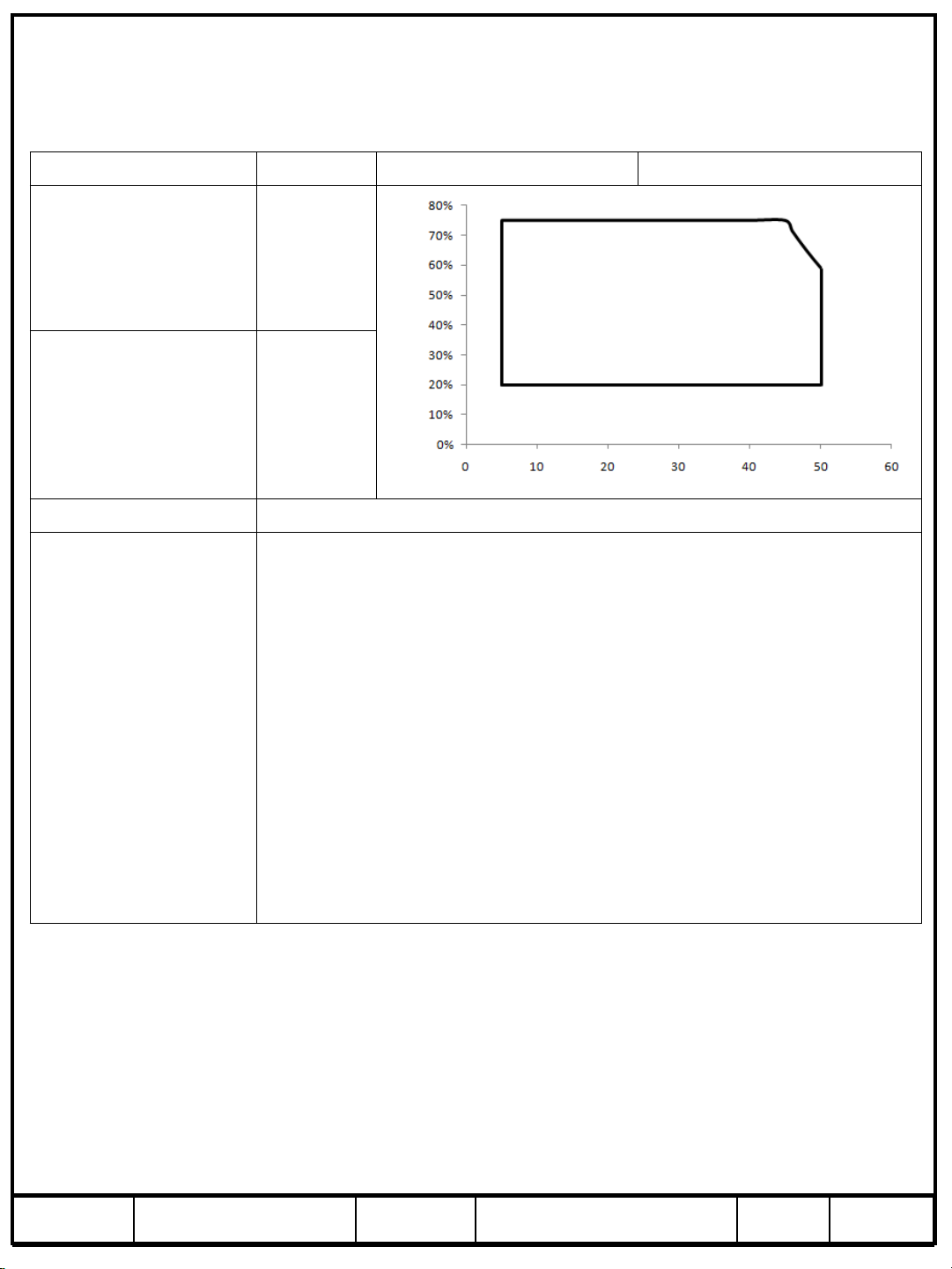
(2) Temperature and relative humidity range are shown in the figure below.
a. 93.8 % RH Max. (Ta ≤ 40 °C)
b. Maximum wet-bulb temperature at 40 °C or less. (Ta ≤ 40 °C)
c. No condensation
(3) Polarizer will not be damaged in this range, even though abnormal visual problems occur
in T
(4) 11ms, sine wave, one time for ±X, ±Y, ±Z axis
(5) 10-300 Hz, Sweep rate 10min, 30min for X,Y,Z axis
SUR
range.
DD
STG
OPR
SUR
NOP
NOP
GND-0.5 13 V (1)
-20 65
0 50
0 65
℃
℃
℃
- 50 G (4)
- 1.5 G (5)
(2)
(2)
(3)
Fig. Temperature and Relative humidity range
MODEL LTY[Z]320HQ01 Doc. No 05-000-S-111117 Page / 39
5
Page 5
1. Absolute Maximum Ratings
1-2 Pallet Storage Condition (Not Included Transportation. ※except for service Panel)
ITEM Unit Min. Max.
(45,75)
Storage Temperature (℃)
(5,75)
(50,59)
Pallet Storage Condition
(5,20)
Storage Humidity (%rH)
Relative Humidity (%RH)
Temperature (℃)
Storage life from S2-In 12 months
- The storage room should provide good ventilation and temperature control.
- Products should not be placed on the floor,
but on the Pallet away from a wall.
- Prevent products from direct sunlight, moisture nor water;
Be cautious of a build up of condensation.
Storage Condition
- Avoid other hazardous environment while storing goods.
- If products delivered or kept in conditions of over the storage period of
3 months, the recommended temperature or humidity range,
we recommend you leave them at a temperature of 20℃ and a humidity
of 50% for 24 hours.
(50,20)
MODEL LTY[Z]320HQ01 Doc. No 05-000-S-111117 Page / 39
6
Page 6
2. Optical Characteristics
The optical characteristics should be measured in a dark room or equivalent.
Measuring equipment : TOPCON BM-7,SPECTRORADIOMETER SR-3
(LED Input Current = 110mA, Ta = 25 ± 2°C, VDD=12V, fv= 60Hz, f
Item Symbol Condition Min. Typ. Max. Unit Note
Contrast Ratio
(Center of screen)
Response
Time
G-to-G
Luminance of White
(Center of screen)
Color
Chromaticity
(CIE 1931)
Rising Tr - - -
Falling Tf - - -
[AVE]
Red
Green
Blue
White
C/R*
3000 5000 -
Tg - 3.5 -
Y
Rx
Ry
Gx
Gy
Bx
By
Wx
Wy
L
Normal
qL,R=0
qU,D=0
Viewing
Angle
380 450 - cd/m
0.641
0.332
0.312
TYP.
-0.03
0.611
0.155
0.053
0.280
0.285
=148.5MHz, Dim = 100%)
DCLK
msec
2
TYP.
+0.03
(3)
SR-3
(5)
BM-7
(6)
SR-3
(7),(8)
SR-3
Color Gamut - - 72 - %
Color Temperature - - 10000 - K
2Point Gamma γ
Hor.
Viewing
Angle
Ver.
Brightness Uniformity
(9 Points)
q
L
q
R
q
U
q
D
B
uni
7G ~ 57G
(Full = 64G)
C/R≥10
1.7 2.2 2.7 (9)
79 89 -
79 89 -
Degree
79 89 -
79 89 -
- - 30 %
* CR = (White at point ⑤ of Note 2) / (Most Dark Point of Black Pattern at area ⓐ of Note 2)
Note (1) Test Equipment Setup
The measurement should be executed in a stable, windless and dark room between
40min and 60min after lighting the back light at the given temperature for stabilization
of the back light. This should be measured in the center of screen.
Single LED current @ Vdim = 100%
Environment condition : Ta = 25 ± 2 °C
(7)
SR-3
(7)
SR-3
(8)
SR-3
(4)
SR-3
MODEL LTY[Z]320HQ01 Doc. No 05-000-S-111117 Page / 39
7
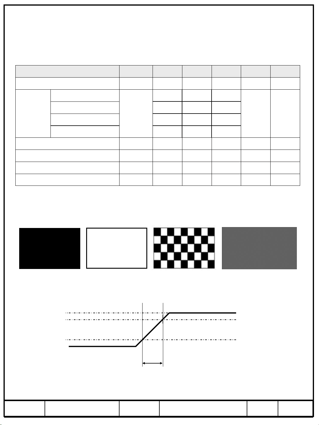
Page 7
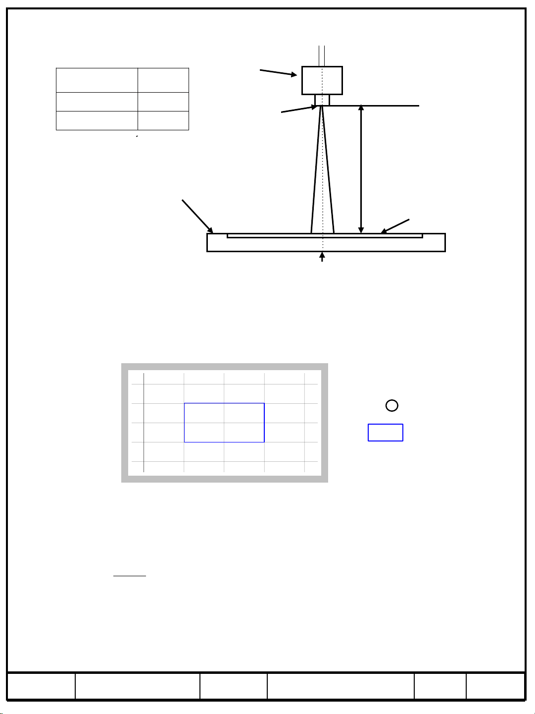
Photo detector Field
C R
G
G
/
max
min
Photo detector
SR-3
BM-7
TFT - LCD Module
Note (2) Definition of test point
320 960 1600
180
1°
2°
⑨
⑧
Field
The center of the screen
⑦
SR-3 : 50㎝
BM-7 : 50㎝
LCD Panel
Active Area
Area ⓐ
540
900
Note (3) Definition of Contrast Ratio (C/R)
: Ratio of gray max (Gmax) & gray min (Gmin) at the center point ⑤ of the panel
MODEL LTY[Z]320HQ01 Doc. No 05-000-S-111117 Page / 39
⑥
⑤ ④
②③
640 1280
Gmax : Luminance with all pixels white
Gmin : Luminance with all pixels black
360
720
①
Test Point
CR Measured Area
8
Page 8
Note (4) Definition of 9 points brightness uniformity
Buni
B B
B
100
( max min)
max
Gamma X Y
X Z B B B
Y Measurement Level Z Measurement Brightness
B Maximum Brightness B Minimum Brightness
lum
lum
log log
: / :
: / :
min max min
max min
100 100
100
Bmax : Maximum brightness
Bmin : Minimum brightness
Note (5) Definition of Response time : Sum of Tr, Tf
Display data
Optical Instruments
Response
Note (6) Definition of Luminance of White : Luminance of white at center point ⑤
Note (7) Definition of Color Chromaticity (CIE 1931)
Color coordinate of Red, Green, Blue & White at center point ⑤
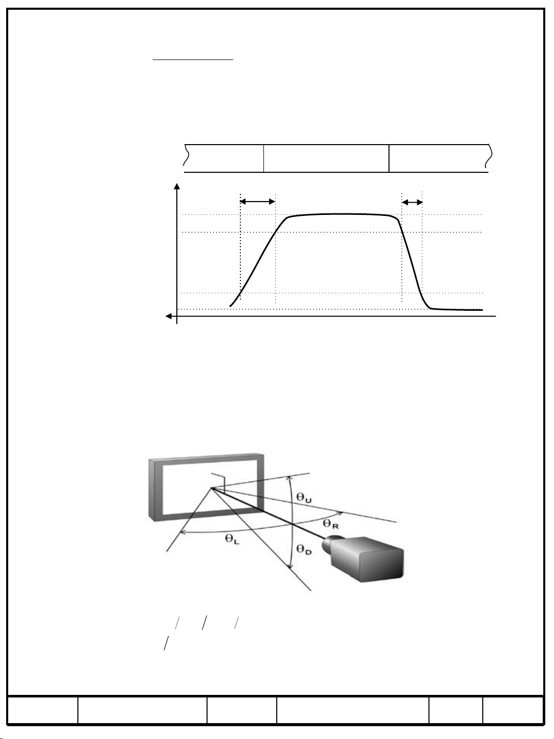
Note (8) Definition of Viewing Angle
: Viewing angle range (C/R ≥10)
100%
90%
10%
0%
Black (data off)
T
R
White (data on)
White (data off)
T
F
TIME
Note (9) Definition of 2 point Gamma
MODEL LTY[Z]320HQ01 Doc. No 05-000-S-111117 Page / 39
9
Page 9
3. Electrical Characteristics
3.1 TFT LCD Module
The connector for display data & timing signal should be connected.
Ta = 25°C ± 2 °C
Item Symbol Min. Typ. Max. Unit Note
Voltage of Power Supply V
(a) Black
Current
(b) White -
of Power
Supply
(c) Mosaic (4) Max Pattern -
Vsync Frequency f
Hsync Frequency f
Main Frequency f
Rush Current I
DD
I
DD
V
H
DCLK
RUSH
11 12 13 V (1)
-
1320
1300
-
1700
mA (2),(3)
1340
1760
-
-
47 60 62 Hz
50 67.5 73 kHz
130 148.5 155 MHz
- - 5 A (4)
Note (1) The ripple voltage should be controlled under 10% of VDD.
(2) fV=60Hz, fDCLK = 148.5MHz, VDD= 12.0V, DC Current.
(3) Power dissipation check pattern (LCD Module only)
a) Black Pattern b) White Pattern c) Mosaic d)Max. Pattern
(4) Measurement Conditions
V
100%
DD
90%
10%
GND
T
=1ms
RUSH
Rush Current I
MODEL LTY[Z]320HQ01 Doc. No 05-000-S-111117 Page / 39
can be measured when T
RUSH
RUSH
. is1ms
10
Page 10
3.2 Back Light Unit
The back light unit contains 60LEDs.
The characteristics of LEDs are shown in the following tables.
Item Symbol Min. Typ. Max. Unit Note
Operating Life Time Hr 30,000 - - Hour (1)
Ta=25 ± 2°C
Operating
Current
Operating
Voltage
Range of Voltage
(Power Consumption)
Note (1) It is defined as the time to take until the brightness reduces to 50% of its original value at
each String, Iop=.110.0mArms
[Definition of Operating Voltage : At each Strings, Iop= 110.0 mArms (typ.)]
Continuous Iop - 110 200 mA
Continuous Vop 171 - 194 V
∇Vf
-
- - 11.5 V @140mA(/String)
(19.36) (22)
30LEDs
/140mA@Ta 25℃
Iop=110mA
@Ta 25℃
3.2.1 Review and Update for Electrical Specification
According to the improvement of efficiency for devices, the electrical specification would be revie
wed and revised after initial values had been established.This revision mentioned above should be
discussed at appropriate time.
MODEL LTY[Z]320HQ01 Doc. No 05-000-S-111117 Page / 39
11
Page 11
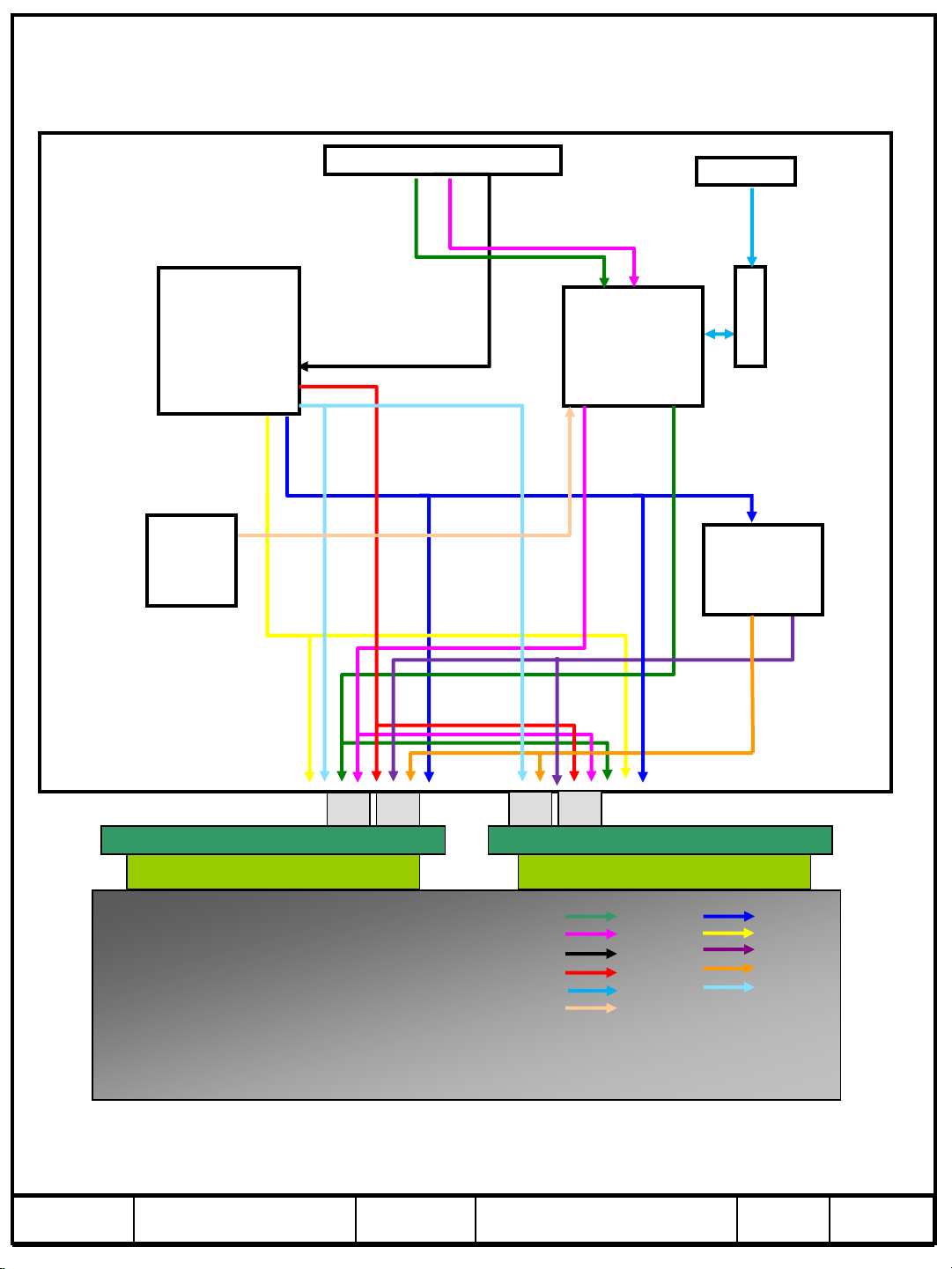
4. Block Diagram
DC/DC
Converter
DC/DC
Converter
User Connector (JAE 51Pin)
JST 14Pin
F-Memory
T-CON
Caraway
Gamma
Merge IC
FFC 68 Pin x 2
Source PCB Source PCB
Source D-IC,8Bit Mini-LVDS,966chⅩ3
Source D-IC,8Bit Mini-LVDS,966chⅩ3
1920Ⅹ1080ⅩRGB
MODEL LTY[Z]320HQ01 Doc. No 05-000-S-111117 Page / 39
FFC 68 Pin x 2
CONTROL
DATA
VIN(12V)
VCC 3.3V
SPI
VCC 1.1V
AVDD
HAVDD
VCOM
Gamma
ASG CLK
12
Page 12
5. Input Terminal Pin Assignment
5.1. Input Signal & Power
1. 51Pin Connector : FI-RNE51SZ-HF (JAE)
PIN No. Signal Description PIN No. Signal Description
1 Vin Power 26 RE[0]P Even LVDS Signal +
2 Vin Power 27 RE[1]N Even LVDS Signal 3 Vin Power 28 RE[1]P Even LVDS Signal +
4 Vin Power 29 RE[2]N Even LVDS Signal 5 Vin Power 30 RE[2]P Even LVDS Signal +
6 N.C. No Connection 31 GND GND
7 GND GND 32 RECLKN Even LVDS CLK -
8 GND GND 33 RECLKP Even LVDS CLK +
9 GND GND 34 GND GND
10 RO[0]N Odd LVDS Signal - 35 RE[3]N Even LVDS Signal 11 RO[0]P Odd LVDS Signal + 36 RE[3]P Even LVDS Signal +
12 RO[1]N Odd LVDS Signal - 37 RE[4]N Even LVDS Signal 13 RO[1]P Odd LVDS Signal + 38 RE[4]P Even LVDS Signal +
14 RO[2]N Odd LVDS Signal - 39 GND GND
15 RO[2]P Odd LVDS Signal + 40 SCL_C I2C SCL
16 GND GND 41 SDA_C I2C SDA
17 ROCLKN Odd LVDS CLK - 42 Option 1 TV SET use only
18 ROCLKP Odd LVDS CLK + 43 BINT Bus Release
19 GND GND 44 Option 2 TV SET use only
20 RO[3]N Odd LVDS Signal - 45 Option 3 TV SET use only
21 RO[3]P Odd LVDS Signal + 46 Option 4 TV SET use only
22 RO[4]N Odd LVDS Signal - 47 Option 5 TV SET use only
23 RO[4]P Odd LVDS Signal + 48 Option 6 TV SET use only
24 GND GND 49 Option 7 TV SET use only
25 RE[0]N Even LVDS Signal - 50 Option 8 TV SET use only
51 Option 9 TV SET use only
MODEL LTY[Z]320HQ01 Doc. No 05-000-S-111117 Page / 39
13
Page 13

2. 14 Pin Connector : 14FLT-SM2-C-TB (JST)
PIN No. Signal Description
1
2
3 /WP SPI_WP
4 /CS SPI_CS
5 CTRL SPI_CTRL
6 GND GND
7 CLK SPI_CLK
8 GND GND
N.C. No Connection
N.C. No Connection
PIN No. Signal Description
■ Option Pin Description
These pins are CMOS interface.
Please use within the range of the following restriction.
VIH:2.4V(min) / 3.5V(max)
VIL:0.0V(min) / 0.4V(max)
9 DO SPI_DO
10 GND GND
11 DI SPI_DI
12 GND GND
13 GND GND
14 GND GND
■ B-INT
Operation Description
Low/OPEN
HIGH USER CAN ACCESS EEPROM
■SCL : Pull up 22Ω/ 2.2kΩ
■SDA : Pull up 22Ω/ 2.2kΩ
USER CAN NOT ACCESS EEPROM
MODEL LTY[Z]320HQ01 Doc. No 05-000-S-111117 Page / 39
14
Page 14

Note(1) Pin number starts from left side
Pin No.1
▼
PCB
▼
Pin No.1 Pin No.51
Fig No1. 51Pin
#1 #51
Fig No2. 14Pin
#1#2
#14
#13
#1
Fig. Connector diagram
#51
a. All GND pins should be connected together and also be connected to the LCD’s
metal chassis.
b. All power input pins should be connected together.
c. All NC pins should be separated from other signal or power.
MODEL LTY[Z]320HQ01 Doc. No 05-000-S-111117 Page / 39
15
Page 15

5.2. LS Bar Input Pin Configuration
1. CONNECTOR : Morex/51103-040
Pin
1
2 N.C.
3 N.C.
4
2. CONNECTOR : Morex/51103-0500
Pin
1
2
3
4
5 N.C.
Pin Configuration (Function)
DC Voltage (+)
DC Voltage (+)
Pin Configuration (Function)
Feedback
N.C.
N.C.
Feedback
MODEL LTY[Z]320HQ01 Doc. No 05-000-S-111117 Page / 39
16
Page 16

5.3 LVDS Interface
TxOUT/RxIN0
TxOUT/RxIN1
TxOUT/RxIN2
TxOUT/RxIN3
TxOUT/RxIN4
LVDS pin Odd Data Even Data
TxIN/RxOUT0 R4 R4
TxIN/RxOUT1 R5 R5
TxIN/RxOUT2 R6 R6
TxIN/RxOUT3 R7 R7
TxIN/RxOUT4 R8 R8
TxIN/RxOUT6 R9 R9
TxIN/RxOUT7 G4 G4
TxIN/RxOUT8 G5 G5
TxIN/RxOUT9 G6 G6
TxIN/RxOUT12 G7 G7
TxIN/RxOUT13 G8 G8
TxIN/RxOUT14 G9 G9
TxIN/RxOUT15 B4 B4
TxIN/RxOUT18 B5 B5
TxIN/RxOUT19 B6 B6
TxIN/RxOUT20 B7 B7
TxIN/RxOUT21 B8 B8
TxIN/RxOUT22 B9 B9
TxIN/RxOUT24 HSYNC HSYNC
TxIN/RxOUT25 VSYNC VSYNC
TxIN/RxOUT26 DEN DEN
TxIN/RxOUT27 R2 R2
TxIN/RxOUT5 R3 R3
TxIN/RxOUT10 G2 G2
TxIN/RxOUT11 G3 G3
TxIN/RxOUT16 B2 B2
TxIN/RxOUT17 B3 B3
TxIN/RxOUT23 Reserved Reserved
TxIN/RxOUT28 R0 R0
TxIN/RxOUT29 R1 R1
TxIN/RxOUT30 G0 G0
TxIN/RxOUT31 G1 G1
TxIN/RxOUT32 B0 B0
TxIN/RxOUT33 B1 B1
TxIN/RxOUT34 Reserved Reserved
MODEL LTY[Z]320HQ01 Doc. No 05-000-S-111117 Page / 39
17
Page 17

5.4 Input Signals, Basic Display Colors and Gray Scale of Each Color
DATA SIGNAL
COLOR
BASIC
COLOR
GRAY
SCALE
OF
RED
DISPLAY
(10bit)
BLACK 0 0 0 0 0 0 0 0 0 0 0 0 0 0 0 0 0 0 0 0 0 0 0 0 0 0 0 0 0 0 -
BLUE 0 0 0 0 0 0 0 0 0 0 0 0 0 0 0 0 0 0 0 0 1 1 1 1 1 1 1 1 1 1 -
GREEN 0 0 0 0 0 0 0 0 0 0 1 1 1 1 1 1 1 1 1 1 0 0 0 0 0 0 0 0 0 0 -
CYAN 0 0 0 0 0 0 0 0 0 0 1 1 1 1 1 1 1 1 1 1 1 1 1 1 1 1 1 1 1 1 -
RED 1 1 1 1 1 1 1 1 1 0 0 0 0 0 0 0 0 0 0 0 0 0 0 0 0 0 0 0 0 0 -
MAGENTA 1 1 1 1 1 1 1 1 1 1 0 0 0 0 0 0 0 0 0 0 1 1 1 1 1 1 1 1 1 1 -
YELLOW 1 1 1 1 1 1 1 1 1 1 1 1 1 1 1 1 1 1 1 1 0 0 0 0 0 0 0 0 0 0 -
WHITE 1 1 1 1 1 1 1 1 1 1 1 1 1 1 1 1 1 1 1 1 1 1 1 1 1 1 1 1 1 1 BLACK 0 0 0 0 0 0 0 0 0 0 0 0 0 0 0 0 0 0 0 0 0 0 0 0 0 0 0 0 0 0 R0
DARK
LIGHT
RED 1 1 1 1 1 1 1 1 1 1 0 0 0 0 0 0 0 0 0 0 0 0 0 0 0 0 0 0 0 0 R1023
R0R1R2R3R4R5R6R7R8R9G0G1G2G3G4G5G6G7G8G9B0B1B2B3B4B5B6B7B8B
1 0 0 0 0 0 0 0 0 0 0 0 0 0 0 0 0 0 0 0 0 0 0 0 0 0 0 0 0 0 R1
0 1 0 0 0 0 0 0 0 0 0 0 0 0 0 0 0 0 0 0 0 0 0 0 0 0 0 0 0 0 R2
↑
: : : : : : : : : : : : : : : : : :
: : : : : : : : : : : : : : : : : :
↓
1 0 1 1 1 1 1 1 1 1 0 0 0 0 0 0 0 0 0 0 0 0 0 0 0 0 0 0 0 0 R1021
0 1 1 1 1 1 1 1 1 1 0 0 0 0 0 0 0 0 0 0 0 0 0 0 0 0 0 0 0 0 R1022
RED GREEN BLUE
GRAY
SCALE
LEVEL
9
R3~
R1020
BLACK 0 0 0 0 0 0 0 0 0 0 0 0 0 0 0 0 0 0 0 0 0 0 0 0 0 0 0 0 0 0 G0
0 0 0 0 0 0 0 0 0 0 1 0 0 0 0 0 0 0 0 0 0 0 0 0 0 0 0 0 0 0 G1
GRAY
SCALE
OF
GREEN
GRAY
SCALE
OF
BLUE
DARK
LIGHT
GREEN 0 0 0 0 0 0 0 0 0 0 1 1 1 1 1 1 1 1 1 1 0 0 0 0 0 0 0 0 0 0 G1023
BLACK 0 0 0 0 0 0 0 0 0 0 0 0 0 0 0 0 0 0 0 0 0 0 0 0 0 0 0 0 0 0 B0
DARK
LIGHT
BLUE 0 0 0 0 0 0 0 0 0 0 0 0 0 0 0 0 0 0 0 0 1 1 1 1 1 1 1 1 1 1 B1023
0 0 0 0 0 0 0 0 0 0 0 1 0 0 0 0 0 0 0 0 0 0 0 0 0 0 0 0 0 0 G2
↑
: : : : : : : : : : : : : : : : : :
: : : : : : : : : : : : : : : : : :
↓
0 0 0 0 0 0 0 0 0 0 1 0 1 1 1 1 1 1 1 1 0 0 0 0 0 0 0 0 0 0 G1021
0 0 0 0 0 0 0 0 0 0 0 1 1 1 1 1 1 1 1 1 0 0 0 0 0 0 0 0 0 0 G1022
0 0 0 0 0 0 0 0 0 0 0 0 0 0 0 0 0 0 0 0 1 0 0 0 0 0 0 0 0 0 B1
0 0 0 0 0 0 0 0 0 0 0 0 0 0 0 0 0 0 0 0 0 1 0 0 0 0 0 0 0 0 B2
↑
: : : : : : : : : : : : : : : : : :
: : : : : : : : : : : : : : : : : :
↓
0 0 0 0 0 0 0 0 0 0 0 0 0 0 0 0 0 0 0 0 1 0 1 1 1 1 1 1 1 1 B1021
0 0 0 0 0 0 0 0 0 0 0 0 0 0 0 0 0 0 0 0 0 1 1 1 1 1 1 1 1 1 B1022
Note) Definition of Gray :
Rn : Red Gray, Gn : Green Gray, Bn : Blue Gray (n = Gray level)
Input Signal : 0 = Low level voltage, 1 = High level voltage
G3~
G1020
B3~
B1020
MODEL LTY[Z]320HQ01 Doc. No 05-000-S-111117 Page / 39
18
Page 18

6. EDID Information
6.1 EEPROM Data
EEPROM Data
No Item Spec Address Data Remark
Panel Product
1
Vender
2 Screen Size 32 01 20
3 H-Resolution 1920 02,03 07,80
4 V-Resolution 1080 04,05 04,38
Vertical
5
Frequency
6 Data Format 10Bit 07 02 - Note 3
FRC Revision
7
Information
8 Part Number LTY320HQ0102 E0~EC
※ Note 1. ※ Note 2. ※ Note 3.
Data Panel Vender Code
00 HDLCD(SEC)
SEC 00 00
200/240Hz 06 02 - Note 2
1st ED 00
4C,54,59,33,32,
30,48,51,30,31,
30,32,00
Data V-Frequency
00 50/60Hz
Data Data Format
00 6Bit
SONY Choice
- Note 1
16進
16進
16進
ASCII
- Note 4
ASCII
- Note 5, 6
01 Others
02 Others
03 Others
04 Others
05 Others
※ Note 4.
- FRC Revision Code will be Changed from “00” to “41” (A)
When FRC IC is changed. At First MP. This Code will be “00”
※ Note 5.
- LTYXXXXXXX Only for SEC Model
※ Note 6.
- Rest of them must be “00” (Null)
01 100/120HZ
02 200/240Hz
MODEL LTY[Z]320HQ01 Doc. No 05-000-S-111117 Page / 39
01 8Bit
02 10Bit
19
Page 19

6.2 EEPROM Data Map
0 1 2 3 4 5 6 7 8 9 A B C D E F
0 00 28 07 80 04 38 02 02 00 00 00 00 00 00 00 00
1 00 00 00 00 00 00 00 00 00 00 00 00 00 00 00 00
2 00 00 00 00 00 00 00 00 00 00 00 00 00 00 00 00
3 00 00 00 00 00 00 00 00 00 00 00 00 00 00 00 00
4 00 00 00 00 00 00 00 00 00 00 00 00 00 00 00 00
5 00 00 00 00 00 00 00 00 00 00 00 00 00 00 00 00
6 00 00 00 00 00 00 00 00 00 00 00 00 00 00 00 00
7 00 00 00 00 00 00 00 00 00 00 00 00 00 00 00 00
8 00 00 00 00 00 00 00 00 00 00 00 00 00 00 00 00
9 00 00 00 00 00 00 00 00 00 00 00 00 00 00 00 00
A 00 00 00 00 00 00 00 00 00 00 00 00 00 00 00 00
B 00 00 00 00 00 00 00 00 00 00 00 00 00 00 00 00
C 00 00 00 00 00 00 00 00 00 00 00 00 00 00 00 00
D 00 00 00 00 00 00 00 00 00 00 00 00 00 00 00 00
E 4C 54 59 33 32 30 48 51 30 31 30 32 00 00 00 00
F 00 00 00 00 00 00 00 00 00 00 00 00 00 00 00 00
MODEL LTY[Z]320HQ01 Doc. No 05-000-S-111117 Page / 39
20
Page 20

7. Interface Timing
7.1 Timing Parameters
7.1.1 SET Mode
A. for 48Hz
SIGNAL ITEM SYMBOL MIN. TYP. MAX. Unit Note
Clock
Hsync FH 67.31 67.99
Vsync FV 46.54 48.01 49.50 Hz
Vertical
Active
Horizontal
Active
Frequency
Display
Period
Vertical
Total
Display
Period
Horizontal
Total
1/Tc 147.00 148.50 150.00 MHz
68.67
TVD 1080 1080 1080 Lines
TV 1386 1416 1446 Lines
THD 1920 1920 1920 clocks
TH 2184 2184 2184 clocks
kHz
Polarity
Positive
Polarity
Positive
B. for 50Hz
SIGNAL ITEM SYMBOL MIN. TYP. MAX. Unit Note
Clock
1/Tc 147.00 148.50 150.00 MHz
:
:
Hsync FH 67.31 67.99
Vsync FV 48.98 49.99 51.02 Hz
Vertical
Active
Horizontal
Active
Frequency
Display
Period
Vertical
Total
Display
Period
Horizontal
Total
TVD 1080 1080 1080 Lines
TV 1346 1360 1374 Lines
THD 1920 1920 1920 clocks
TH 2184 2184 2184 clocks
68.68
kHz
Polarity
Positive
Polarity
Positive
MODEL LTY[Z]320HQ01 Doc. No 05-000-S-111117 Page / 39
:
:
21
Page 21

C. for 60Hz
SIGNAL ITEM SYMBOL MIN. TYP. MAX. Unit Note
Clock
Hsync FH 67.31 67.99
Vsync FV 59.88 59.96
Vertical
Active
Horizontal
Active
Frequency
Display
Period
Vertical
Total
Display
Period
Hrizontal
Total
1/Tc 147.00 148.50 150.00 MHz
68.67
61.08
TVD 1080 1080 1080 Lines
TV
THD 1920 1920 1920 clocks
TH 2184 2184 2184 clocks
1124 1134 1144
kHz
Hz
Lines
7.1.2 Stand Alone Mode
SIGNAL ITEM SYMBOL MIN. TYP. MAX. Unit Note
Polarity
Positive
Polarity
Positive
:
:
Clock
Hsync FH 67.31 67.5 68.67 kHz
Vsync FV 59.88 60
Vertical
Active
Horizontal
Active
Frequency
Display
Period
Vertical
Total
Display
Period
Hrizontal
Total
1/Tc 147.00 148.50 150.00 MHz
61.08
TVD 1080 1080 1080 Lines
TV
THD 1920 1920 1920 clocks
TH 2200 2200 2200 clocks
1125 1125 1125
Hz
Lines
Polarity
Negative
Polarity
Negative
:
:
MODEL LTY[Z]320HQ01 Doc. No 05-000-S-111117 Page / 39
22
Page 22

7.2 Timing diagrams of interface signal ( DE only mode )
TV
DE
DE
DCLK
DATA
SIGNALS
TVD
TVB
TH
THD
TC
TC
TCH
DCLK
TDS TDH
DISPLAY
DATA
TES
DE
MODEL LTY[Z]320HQ01 Doc. No 05-000-S-111117 Page / 39
TCL
0.5
V
0.5
V
CC
0.5
V
CC
CC
23
Page 23

7.3 Power ON/OFF Sequence
To prevent a latch-up or DC operation of the LCD Module, the power on/off
sequence should be as the diagram below.
7.3.1 Stand Alone Mode
0.9V
DD
VDD
0V
0.47ms<T1≤10ms
10ms<T2≤50ms
0ms<T3≤50ms
1000ms <T4
350ms ≤T5
60ms ≤T6
0V
0.1V
DD
Power On
T1
T2
VALID
T5 T6
50% 50%
T3
0.9V
DD
0.1V
DD
T4
Power Off
T1 : VDD rising time from 10% to 90%
T2 : The time from VDDto valid data at power ON.
T3 : The time from valid data off to VDDoff at power Off.
T4 : VDDoff time for Windows restart
T5 : The time from valid data to B/L enable at power ON.
[Valid Data Condition]
1. Input LVDS signals must satisfy
“Interface Timing” Specification on p23.
2. LVDS Clock must keep the same frequency.
3. Data signal should not input during
“Fail Safe Mode”.
T6 : The time from valid data off to B/L disable at power Off.
The supply voltage of the external system for the Module input should be the same
as the definition of VDD.
Apply the LED voltage within the LCD operation range. When the back light turns on
before the LCD operation or the LCD turns off before the back light turns off,
the display may momentarily show abnormal screen.
In case of VDD= off level,
please keep the level of input signals low or keep a high impedance.
T3 should be measured after the Module has been fully discharged between power off
and on period.
Interface signal should not be kept at high impedance when the power is on.
MODEL LTY[Z]320HQ01 Doc. No 05-000-S-111117 Page / 39
24
Page 24

7.3.2 Set Mode
Panel Sequence for WQL
Pan el 12 V
EDI D Re ad
PAN EL_ I2C
LVD S- Rx
DI MM ER1
DI MM ER2
DC _D IMMER
DC C_ LU T
Ba ck Lig h t( BL _O N)
T_ BI NT/ Wr ite Pro te c t
T15
Typ x 90%
T6
T12
T14
T15
T17
10%
10%
Typ x 10%
T1
T16
T23
T24
T22
*P anel :Low Level Fix
T7
T2
T3
90%
90%
Panel Information
Size
Vender
Frequency
HFR-IC
Bit
FHD
SLCD
240Hz
Caraway
10
T1T2T3
T6
Min.
Max.
Min.
Max.
Min.
Max.
Min.
Max.
0.47
10
100
-
-
170
-
50
T7
T12
T14
T15
Min.
Max.
Min.
Max.
Min.
Max.
Min.
Max.
10
-
0
30
0-0
-
T16
T17
T22
T23
Min.
Max.
Min.
Max.
Min.
Max.
Min.
Max.
250
100
-45-
0
300
T24
Min.
Max.
1000
-
MODEL LTY[Z]320HQ01 Doc. No 05-000-S-111117 Page / 39
25
Page 25

8.1 Outline dimension (Front view)
MODEL LTY[Z]320HQ01 Doc. No 05-000-S-111117 Page / 39
26
Page 26

8.1 Outline dimension (Rear view)
MODEL LTY[Z]320HQ01 Doc. No 05-000-S-111117 Page / 39
27
Page 27

8.1 Outline dimension (Stud and Tap Type)
MODEL LTY[Z]320HQ01 Doc. No 05-000-S-111117 Page / 39
28
Page 28

8.1 Outline dimension (Dowel Type)
MODEL LTY[Z]320HQ01 Doc. No 05-000-S-111117 Page / 39
Page 29

8.2 General item
●General tolerance
Distance (mm) X ≤ 16
Tolerance ±0.1 ±0.2 ±0.3 ±0.45 ±0.6 ±0.8 ±1°
16 < X ≤ 64 64 < X ≤ 256 256 <X≤ 512 512 <X≤ 1024 1024 < X
●Black matrix
D
B
C
E
|B-C|
|D-E|
1
Max 2
2
Max 2
F G
|F-G|
3
Max 2
Bending
Angle
MODEL LTY[Z]320HQ01 Doc. No 05-000-S-111117 Page / 39
30
Page 30

⊥
φ0.5
A
8.3 Stud
●Stud dimension
- M3 stud
●Stud durability
Stud
Type
M3
M4 0.42(43) 2.9(30)
M5 0.42(43) 5.9(60)
M6 0.84(86) 5.9(60)
Base
Material
Al
SECC
Extraction Force
kN(kgf)
0.25(25) 2.1(21)
Extraction Force
●Stud squareness tolerance
Torque
N・m(kgf・cm)
Min Min
Torque
(with screw)
Stud
Base Material
A
STUD center line
Vertical cylinder to A
Datum A
φ0.5
*) STUD center line
should be in the vertical
cylinder of φ0.5 to A.
Squareness definition
MODEL LTY[Z]320HQ01 Doc. No 05-000-S-111117 Page / 39
31
Page 31

8.4 Dowel and Tap
●Dowel dimension and durability
Shearing force ≧ 50 N
[D]±0.1
[mm]
Type Part Dim [D] Dim [H]
B1 BACK CHASSIS 4.2 1.5 0.5
B2 BACK CHASSIS 3.7 1.5 0.5
B3 BACK CHASSIS 6.0 3.0 1.0
S1 SOURCE SHIELD (R) 4.2 0.7 0.3
S2 SOURCE SHIELD (L) 4.2 0.9 0.3
※
●Tap dimension
[S] is guaranteed by JIG inspection presented by MIF, not by value.
- Thread compliant to ISO class 6H
●Tap durability
■The screw torque must satisfy the following.
M3 : 0.7N・m X 10 times
M4 : 1.0N・m X 10 times
※Standard driver : Nitto Kohki / Delvo DLV8231-EJN
■Evaluate all of burring tap using following board.
M3 Burring : Board thickness t1.2 / Hole size φ4
M4 Burring : Board thickness t0.8 / Hole size φ6
Dim [S]
※
[S]
[H]±0.15
Sraight end
Screw(M3/M4) with spring and washer
・M3 : Φ5.3 x t0.7 spring + Φ6 x t0.5 washer (ISO compliant)
・M4 : Φ6.8 x t1.0 spring + Φ8 x t0.8 washer (ISO compliant)
Using Board with hole.
(M3: t1.2 φ4/M4:t0.8 φ6)
Evaluated Burring
MODEL LTY[Z]320HQ01 Doc. No 05-000-S-111117 Page / 39
32
Page 32

9. EMI Specification
: -3dB at CISPR22 Class B
This EMI Recommendation is recommended to be measured as SET Condition.
10. UL Approval
MODEL LTY[Z]320HQ01 Doc. No 05-000-S-111117 Page / 39
33
Page 33

11. Reliability Test
Item Test condition Quantity
Temperature
Step Stress
HTOL
LTOL
RTOL
HTS
LTS
THB
WHTS
T/C
ESD
(non-operation)
ESD(operation)
Input Con. ESD
0 ∼ 50℃,439Cycle determination
50℃, 1000hr (500hr determination)
0℃, 1000hr (500hr determination)
20 ℃, continue ~
70℃, 1000hr (500hr determination)
-30℃,1000hr (500hr determination)
40℃ / 95%RH,1000hr (500hr determination)
60℃ / 75%RH, 1000hr (500hr determination)
-20 ℃ ~ 60 ℃, 200cycle (100cycle determination)
±10 kV,200㎊/100 Ω,9Point,3times/Point
contact : ±8 kV ,150㎊/330Ω,210Point,1 time/Point
non-contact : ±15 kV,150㎊/330Ω,100Point,1 time/Point
contact : ±2kV,200㎊/100,Input Con.Pin,3 times/Pin
4EA
8EA
4EA
4EA
4EA
4EA
4EA
4EA
4EA
3EA
3EA
3EA
POWER
ON/OFF
Vibration 10~300Hz/1.5G/10minSR, XYZ, 30min/axis 3EA
Shock
PALLET
Vibration
PALLET Drop 20cm, Bottom, Front, Rear 1times 1PALLET
30sec (on) / 30sec(off) : 12,000 times 4EA
Condition : 11msec, ±XYZ 1time/axis 50G
1.05 Grms, 2~200Hz, Random, Z axis 1Hr 1PALLET
3EA
[ Result Evaluation Criteria]
Under the display quality test conditions with normal operation state, these shall
be no change which may affect practical display function.
HTOL/ LTOL : High/Low Temperature Operating Life,
THB : Temperature Humidity Bias
HTS/LTS : High/Low Temperature Storage
WHTS : Wet High Temperature Storage
[Moving Distance Assurance]
This test is assumed that ground moving distance is 1000km.
MODEL LTY[Z]320HQ01 Doc. No 05-000-S-111117 Page / 39
34
Page 34

12. PACKING
12.1 CARTON (Internal Package)
(1) Packing Form
Corrugated fiberboard box and corrugated cardboard as shock absorber
(2) Packing Method
Module(52EA)
Pallet
12.2 Packing Specification
Item Specification Remark
1. 249.6Kg/LCD(52ea)
LCD Packing 26 ea / (Packing Box)
Desiccant (Drier) 4ea/LCD 10g/ea, Cobalt-dichloride-free
Pallet 2 Box / Pallet Pallet weight : 5.3kg
Packing Direction Vertical -
Total Pallet Size H x V x height 1150mm x 850mm x 1069mm
Total Pallet Weight 286.98kg
Stack Layer
3 layer in warehouse.
2 layer in container.
2. 30kg/Packing Box(2set)
3. Packing Box Material : Paper
Pallet(5.3kg) + Module( 52 x 4.8 = 249.6kg) +
Packing BOX(15 x 2 = 30kg) +
Desiccant(0.04kg x 52 = 2.08kg)
→ Direction be able to Open
Shielding Bag
MODEL LTY[Z]320HQ01 Doc. No 05-000-S-111117 Page / 39
Compound PE /
Sealing / 70㎛
Material / Adhesive tape / Thickness
35
Page 35

0703
13. MARKING & OTHERS
A nameplate bearing followed by is affixed to a shipped product at the specified
location on each product.
(1) Parts number : LTY[Z]320HQ01-XXX
(2) Revision: One letters
(3) Lot number : X X X X XXX XX X
Cell Position No. (In the Glass)
Glass No. (In the one Lot)
Lot No. (Glass)
Month
Year (Note1)
Product code
(4) Nameplate Indication
LTY[Z]320HQ01
XXXXXX
XXXXXXXXXX xxx
Line
Week code : 05 29
40mm
Revision code
week
year
LTY[Z]320HQ01XXX
(5) Packing box attach
LTY[Z]320HQ01-XXX
80mm
XXXX
52
Lot number
100mm
Part number
Revision code
Box serial number
MODEL LTY[Z]320HQ01 Doc. No 05-000-S-111117 Page / 39
36
Page 36

14. General Precautions
14.1 Handling
(a) When the Module is assembled, it should be attached to the system firmly
using all mounting holes. Be careful not to twist and bend the Module.
(b) Because the converter use high voltage, it should be disconnected from power
before it is assembled or disassembled.
(c) Refrain from strong mechanical shock and / or any force to the Module.
In addition to damage, this may cause improper operation or damage to the Module
and back light.
(d) Note that polarizers are very fragile and could be damage easily.
Do not press or scratch the surface harder than a HB pencil lead.
(e) Wipe off water droplets or oil immediately. If you leave the droplets for a long
time, staining or discoloration may occur.
(f) If the surface of the polarizer is dirty, clean it using absorbent cotton or soft cloth.
(g) Using dried towel is strongly recommended for cleaning screen.
Do not use Ketone type materials(ex. Acetone), Ethyl alcohol, Toluene, Ethyl acid
or Methyl chloride, water, IPA(Isopropyl Alcohol) or Hexane and so on.
(h) If the liquid crystal material leaks from the panel, it should be kept away
from the eyes or mouth . In case of contact with hands, legs or clothes, it must
be washed away with soap thoroughly.
(i) Protect the Module from static, or the CMOS Gate Array IC would be damaged.
(j) Use finger-stalls with soft gloves in order to keep display clean during the
incoming inspection and assembly process.
(k) Do not disassemble the Module.
(l) Do not pull or fold the LED FFC.
(m) Do not adjust the variable resistor located on the Module.
(n) Protection film for polarizer on the Module should be slowly peeled off just before use
so that the electrostatic charge can be minimized.
(o) Pins of I/F connector should not be touched directly with bare hands.
MODEL LTY[Z]320HQ01 Doc. No 05-000-S-111117 Page / 39
37
Page 37

14.2 Storage
(a) Do not leave the Module in high temperature, and high humidity for a long time.
It is highly recommended to store the Module with temperature from 5 to 40℃
and relative humidity of less than 70%.
(b) Do not store the TFT-LCD Module in direct sunlight.
(c) The Module should be stored in a dark place. It is prohibited to apply sunlight or
fluorescent light in storing.
(d) Storage period is recommended not to exceed 1 year.
14.3 Operation
(a) No Connection or disconnect the Module in the "Power On" condition.
(b) Power supply should always be turned on/off by the "Power on/off sequence"
(c) Module has high frequency circuits. Sufficient suppression to the electromagnetic
interference should be done by system manufacturers. Grounding and shielding methods
may be important to minimize the interference.
(d) The cable between the back light connector and its Converter power supply should
be connected directly with a minimized length. A longer cable between
the back light and the inverter may cause lower luminance of LED and
may require higher startup voltage(Vs).
14.4 Operation Condition Guide
(a) The LCD product should be operated under normal conditions.
Normal condition is defined as below;
- Temperature : 20±15℃
- Humidity : 55±20%
- Display pattern : continually changing pattern (Not stationary)
(b) If the product will be used in extreme conditions such as high temperature,
humidity, display patterns or operation time etc.., It is strongly recommended
to contact SEC for Application engineering advice. Otherwise, its reliability and
function may not be guaranteed. Extreme conditions are commonly found at
Airports, Transit Stations, Banks, Stock market, and Controlling systems.
MODEL LTY[Z]320HQ01 Doc. No 05-000-S-111117 Page / 39
38
Page 38

14.5 Others
(a) Ultra-violet ray filter is necessary for outdoor operation.
(b) Avoid condensation of water. It may result in improper operation or disconnection
of electrode.
(c) Do not exceed the absolute maximum rating value. ( supply voltage variation,
input voltage variation, variation in part contents and environmental temperature,
and so on)
Otherwise the Module may be damaged.
(d) If the Module keeps displaying the same pattern for a long period of time,
the image may be "sticked" to the screen.
To avoid image sticking, it is recommended to use a screen saver.
(e) This Module has its circuitry PCB's on the rear side and should be handled
carefully in order not to be stressed.
(f) Please contact SEC in advance when you display the same pattern for a long time.
MODEL LTY[Z]320HQ01 Doc. No 05-000-S-111117 Page / 39
39
 Loading...